WO2013018719A1 - Ptcデバイス - Google Patents
Ptcデバイス Download PDFInfo
- Publication number
- WO2013018719A1 WO2013018719A1 PCT/JP2012/069214 JP2012069214W WO2013018719A1 WO 2013018719 A1 WO2013018719 A1 WO 2013018719A1 JP 2012069214 W JP2012069214 W JP 2012069214W WO 2013018719 A1 WO2013018719 A1 WO 2013018719A1
- Authority
- WO
- WIPO (PCT)
- Prior art keywords
- ptc element
- electrode
- layered
- insulating layer
- ptc
- Prior art date
- Legal status (The legal status is an assumption and is not a legal conclusion. Google has not performed a legal analysis and makes no representation as to the accuracy of the status listed.)
- Ceased
Links
Images



Classifications
-
- H—ELECTRICITY
- H02—GENERATION; CONVERSION OR DISTRIBUTION OF ELECTRIC POWER
- H02H—EMERGENCY PROTECTIVE CIRCUIT ARRANGEMENTS
- H02H3/00—Emergency protective circuit arrangements for automatic disconnection directly responsive to an undesired change from normal electric working condition with or without subsequent reconnection ; integrated protection
- H02H3/08—Emergency protective circuit arrangements for automatic disconnection directly responsive to an undesired change from normal electric working condition with or without subsequent reconnection ; integrated protection responsive to excess current
- H02H3/085—Emergency protective circuit arrangements for automatic disconnection directly responsive to an undesired change from normal electric working condition with or without subsequent reconnection ; integrated protection responsive to excess current making use of a thermal sensor, e.g. thermistor, heated by the excess current
-
- H—ELECTRICITY
- H01—ELECTRIC ELEMENTS
- H01C—RESISTORS
- H01C7/00—Non-adjustable resistors formed as one or more layers or coatings; Non-adjustable resistors made from powdered conducting material or powdered semi-conducting material with or without insulating material
- H01C7/02—Non-adjustable resistors formed as one or more layers or coatings; Non-adjustable resistors made from powdered conducting material or powdered semi-conducting material with or without insulating material having positive temperature coefficient
- H01C7/021—Non-adjustable resistors formed as one or more layers or coatings; Non-adjustable resistors made from powdered conducting material or powdered semi-conducting material with or without insulating material having positive temperature coefficient formed with two or more layers
Definitions
- the present invention relates to a PTC device having a laminate in which insulating layers are laminated on both sides of a PTC element, and more particularly to such a PTC device that can be surface-mounted.
- the PTC device as described above is widely used as a protective element in order to protect an electric element constituting the electric device, for example, a secondary battery cell or a circuit constituting the electric device when an excessive current flows in various electric devices. in use.
- an electrical element fails and as a result becomes an abnormally high temperature, it is widely used as a protective element to cut off the current flowing through the electrical device.
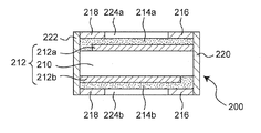
- the PTC device 200 includes a PTC element 212 and first and second insulating layers 214a and 214b disposed on both sides thereof.
- the PTC element 212 includes a PTC element 210 and a first layered electrode 212a and a second layered electrode 212b disposed on both sides thereof.
- the layered electrode 212 a is connected to the first side electrode 220, and the layered electrode 212 b is connected to the second side electrode 222.
- the first side electrode 220 and the second side electrode 222 are formed of a metal plating layer.
- the first side electrode 220 includes, in addition to the electrode portion in the thickness direction at one end of the PTC element 210, an electrode portion 216 and a second electrode portion 216 positioned on the one end portion of the first insulating layer 214a.
- An electrode portion 216 located on the one end portion of the insulating layer 214b is integrally formed.
- the second side electrode 222 includes an electrode portion 218 and a second electrode portion 218 positioned on the other end portion of the first insulating layer 214a in addition to the electrode portion in the thickness direction at the other end of the PTC element 210.
- An electrode portion 218 located on the other end portion of the insulating layer 214b is integrally formed.
- An intermediate region between the electrode portions 216 and 218 is covered with solder masks 224a and 224b (insulator).
- This direct electrical connection may be carried out by providing a through-hole directly connecting the electrode portion and the layered electrode in the insulating layer and providing a conductive element in the through-hole. More specifically, a conductive metal layer (eg, a plating layer) may be provided on the wall defining the through hole, and in another aspect, a conductive material such as a conductive paste is applied to the through hole. May be carried out by filling.
- a conductive metal layer eg, a plating layer
- the present invention provides: A layered PTC element defined by opposing first and second main surfaces, and a first layered electrode extending on the first main surface and a second layered electrode extending on the second main surface A first insulating layer located on the first main surface via the first layered electrode, and a second insulating layer located on the second main surface via the second layered electrode, A PTC device comprising a laminate in which a first insulating layer, a PTC element, and a second insulating layer are laminated in this order,
- the stacked body has a first end and a second end in a direction perpendicular to the stacking direction (that is, the up-down direction), and the first side electrode and the first end are provided on the first end and the second end, respectively.
- the first layered electrode of the PTC element extends away from the first side electrode and the second side electrode
- the second layered electrode of the PTC element is spaced from the first end, extends to the second end and is electrically connected to the second side electrode
- At least the first side electrode extends along the entire thickness direction of the stacked body at the first end, and further extends on the first end portion of the first insulating layer
- the first end portion has a through hole (also referred to as a via hole) that reaches the first layered electrode, and the through hole has a conductive element that electrically connects the first layered electrode and the first side electrode.
- a PTC device is provided.
- the present invention provides an electric apparatus comprising the PTC device of the present invention described above and below.
- an electric device includes a user interface such as a battery pack, USB, and HDMI, and the PTC device of the present invention functions as a circuit protection element, an overheat protection element, and the like.
- the layered electrode of the PTC element is electrically connected to the side electrode by the through-hole provided in the insulating layer and the conductive element located there, and the connecting portion in the layered electrode is the through-hole. It becomes a contact surface with the bottom face part of.
- the PTC device of the present invention in which the connection is achieved by surface contact, compared to the case where the connection portion is substantially linear and the layered electrode is directly connected to the side electrode, Increases area.
- the area of the connecting portion can be further increased by increasing the diameter of the through hole and / or increasing the number of through holes.
- the conductive element is isolated from the PTC element, so the mechanical stress generated from the volume expansion and contraction of the PTC element during operation of the PTC element due to overcurrent or overheating is alleviated. It is believed that more appropriate maintenance of these electrical connections is ensured.
- FIG. 1 schematically shows a perspective view of one embodiment of a PTC device of the present invention.
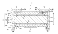
- FIG. 2 schematically shows a cross-sectional view of the PTC device shown in FIG. 1.
- a sectional view of a PTC device of another mode of the present invention is typically shown.
- a sectional view of a PTC device of another mode of the present invention is typically shown.
- a sectional view of a PTC device of another mode of the present invention is typically shown.
- a sectional view of a PTC device of another mode of the present invention is typically shown.
- a sectional view of a PTC device of another mode of the present invention is typically shown.
- 1 schematically shows a cross-sectional view of a prior art PTC device.
- FIG. 1 is a perspective view of a preferred embodiment of the PTC device of the present invention
- FIG. 2 is a cross-section generated when cut along a vertical section including a center line indicated by a one-dot chain line in FIG. This is shown schematically.
- a PTC device 10 shown in FIG. 1 includes a PTC element 12, a first insulating layer 14 located on the upper side, and a second insulating layer 16 located on the lower side.
- the PTC element 12 includes a layered PTC element 22 defined by opposing first and second main surfaces 18 and 20, and a first layered electrode 24 and a second main surface 20 extending on the first main surface 18. It has the 2nd layered electrode 26 extended by. Therefore, the PTC device 10 includes a stacked body 28 in which the first insulating layer 14, the PTC element 12, and the second insulating layer 16 are stacked in this order, and the first insulating layer 14 includes the first layered electrode 24.
- the second insulating layer 16 is located on the second main surface 20 via the second layered electrode 26.
- the stacked body 28 has a first end 30 and a second end 32 with respect to a direction perpendicular to the stacking direction (that is, the vertical direction indicated by the arrow A in FIG. 2).
- the first side electrode 34 and the second side electrode 36 are disposed on the second end portion 32, respectively.
- the first layered electrode 24 of the PTC element 12 is separated from the first side electrode 34 and the second side electrode 36, and the second layered electrode 26 of the PTC element 12 is Although it is separated from the first side electrode 34, it extends to the second end portion 32 and is electrically connected to the second side electrode 36 (more specifically, the thickness direction portion of the laminate described later). Connected.
- the first side electrode 34 extends along the entire thickness direction of the stacked body 28 at the first end 30, and further extends on the first end portion 38 of the first insulating layer 14. Includes a through hole 40 (also referred to as a via hole) that reaches the first layered electrode 24, and the via hole 40 includes a conductive element 42 that electrically connects the first layered electrode 24 and the first side electrode 34. .
- the conductive element 42 may be a metal plating layer formed on the inner wall that defines the via hole 40.
- the conductive element 42 may be a conductive composition filled in the via hole 40, such as a solder adhesive, a solder paste, a conductive adhesive, or the like.
- the first side electrode 34 not only extends along the thickness direction of the stacked body, but a portion 44 of the first side electrode 34 extends to the first end portion 38 of the first insulating layer 14.
- the other portion 46 extends along the first end portion 48 of the second insulating layer 16.
- the second side electrode 36 not only extends along the thickness direction of the stacked body, but also a portion 50 thereof extends along the second end portion 52 of the first insulating layer 14.
- the other portion 54 extends along the second end portion 56 of the second insulating layer 16.
- Each of the side electrodes is composed of the metal foil 58 thermocompression-bonded on the end portion of the insulating layer and the copper layer 60 plated thereon, and the portion 62 along the thickness direction of the laminate is laminated. It is composed of a copper layer plated on the body.
- such a side electrode is covered with the Ni / Sn layer 64 by plating, for example, so as not to be exposed as it is.
- the plating layer is formed only in the portion where the recess is formed at the end. Therefore, in the illustrated embodiment, each of the side electrodes is constituted by the thickness direction portion 62 (only the concave portion), the portion 44 and the portion 46 of the laminated body.
- the illustrated PTC device has one via hole 40, but the number of via holes is not particularly limited, and a plurality of, for example, two or more may be provided. Further, the position where the via hole is formed is not particularly limited, but it is preferably provided at a location near the side electrode from the viewpoint of increasing the rated current of the PTC element. For example, in FIG. 1, you may provide in one place on the near side of a dashed-dotted line and the other side, ie, two places.
- the illustrated PTC device 10 may be manufactured by any suitable method that can be configured as illustrated by sequentially forming the components that make up the PTC device 10.
- the elements constituting the PTC device of the present invention are all known, and those skilled in the art can form each element by selecting an appropriate material and an appropriate method.
- a PTC device assembly in which a number of PTC devices shown in FIG. 1 are connected in the vertical and horizontal directions (as indicated by broken lines in FIG. 1) is formed, cut along a plane including a straight line indicated by X1, and then indicated by X2.
- a plurality of individually divided PTC devices are manufactured by cutting along a plane including a straight line, then cutting along a plane including a straight line indicated by Y1, and finally cutting along a plane including a straight line indicated by Y2. Is convenient.
- a PTC device assembly can be formed as follows: First, metal foils constituting the layered electrodes 24 and 26 are stacked on the main surfaces on both sides of the extruded sheet of the PTC composition constituting the layered PTC element 22, and these are integrally thermocompression bonded to form a PTC element precursor sheet (" Prepare plaque (also called “plaque”). In order to form an assembly of the first layered electrode and the second layered electrode in the PTC assembly, the metal foils on both sides of the precursor sheet are respectively etched away in a predetermined manner so that predetermined portions of the layered PTC element 22 are removed. Expose. That is, as shown in FIG. 2, with respect to the first layered electrode 24, the first end 30 side and the second end 32 side of the layered PTC element 22 are exposed, and with respect to the second layered electrode 26, the layered PTC element is exposed. Only the first end 30 side of 22 is exposed.
- the prepreg sheets constituting the first insulating layer 14 and the second insulating layer 16 are laminated on each side of the precursor sheet to form a laminated body, on which the first insulating layer of the laminated body is formed. And a metal foil which finally constitutes a part of the first side electrode (parts 44 and 46) and a part of the second side electrode (parts 50 and 54) at the ends of the second insulating layer, respectively, And the prepreg sheet is melted and cured, and thermocompression bonded together.
- the through portion 45 having a circular cross section is formed by, for example, a mechanical drill so as to form a wall portion on which the first side electrode 34 and the second side electrode 36 extending along the thickness direction of the laminate are to be formed. (See FIG. 1). Further, for example, by melting the prepreg layer using laser CO 2 irradiation, a via hole 40 is formed at a predetermined location, and a desmear process (residue process) is performed. Thereafter, the entire precursor sheet is, for example, plated with copper to form a copper layer on the metal foil. As a result, the first side electrode portion 62 and the second side electrode portion 62 extending in the thickness direction of the laminate at both ends of the laminate are formed as copper layers.
- the copper layer is also formed on the outermost part of the precursor sheet (these will eventually constitute the portions 44, 46, 50 and 54) and also on the wall portion defining the via hole 40. Formed, which functions as the conductive element 42.
- the conductive element 42 may be in a state where the via hole is filled with copper depending on the size of the via hole.
- the first side electrode and a part of the second side electrode located on the first end portion and the second end portion of the first insulating layer and the second insulating layer of the PTC device are removed by etching to obtain a precursor sheet in which the insulating layer is exposed in a predetermined shape.
- the obtained precursor sheet is subjected to, for example, Ni / Sn plating to form a Ni / Sn film 64 on the surface of the exposed copper plating layer as can be understood from FIG.
- the first side electrode and the second side electrode thus obtained are obtained, and the PTC device assembly is completed.
- the device of the present invention can perform automatic mounting and reflow soldering, so in addition to high connection reliability by solder, It can also contribute to cost reduction of board mounting. Note that, since the exposed insulating layer has a large exposed area, the plating layer is not substantially formed.
- the individual PTC device assembly of the present invention is divided by dividing the completed PTC device assembly along the plane including the broken line X1, the plane including X2, the plane including Y1, and the plane including Y2 as shown in FIG. Get the device.
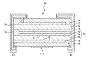
- FIG. 3 schematically shows a PTC device 70 according to another aspect of the present invention, as in FIG.
- FIG. 3 there are elements that are not denoted by reference numerals, but these elements are substantially the same as the corresponding elements in FIG.
- one other PTC element 72 and a third insulating layer 74 adjacent below the other PTC element 12 are arranged.
- the laminate 28 is constructed.
- the other PTC element 72 includes a PTC element 76 and a third layered electrode 78 and a fourth layered electrode 80 disposed on the third main surface 77 and the fourth main surface 79 facing each other. Have.
- the first insulating layer 14, the PTC element 12 and the second insulating layer 16, another PTC element 72 positioned on the second insulating layer, and the third insulating layer 74 adjacent thereto. are stacked in this order, and as a result, any PTC element is sandwiched between insulating layers.
- the first side electrode 34 is located on the left side of the figure
- the second side electrode 36 is located on the right side of the figure
- the fourth layered electrode 80 of another PTC element 72 is , Extending to the first end 30 of the stack and electrically connected to the first side electrode 34, while being spaced from the second end 32, the third layered electrode 78 is the first end of the stack Separated from the portion 30, the other end extends to the second end portion 32 and is electrically connected to the second side electrode 36.
- the two PTC elements 12 and 72 are electrically connected in parallel.
- the number of other PTC elements as described above is one in the embodiment shown in FIG. 3, but may be two or more (eg, three, four or more), in which case such another An insulating layer exists adjacent to the PTC element, and as a result, any PTC element is sandwiched between the insulating layers.
- at least one PTC element is disposed between the PTC element 12 and another PTC element 72, and any PTC element is sandwiched between insulating layers.
- one of the layered electrodes is electrically connected to the first side electrode and the other is electrically connected to the second side electrode, whereby these PTC elements are electrically connected in parallel.
- the rated current / rated voltage value of the PTC device becomes a multiple of the number of PTC elements to which the rated current / rated voltage value of each PTC element is connected.
- the mode shown in FIG. 3 is the same as the PTC element shown in FIG.
- FIG. 4 schematically shows a PTC device 90 according to another aspect of the present invention, as in FIG.
- the elements are substantially the same as the corresponding elements in FIG. 2.
- the layered PTC element 22 of the PTC element 12 has the first side electrode 34 by the insulating portion 92 at the first end 30 of the laminate 28. Is essentially different in that it is separated from
- seat which comprises the 1st insulating layer 14 and the 2nd insulating layer 16 on both sides of a precursor sheet
- FIG. 5 schematically shows a PTC device 100 according to another aspect of the present invention, as in FIG.
- the elements are substantially the same as the corresponding elements in FIG. 3.
- the layered PTC element 22 of the PTC element 12 has the first side electrode 34 by the insulating portion 92 at the first end 30 of the laminate 28. Is essentially different in that it is separated from The insulating portion 92 may be the same as that described above with reference to FIG.
- FIG. 6 schematically shows a PTC device 110 according to another aspect of the present invention, as in FIG.
- the second layered electrode 26 is separated from the second side electrode 36, and the second side electrode 36 is The second end portion 32 extends on the second end portion 56 of the second insulating layer 16 along the entire thickness direction of the stacked body, and the second end portion 56 reaches the second layered electrode 26.
- the second through hole 41 (also referred to as a via hole) is essentially different in that it has a conductive element 43 that electrically connects the second layered electrode 26 and the second side electrode 36.
- the second side electrode 36 is configured in substantially the same manner as the first side electrode 34.
- the electrode portion 44 on the first end portion 38 and the second end portion 52 of the first insulating layer 14 are provided.
- the length of the electrode portion 54 (or 55) on the second end portion 56 (or 57) is clearly longer than the length of the electrode portion 54 (or 57).
- These PTC devices are also marked with 112.
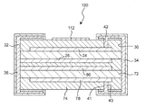
- FIG. 7 schematically shows a PTC device 120 according to another aspect of the present invention, as in FIG.
- the elements are substantially the same as the corresponding elements in FIG. 3.
- the insulating layer 74 is present outside the other PTC element 72 with the third layered electrode 78 interposed therebetween, and the third layered electrode 78 is formed in the via hole 41. This is essentially different in that it is connected to the first side electrode 34 via a conductive element 43 provided in FIG.
- the third layered electrode 78 is separated from the first side electrode 34 and the second side electrode 36 similarly to the first layered electrode 24, and the fourth layered electrode 80 inside another PTC element 72 is Similar to the two-layer electrode 26, it extends to the second end portion 32 and is electrically connected to the second side electrode 36 while being separated from the first side electrode 34.
- the first layered electrode 24 and the third layered electrode 78 are connected to the first side electrode 34 via conductive elements 42 and 43, respectively, while the second layered electrode 26 and the fourth layered electrode 80 are Two side electrodes 36 are connected.
- the third layered electrode 78 is connected to the first side electrode 34 by providing the through hole 41 and the conductive element 43 at the first end portion of the third insulating layer 74.
- the through hole 41 and the conductive element 43 may be provided at the second end portion of the third insulating layer 74.
- the third layered electrode 78 of the outermost PTC element is connected to the second side electrode 36.
- the fourth layered electrode 80 needs to be separated from the second side electrode 36 and connected to the first side electrode 34.
- the above-mentioned third layered electrode 78 is applied to another PTC element located on the outermost side, and the other PTC elements are remaining.
- one layered electrode is spaced from the second end, extends to the first end and is electrically connected to the first side electrode, and the other layered electrode is spaced from the first end. And extending to the second end and electrically connected to the second side electrode.
- PTC element 212a ... 1st layered electrode, 212b ... 2nd layered electrode, 214a ... 1st insulating layer, 214b ... second insulating layer, 216 ... electrode portion, 218 ... electrode portion, 220 ... first side electrode, 222 ... second side electrode, 224a, 224b ... solder mask.
Landscapes
- Engineering & Computer Science (AREA)
- Microelectronics & Electronic Packaging (AREA)
- Ceramic Engineering (AREA)
- Physics & Mathematics (AREA)
- Electromagnetism (AREA)
- Thermistors And Varistors (AREA)
- Details Of Resistors (AREA)
Abstract
Description
対向する第1主表面および第2主表面により規定される層状PTC要素、ならびに第1主表面上で延在する第1層状電極および第2主表面上で延在する第2層状電極を有して成るPTC素子、ならびに
第1層状電極を介して第1主表面上に位置する第1絶縁層、および第2層状電極を介して第2主表面上に位置する第2絶縁層
を有し、
第1絶縁層、PTC素子および第2絶縁層がこの順序で積層された積層体を有して成るPTCデバイスであって、
積層体は、積層方向(即ち、上下方向)に対して垂直な方向において第1端部および第2端部を有し、また、第1端部および第2端部には第1側方電極および第2側方電極がそれぞれ配置され、
PTC素子の第1層状電極は、第1側方電極および第2側方電極から離隔された状態で延在し、
PTC素子の第2層状電極は、第1端部から離隔され、第2端部まで延在して第2側方電極に電気的に接続され、
少なくとも第1側方電極は、第1端部にて積層体の厚さ方向全体に沿って、更に第1絶縁層の第1端部分上で延在し、
第1端部分は、第1層状電極に達する貫通孔(ビアホールとも呼ばれる)を有し、貫通孔は、第1層状電極と第1側方電極とを電気的に接続する導電性要素を有する
ことを特徴とするPTCデバイスを提供する。
最初に、層状PTC要素22を構成するPTC組成物の押出シートの両側の主表面に層状電極24および26を構成する金属箔を重ね、これらを一体に熱圧着してPTC素子前駆体シート(「プラーク」または「プラック」(plaque)とも呼ばれる)を準備する。PTC集合体における第1層状電極および第2層状電極の集合体を形成するように、前駆体シートの両側の金属箔をそれぞれ所定のようにエッチング除去して、層状PTC要素22の所定の箇所を露出させる。即ち、図2に示すように、第1層状電極24に関しては、層状PTC要素22の第1端部30側および第2端部32側を露出させ、第2層状電極26に関しては、層状PTC要素22の第1端部30側のみを露出させる。
16…第2絶縁層、18…第1主表面、20…第2主表面、
22…層状PTC要素、24…第1層状電極、26…第2層状電極、
28…積層体、30…第1端部、32…第2端部、34…第1側方電極、
36…第2側方電極、38…第1端部分、40…貫通孔、41…第2貫通孔、
42…導電性要素、43…導電性要素、44…電極部分、45…貫通部、
46、47…電極部分、48、49…第1端部分、50…電極部分、
52…第2端部分、54、55…電極部分、56…第2端部分、
58…金属箔、60…銅層、62…積層体の厚さ方向に沿う部分、
64…Ni/Sn層、70…PTCデバイス、72…PTC素子、
74…第3絶縁層、76…PTC要素、77…第3主表面、
78…第3層状電極、79…第4主表面、80…第4層状電極、
90…PTCデバイス、92…絶縁部、100…PTCデバイス、
110…PTCデバイス、112…マーキング、120…PTCデバイス、
200…PTCデバイス、210…PTC要素、212…PTC素子、
212a…第1層状電極、212b…第2層状電極、214a…第1絶縁層、
214b…第2絶縁層、216…電極部分、218…電極部分、
220…第1側方電極、222…第2側方電極、
224a、224b…はんだマスク。
Claims (7)
- 対向する第1主表面および第2主表面により規定される層状PTC要素、ならびに第1主表面上で延在する第1層状電極および第2主表面上で延在する第2層状電極を有して成るPTC素子、ならびに
第1層状電極を介して第1主表面上に位置する第1絶縁層、および第2層状電極を介して第2主表面上に位置する第2絶縁層
を有し、
第1絶縁層、PTC素子および第2絶縁層がこの順序で積層された積層体を有して成るPTCデバイスであって、
積層体は、積層方向(即ち、上下方向)に対して垂直な方向において第1端部および第2端部を有し、また、第1端部および第2端部には第1側方電極および第2側方電極がそれぞれ配置され、
PTC素子の第1層状電極は、第1側方電極および第2側方電極から離隔された状態で延在し、
PTC素子の第2層状電極は、第1端部から離隔され、第2端部まで延在して第2側方電極に電気的に接続され、
少なくとも第1側方電極は、第1端部にて積層体の厚さ方向全体に沿って、更に第1絶縁層の第1端部分上で延在し、
第1端部分は、第1層状電極に達する貫通孔を有し、貫通孔は、第1層状電極と第1側方電極とを電気的に接続する導電性要素を有する
ことを特徴とするPTCデバイス。 - 対向する第3主表面および第4主表面により規定される別の層状PTC要素、ならびに第3主表面上で延在する第3層状電極および第4主表面上で延在する第4層状電極をそれぞれが有して成る少なくとも1つの別のPTC素子を更に有して成り、
第1絶縁層、PTC素子および第2絶縁層、ならびに第2絶縁層上に位置する少なくとも1つの別のPTC素子および少なくとも1つの別のPTC素子のそれぞれに隣接する別の絶縁層がこの順序で積層され、その結果、いずれのPTC素子も絶縁層に挟まれた状態にある積層体を有して成り、
該少なくとも1つの別のPTC素子のそれぞれの第3層状電極は、第1端部から離隔され、第2端部まで延在して第2側方電極に電気的に接続され、
該少なくとも1つの別のPTC素子のそれぞれの第4層状電極は、第2端部から離隔され、第1端部まで延在して第1側方電極に電気的に接続されている
ことを特徴とする請求項1に記載のPTCデバイス。 - 該PTC素子の層状PTC要素は、積層体の第1端部にて絶縁部によって第1側方電極から離隔されていることを特徴とする請求項1または2に記載のPTCデバイス。
- PTC素子の第2層状電極は、第1側方電極および第2側方電極から離隔された状態で延在し、
第2側方電極は、第2端部にて積層体の厚さ方向全体に沿って、更に第2絶縁層の第2端部分上で延在し、
第2端部分は、第2層状電極に達する第2貫通孔を有し、貫通孔は、第2層状電極と第2側方電極とを電気的に接続する導電性要素を有する
ことを特徴とする請求項1に記載のPTCデバイス。 - 対向する第3主表面および第4主表面により規定される別の層状PTC要素、ならびに第3主表面上で延在する第3層状電極および第4主表面上で延在する第4層状電極をそれぞれが有して成る少なくとも1つの別のPTC素子を更に有して成り、
第1絶縁層、PTC素子および第2絶縁層、ならびに第2絶縁層上に位置する少なくとも1つの別のPTC素子および少なくとも1つの別のPTC素子のそれぞれに隣接する別の絶縁層がこの順序で積層され、その結果、いずれのPTC素子も絶縁層に挟まれた状態にある積層体を有して成り、
該少なくとも1つの別のPTC素子のうち、積層体の最外側に位置するPTC素子以外のそれぞれのPTC素子の第3層状電極は、第1端部から離隔され、第2端部まで延在して第2側方電極に電気的に接続され、
該少なくとも1つの別のPTC素子のうち、積層体の最外側に位置するPTC素子以外のそれぞれのPTC素子の第4層状電極は、第2端部から離隔され、第1端部まで延在して第1側方電極に電気的に接続され、
積層体の最外側に位置するPTC素子は、そのPTC要素の外側に第3層状電極を隔てて第3絶縁層を有し、第3層状電極は、第1側方電極および第2側方電極から離隔され、
積層体の最外側に位置するPTC素子の内側の第4層状電極は、第1側方電極から離隔された状態で、第2端部まで延在して第2側方電極に電気的に接続され、
第1側方電極は、第1端部にて積層体の厚さ方向全体に沿って、更に第1絶縁層および第3絶縁層の第1端部分上で延在し、
第3絶縁層の第1端部分は、積層体の最外側に位置するPTC素子の外側の第3層状電極に達する貫通孔を有し、貫通孔は、該第3層状電極と第1側方電極とを電気的に接続する導電性要素を有する
ことを特徴とする請求項1に記載のPTCデバイス。 - 対向する第3主表面および第4主表面により規定される別の層状PTC要素、ならびに第3主表面上で延在する第3層状電極および第4主表面上で延在する第4層状電極をそれぞれが有して成る少なくとも1つの別のPTC素子を更に有して成り、
第1絶縁層、PTC素子および第2絶縁層、ならびに第2絶縁層上に位置する少なくとも1つの別のPTC素子および少なくとも1つの別のPTC素子のそれぞれに隣接する別の絶縁層がこの順序で積層され、その結果、いずれのPTC素子も絶縁層に挟まれた状態にある積層体を有して成り、
該少なくとも1つの別のPTC素子のうち、積層体の最外側に位置するPTC素子以外のそれぞれのPTC素子の第3層状電極は、第1端部から離隔され、第2端部まで延在して第2側方電極に電気的に接続され、
該少なくとも1つの別のPTC素子のうち、積層体の最外側に位置するPTC素子以外のそれぞれのPTC素子の第4層状電極は、第2端部から離隔され、第1端部まで延在して第1側方電極に電気的に接続され、
積層体の最外側に位置するPTC素子は、そのPTC要素の外側に第3層状電極を隔てて第3絶縁層を有し、第3層状電極は、第1側方電極および第2側方電極から離隔され、
積層体の最外側に位置するPTC素子の内側の第4層状電極は、第2側方電極から離隔された状態で、第1端部まで延在して第1側方電極に電気的に接続され、
第2側方電極は、第2端部にて積層体の厚さ方向全体に沿って、更に第3絶縁層の第2端部分上で延在し、
第3絶縁層の第1端部分は、積層体の最外側に位置するPTC素子の外側の第3層状電極に達する貫通孔を有し、貫通孔は該第3層状電極と第1側方電極とを電気的に接続する導電性要素を有する
ことを特徴とする請求項1に記載のPTCデバイス。 - 該PTC素子および別のPTC素子の少なくとも1つの層状PTC要素は、積層体の第1端部または第2端部にて、絶縁部によって第1側方電極または第2側方電極から離隔されていることを特徴とする請求項5または6に記載のPTCデバイス。
Priority Applications (4)
| Application Number | Priority Date | Filing Date | Title |
|---|---|---|---|
| JP2013526894A JP6382514B2 (ja) | 2011-07-29 | 2012-07-27 | Ptcデバイス |
| US14/235,608 US9142949B2 (en) | 2011-07-29 | 2012-07-27 | PTC device |
| CN201280045782.XA CN103843079B (zh) | 2011-07-29 | 2012-07-27 | Ptc装置 |
| KR20147004683A KR20140062470A (ko) | 2011-07-29 | 2012-07-27 | Ptc 디바이스 |
Applications Claiming Priority (2)
| Application Number | Priority Date | Filing Date | Title |
|---|---|---|---|
| JP2011-167266 | 2011-07-29 | ||
| JP2011167266 | 2011-07-29 |
Publications (1)
| Publication Number | Publication Date |
|---|---|
| WO2013018719A1 true WO2013018719A1 (ja) | 2013-02-07 |
Family
ID=47629242
Family Applications (1)
| Application Number | Title | Priority Date | Filing Date |
|---|---|---|---|
| PCT/JP2012/069214 Ceased WO2013018719A1 (ja) | 2011-07-29 | 2012-07-27 | Ptcデバイス |
Country Status (6)
| Country | Link |
|---|---|
| US (1) | US9142949B2 (ja) |
| JP (1) | JP6382514B2 (ja) |
| KR (1) | KR20140062470A (ja) |
| CN (1) | CN103843079B (ja) |
| TW (1) | TWI552172B (ja) |
| WO (1) | WO2013018719A1 (ja) |
Families Citing this family (6)
| Publication number | Priority date | Publication date | Assignee | Title |
|---|---|---|---|---|
| WO2012173183A1 (ja) * | 2011-06-17 | 2012-12-20 | タイコエレクトロニクスジャパン合同会社 | Ptcデバイス |
| KR102397994B1 (ko) | 2015-03-10 | 2022-05-12 | 삼성에스디아이 주식회사 | 보호소자 및 이를 포함하는 이차 전지 |
| US9959958B1 (en) * | 2017-08-01 | 2018-05-01 | Fuzetec Technology Co., Ltd. | PTC circuit protection device and method of making the same |
| CN107741242B (zh) * | 2017-09-07 | 2019-09-10 | 感至源电子科技(上海)有限公司 | 屏蔽型传感器端子的制备方法 |
| US11404186B1 (en) * | 2021-04-23 | 2022-08-02 | Fuzetec Technology Co., Ltd. | PTC circuit protection device |
| TWI814547B (zh) * | 2022-08-24 | 2023-09-01 | 聚鼎科技股份有限公司 | 電路保護元件 |
Citations (4)
| Publication number | Priority date | Publication date | Assignee | Title |
|---|---|---|---|---|
| JP2001524747A (ja) * | 1997-11-26 | 2001-12-04 | リトルヒューズ, インコーポレイテッド | Ptcおよび可融性素子を含む表面実装可能電気デバイス |
| JP2003515245A (ja) * | 1999-09-14 | 2003-04-22 | タイコ・エレクトロニクス・コーポレイション | 電気デバイス及びそのようなデバイスを製造する方法 |
| JP2006510204A (ja) * | 2002-12-11 | 2006-03-23 | ブアンズ・インコーポレイテッド | 導電性高分子素子及びその製造方法 |
| JP2009533880A (ja) * | 2006-04-14 | 2009-09-17 | ブアンズ・インコーポレイテッド | 面実装が可能な導電性ポリマー電子デバイスとその製造方法 |
Family Cites Families (19)
| Publication number | Priority date | Publication date | Assignee | Title |
|---|---|---|---|---|
| US4980541A (en) * | 1988-09-20 | 1990-12-25 | Raychem Corporation | Conductive polymer composition |
| JPH02128414A (ja) * | 1988-11-07 | 1990-05-16 | Murata Mfg Co Ltd | 積層コンデンサ |
| US5378407A (en) * | 1992-06-05 | 1995-01-03 | Raychem Corporation | Conductive polymer composition |
| US5900800A (en) * | 1996-01-22 | 1999-05-04 | Littelfuse, Inc. | Surface mountable electrical device comprising a PTC element |
| TW415624U (en) | 1999-04-26 | 2000-12-11 | Polytronics Technology Corp | Surface mounted electric apparatus |
| TW507220B (en) * | 2001-03-13 | 2002-10-21 | Protectronics Technology Corp | Surface mountable polymeric circuit protection device and its manufacturing process |
| JP2003297604A (ja) * | 2002-03-29 | 2003-10-17 | Tdk Corp | チップ型過電流保護素子 |
| US20060055501A1 (en) | 2002-12-10 | 2006-03-16 | Bourns., Inc | Conductive polymer device and method of manufacturing same |
| TWI230453B (en) * | 2003-12-31 | 2005-04-01 | Polytronics Technology Corp | Over-current protection device and manufacturing method thereof |
| US7414857B2 (en) * | 2005-10-31 | 2008-08-19 | Avx Corporation | Multilayer ceramic capacitor with internal current cancellation and bottom terminals |
| US7697262B2 (en) * | 2005-10-31 | 2010-04-13 | Avx Corporation | Multilayer ceramic capacitor with internal current cancellation and bottom terminals |
| US8044763B2 (en) * | 2005-12-27 | 2011-10-25 | Polytronics Technology Corp. | Surface-mounted over-current protection device |
| TWI282696B (en) * | 2005-12-27 | 2007-06-11 | Polytronics Technology Corp | Surface-mounted over-current protection device |
| CN101740189A (zh) * | 2009-12-31 | 2010-06-16 | 上海长园维安电子线路保护股份有限公司 | 表面贴装型过电流保护元件 |
| TWI429157B (zh) * | 2011-01-17 | 2014-03-01 | Polytronics Technology Corp | 過電流保護裝置及其製備方法 |
| TWI433169B (zh) * | 2012-01-20 | 2014-04-01 | Polytronics Technology Corp | 表面黏著型熱敏電阻元件 |
| US8502638B1 (en) * | 2012-02-03 | 2013-08-06 | Polytronics Technology Corp. | Thermistor |
| TWI456596B (zh) * | 2012-07-31 | 2014-10-11 | Polytronics Technology Corp | 過電流保護元件及其製作方法 |
| TWI441201B (zh) * | 2012-09-28 | 2014-06-11 | Polytronics Technology Corp | 表面黏著型過電流保護元件 |
-
2012
- 2012-07-27 TW TW101127140A patent/TWI552172B/zh active
- 2012-07-27 US US14/235,608 patent/US9142949B2/en active Active
- 2012-07-27 KR KR20147004683A patent/KR20140062470A/ko not_active Ceased
- 2012-07-27 WO PCT/JP2012/069214 patent/WO2013018719A1/ja not_active Ceased
- 2012-07-27 CN CN201280045782.XA patent/CN103843079B/zh active Active
- 2012-07-27 JP JP2013526894A patent/JP6382514B2/ja active Active
Patent Citations (4)
| Publication number | Priority date | Publication date | Assignee | Title |
|---|---|---|---|---|
| JP2001524747A (ja) * | 1997-11-26 | 2001-12-04 | リトルヒューズ, インコーポレイテッド | Ptcおよび可融性素子を含む表面実装可能電気デバイス |
| JP2003515245A (ja) * | 1999-09-14 | 2003-04-22 | タイコ・エレクトロニクス・コーポレイション | 電気デバイス及びそのようなデバイスを製造する方法 |
| JP2006510204A (ja) * | 2002-12-11 | 2006-03-23 | ブアンズ・インコーポレイテッド | 導電性高分子素子及びその製造方法 |
| JP2009533880A (ja) * | 2006-04-14 | 2009-09-17 | ブアンズ・インコーポレイテッド | 面実装が可能な導電性ポリマー電子デバイスとその製造方法 |
Also Published As
| Publication number | Publication date |
|---|---|
| TWI552172B (zh) | 2016-10-01 |
| JPWO2013018719A1 (ja) | 2015-03-05 |
| JP6382514B2 (ja) | 2018-08-29 |
| CN103843079A (zh) | 2014-06-04 |
| TW201314711A (zh) | 2013-04-01 |
| US9142949B2 (en) | 2015-09-22 |
| CN103843079B (zh) | 2017-03-08 |
| US20150029630A1 (en) | 2015-01-29 |
| KR20140062470A (ko) | 2014-05-23 |
Similar Documents
| Publication | Publication Date | Title |
|---|---|---|
| TWI670742B (zh) | 電流熔絲 | |
| JP6382514B2 (ja) | Ptcデバイス | |
| JP6483987B2 (ja) | ヒューズエレメント、ヒューズ素子、及び発熱体内蔵ヒューズ素子 | |
| CN108701566B (zh) | 保护元件 | |
| WO2007119358A1 (ja) | 面実装型電流ヒューズ | |
| JP2006324555A (ja) | 積層型コンデンサ及びその製造方法 | |
| JP6124793B2 (ja) | Ptcデバイス | |
| TWI469158B (zh) | 過電流保護元件 | |
| JP4609042B2 (ja) | 固体電解コンデンサ及び固体電解コンデンサの製造方法 | |
| JP6152342B2 (ja) | Ptcデバイス | |
| TWI493576B (zh) | 過電流保護元件及其保護電路板 | |
| JP2006310277A (ja) | チップ型ヒューズ | |
| JP2003243257A (ja) | 固体電解コンデンサ | |
| JP5365420B2 (ja) | 積層型電子部品 | |
| TWI539472B (zh) | 過電流保護元件 | |
| JP4461641B2 (ja) | 積層型チップサーミスタ及びその製造方法 | |
| JP2006093337A (ja) | 固体電解コンデンサ | |
| JP5850499B2 (ja) | 固体電解コンデンサ | |
| JP2022063830A (ja) | 保護素子及びその製造方法 | |
| JP2020098940A (ja) | 積層コイル部品 | |
| JP2002260903A (ja) | 積層型電子部品の製造方法 |
Legal Events
| Date | Code | Title | Description |
|---|---|---|---|
| 121 | Ep: the epo has been informed by wipo that ep was designated in this application |
Ref document number: 12820244 Country of ref document: EP Kind code of ref document: A1 |
|
| ENP | Entry into the national phase |
Ref document number: 2013526894 Country of ref document: JP Kind code of ref document: A |
|
| NENP | Non-entry into the national phase |
Ref country code: DE |
|
| ENP | Entry into the national phase |
Ref document number: 20147004683 Country of ref document: KR Kind code of ref document: A |
|
| 122 | Ep: pct application non-entry in european phase |
Ref document number: 12820244 Country of ref document: EP Kind code of ref document: A1 |
|
| WWE | Wipo information: entry into national phase |
Ref document number: 14235608 Country of ref document: US |