WO2013018447A1 - 半導体素子の製造方法 - Google Patents
半導体素子の製造方法 Download PDFInfo
- Publication number
- WO2013018447A1 WO2013018447A1 PCT/JP2012/065615 JP2012065615W WO2013018447A1 WO 2013018447 A1 WO2013018447 A1 WO 2013018447A1 JP 2012065615 W JP2012065615 W JP 2012065615W WO 2013018447 A1 WO2013018447 A1 WO 2013018447A1
- Authority
- WO
- WIPO (PCT)
- Prior art keywords
- insulating film
- film
- manufacturing
- heat treatment
- thickness
- Prior art date
- Legal status (The legal status is an assumption and is not a legal conclusion. Google has not performed a legal analysis and makes no representation as to the accuracy of the status listed.)
- Ceased
Links
Images
























Classifications
-
- H—ELECTRICITY
- H10—SEMICONDUCTOR DEVICES; ELECTRIC SOLID-STATE DEVICES NOT OTHERWISE PROVIDED FOR
- H10D—INORGANIC ELECTRIC SEMICONDUCTOR DEVICES
- H10D99/00—Subject matter not provided for in other groups of this subclass
-
- H—ELECTRICITY
- H10—SEMICONDUCTOR DEVICES; ELECTRIC SOLID-STATE DEVICES NOT OTHERWISE PROVIDED FOR
- H10D—INORGANIC ELECTRIC SEMICONDUCTOR DEVICES
- H10D30/00—Field-effect transistors [FET]
- H10D30/60—Insulated-gate field-effect transistors [IGFET]
- H10D30/67—Thin-film transistors [TFT]
- H10D30/6704—Thin-film transistors [TFT] having supplementary regions or layers in the thin films or in the insulated bulk substrates for controlling properties of the device
-
- H—ELECTRICITY
- H10—SEMICONDUCTOR DEVICES; ELECTRIC SOLID-STATE DEVICES NOT OTHERWISE PROVIDED FOR
- H10D—INORGANIC ELECTRIC SEMICONDUCTOR DEVICES
- H10D30/00—Field-effect transistors [FET]
- H10D30/60—Insulated-gate field-effect transistors [IGFET]
- H10D30/67—Thin-film transistors [TFT]
- H10D30/6729—Thin-film transistors [TFT] characterised by the electrodes
- H10D30/673—Thin-film transistors [TFT] characterised by the electrodes characterised by the shapes, relative sizes or dispositions of the gate electrodes
-
- H—ELECTRICITY
- H10—SEMICONDUCTOR DEVICES; ELECTRIC SOLID-STATE DEVICES NOT OTHERWISE PROVIDED FOR
- H10D—INORGANIC ELECTRIC SEMICONDUCTOR DEVICES
- H10D30/00—Field-effect transistors [FET]
- H10D30/60—Insulated-gate field-effect transistors [IGFET]
- H10D30/67—Thin-film transistors [TFT]
- H10D30/674—Thin-film transistors [TFT] characterised by the active materials
- H10D30/6755—Oxide semiconductors, e.g. zinc oxide, copper aluminium oxide or cadmium stannate
-
- H—ELECTRICITY
- H10—SEMICONDUCTOR DEVICES; ELECTRIC SOLID-STATE DEVICES NOT OTHERWISE PROVIDED FOR
- H10D—INORGANIC ELECTRIC SEMICONDUCTOR DEVICES
- H10D86/00—Integrated devices formed in or on insulating or conducting substrates, e.g. formed in silicon-on-insulator [SOI] substrates or on stainless steel or glass substrates
- H10D86/40—Integrated devices formed in or on insulating or conducting substrates, e.g. formed in silicon-on-insulator [SOI] substrates or on stainless steel or glass substrates characterised by multiple TFTs
- H10D86/421—Integrated devices formed in or on insulating or conducting substrates, e.g. formed in silicon-on-insulator [SOI] substrates or on stainless steel or glass substrates characterised by multiple TFTs having a particular composition, shape or crystalline structure of the active layer
- H10D86/423—Integrated devices formed in or on insulating or conducting substrates, e.g. formed in silicon-on-insulator [SOI] substrates or on stainless steel or glass substrates characterised by multiple TFTs having a particular composition, shape or crystalline structure of the active layer comprising semiconductor materials not belonging to the Group IV, e.g. InGaZnO
-
- H—ELECTRICITY
- H10—SEMICONDUCTOR DEVICES; ELECTRIC SOLID-STATE DEVICES NOT OTHERWISE PROVIDED FOR
- H10D—INORGANIC ELECTRIC SEMICONDUCTOR DEVICES
- H10D86/00—Integrated devices formed in or on insulating or conducting substrates, e.g. formed in silicon-on-insulator [SOI] substrates or on stainless steel or glass substrates
- H10D86/40—Integrated devices formed in or on insulating or conducting substrates, e.g. formed in silicon-on-insulator [SOI] substrates or on stainless steel or glass substrates characterised by multiple TFTs
- H10D86/60—Integrated devices formed in or on insulating or conducting substrates, e.g. formed in silicon-on-insulator [SOI] substrates or on stainless steel or glass substrates characterised by multiple TFTs wherein the TFTs are in active matrices
-
- H—ELECTRICITY
- H10—SEMICONDUCTOR DEVICES; ELECTRIC SOLID-STATE DEVICES NOT OTHERWISE PROVIDED FOR
- H10F—INORGANIC SEMICONDUCTOR DEVICES SENSITIVE TO INFRARED RADIATION, LIGHT, ELECTROMAGNETIC RADIATION OF SHORTER WAVELENGTH OR CORPUSCULAR RADIATION
- H10F39/00—Integrated devices, or assemblies of multiple devices, comprising at least one element covered by group H10F30/00, e.g. radiation detectors comprising photodiode arrays
- H10F39/011—Manufacture or treatment of image sensors covered by group H10F39/12
- H10F39/026—Wafer-level processing
-
- H—ELECTRICITY
- H10—SEMICONDUCTOR DEVICES; ELECTRIC SOLID-STATE DEVICES NOT OTHERWISE PROVIDED FOR
- H10F—INORGANIC SEMICONDUCTOR DEVICES SENSITIVE TO INFRARED RADIATION, LIGHT, ELECTROMAGNETIC RADIATION OF SHORTER WAVELENGTH OR CORPUSCULAR RADIATION
- H10F39/00—Integrated devices, or assemblies of multiple devices, comprising at least one element covered by group H10F30/00, e.g. radiation detectors comprising photodiode arrays
- H10F39/10—Integrated devices
- H10F39/12—Image sensors
- H10F39/18—Complementary metal-oxide-semiconductor [CMOS] image sensors; Photodiode array image sensors
- H10F39/189—X-ray, gamma-ray or corpuscular radiation imagers
- H10F39/1892—Direct radiation image sensors
-
- H—ELECTRICITY
- H10—SEMICONDUCTOR DEVICES; ELECTRIC SOLID-STATE DEVICES NOT OTHERWISE PROVIDED FOR
- H10F—INORGANIC SEMICONDUCTOR DEVICES SENSITIVE TO INFRARED RADIATION, LIGHT, ELECTROMAGNETIC RADIATION OF SHORTER WAVELENGTH OR CORPUSCULAR RADIATION
- H10F39/00—Integrated devices, or assemblies of multiple devices, comprising at least one element covered by group H10F30/00, e.g. radiation detectors comprising photodiode arrays
- H10F39/80—Constructional details of image sensors
- H10F39/803—Pixels having integrated switching, control, storage or amplification elements
- H10F39/8037—Pixels having integrated switching, control, storage or amplification elements the integrated elements comprising a transistor
- H10F39/80373—Pixels having integrated switching, control, storage or amplification elements the integrated elements comprising a transistor characterised by the gate of the transistor
-
- H—ELECTRICITY
- H10—SEMICONDUCTOR DEVICES; ELECTRIC SOLID-STATE DEVICES NOT OTHERWISE PROVIDED FOR
- H10P—GENERIC PROCESSES OR APPARATUS FOR THE MANUFACTURE OR TREATMENT OF DEVICES COVERED BY CLASS H10
- H10P14/00—Formation of materials, e.g. in the shape of layers or pillars
- H10P14/20—Formation of materials, e.g. in the shape of layers or pillars of semiconductor materials
- H10P14/34—Deposited materials, e.g. layers
- H10P14/3402—Deposited materials, e.g. layers characterised by the chemical composition
- H10P14/3434—Deposited materials, e.g. layers characterised by the chemical composition being oxide semiconductor materials
-
- H—ELECTRICITY
- H10—SEMICONDUCTOR DEVICES; ELECTRIC SOLID-STATE DEVICES NOT OTHERWISE PROVIDED FOR
- H10F—INORGANIC SEMICONDUCTOR DEVICES SENSITIVE TO INFRARED RADIATION, LIGHT, ELECTROMAGNETIC RADIATION OF SHORTER WAVELENGTH OR CORPUSCULAR RADIATION
- H10F39/00—Integrated devices, or assemblies of multiple devices, comprising at least one element covered by group H10F30/00, e.g. radiation detectors comprising photodiode arrays
- H10F39/10—Integrated devices
- H10F39/12—Image sensors
- H10F39/15—Charge-coupled device [CCD] image sensors
-
- H—ELECTRICITY
- H10—SEMICONDUCTOR DEVICES; ELECTRIC SOLID-STATE DEVICES NOT OTHERWISE PROVIDED FOR
- H10K—ORGANIC ELECTRIC SOLID-STATE DEVICES
- H10K59/00—Integrated devices, or assemblies of multiple devices, comprising at least one organic light-emitting element covered by group H10K50/00
- H10K59/10—OLED displays
- H10K59/12—Active-matrix OLED [AMOLED] displays
- H10K59/121—Active-matrix OLED [AMOLED] displays characterised by the geometry or disposition of pixel elements
- H10K59/1213—Active-matrix OLED [AMOLED] displays characterised by the geometry or disposition of pixel elements the pixel elements being TFTs
Definitions
- the present invention relates to a method for manufacturing a semiconductor element and a method for manufacturing a field effect transistor.
- field effect transistors are used in unit elements of semiconductor integrated circuits for semiconductor memories, high frequency signal amplifying elements, liquid crystal driving elements, and the like, and particularly thin-film transistors are used in a wide range of fields as thin film transistors (TFTs).
- TFTs thin film transistors
- a silicon semiconductor or a compound thereof As a semiconductor channel layer (active layer) for forming a field effect transistor, a silicon semiconductor or a compound thereof has been conventionally used in many cases. For high-frequency amplifying elements and integrated circuits that require high-speed operation, Although low-speed operation is sufficient, amorphous silicon is used for liquid crystal drive devices that are required to support large areas such as display applications, but amorphous silicon performance has been improved for larger size and higher definition. There is a demand for TFT characteristics that surpass it. Recently, flexible displays that are lightweight and bendable have attracted attention. For flexible devices, a highly flexible resin substrate is mainly used, and a lower temperature process is required than a liquid crystal display process (400 ° C.).
- the In-Ga-Zn-O system (hereinafter referred to as IGZO) has better electrical characteristics than amorphous silicon, and as an oxide semiconductor that can be manufactured by a liquid crystal process or a low temperature process, Tokyo Institute of Technology Hosono et al. Reported by. IGZO is regarded as a promising semiconductor element material for next-generation displays, and universities / manufacturers around the world are actively conducting research and development toward practical application.
- the performance required for semiconductor elements, particularly TFTs includes mobility, S value, Vth, etc., but a major issue for practical use is ⁇ Vth (threshold voltage shift: unit (V)) during TFT operation. . This is because oxides such as IGZO have low resistance to moisture, oxygen, contamination, etc., and if the active layer mainly composed of oxides such as IGZO is exposed to the atmosphere, the oxide will deteriorate over time. It is caused by that.
- ⁇ Vth is suppressed by forming a protective layer on the exposed surface of the active layer mainly composed of IGZO to protect the active layer from moisture and the like. That is, it can be said that a protective layer is essential in order to stably use an oxide such as IGZO as an active layer. Note that even in the case of a top-gate TFT, a gate insulating layer that also serves as a protective layer for the active layer is essential over the active layer.
- Non-patent Document 1 “Monthly display 2011.11 month issue Vol.17 NO1” Table 2 of “Recent trends and prospects of oxide TFT” ")
- stabilization of device characteristics such as ⁇ Vth at the time of light irradiation is a big issue.
- Patent Document 1 Japanese Patent Application Laid-Open No. 2010-183027
- a protective layer having a thickness of 200 nm is formed on the partially exposed surface of the active layer made of the IGZO film by using a sputtering method.
- a method of manufacturing a bottom gate TFT is disclosed in which a source / drain electrode having an opening is formed on another partially exposed surface, and then an interlayer insulating film having a thickness of 300 nm is formed.
- oxygen annealing is performed under the condition of 300 ° C. in an atmosphere having a nitrogen concentration of 60% and an oxygen concentration of 40%. It is also possible to recover the TFT characteristics by supplying oxygen from the opening and the exposed portion of the active layer to the deficient portion where oxygen in the active layer is insufficient or from which oxygen has been released. ing.
- Patent Document 2 Japanese Patent Application Laid-Open No. 2011-49550 discloses that in a method for manufacturing a bottom gate type TFT, a thickness of at least 1 nm or more is obtained by using a sputtering method on a partially exposed surface of an active layer made of an IGZO film. After forming the oxide insulating film, heat treatment is performed in an oxidizing atmosphere with a part of the active layer exposed before forming a protective insulating layer disposed on the oxide insulating film. Discloses that at least a part of the active layer is in an oxygen-excess state.
- Patent Document 3 in the manufacturing method of the bottom gate type TFT, the entire exposed surface of the active layer made of the IGZO film is protected to 100 to 700 nm using the CVD method. After forming the layer, before forming an interlayer insulating film disposed on the protective layer, heat treatment is performed at 220 ° C. or higher, so that the active layer is supplemented with oxygen through the protective layer. It is disclosed to control the oxygen content of.
- the protective layer and the gate insulating layer that also functions as the protective layer are essential on the exposed surface of the active layer, but the exposed surface of the active layer is damaged by the film formation thereof.
- a surface defect that affects ⁇ Vth during light irradiation may occur.
- surface defects may occur due to etching damage or physical damage.
- the exposed surface of the active layer is particularly damaged by the plasma, resulting in an increase in surface defects.
- Patent Document 3 discloses that this heat treatment supplements the active layer with oxygen through the protective layer and controls the oxygen content in the active layer, but plasma damage is caused by the formation of the protective layer. Since the surface of the received active layer is covered with a protective layer having a thickness of 100 to 700 nm, oxygen does not reach even after the heat treatment depending on the relationship between the heat treatment temperature and the film thickness of the protective layer. The surface defects of the active layer that has been damaged by plasma cannot be compensated.
- oxygen in the protective layer protects the active layer and not oxygen in the atmosphere. It is considered that oxygen is supplied to the active layer by reaching the interface with the layer.
- oxygen may be supplied through other than the protective layer. Then, only oxygen supply in the protective layer or oxygen supply through other than the protective layer cannot sufficiently compensate for surface defects on the surface of the active layer that has been damaged by plasma, and ⁇ Vth at the time of light irradiation does not improve. Conceivable.
- the present invention has been made in view of the above circumstances, and an object of the present invention is to provide a method for manufacturing a semiconductor element and a method for manufacturing a field effect transistor that stabilize element characteristics during light irradiation.
- ⁇ 1> a first step of forming a semiconductor film mainly composed of an oxide semiconductor; a second step of forming a first insulating film on the surface of the semiconductor film after the first step; A third step of heat-treating in an oxidizing atmosphere after two steps, and a fourth step of forming a second insulating film on the surface of the first insulating film after the third step,
- the thickness of the first insulating film is Z (nm)
- the heat treatment temperature in the third step is T (° C.)
- a method for manufacturing a semiconductor element wherein the thickness of the first insulating film and the heat treatment temperature are adjusted so as to satisfy the relational expression 1.
- the thickness of the first insulating film and the heat treatment temperature are adjusted so as to satisfy a relational expression of Z ⁇ L ⁇ 1.0.
- the thickness of the first insulating film and the heat treatment temperature are adjusted so as to satisfy a relational expression of Z ⁇ L ⁇ 2.0.
- the thickness of the first insulating film and the heat treatment temperature are adjusted so as to satisfy the relational expression L ⁇ 5.0 ⁇ Z. ⁇ 1> to ⁇ 3>
- the thickness of the first insulating film and the heat treatment temperature are adjusted so as to satisfy the relational expression of L ⁇ 2.0 ⁇ Z. ⁇ 1> or The manufacturing method of the semiconductor element as described in ⁇ 2>.
- ⁇ 6> The method for manufacturing a semiconductor element according to any one of ⁇ 1> to ⁇ 5>, wherein the thickness Z of the first insulating film is adjusted to 2 nm or more in the second step.
- ⁇ 7> Forming the first insulating film and the second insulating film using a film forming method that generates plasma during the second step and the fourth step, ⁇ 1> to ⁇ 6 > The manufacturing method of the semiconductor element as described in any one of>.
- ⁇ 8> The method for manufacturing a semiconductor element according to ⁇ 7>, wherein, in the second step, the film formation rate is decreased and the plasma potential is decreased or the film formation pressure is increased as compared with the film formation in the fourth step.
- ⁇ 9> The method for manufacturing a semiconductor element according to ⁇ 7> or ⁇ 8>, wherein, in the second step, the first insulating film is formed at a deposition rate of 20 nm / min or less.
- the first insulating film is formed in a film formation time shorter than the film formation time in which the second insulating film is formed in the fourth step.
- ⁇ 7> to ⁇ The manufacturing method of the semiconductor element as described in any one of 9>.
- ⁇ 11> The method for manufacturing a semiconductor element according to any one of ⁇ 1> to ⁇ 10>, wherein in the first step, the semiconductor film is formed to have a thickness of 5 nm or more.
- ⁇ 12> The method according to any one of ⁇ 1> to ⁇ 11>, further including a fifth step of performing a heat treatment at a temperature lower than the heat treatment temperature in the third step in an oxidizing atmosphere after the fourth step.
- ⁇ 13> The method for manufacturing a semiconductor element according to ⁇ 12>, wherein the heat treatment temperature in the fifth step is 100 ° C. or higher.
- ⁇ 14> The method for manufacturing a semiconductor element according to ⁇ 13>, wherein the heat treatment temperature in the fifth step is 300 ° C. or higher.
- ⁇ 15> Manufacturing the semiconductor element according to any one of ⁇ 1> to ⁇ 14>, wherein, in the fourth step, the second insulating film having a thickness larger than that of the first insulating film is formed.
- Method. ⁇ 16> The method for manufacturing a semiconductor element according to any one of ⁇ 1> to ⁇ 15>, wherein the oxide semiconductor is an amorphous oxide containing at least one of In, Ga, and Zn. .
- ⁇ 17> The method for manufacturing a semiconductor element according to any one of ⁇ 1> to ⁇ 16>, wherein the heat treatment temperature in the third step is less than 600 ° C.
- ⁇ 18> The method for manufacturing a semiconductor element according to any one of ⁇ 1> to ⁇ 17>, wherein in the second step, a first insulating film is formed over the entire surface of the semiconductor film.
- the constituent material of the second insulating film includes a metal
- the first insulating film includes at least a part of the constituent material of the second insulating film and the constituent material of the semiconductor film.
- the method for manufacturing a semiconductor device according to any one of ⁇ 1> to ⁇ 18> including both of a part of metals.
- the electrode forming step and the non-electrode forming step are performed in the order in which the gate electrode becomes a bottom gate type, and the first insulating film and the second insulating film are formed as protective layers for the semiconductor film.
- ⁇ 22> The method for producing a field effect transistor according to ⁇ 21>, wherein the total thickness of the first insulating film and the second insulating film is 30 nm or more.
- the source electrode and the drain electrode are formed between the first step and the second step so that the source electrode and the drain electrode are a top contact type in the electrode forming step, and
- the formation of the source electrode and the drain electrode is performed before the first step so that the source electrode and the drain electrode are of bottom contact type.
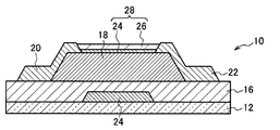
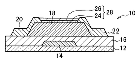
- FIG. 1A is a schematic diagram showing an example of a top contact type TFT having a bottom gate structure, which is a TFT according to an embodiment of the present invention.
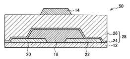
- FIG. 1B is a schematic diagram illustrating an example of a bottom contact type TFT having a bottom gate structure, which is a TFT according to an embodiment of the present invention.
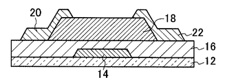
- FIG. 1C is a schematic diagram showing an example of a top contact type TFT having a top gate structure, which is a TFT according to an embodiment of the present invention.
- FIG. 1D is a schematic diagram showing an example of a bottom contact type TFT with a top gate structure, which is a TFT according to an embodiment of the present invention.
- FIG. 1A is a schematic diagram showing an example of a top contact type TFT having a bottom gate structure, which is a TFT according to an embodiment of the present invention.
- FIG. 1B is a schematic diagram illustrating an example of a bottom contact type TFT having a bottom gate structure, which is a T
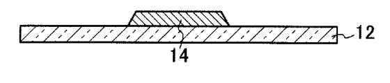
- FIG. 2A is a process diagram of a method for manufacturing a top-gate TFT having a bottom gate structure.
- FIG. 2B is a process diagram of the TFT manufacturing method subsequent to FIG. 2A.
- FIG. 2C is a process diagram of the manufacturing method of the TFT subsequent to FIG. 2B.
- FIG. 2D is a process diagram of the manufacturing method of the TFT subsequent to FIG. 2C.
- FIG. 2E is a process diagram of the manufacturing method of the TFT subsequent to FIG. 2D.
- FIG. 2F is a process diagram of the TFT manufacturing method subsequent to FIG. 2E.
- FIG. 2G is a process diagram of the manufacturing method of the TFT subsequent to FIG. 2F.
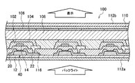
- FIG. 3 is a schematic cross-sectional view of a part of the liquid crystal display device according to the embodiment of the electro-optical device of the invention.
- FIG. 4 is a schematic configuration diagram of electrical wiring of the liquid crystal display device shown in FIG.
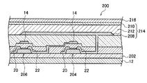
- FIG. 5 is a schematic cross-sectional view of a part of an active matrix type organic EL display device according to an embodiment of the electro-optical device of the invention.
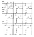
- FIG. 6 is a schematic configuration diagram of electrical wiring of the organic EL display device shown in FIG.
- FIG. 7 is a schematic cross-sectional view of a part of an X-ray sensor that is an embodiment of the sensor of the present invention.
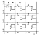
- FIG. 8 is a schematic configuration diagram of electric wiring of the X-ray sensor shown in FIG. FIG.
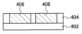
- FIG. 9A is a process diagram of the manufacturing method of the photodiode according to the embodiment of the present invention.
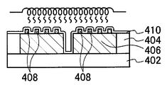
- FIG. 9B is a process diagram of the manufacturing method of the photodiode, following FIG. 9A.
- FIG. 9C is a process diagram of the manufacturing method of the photodiode, following FIG. 9B.
- FIG. 9D is a process diagram of the manufacturing method of the photodiode, following FIG. 9C.
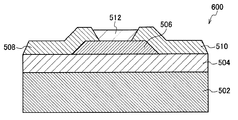
- FIG. 9E is a process diagram of the manufacturing method of the photodiode, following FIG. 9D.
- FIG. 10 is a cross-sectional view of a TFT obtained by preparing the sample of Experimental Example 1-1.
- FIG. 11 is a cross-sectional view of a TFT obtained by preparing the sample of Experimental Example 1-2.
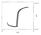
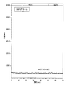
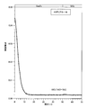
- FIG. 12 is a diagram showing a stress flow when measuring the Vg-Id characteristic.
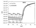
- FIG. 13 is a diagram illustrating a measurement result of the Vg-Id characteristic of the TFT according to Experimental Example 1-1.
- FIG. 14 is a diagram illustrating a measurement result of the Vg-Id characteristic of the TFT according to Experimental Example 1-2.
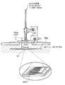
- FIG. 15 is a diagram showing a configuration for evaluating the light irradiation characteristics.
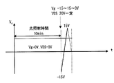
- FIG. 16 is a diagram showing a flow of light irradiation characteristic evaluation.
- FIG. 17 is a diagram illustrating a calculation result of ⁇ Vth at the time of light irradiation on the sample of Experimental Example 1-1.
- FIG. 18 is a diagram showing a calculation result of ⁇ Vth at the time of light irradiation on a sample in which a protective layer was formed on the exposed surface of the active layer of the sample of Experimental Example 1-1 by the same method as in Experimental Example 1-2. is there.
- FIG. 19 is a cross-sectional view of a TFT obtained by preparing the sample of Experimental Example 3-2.
- FIG. 20 is a diagram showing a measurement result of Vg-Id characteristics for the TFT according to Experimental example 3-1.
- FIG. 21 is a diagram showing a measurement result of Vg-Id characteristics for the TFT according to Experimental Example 3-2.
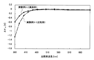
- FIG. 22 is a diagram illustrating a calculation result of ⁇ Vth at the time of light irradiation with respect to the TFT according to Experimental Example 3-1 and the TFT according to Experimental Example 3-2.
- FIG. 23 is a diagram showing a system configuration during heat treatment.
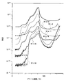
- FIG. 24 is a diagram showing the SIMS analysis results for the sample of Experimental Example 4-1.
- FIG. 25 is a diagram showing SIMS analysis results for the sample of Experimental Example 4-2.
- FIG. 26 is a diagram showing the SIMS analysis results for the sample of Experimental Example 4-3.
- FIG. 27 is a diagram showing SIMS analysis results for the sample of Experimental Example 4-4.
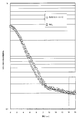
- FIG. 28 is a graph plotting the relationship between the obtained oxygen diffusion distance L and the heat treatment temperature.
- FIG. 29 is a diagram showing SIMS analysis results for the samples of Experimental Example 4-5.
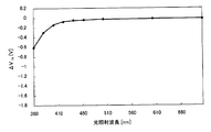
- FIG. 30 is a diagram showing the relationship between the light irradiation wavelength and ⁇ Vth for the samples according to Experimental Examples 5-1 to 5-6.
- FIG. 31 is a diagram showing the relationship between the thickness Z of the first insulating film and ⁇ Vth at the time of light irradiation for the samples according to Experimental Examples 5-1 to 5-6.
- FIG. 32 is a diagram showing the relationship between the thickness Z of the first insulating film and the mobility during light irradiation for the samples according to Experimental Examples 5-1 to 5-6.
- FIG. 33 is a diagram showing the results of temperature programmed desorption analysis in Experimental Example 6.
- FIG. 34 is a diagram showing In depth and secondary ion intensity by SIMS analysis.
- FIG. 35 is a diagram showing Zn depth and secondary ion intensity by SIMS analysis.
- FIG. 10 is a diagram showing SIMS analysis results for samples obtained by heat-treating three IGZO films of: 1.5: 1 under the same conditions as in Experimental Example 4-3 (however, the heat treatment temperature is 450 ° C.).
- analysis and, SiO 2 film experimental example 4-3 under the same conditions is a diagram showing SIMS analysis results of a sample heat-treated at.
- a method for manufacturing a semiconductor device includes a first step of forming a semiconductor film mainly composed of an oxide semiconductor, and a first insulating film on the surface of the semiconductor film after the first step. After the second step, after the second step, after the third step, after the third step, a second insulating film is formed on the surface of the first insulating film.
- a fourth step of forming a film, and in the second step and the third step, the thickness of the first insulating film is Z (nm), and the heat treatment temperature in the third step is T ( ° C), and the diffusion distance of oxygen into the first insulating film and the semiconductor film is L (nm), 0 ⁇ Z ⁇ L 8 ⁇ 10 ⁇ 6 ⁇ T 3 ⁇ 0.0092 ⁇ T 2.
- the "semiconductor film” is a resistive film in the 10 -4 [Omega] m or more 10 4 [Omega] m or less
- the "insulating film” is 10 4 [Omega] m greater than the high-resistance film.
- the heat treatment in the third step is performed, so that the oxygen in the oxidizing atmosphere is changed to the first. Since it can be supplied to the inside of the surface of the semiconductor film through the insulating film, the surface defects of the semiconductor film damaged by the film formation in the second step can be sufficiently compensated, such as ⁇ Vth during light irradiation.
- the device characteristics can be remarkably stabilized.
- Such a manufacturing method can be applied to various semiconductor device manufacturing methods such as transistors, diodes, capacitors, integrated circuits, resistors, etc., but in the following embodiments, the first half is a field effect among the semiconductor devices.
- a method for manufacturing a type transistor will be specifically described by way of an example, and in the latter half, a method for manufacturing a photodiode will be specifically described by way of example.
- a field effect transistor according to an embodiment of the present invention is a thin film transistor: TFT, and includes at least a gate electrode, a gate insulating layer, an active layer, a source electrode, and a drain electrode. A voltage is applied to the gate electrode, The active element has a function of controlling a current flowing through the active layer and switching a current between the source electrode and the drain electrode.
- the element structure of the TFT may be any of a so-called inverted stagger structure (also referred to as a bottom gate type) and a stagger structure (also referred to as a top gate type) based on the position of the gate electrode. Further, based on the contact portion between the active layer and the source and drain electrodes (referred to as “source / drain electrodes” as appropriate), either a so-called top contact type or bottom contact type may be used.
- the top gate type is a form in which a gate electrode is disposed on the upper side of the gate insulating layer and an active layer is formed on the lower side of the gate insulating layer.
- the bottom gate type is a type on the lower side of the gate insulating layer.
- the gate electrode is disposed and the active layer is formed on the gate insulating layer.
- the bottom contact type is a mode in which the source / drain electrodes are formed before the active layer and the lower surface of the active layer is in contact with the source / drain electrodes.
- the top contact type is the type in which the active layer is the source / drain. In this embodiment, the upper surface of the active layer is in contact with the source / drain electrodes.
- FIG. 1A is a schematic diagram showing an example of a top contact type TFT 10 having a bottom gate structure, which is a TFT according to an embodiment of the present invention.
- a gate electrode 14, a gate insulating layer 16, and an active layer 18 are sequentially stacked on one main surface of a substrate 12.
- a source electrode 20 and a drain electrode 22 are disposed apart from each other.
- the first insulating film 24 and the second insulating film 26 functioning as the protective layer 28 are sequentially formed on the surface of the active layer 18 exposed from between the source electrode 20 and the drain electrode 22. Are stacked.
- FIG. 1B is a schematic diagram showing an example of a bottom contact type TFT with a bottom gate structure, which is a TFT according to an embodiment of the present invention.
- the gate electrode 14 and the gate insulating layer 16 are sequentially stacked on one main surface of the substrate 12.
- a source electrode 20 and a drain electrode 22 are disposed apart from each other, and an active layer 18 is laminated thereon.
- the first insulating film 24 and the second insulating film 26 functioning as the protective layer 28 are sequentially stacked on the exposed surface of the active layer 18 and the like.
- FIG. 1C is a schematic view showing an example of a top contact type TFT having a top gate structure, which is a TFT according to an embodiment of the present invention.
- the active layer 18 is laminated on one main surface of the substrate 12.
- a source electrode 20 and a drain electrode 22 are spaced apart from each other on the active layer 18, and a gate insulating layer 16 and a gate electrode 14 are sequentially stacked thereon.
- the gate insulating layer 16 has two layers, and the first insulating film functioning as the gate insulating layer 16 is formed on the surface of the active layer 18 exposed from between the source electrode 20 and the drain electrode 22. 24 and the second insulating film 26 are sequentially stacked.
- FIG. 1D is a schematic view showing an example of a bottom contact type TFT having a top gate structure, which is a TFT according to an embodiment of the present invention.
- the source electrode 20 and the drain electrode 22 are spaced apart from each other on one main surface of the substrate 12.
- An active layer 18, a gate insulating layer 16, and a gate electrode 14 are sequentially stacked on the main surface of the substrate 12, the source electrode 20, and the drain electrode 22.
- the gate insulating layer 16 has two layers, and the first insulating film 24 and the second insulating film 26 functioning as the gate insulating layer 16 are sequentially formed on the exposed surface of the active layer 18. Are stacked.
- the TFT according to this embodiment can have various configurations other than the above, and may be configured to include an insulating layer or the like on a substrate, for example.
- FIG. 2 is a process diagram of a manufacturing method of a TFT 10 having a bottom gate structure and a top contact type.
- a gate electrode 14 is formed on one main surface of the substrate 12.
- the shape, structure, size, and the like of the substrate 12 are not particularly limited on the assumption that there is a main surface on which a film can be formed, and can be appropriately selected according to the purpose.
- the structure of the substrate 12 may be a single layer structure or a laminated structure.
- the material of the substrate 12 is not particularly limited, and for example, an inorganic substrate such as glass or YSZ (yttrium stabilized zirconium), a resin substrate, a composite material thereof, or the like can be used.
- a resin substrate and a composite material thereof are preferable in terms of light weight and flexibility.
- the resin substrate is preferably excellent in heat resistance, dimensional stability, solvent resistance, electrical insulation, workability, low air permeability, low moisture absorption, and the like.
- the resin substrate preferably includes a gas barrier layer for preventing permeation of moisture and oxygen, an undercoat layer for improving the flatness of the resin substrate and adhesion to the lower electrode, and the like.
- the undercoat layer is formed on one side of the resin substrate, the resin substrate warps due to internal residual stress. Therefore, either coat on both sides or compress with a film quality controlled to low stress or lamination. / It is preferable to control by tensile stress.
- the undercoat layer is preferably made of a material used for the gate insulating layer 16 described later in order to improve the barrier property.
- the gate electrode 14 In the formation of the gate electrode 14, first, for example, a wet method such as a printing method or a coating method, a physical method such as a vacuum deposition method, a sputtering method, or an ion plating method, or a chemical method such as CVD or plasma CVD method is used. A conductive film is formed according to a method appropriately selected in consideration of suitability with the material to be used. After film formation, the gate electrode 14 is formed from the conductive film by patterning the conductive film into a predetermined shape by photolithography, an etching method, a lift-off method, or the like. At this time, it is preferable to pattern the gate electrode 14 and the gate wiring simultaneously.
- the conductive film constituting the gate electrode 14 is preferably a conductive film having high conductivity, such as Al, Mo, Cr, Ta, Ti, Au, Au and other metals, Al—Nd, Ag alloy, tin oxide, Metal oxide conductive films such as zinc oxide, indium oxide, indium tin oxide (ITO), and zinc indium oxide (IZO) can be used.
- a conductive film having high conductivity such as Al, Mo, Cr, Ta, Ti, Au, Au and other metals, Al—Nd, Ag alloy, tin oxide, Metal oxide conductive films such as zinc oxide, indium oxide, indium tin oxide (ITO), and zinc indium oxide (IZO) can be used.
- a gate insulating layer 16 is formed on the gate electrode 14 and the exposed surface of the substrate 12, as shown in FIG. 2B.
- a wet method such as a printing method or a coating method, a physical method such as a vacuum deposition method, a sputtering method or an ion plating method, or a chemical method such as CVD or plasma CVD method.
- an insulating film is formed according to a method appropriately selected in consideration of suitability with the material to be used.
- the insulating film constituting the gate insulating layer 16 is preferably one having high insulating properties, for example, an insulating film such as SiO 2 , SiNx, SiON, Al 2 O 3 , Y 2 O 3 , Ta 2 O 5 , HfO 2 , Alternatively, an insulating film including at least two of these compounds may be used. Note that the gate insulating layer 16 needs to have a thickness for reducing the leakage current and improving the voltage resistance.
- the thickness of the gate insulating layer 16 depends on the material, it is preferably 10 nm or more and 10 ⁇ m or less, more preferably 50 nm or more and 1000 nm or less, and particularly preferably 100 nm or more and 400 nm or less.
- an active layer 18 is formed on the gate insulating layer 16 at a position facing the gate electrode 14, as shown in FIG. 2C.
- a wet method such as a printing method or a coating method
- a physical method such as a vacuum deposition method, a sputtering method, or an ion plating method
- a chemical method such as a CVD or plasma CVD method is used.
- a first step of forming a semiconductor film mainly composed of an oxide semiconductor is performed according to a method appropriately selected in consideration of suitability for the material to be used.
- a vapor deposition method such as a vacuum deposition method, a sputtering method, an ion plating method, a CVD method, or a plasma CVD method from the viewpoint of easy control of the film thickness.
- a vapor phase film forming methods sputtering method and pulsed laser deposition method (PLD method) are more preferable.
- PLD method pulsed laser deposition method
- the sputtering method is more preferable from the viewpoint of mass productivity.
- the film is formed by controlling the degree of vacuum and the oxygen flow rate by an RF magnetron sputtering film forming method. And in the case of such film-forming, it is preferable to adjust so that the thickness of a semiconductor film may be 5 nm or more.
- Oxygen is supplied to the inside of the interface of the semiconductor film (active layer 18) in contact with the first insulating film 24 by a heat treatment in a third process described later. Therefore, if the film thickness is less than 5 nm, oxygen is supplied to the entire semiconductor film. This is to avoid such a case because it may be difficult to function as a semiconductor or the region in which carriers move is extremely reduced even if the semiconductor film is not supplied to the entire semiconductor film. Further, from the viewpoint of cost, the thickness of the semiconductor film is more preferably 150 nm or less. Furthermore, it is more preferable that the thickness is 30 nm or more and 60 nm or less from both viewpoints of ensuring carrier movement and cost reduction.
- the active layer 18 is formed from the semiconductor film by performing patterning into a predetermined shape by photolithography, an etching method, a lift-off method, or the like as necessary. Thereafter, heat treatment may be appropriately performed to adjust the electrical resistivity and the like. When heat treatment is performed, it is preferable that the active layer 18 after the heat treatment has the thickness of the semiconductor film described above.
- the semiconductor film constituting the active layer 18 may be mainly composed of an oxide semiconductor, and may further contain impurities or the like.
- the “main body” represents a component that is contained most among the constituent components constituting the active layer 18.
- the oxide semiconductor may be either amorphous or crystalline, but an amorphous oxide semiconductor is preferably used.
- the semiconductor film is formed using an oxide semiconductor, the charge mobility is much higher than that of an amorphous silicon semiconductor film, and the semiconductor film can be driven at a low voltage.
- an oxide semiconductor is used, a semiconductor film whose light transmittance is higher than that of silicon can be generally formed.
- An oxide semiconductor particularly an amorphous oxide semiconductor, can be uniformly formed at a low temperature (for example, room temperature), and thus is particularly advantageous when a flexible resin substrate such as a plastic is used.
- the constituent materials of the oxide semiconductor include conventionally known materials. For example, in addition to oxides of transition metals such as In, Ti, Nb, Sn, Zn, Gd, Cd, Zr, Y, La, Ta, SrTiO 3 , oxides such as CaTiO 3 , ZnO.Rh 2 O 3 , CuGaO 2 , and SrCu 2 O 2 .
- the oxide semiconductor used for the semiconductor film of the active layer 18 is not particularly limited, but a metal oxide containing at least one of In, Sn, Zn, Ga, and Cd is preferable. Further, a metal oxide containing at least one of Sn, Zn, and Ga is more preferable, and a metal oxide containing at least one of In, Ga, and Zn (for example, an In—O system) is more preferable. In particular, a metal oxide containing at least two of In, Ga, and Zn (eg, In—Zn—O, In—Ga—O, and Ga—Zn—O) is preferable, and In, Ga, and Zn are used. A metal oxide containing all is more preferable.
- a metal oxide containing at least one of In, Sn, Zn, Ga, and Cd is preferable.
- a metal oxide containing at least one of Sn, Zn, and Ga is more preferable, and a metal oxide containing at least one of In, Ga, and Zn (for example, an In
- In—Ga—Zn—O-based oxide semiconductor an oxide semiconductor whose composition in a crystalline state is represented by InGaO 3 (ZnO) m (m is a natural number of less than 6) is preferable, and InGaZnO 4 is particularly preferable.
- the oxide semiconductor having this composition the electron mobility tends to increase as the electric conductivity increases.
- ITO Indium Tin Oxide
- ISZO Indium Silicon Oxide
- IGO Indium Gallium Oxide
- ITZO Indium Tin Zinc Oxide
- IZO Indium Zinc Oxide
- IHZO Indium Hafnium Zinc Oxide
- the layer structure of the active layer 18 may be composed of two or more layers.
- the active layer 18 is formed of a low resistance layer and a high resistance layer, the low resistance layer is in contact with the gate insulating layer 16, and the high resistance layer is a source. It is preferable to be in electrical contact with at least one of the electrode 20 and the drain electrode 22.
- the source electrode 20 and the drain electrode 22 are formed on the active layer 18 and the exposed surface of the gate insulating layer 16 as shown in FIG. 2D.
- a wet method such as a printing method or a coating method, a physical method such as a vacuum deposition method, a sputtering method or an ion plating method, or a chemical method such as CVD or plasma CVD method.
- a conductive film is formed according to a method appropriately selected in consideration of suitability with the material to be used.
- a vapor deposition method such as a vacuum deposition method, a sputtering method, an ion plating method, a CVD method, or a plasma CVD method from the viewpoint of easy control of the film thickness.
- a vapor phase film forming methods sputtering method and pulsed laser deposition method (PLD method) are more preferable.
- PLD method pulsed laser deposition method
- the sputtering method is more preferable from the viewpoint of mass productivity.
- the conductive film constituting the source / drain electrodes 20 and 22 is a conductive film having high conductivity, for example, metal such as Al, Mo, Cr, Ta, Ti, Au, Au, Al—Nd, Ag alloy, tin oxide.
- a metal oxide conductive film such as zinc oxide, indium oxide, indium tin oxide (ITO), or indium zinc oxide (IZO) can be used.
- these conductive films can be used as a single layer structure or a laminated structure of two or more layers.
- the film thickness of the conductive film to be formed is preferably 1 nm or more and 1000 nm or less, more preferably 50 nm or more and 500 nm or less in consideration of film forming property, patterning property by etching or lift-off method, conductivity, and the like. . Further, as will be described in detail later, the inside of the interface of the active layer 18 where oxygen in the oxidizing atmosphere is in contact with the first insulating film 24 through the first insulating film 24 by the heat treatment in the third step. It is preferable that the film thickness be such that it can be supplied to the inside of the active layer 18 in contact with the source / drain electrodes 20, 22 via the source / drain electrodes 20, 22.
- a first insulating film 24 functioning as a part of the protective layer 28 is formed on the exposed surface of the active layer 18.
- a second step of filming is performed.
- the first insulating film 24 is formed, for example, by a wet method such as a printing method or a coating method, a physical method such as a vacuum deposition method, a sputtering method or an ion plating method, or a chemical method such as CVD or plasma CVD method.
- a conductive film is formed according to a method appropriately selected in consideration of suitability with the material to be used.
- a vapor deposition method such as a vacuum deposition method, a sputtering method, an ion plating method, a CVD method, or a plasma CVD method from the viewpoint of easy control of the film thickness.
- a vapor deposition method sputtering, ion plating, CVD, or plasma CVD that generates plasma is more preferable from the viewpoint of productivity / barrier properties.
- the sputtering method is particularly preferable from the viewpoint of mass productivity, and the CVD method is particularly preferable from the viewpoint of barrier properties.
- the exposed surface of the active layer 18 since the film is formed on the exposed surface of the active layer 18, the exposed surface may be damaged, and as a result, a surface defect that affects ⁇ Vth during light irradiation may occur. .
- the exposed surface of the active layer 18 is particularly damaged by the plasma, resulting in an increase in surface defects. Therefore, when using a film forming method that generates plasma, from the viewpoint of reducing plasma damage, the film forming speed is lowered and the plasma potential is lowered than the film forming in the fourth step, or the film forming pressure in the film forming chamber is reduced. Is preferable.
- the reason why the protective layer 28 is divided into the first insulating film 24 and the second insulating film 26 is to reduce the thickness of the protective layer 28 during the heat treatment in the third step described later.
- the surface of the active layer 18 is not damaged. Therefore, the film forming speed is increased to some extent regardless of the plasma potential, and the first insulating film 24 in the second process is increased accordingly.
- Plasma deposition on the exposed surface of the active layer 18 can be reduced by lowering the deposition rate and lowering the plasma potential.
- the deposition rate of the first insulating film 24 is preferably 20 nm / min or less from the viewpoint of facilitating control of the thickness.
- the film thickness of the first insulating film 24 may be adjusted to be thinner than that of the second insulating film 26 from the viewpoint of reducing plasma damage by shortening the film formation time as described above. preferable.
- the thickness of the first insulating film is reduced to less than 2 nm, a part of the exposed surface of the active layer 18 to be formed may remain exposed or may not be a uniform film. It is preferable to adjust. Details of the adjustment of the film thickness will be described later.
- the first insulating film 24 in the second process may be formed only on a part of the exposed surface of the active layer 18.
- the second insulating film 26 is formed on the remaining exposed surface of the active layer 18, the remaining exposed surface is damaged, but at least the active contact with the first insulating film 24 is performed.
- the interface of the layer 18 (the surface that was a part of the exposed surface) is not damaged, and surface defects caused by the damage given during the formation of the first insulating film 24 are caused by a heat treatment in a third step to be described later. It is because it is compensated by.
- the region to be compensated is increased and the region where the current flows through the source / drain electrodes 20 and 22 easily affects the TFT characteristics, at least the source / drain electrodes 20 and 22 of the source / drain electrodes 20 and 22 are compensated from the viewpoint of compensating for the portion. It is preferable to form a film on the entire exposed surface of the active layer 18 in between. From the viewpoint of maximizing the region to be filled, it is more preferable to form a film on the entire exposed surface of the active layer 18 in the fourth step and thereafter.
- the constituent material of the first insulating film 24 is not particularly limited, but SiO 2 , SiO, MgO, Al 2 O 3 , GeO, NiO, SrO, Y 2 O 3 , ZrO 2 , CeO 2 , Rb 2 O, Sc 2 O 3 , La 2 O 3 , Nd 2 O 3 , Sm 2 O 3 , Gd 2 O 3 , Dy 2 O 3 , Er 2 O 3 , Yb 2 O 3 , Ta 2 O 3 , Ta 2 O 5 , Nb
- inorganic materials such as metal oxides such as 2 O 5 , HfO 2 , Ga 2 O 3 , and TiO 2 , and metal nitrides such as AlN, SiN, and SiN x O y .
- SiO 2 and Gd 2 O 3 that have a high deposition rate are preferable, and Gd 2 O 3 is more preferable.
- the same material as that of the active layer 18 such as IGZO can be used by changing the resistivity by adjusting the amount of oxygen, adjusting the composition, or element doping.
- the constituent material of the first insulating film 24 is an oxide, the amount of oxygen can be changed by the heat treatment in the third step to be described later, and the film characteristics can be changed, so that the film characteristics are not changed. Therefore, it is also preferable to use an insulator such as a nitride other than the oxide.
- the first insulating film 24 is made of at least part of the constituent material of the second insulating film 26 and the active layer 18 (semiconductor film). It is preferable that at least a part of the metal of the constituent material is included.
- a third step of performing heat treatment in an oxidizing atmosphere containing oxygen by heating the substrate 12 and the like with the heater 60 is performed.
- the heating method In addition to the heater 60, you may use the method of heating locally by laser annealing.
- the oxygen content in the oxidizing atmosphere is not particularly limited, but from the viewpoint of improving TFT characteristics such as mobility, the oxygen content is preferably 5% or more of the whole.
- the thickness of the first insulating film 24 is Z (nm)
- the heat treatment temperature in the third step is T (° C.)
- the thickness of the first insulating film 24 and the heat treatment temperature are adjusted.
- the heat treatment in the third step is performed to activate oxygen in the oxidizing atmosphere through the first insulating film 24.
- the stabilization is negligible. Specifically, even if the thickness Z of the first insulating film 24 is reduced outside the above range, ⁇ Vth is improved only by about the third to fourth decimal places (does not approach 0 V) per 1 nm of the thickness.
- ⁇ Vth is remarkably improved by about 1 to 2 digits (approaching 0 V) per 1 nm of the thickness.
- ⁇ Vth is improved by about the first digit of the decimal point per 1 nm, and the conspicuousness increases.
- ⁇ Vth exceeds 0 from a negative value to a positive value, so that the wavelength is less than 700 nm. It is preferable to perform the light irradiation.
- Z ⁇ (L ⁇ 1.0) 8 ⁇ 10 ⁇ 6 ⁇ T 3 ⁇ 0.0092 ⁇ T 2 + 3.6 ⁇ T ⁇ 468 ⁇ 0.1 ⁇ It is preferable to adjust the thickness of the first insulating film 24 and the heat treatment temperature so as to satisfy the relational expression of 1.0. If the thickness of the first insulating film 24 is reduced within the above range, ⁇ Vth is more remarkably improved and ⁇ Vth is improved to over ⁇ 0.8 V regardless of the wavelength of light irradiation of 360 nm or more. is there.
- Z ⁇ (L ⁇ 2.0) 8 ⁇ 10 ⁇ 6 ⁇ T 3 ⁇ 0.0092 ⁇ T 2 + 3.6 ⁇ T ⁇ 468 ⁇ 0.1 ⁇ It is preferable to adjust the thickness of the first insulating film 24 and the heat treatment temperature so as to satisfy the relational expression of 2.0. This is because ⁇ Vth improves to ⁇ 0.6 V or more regardless of the wavelength of light irradiation of 360 nm or more.
- (L ⁇ 5.0) 8 ⁇ 10 ⁇ 6 ⁇ T 3 ⁇ 0.0092 ⁇ T 2 + 3.6 ⁇ T ⁇ 468 ⁇ 0.1 ⁇ 5.
- (L ⁇ 2.0) 8 ⁇ 10 ⁇ 6 ⁇ T 3 ⁇ 0.0092 ⁇ T 2 + 3.6 ⁇ T ⁇ 468 ⁇ 0.1 ⁇ 2. It is also preferable to adjust the thickness of the first insulating film 24 and the heat treatment temperature so as to satisfy the relational expression of 0 ⁇ Z. This is because the mobility of the active layer 18 does not substantially change (decrease) depending on the wavelength (for example, 420 nm or 440 nm).
- the value of the heat treatment temperature T in the third step is adjusted in consideration of the relationship with the thickness Z of the first insulating film 24, but the oxide semiconductor constituting the active layer 18 is crystallized.
- the oxide semiconductor constituting the active layer 18 is crystallized.
- it is preferably 1000 ° C. or lower, although depending on the type of oxide semiconductor. This is for suppressing crystal change and melting of the oxide semiconductor due to the heat treatment in the third step.
- an oxide semiconductor meeting the above conditions for example, an amorphous oxide containing at least one of In, Ga, and Zn can be given.
- the oxide semiconductor constituting the active layer 18 is used as an amorphous material, it is more preferably less than 600 ° C. depending on the type of the oxide semiconductor. This is to prevent crystallization of the oxide semiconductor due to the heat treatment in the third step. Regardless of the amorphous / crystalline state, if the heat treatment temperature is less than 600 ° C., cation mutual diffusion occurs between the active layer 18 and the first insulating film 24 and the two regions are mixed. It is because it can suppress.
- an oxide semiconductor meeting the above conditions for example, an amorphous oxide containing at least one of In, Ga, and Zn can be given.
- the oxide semiconductor constituting the active layer 18 is used as an amorphous material and a resin substrate is used as the substrate 12, it is more preferably set to 450 ° C. or less although it depends on the type of the substrate 12. This is to prevent crystallization due to the heat treatment in the third step.
- a polyimide heat resistance: 450 degreeC
- a resin substrate which adapts the above conditions.
- the diffusion distance L of oxygen into the first insulating film 24 and the active layer 18 will be described.
- Table 1 shows the theoretical value of the diffusion distance L. The actual measurement values will be described in the examples.
- the thickness sufficiently functioning as the protective layer 28 is preferably 30 nm or more from the viewpoint of suppressing the ingress of moisture into the active layer 18, and more preferably 50 nm or more from the viewpoint of suppressing the release of oxygen from the active layer 18.
- the thickness is 100 nm or more from the viewpoint of preventing moisture from entering the active layer 18 and avoiding oxygen desorption from the active layer 18. Moreover, 1 micrometer or less is preferable from a viewpoint of reducing cost and manufacturing time.
- the reducing action may work strongly. In this case, the amount of oxygen desorption increases from the amount of oxygen supply.
- the oxygen diffusion distance L is less than 288 nm (when less than 700 ° C.).
- the thickness Z of the first insulating film 24 must be reduced from the relationship of Z ⁇ L as the heat treatment temperature T becomes lower as the temperature becomes less than 108 nm (less than 600 ° C.).
- the first insulating film 24 alone cannot secure a thickness that sufficiently functions as the protective layer 28, and thus the second functioning as the protective layer 28.
- the formation of the insulating film 26 becomes effective.
- the fourth step of forming the second insulating film 26 is performed.
- the present invention includes the case where the fourth step is not performed on the premise that the thickness sufficiently functioning as the protective layer 28 can be secured only by the first insulating film 24.
- a second insulating film 26 is formed on the surface of the first insulating film 24 as shown in FIG. 2G.
- the method for forming the second insulating film 26 may be the same as or different from the method for forming the first insulating film 24.
- the first insulating film 24 and the second insulating film 26 are both formed by plasma.
- the constituent material of the second insulating film 26 may be the same as or different from the constituent material of the first insulating film 24.
- the thickness Z of the first insulating film 24 is from the viewpoint of supplying oxygen into the interface of the active layer 18 because the oxygen diffusion distance L is short. It is necessary to make it thinner.
- the second insulating film 26 having a thickness larger than that of the first insulating film 24 is formed by the thickness of the first insulating film 24. It is preferable to form a film.
- a fifth step is performed in which heat treatment is performed at a temperature lower than the heat treatment temperature in the third step in an oxidizing atmosphere. This is because if the heat treatment is performed at a temperature equal to or higher than the heat treatment temperature in the third step, oxygen (such as oxygen supplied in the third step) in the active layer 18 may diffuse to the outside.
- the heat treatment temperature in the fifth step is preferably 100 ° C. or higher from the viewpoint of evaporating moisture on the surface of the protective layer 28 (second insulating film 26). Moreover, it is more preferable that it is 200 degreeC or more from a viewpoint that the water
- the total thickness of the first insulating film 24 and the second insulating film 26 is equal to the thickness of the protective layer 28 described above.
- the protective layer 28 it is preferably 30 nm or more.
- the TFT 10 shown in FIG. 1A can be manufactured.
- the thickness Z of the first insulating film 24 and the heat treatment temperature T are adjusted, and then the heat treatment in the third step is performed, so that in the oxidizing atmosphere. Since oxygen can be supplied to the inside of the surface of the active layer 18 through the first insulating film 24, the surface defects of the active layer 18 damaged by the film formation in the second step can be sufficiently compensated. The device characteristics such as ⁇ Vth at the time of light irradiation can be remarkably stabilized.
- a cross-sectional TEM examples include observation, cross-sectional TEM and SIMS (Secondary Ion-microprobe Mass Spectrometer) combination analysis or ICP (Inductively Coupled Plasma) emission analysis.
- SIMS Single Ion-microprobe Mass Spectrometer
- ICP Inductively Coupled Plasma
- the Zn is diffused by heat treatment by SIMS, and the first Therefore, it is determined whether or not there is a line representing Zn (including a change in contrast) in a region corresponding to the first insulating film 24 by cross-sectional TEM observation. Thereby, it can be confirmed whether the heat processing of the 3rd process was performed.
- the active layer 18 and the first insulating film 24 are distinguished from each other by cross-sectional TEM observation, and when the active layer 18 contains Zn, the depth of the first insulating film 24 is determined by SIMS. Whether or not there is a corresponding strength is specified. Thereby, it can be confirmed whether the heat processing of the 3rd process was performed.
- a heat treatment temperature exceeding 300 ° C. is required from the above relational expression, but it is known that Zn starts to diffuse by heat treatment at 250 ° C. or higher in an oxidizing atmosphere, so the third step is performed.
- Zn in the active layer 18 diffuses.
- the active layer 18 contains Zn and when heat treatment is performed at a temperature of 250 ° C. or higher, a decrease in Zn element is observed.
- a portion where Zn element is reduced should be seen. Therefore, whether or not the TFT 10 is manufactured using the manufacturing method according to the embodiment of the present invention can also be determined by evaluating the composition distribution of the active layer.
- the thickness of the protective layer 28 in the third step (only the first insulating film 24) is different from the thickness of the protective layer 28 in the fifth step (the first insulating film 24 and the second insulating film 24).
- the diffusion amount and diffusion distance of Zn may be different. Therefore, when both the third step and the fifth step are performed in the manufacturing process, a plurality of lines representing Zn are seen in the stacking direction in the region corresponding to the first insulating film 24.
- the fifth step when the fifth step is performed, the amount of moisture in the protective layer 28 (particularly the second insulating film 26) has decreased, so that the amount of moisture is measured by thermogravimetric analysis or the like. If the amount is large, it can be specified that the third step has been performed, and if the amount of water is low, it can be specified that the fifth step has been performed.
- the fifth step can be omitted in the method for manufacturing a semiconductor device according to the embodiment of the present invention.
- steps other than the first to fifth steps may be further included.
- an electrode formation process (the gate electrode 14, the source / drain electrodes 20 and 22) and a non-electrode formation process (the gate insulating layer 16, the active layer 18, the 1st insulating film 24, the 2nd The insulating film 26) is formed in the order in which the gate electrode 14 becomes the bottom gate type, and the first insulating film 24 and the second insulating film 26 are formed as the protective layer 28 of the semiconductor film (active layer 18).
- the electrode forming process (gate electrode 14, source / drain electrodes 20, 22) and the non-electrode forming process (gate insulating layer 16, active layer 18, first insulating film 24, second insulating film 26) are described.
- the gate electrode 14 is formed in the top gate type, and the first insulating film 24 and the second insulating film 26 are formed as the gate insulating layer 16. Also good. In this case, the film formation of the gate insulating layer 16 causes a problem that the active layer 18 is damaged.
- the first insulating film 24 and the second insulating film 26 are formed as the gate insulating layer 16
- the total thickness of the first insulating film 24 and the second insulating film 26 is the above-described gate.
- the thickness of the insulating layer 16 (10 nm or more and 10 ⁇ m or less is preferable, 50 nm or more and 1000 nm or less is more preferable, and 100 nm or more and 400 nm or less is particularly preferable).
- the formation of the source electrode 20 and the drain electrode 22 in the electrode forming process is performed between the first process and the second process so that the source electrode 20 and the drain electrode 22 are a top contact type.
- the protective layer 28 in addition to damage to the active layer 18 due to the formation of the protective layer 28, it is preferable to consider damage to the active layer 18 due to the formation of the conductive film constituting the source electrode 20 and the drain electrode 22.
- the thickness Z of the first insulating film 24 and the thickness Y of the source electrode 20 and the drain electrode 22 may be the same or different.
- the surface defect compensation of the active layer 18 is substantially the same at the interface in contact with the first insulating film 24 and the interface in contact with the source electrode 20 and the drain electrode 22, the same is the characteristic. This is preferable from the viewpoint of easy control. Further, when the thickness Y of the source electrode 20 and the drain electrode 22 is insufficient from the viewpoint of conductivity, an additional conductive film for the source electrode 20 and the drain electrode 22 may be formed after the third step. Good.
- the source electrode 20 and the drain electrode 22 are formed before the first step so that the source electrode 20 and the drain electrode 22 are bottom contact type in the electrode forming process. In this case, it is not necessary to consider the damage to the active layer 18 due to the formation of the conductive film constituting the source electrode 20 and the drain electrode 22.
- the entire disclosure of Japanese application 2011-167092 is incorporated herein by reference. All documents, patent applications, and technical standards mentioned in this specification are to the same extent as if each individual document, patent application, and technical standard were specifically and individually described to be incorporated by reference, Incorporated herein by reference.
- the TFT of the present embodiment is particularly suitable for a device that can be manufactured by a low-temperature process using a resin substrate (for example, a flexible display), and various sensors such as an X-ray sensor, MEMS (Micro Electro Mechanical System), and the like. It is preferably used as a drive element (drive circuit) in an electronic device.
- electro-optical devices for example, liquid crystal display devices, organic EL (Electro Luminescence) display devices, display devices such as inorganic EL display devices, etc.
- a driving element in the above, particularly for a large area device.
- the TFT of the embodiment is particularly suitable for a device that can be manufactured by a low-temperature process using a resin substrate (for example, a flexible display), and various sensors such as an X-ray sensor, MEMS (Micro Electro Mechanical System), and the like. It is preferably used as a drive element (drive circuit) in an electronic device.
- Electro-optical device and sensor includes the above-described thin film transistor of the present invention.
- electro-optical devices include display devices (eg, liquid crystal display devices, organic EL display devices, inorganic EL display devices, etc.).
- display devices eg, liquid crystal display devices, organic EL display devices, inorganic EL display devices, etc.
- an image sensor such as a CCD (Charge Coupled Device) or a CMOS (Complementary Metal Oxide Semiconductor), an X-ray sensor, or the like is suitable.
- CCD Charge Coupled Device
- CMOS Complementary Metal Oxide Semiconductor
- the “characteristic” referred to here is a display characteristic in the case of an electro-optical device (display device), and a sensitivity characteristic in the case of a sensor.
- a liquid crystal display device, an organic EL display device, and an X-ray sensor will be described as representative examples of the electro-optical device or sensor including the thin film transistor manufactured according to the present embodiment.
- FIG. 3 is a schematic sectional view of a part of a liquid crystal display device according to an embodiment of the electro-optical device of the present invention
- FIG. 4 is a schematic configuration diagram of the electric wiring.
- the liquid crystal display device 100 of this embodiment includes a pixel bottom electrode on the top contact type TFT 40 having the top gate structure shown in FIG. 1C and the gate electrode 14 protected by the passivation layer 102 of the TFT 40. 104 and a liquid crystal layer 108 sandwiched between the counter upper electrode 106 and an RGB color filter 110 for developing different colors corresponding to each pixel, respectively, on the substrate 12 side of the TFT 40 and on the RGB color filter 110.
- the liquid crystal display device 100 of this embodiment includes a plurality of gate wirings 112 that are parallel to each other, and data wirings 114 that are parallel to each other and intersect the gate wirings 112.
- the gate wiring 112 and the data wiring 114 are electrically insulated.
- a TFT 40 is provided near the intersection between the gate wiring 112 and the data wiring 114.
- the gate electrode 14 of the TFT 40 is connected to the gate wiring 112, and the source electrode 20 of the TFT 40 is connected to the data wiring 114.
- the drain electrode 22 of the TFT 40 is connected to the pixel lower electrode 104 via a contact hole 116 provided in the gate insulating layer 16 (a conductor is embedded in the contact hole 116).
- the pixel lower electrode 104 forms a capacitor 118 together with the grounded counter upper electrode 106.
- the TFT 40 having the top gate structure is provided in the liquid crystal device of this embodiment shown in FIG. 3.
- the TFT used in the liquid crystal device which is the display device of the present invention is not limited to the top gate structure.
- a TFT having a bottom gate structure may be used.
- the TFT of this embodiment has very high stability during light irradiation, the reliability of the liquid crystal display device is increased.
- FIG. 5 is a schematic sectional view of a part of an active matrix type organic EL display device according to an embodiment of the electro-optical device of the present invention
- FIG. 6 is a schematic configuration diagram of electric wiring.
- the simple matrix method has an advantage that it can be manufactured at low cost.
- the number of scanning lines and the light emission time per scanning line are inversely proportional. Therefore, it is difficult to increase the definition and increase the screen size.
- the active matrix method has a high manufacturing cost because a transistor and a capacitor are formed for each pixel.
- it is suitable for high definition and large screen.
- the top gate TFT 40 shown in FIG. 1C is provided on the substrate 12 provided with the passivation layer 202 as the driving TFT 204 and the switching TFT 206.
- An organic EL light emitting element 214 including an organic light emitting layer 212 sandwiched between the lower electrode 208 and the upper electrode 210 is provided on the TFTs 204 and 206, and the upper surface is also protected by the passivation layer 216.
- the organic EL display device 200 of the present embodiment includes a plurality of gate wirings 220 that are parallel to each other, and a data wiring 222 and a driving wiring 224 that are parallel to each other and intersect the gate wiring 220.
- the gate wiring 220, the data wiring 222, and the drive wiring 224 are electrically insulated.
- the gate electrode 14 of the switching TFT 40 b is connected to the gate wiring 220, and the source electrode 20 of the switching TFT 40 b is connected to the data wiring 222.
- the drain electrode 22 of the switching TFT 40b is connected to the gate electrode 14 of the driving TFT 40, and the driving TFT 40a is kept on by using the capacitor 226.
- the source electrode 20 of the driving TFT 40 a is connected to the driving wiring 224, and the drain electrode 22 is connected to the organic EL light emitting element 214.
- the organic EL device of this embodiment shown in FIG. 5 includes the top gate TFTs 40a and 40b.
- the TFT used in the organic EL device which is the display device of the present invention is limited to the top gate structure.
- a TFT having a bottom gate structure may be used.
- the TFT manufactured according to the present invention has very high stability during light irradiation, it is suitable for manufacturing a highly reliable organic EL display device.
- the upper electrode 210 may be a top emission type with a transparent electrode, or the lower electrode 208 and each of the TFT electrodes may be a bottom emission type by using a transparent electrode.
- FIG. 7 shows a schematic sectional view of a part of an X-ray sensor which is an embodiment of the sensor of the present invention
- FIG. 8 shows a schematic configuration diagram of its electrical wiring.
- FIG. 7 is a schematic cross-sectional view in which a part of the X-ray sensor array is enlarged more specifically.
- the X-ray sensor 300 of this embodiment includes a TFT 40 and a capacitor 310 formed on the substrate 12, a charge collection electrode 302 formed on the capacitor 310, an X-ray conversion layer 304, and an upper electrode 306. Composed.
- a passivation film 308 is provided on the TFT 40.
- the capacitor 310 has a structure in which an insulating film 316 is sandwiched between a capacitor lower electrode 312 and a capacitor upper electrode 314.
- the capacitor upper electrode 314 is connected to one of the source electrode 20 and the drain electrode 22 (the drain electrode 22 in FIG. 7) of the TFT 40 through a contact hole 318 provided in the insulating film 316.
- the charge collection electrode 302 is provided on the capacitor upper electrode 314 in the capacitor 310 and is in contact with the capacitor upper electrode 314.
- the X-ray conversion layer 304 is a layer made of amorphous selenium, and is provided so as to cover the TFT 40 and the capacitor 310.
- the upper electrode 306 is provided on the X-ray conversion layer 304 and is in contact with the X-ray conversion layer 304.
- the X-ray sensor 300 of this embodiment includes a plurality of gate wirings 320 that are parallel to each other and a plurality of data wirings 322 that intersect with the gate wiring 320 and are parallel to each other.
- the gate wiring 320 and the data wiring 322 are electrically insulated.
- a TFT 40 is provided in the vicinity of the intersection between the gate wiring 320 and the data wiring 322.
- the gate electrode 14 of the TFT 40 is connected to the gate wiring 320, and the source electrode 20 of the TFT 40 is connected to the data wiring 322.
- the drain electrode 22 of the TFT 40 is connected to the charge collecting electrode 302, and the charge collecting electrode 302 is further connected to the capacitor 310.
- X-rays are irradiated from the upper part (upper electrode 306 side) in FIG. 7, and electron-hole pairs are generated in the X-ray conversion layer 304.
- the generated charges are accumulated in the capacitor 310 and read out by sequentially scanning the TFT 40.
- the X-ray sensor 300 of this embodiment includes the TFT 40 having high stability during light irradiation, an image with excellent uniformity can be obtained.
- the X-ray sensor of this embodiment shown in FIG. 7 is provided with a TFT having a top gate structure, but the TFT used in the sensor of the present invention is not limited to the top gate structure, but is a bottom gate.
- a TFT having a structure may be used.
- a TFT manufacturing method has been described as an example of a semiconductor element manufacturing method.
- a photodiode manufacturing method will also be briefly described below as a semiconductor element manufacturing method.
- a photodiode according to an embodiment of the present invention is a lateral photodiode having a comb-shaped electrode of MSM (Metal-Semiconductor-Metal), and although not shown, a circular photodiode region set on a semiconductor substrate and A plurality of (for example, four) active regions formed thereon by selective epitaxial growth, and comb-shaped electrodes that are respectively provided for the active regions and are connected to each other to electrically connect the active regions. And electrodes connected to them.
- MSM Metal-Semiconductor-Metal
- an SiO 2 layer 404 is formed by thermal oxidation. 2) The SiO 2 layer 404 is etched to expose the Si surface of the window region where selective epitaxial growth is performed (patterning). The state of the substrate 402 after the steps so far are shown in FIG. 9A.
- LP UHV is desirable
- Selective epitaxial growth is performed at a low temperature (360 ° C.) by a CVD apparatus to grow a semiconductor film 406 mainly composed of an oxide semiconductor (film thickness 50 to 100 nm).
- LP UHV is desirable
- Selective epitaxial growth is performed at a high temperature (700 to 750 ° C.) with a CVD apparatus to further grow a semiconductor film 406 (active region) mainly composed of an oxide semiconductor (film thickness 0.4 to 1 ⁇ m) (first step).
- Heat treatment is performed at 850 ° C. for 30 minutes in a furnace. The state of the substrate 402 after the steps up to here are shown in FIG. 9B.
- the SiO 2 layer 404 is deposited. 8) The comb electrode pattern is etched in the SiO 2 layer 404. 9) A metal layer to be an electrode is formed by sputtering or the like. 10) The comb-shaped electrode 408 is patterned by etching the SiO 2 layer 404. 11) A first insulating film 410 made of SiO 2 is formed as a passivation layer (second step). The state of the substrate 402 after the steps up to here are shown in FIG. 9C.
- heat treatment is performed in an oxidizing atmosphere in a furnace (third step).
- the thickness of the first insulating film 410 is P (nm)
- the heat treatment temperature in the third step is T (° C.)
- the first insulating film 410 and the diffusion distance of oxygen into the semiconductor film 406 is L (nm)
- 0 ⁇ P ⁇ L 8 ⁇ 10 ⁇ 6 ⁇ T 3 ⁇ 0.0092 ⁇ T 2 + 3.6 ⁇ T ⁇ 468 ⁇ 0.
- the thickness of the first insulating film 410 and the heat treatment temperature are adjusted so that the relational expression 1 is satisfied.
- a second insulating film 412 made of SiO 2 is formed as a further passivation layer (fourth step).
- a photodiode 400 according to the embodiment of the present invention as shown in FIG. 9E can be obtained.
- the heat treatment in the third step is performed after adjusting the thickness P of the first insulating film 410 and the heat treatment temperature T. Since oxygen in the oxidizing atmosphere can be supplied to the inside of the surface of the semiconductor film 406 through the first insulating film 410, surface defects of the semiconductor film 406 damaged by film formation in the second step are formed. Can be sufficiently compensated, and device characteristics such as ⁇ Vth during light irradiation can be remarkably stabilized.
- FIG. 10 is a cross-sectional view of a TFT 500 obtained by preparing the sample of Experimental Example 1-1.
- a p-type Si substrate 502 with a thermal oxide film 504 that also serves as a gate electrode (1 inch angle, thickness: 525 ⁇ mt, thermal oxide film (SiO 2 ): thickness: 100 nm) is used as the substrate.
- a simple TFT 500 using the thermal oxide film 504 as a gate insulating film was fabricated (this is a sample of Experimental Example 1-1).
- a p-type Si substrate 502 is prepared.
- the substrate 502 is boron-doped and has a resistivity of 0.001 to 0.0013 ⁇ cm.
- patterning is performed by photolithography and etching after the formation of the active layer 506, but in order to confirm the effect of the present invention more accurately, in order to eliminate the influence of contamination and damage at the interface of the active layer 506 by photolithography and etching.
- pattern deposition using a metal mask is performed.
- the IGZO film was confirmed to be an amorphous film by X-ray diffraction measurement.
- the source / drain electrodes 508 and 510 were formed by sputtering under the condition of DC: 30 W.
- the source / drain electrodes 510 and 512 were formed by pattern film formation using a metal mask. After depositing 10 nm of Ti, 40 nm of Au was deposited. The size of the source / drain electrodes 510 and 512 was 1 mm square, and the distance between the electrodes was 0.2 mm.
- the heat treatment atmosphere was an oxidizing atmosphere of Ar (80%) and O 2 (20%): 1 atm, the heat treatment temperature was 400 ° C., and the heat treatment time was 1 hour.
- FIG. 11 is a cross-sectional view of a TFT 600 obtained by preparing the sample of Experimental Example 1-2. Specifically, as shown in FIG. 11, until the source / drain electrodes 510 and 512 are formed, the same method as the TFT 500 according to Experimental Example 1-1 is performed. After the source / drain electrodes 508 and 510 are formed, the back pressure is 5 ⁇ 10 ⁇ 6 Pa and the film forming pressure is 0.4 Pa on the exposed surface of the active layer 506 between the source and drain electrodes 508 and 510.
- a protective layer 512 made of a Ga 2 O 3 film having a thickness of 50 nm was formed by RF sputtering. This film formation is also performed by pattern film formation using a metal mask. Subsequently, heat treatment was performed in an electric furnace capable of controlling the atmosphere.
- the heat treatment atmosphere was Ar (80%) and O 2 (20%) in an oxidizing atmosphere of 1 atm, the heat treatment temperature was 400 ° C., and the heat treatment time was 1 hour.
- FIG. 13 is a diagram showing measurement results of Vg-Id characteristics of the TFT 500 according to Experimental Example 1-1.
- FIG. 14 is a diagram illustrating a measurement result of Vg-Id characteristics of the TFT 600 according to Experimental Example 1-2.
- FIG. 13 and FIG. 14 show that TFT characteristics are more stable in FIG.
- ⁇ Vth V
- the TFT 500 according to Experimental Example 1-1 was 4.98 V
- the TFT 600 according to Experimental Example 1-2 was 0.66 V. Since the samples of Experimental Example 1-1 and Experimental Example 1-2 differ only in the presence or absence of the protective layer 512, the value of ⁇ Vth is clearly smaller and more stable with the protective layer.
- the protective layer effect eliminates the influence of moisture, oxygen, contamination, etc. from the atmosphere. That is, if the protective layer 512 is not provided on the IGZO (oxide semiconductor), the operating characteristics change with time, and it was confirmed that it is practically essential.
- IGZO oxide semiconductor
- Example 2 Verification of damage to active layer by protective layer deposition>
- various experiments were performed on the premise that a protective layer that was confirmed to be essential for an oxide semiconductor was formed.
- the light irradiation characteristics of the TFT 500 of Experimental Example 1-1 and the exposed surface of the active layer 506 of the TFT 500 of Experimental Example 1-1 were formed with a thickness of 50 nm by the same method as in Experimental Example 1-2.
- the light irradiation characteristics when forming a protective layer made of a Ga 2 O 3 film were compared and evaluated, and the damage to the active layer due to the protective layer formation was verified.
- the light irradiation characteristics are evaluated by placing each TFT on the probe stage base 700, flowing the dry air for 1 hour, and then measuring the TFT characteristics (Vg-Id characteristics) in the dry air atmosphere. did.
- FIG. 16 is a diagram showing a flow of light irradiation characteristic evaluation.
- the TFT to be measured was left in a dark environment for 1 hour (to eliminate the influence of room light in the element storage environment).
- the TFT was irradiated with light with no voltage applied to Vg and VDS (10 uW / cm 2 with a xenon lamp by spectroscopy).
- Vg and VDS were applied at an irradiation time of 10 min, and the Vg-Id characteristics were measured while continuing light irradiation.
- Vth was calculated in advance from the Vg-Id characteristic when light was not irradiated, and ⁇ Vth for each wavelength was calculated from the measurement result of the Vg-Id characteristic during light irradiation with the calculated Vth as a reference.
- ⁇ Vth for each wavelength was calculated from the measurement result of the Vg-Id characteristic during light irradiation with the calculated Vth as a reference.
- FIG. 17 is a diagram showing a calculation result of ⁇ Vth at the time of light irradiation with respect to the sample of Experimental Example 1-1.
- FIG. 18 is a diagram showing a calculation result of ⁇ Vth at the time of light irradiation on a sample in which a protective layer is formed on the exposed surface of the active layer 506 of the sample of Experimental Example 1-1 by the same method as in Experimental Example 1-2. It is.
- Table 2 also shows ⁇ Vth and mobility at the time of light irradiation with respect to the sample of Experimental Example 1-1 (without protective layer), and the exposed surface of the active layer 506 of the sample of Experimental Example 1-1.
- Example 3 Verification of light irradiation characteristics depending on the thickness of the protective layer during heat treatment>
- the same TFT 600 as in Experimental Example 1-2 was used as a sample in Experimental Example 3-1 (also referred to as Comparative Example 1), and the following samples were used as samples in Experimental Example 3-2 (also referred to as Example 1).
- the light irradiation characteristics according to the thickness of the protective layer during the heat treatment were verified.
- FIG. 19 is a cross-sectional view of a TFT 800 obtained by preparing the sample of Experimental Example 3-2.
- the protective layer 512 having a thickness of 50 nm of the TFT 600 is divided into two layers of a first insulating film 514 and a second insulating film 516. After the first insulating film 514 is formed, Heat treatment was applied. Specifically, as shown in FIG. 19, the source / drain electrodes 510 and 512 were formed by the same method as the TFT 500 according to Experimental Example 1-1.
- a first insulating film 514 was formed by RF sputtering. This film formation is also performed by pattern film formation using a metal mask. Subsequently, heat treatment was performed in an electric furnace capable of controlling the atmosphere.
- the heat treatment atmosphere was Ar (80%) and O 2 (20%) in an oxidizing atmosphere of 1 atm, the heat treatment temperature was 400 ° C., and the heat treatment time was 1 hour.
- a second insulating film 516 made of a Ga 2 O 3 film having a thickness of 40 nm is formed on the exposed surface of the active layer 506 by RF sputtering under the same conditions as those for forming the first insulating film 514. Filmed. This film formation is also performed by pattern film formation using a metal mask.
- a TFT 800 according to Experimental Example 3-2 was manufactured.
- the light irradiation characteristics such as Vg-Id characteristics and ⁇ Vth were evaluated for the fabricated TFT 600 according to Experimental Example 3-1 and TFT 800 according to Experimental Example 3-2.
- the light irradiation characteristics were evaluated using the same method as in Experimental Example 2.
- FIG. 20 is a diagram showing measurement results of Vg-Id characteristics for the TFT 600 according to Experimental Example 3-1.
- FIG. 21 is a diagram showing a measurement result of Vg-Id characteristics for the TFT 800 according to Experimental Example 3-2.
- FIG. 20 shows that the characteristic shift of the TFT 600 according to Experimental Example 3-1: Comparative Example 1 increases toward the wavelength shortwave side.
- FIG. 21 indicates that the characteristic shift of the TFT 800 according to Experimental Example 3-2: Example 1 is smaller than that of the TFT 600.
- FIG. 22 is a diagram showing calculation results of ⁇ Vth at the time of light irradiation on the TFT 600 according to Experimental Example 3-1 and the TFT 800 according to Experimental Example 3-2.
- the experimental example 3-1 the TFT 600 according to the comparative example 1 and the experimental example 3-2: the TFT 800 according to the example 1 from about 700 nm to about 440 nm. It was found that the difference was remarkable on the shorter wavelength side than 440 nm. That is, on the short wave side from 440 nm, the experimental example 3-1: ⁇ Vth of the TFT 800 according to the example 1 is remarkably improved as compared with ⁇ Vth of the TFT 600 according to the comparative example 1 (approaching 0V). ).
- the thickness of the protective layer 512 (only the thickness of the first insulating film 514) during the heat treatment, which is the third step, is as thin as 10 nm in the manufacturing method of the TFT 800 according to Experimental Example 3-2: Example 1. It can be assumed that oxygen is supplied to the inside of the interface of the active layer 18 in contact with the first insulating film 514 to compensate for surface defects generated by the formation of the first insulating film 514.
- Example 4 Verification of oxygen diffusion depth in heat treatment in third step> Therefore, in order to confirm the assumed contents, how deeply oxygen in the oxidizing atmosphere diffuses in the protective layer 512 and the active layer 506 in relation to the heat treatment temperature in the third heat treatment. Verified.
- Example preparation according to Experimental Example 4- In the sample preparation according to Experimental Example 4, the same method as the TFT 500 according to Experimental Example 1-1 was performed until the active layer was formed. Next, without forming a source electrode or a drain electrode on the active layer surface, a protective layer made of a Ga 2 O 3 film having a thickness of 50 nm was continuously formed by the same method as in Experimental Example 1-2. These steps were repeated to prepare four samples. Four prepared samples were heat-treated at a heat treatment temperature of 300 ° C., 350 ° C., 400 ° C. or 450 ° C. in an oxygen stable isotope O18 gas (commercially available 18O 2 gas from Taiyo Nippon Sanso). Went.
- an oxygen stable isotope O18 gas commercially available 18O 2 gas from Taiyo Nippon Sanso
- O18 which is an oxygen stable isotope, has substantially the same diffusion length as normal O16, and is expected to diffuse into the protective layer and active layer.
- the sample heat-treated at 300 ° C. was used as the sample of Experimental Example 4-1, the sample heat-treated at 350 ° C. was used as the sample of Experimental Example 4-2, and the sample heat-treated at 400 ° C. was used as the sample of Experimental Example 4-3.
- the sample heat-treated at 450 ° C. is referred to as Experimental Example 4-4.
- FIG. 23 is a diagram showing a system configuration 1000 during heat treatment.
- a turbo molecular pump 1002 is connected to a chamber 1006 via a main valve 1004.
- a heater 1008 is disposed in the chamber 1006, and a sample 1010 to be heat-treated is disposed on the heater 1008.
- a vacuum gauge 1012, a mass flow controller 1014, and a mass flow controller 1016 are connected to the chamber 1006.
- the sample 1010 is set on the heater 1008 in the chamber 1006 of the system configuration 1000.
- the main valve 1002 is opened and the turbo molecular pump 1002 is operated to evacuate the chamber 1006.
- the main valve 1004 was closed and introduced to about 0.02 Pa with an O18 gas vacuum gauge.
- Ar gas was introduced to atmospheric pressure (0.1 MPa).
- the heater 1008 was turned on at a heating rate of 8 ° C./min, and the sample was heated to the target temperature and maintained for 30 minutes after reaching the target temperature.
- the heater 1008 was turned off and cooled to room temperature, and the sample was taken out. This completes the heat treatment.
- the following SIMS analysis is performed on the sample in which the O18 is diffused, and by detecting the O18, it is possible to evaluate to what depth the O18 element has diffused at a certain heat treatment temperature.
- SIMS analysis was performed on the fabricated samples of Experimental Example 4-1 to Experimental Example 4-4.
- model number PHI ADEPT1010 manufactured by ULVAC-PHI, Inc. was specifically used as a SIMS analyzer.
- the analysis environment was set to primary ion species: Cs +, primary acceleration voltage: 3.0 kV, and detection region: 56 ⁇ 56 ( ⁇ m ⁇ ⁇ m).
- the secondary ion from the sample detected negative polarity.
- FIG. 24 is a diagram showing the SIMS analysis results for the sample of Experimental Example 4-1.
- FIG. 25 is a diagram showing SIMS analysis results for the sample of Experimental Example 4-2.
- FIG. 26 is a diagram showing the SIMS analysis results for the sample of Experimental Example 4-3.
- FIG. 27 is a diagram showing SIMS analysis results for the sample of Experimental Example 4-4.
- FIG. 24 shows that in the sample of Experimental Example 4-1, that is, the heat treatment at 300 ° C., oxygen did not diffuse (incorporate into the protective layer or the like) itself.
- Table 3 The results are summarized in Table 3.
- FIG. 28 is a graph in which the relationship between the obtained oxygen diffusion distance L and the heat treatment temperature T is plotted.
- the TFT 500 is manufactured by the same method as that of the TFT 500 according to Experimental Example 1-1, and then the heat treatment is performed under the same heat treatment conditions (heat treatment temperature is 400 ° C.) as in Experimental Example 4-4.
- the SIMS analysis was performed as it was.
- FIG. 29 is a diagram showing the SIMS analysis results for the sample of Experimental Example 4-5.
- Example 5 Preparation of sample according to Experimental Example 5-
- the thickness of the second insulating film 516 is fixed to 20 nm, and only the thickness of the first insulating film 514 is obtained.
- a TFT sample as shown in FIG. 19 was prepared by changing the thickness to 8 nm, 10 nm, 11 nm, 12 nm, 20 nm, and 50 nm.
- a sample in which the thickness of the first insulating film 514 is 8 nm is a sample according to Experimental Example 5-1 (also referred to as Example 2), and a sample in which the thickness of the first insulating film 514 is 10 nm is an experimental example.
- a sample according to 5-2 also referred to as Example 3 and a sample with the first insulating film 514 having a thickness of 11 nm as a sample according to Experimental Example 5-3 (also referred to as Example 4)
- a sample in which the thickness of the insulating film 514 is 12 nm is set as a sample according to Experimental Example 5-4 (also referred to as Comparative Example 2), and a sample in which the thickness of the first insulating film 514 is 20 nm is set as Experimental Example 5-5 (
- the sample in which the thickness of the first insulating film 514 is 50 nm is referred to as the sample in Experimental Example 5-6 (also referred to as Comparative Example 4).
- FIG. 30 is a diagram showing the relationship between the light irradiation wavelength and ⁇ Vth for the samples according to Experimental Examples 5-1 to 5-6.
- ⁇ Vth is reduced (improved) as the thickness of the first insulating film 514 is reduced from 50 nm to 8 nm.
- the degree of improvement is increasing.
- FIG. 30 is a diagram showing the relationship between the thickness Z of the first insulating film 514 and ⁇ Vth at the time of light irradiation for the samples according to Experimental Examples 5-1 to 5-6.
- Tables 4 to 6 show the values of ⁇ Vth and mobility of each sample obtained by the above evaluation.
- ⁇ Vth is improved by about the first digit of the decimal point per 1 nm, and the abruptness (saliency) increases.
- the improvement degree of ⁇ Vth per nm is only about 0.003 (V / nm).
- the thickness of the first insulating film 514 is less than 12 nm, it is drastically improved to about 0.16 (V / nm).
- the heat treatment at least over 300 ° C. causes oxygen in the oxidizing atmosphere to Alternatively, oxygen in the first insulating film 514 or oxygen through other than the first insulating film 514 (side surface or the like) is supplied to the inside of the interface of the active layer 18 in contact with the first insulating film 24. Although it was possible to improve ⁇ Vth during light irradiation (stabilization of TFT characteristics), it was found that the improvement was negligible.
- the surface defects inside the active layer can be repaired depending on whether or not oxygen in the oxidizing atmosphere reaches the inside of the active layer interface via the first insulating film 514.
- the oxygen in the oxidizing atmosphere reaches the active layer interface (just) via the first insulating film 514.
- Condition Example 5-4 Since the degree of improvement in ⁇ Vth is clearly different from the sample of Comparative Example 2, oxygen in the oxidizing atmosphere enters the active layer interface through the first insulating film 514. It has been concluded that whether or not the surface defects inside the active layer can be sufficiently repaired depends on whether or not it has reached.
- the thickness of the first insulating film 514 and the heat treatment temperature are set so as to satisfy the relational expression of It can be seen that adjustment is preferable. If the thickness of the first insulating film 514 is reduced within the above range, ⁇ Vth is more remarkably improved and ⁇ Vth is improved to over ⁇ 0.8 V at any wavelength of 360 nm or more. is there.
- the thickness of the first insulating film 24 and the heat treatment temperature are set so as to satisfy the relational expression: It is preferable to adjust. This is because ⁇ Vth improves to ⁇ 0.6 V or more regardless of the wavelength of light irradiation of 360 nm or more.
- FIG. 32 is a graph showing the relationship between the thickness Z of the first insulating film 514 and the mobility at the time of light irradiation with respect to the samples of Experimental Example 5-1: Examples 2 to 5-6: Comparative Example 4. is there. From FIG. 32 and Tables 4 to 6, regarding the mobility, in the case of a short wave of less than 420 nm, contrary to ⁇ Vth, the thickness Z of the first insulating film 514 is 12 nm. You can see that it is getting worse. This is evidence that the surface defect of the active layer that has been acting as a carrier is compensated by supplying oxygen into the active layer interface through the first insulating film 514.
- ⁇ Vth when the first insulating film 514 is heat-treated with a thickness Z of 8 nm is rather improved than ⁇ Vth when heat-treated at 400 ° C. immediately after the formation of the active layer. This is presumably because surface defects generated during the formation of the active layer were compensated by supplying oxygen.
- FIG. 34 is a diagram showing In depth and secondary ion intensity by SIMS analysis.
- FIG. 35 is a diagram showing Zn depth and secondary ion intensity by SIMS analysis.
- a confirmation means based on Zn diffusion is effective.
- FIG. 5 is a diagram showing SIMS analysis results for samples obtained by heat-treating three IGZO films of .5: 1.5: 1 under the same conditions as in Experimental Example 4-3 (however, the heat treatment temperature is 450 ° C.).
- FIG. 5 is a diagram showing SIMS analysis results for samples obtained by heat-treating three IGZO films of .5: 1.5: 1 under the same conditions as in Experimental Example 4-3 (however, the heat treatment temperature is 450 ° C.).
- FIG. 38 shows a sample in which an IG
- FIG. 6 is a diagram showing SIMS analysis results for the sample and a SIMS analysis result for a sample obtained by heat-treating the SiO 2 film under the same conditions as in Experimental Example 4-3 (however, the heat treatment temperature is 450 ° C.).
- the SIMS analysis with respect to each sample which concerns on FIG.37 and FIG.38 is performed using the same method as the SIMS analysis mentioned above.
- the diffusion distance L of 18O that is, oxygen does not change if it is a material such as SiO 2 , IGZO, Ga 2 O 3 , especially a metal oxide (
- L 8 ⁇ 10 ⁇ 6 ⁇ T 3 ⁇ 0.0092 ⁇ T 2 + 3.6 ⁇ T ⁇ 468 ⁇ 0.1”.
Landscapes
- Thin Film Transistor (AREA)
- Liquid Crystal (AREA)
- Formation Of Insulating Films (AREA)
Abstract
本発明は、酸化物半導体層を備える半導体素子の光照射時の素子特性を安定化させるための製造方法を提供することを目的とするものである。本発明の製造方法は、酸化物半導体を主体とする半導体膜を成膜する第一工程と、第一工程後に、半導体膜の面上に第一の絶縁膜を成膜する第二工程と、第二工程後に、酸化性雰囲気中で熱処理する第三工程と、第三工程後に、第一の絶縁膜の面上に第2の絶縁膜を成膜する第四工程と、を有し、第二工程と前記第三工程の際に、第一の絶縁膜の厚みをZ(nm)とし、第三工程での熱処理温度をT(℃)とし、第一の絶縁膜及び半導体膜中への酸素の拡散距離をL(nm)としたとき、0<Z<L=8×10⁻⁶×T3-0.0092×T2+3.6×T-468±0.1の関係式を満たすように第一の絶縁膜の厚みと熱処理温度を調整するものである。
Description
本発明は、半導体素子の製造方法及び電界効果型トランジスタの製造方法に関する。
近年、電界効果型トランジスタやダイオード等といった酸化物半導体を用いた半導体素子の研究が盛んに行われている。中でも電界効果型トランジスタは、半導体メモリ用集積回路の単位素子や高周波信号増幅素子、液晶駆動用素子等に用いられており、特に薄膜化したものは薄膜トランジスタ(TFT)として幅広い分野で用いられている。
電界効果型トランジスタを形成する半導体チャネル層(活性層)としては、従来からシリコン半導体やその化合物が多く用いられており、高速動作が必要な高周波増幅素子、集積回路等には単結晶シリコン、又は低速動作で十分であるが、ディスプレイ用途等大面積化への対応が要求される液晶駆動装置用にはアモルファスシリコンが用いられているが、大型化/高精細化に向けて、アモルファスシリコン性能を凌ぐ、TFT特性が求められている。また、近年軽量かつ曲げられるフレキシブルディスプレイが注目を浴びている。フレキシブルデバイスには、可撓性の高い樹脂基板が主に用いられ、液晶ディスプレイプロセス(400℃)より低温プロセスが必要である。このような中、In-Ga-Zn-O系(以下IGZOと記す)が、アモルファスシリコンより電気特性が良く、且つ液晶プロセス、また低温プロセスで作製可能な酸化物半導体として、東京工業大学細野らにより報告された。このIGZOは、次世代ディスプレイ用の半導体素子材料として有望視されており、世界中の大学/メーカーが盛んに実用化に向けて、研究開発を行っている。半導体素子、特にTFTとして求められる性能には、移動度やS値、Vth等あるが、実用化に向けての大きな課題はTFT動作時のΔVth(閾値電圧シフト:単位は(V))である。これは、IGZO等の酸化物が水分や酸素、汚染等に対して耐性が低いため、IGZO等の酸化物を主体とした活性層が大気中に露出していると当該酸化物が経年劣化してしまうことに起因する。
そこで、近年では、IGZOを主体とする活性層の露出面上に保護層を成膜して活性層を水分等から保護することにより、ΔVthの抑制を行っている。つまり、IGZO等の酸化物を活性層として安定的に使用するには、保護層が必須と言える。なお、トップゲート型のTFTであっても、活性層上に当該活性層の保護層としての役割も兼ねるゲート絶縁層が必須となる。
ところが、活性層の露出面上に保護層を成膜しても、活性層へ向けて光照射をする場合、通常のTFT動作時のΔVthよりも大きな値をとってしまい(非特許文献1:「月刊ディスプレイ 2011.1月号 Vol.17 NO1 “酸化物TFTの最近の動向と展望”」の表2参照)、光照射時のΔVth等の素子特性の安定化が大きな課題となっている。
ここで、特許文献1(特開2010-183027号公報)には、IGZO膜からなる活性層の一部露出面上にスパッタリング法を用いて厚み200nmの保護層を成膜し、さらに活性層の他の一部露出面上に開口部を有するソース・ドレイン電極を形成した後、厚み300nmの層間絶縁膜を成膜するボトムゲート型TFTの製造方法が開示されている。さらに、同製造方法の中では、ソース・ドレイン電極の形成後、層間絶縁膜を成膜する前に、例えば窒素濃度60%で酸素濃度40%の雰囲気中で300℃の条件の下、酸素アニール(熱処理)して、開口部及び活性層の露出部分から、活性層中の酸素が不足していた、または酸素が脱離した欠損部分に酸素を供給してTFT特性を回復することも行われている。
また、特許文献2(特開2011-49550号公報)には、ボトムゲート型のTFTの製造方法において、IGZO膜からなる活性層の一部露出面上にスパッタリング法を用いて厚みが少なくとも1nm以上の酸化物絶縁膜を成膜した後、当該酸化物絶縁膜上に配置される保護絶縁層を形成する前に、酸化性雰囲気の下、活性層の一部が露出した状態で熱処理を行うことにより、当該活性層の少なくとも一部を酸素過剰な状態とすることが開示されている。
さらに、特許文献3(WO2011/001715号公報)には、ボトムゲート型のTFTの製造方法において、IGZO膜からなる活性層の露出面全面上にCVD法を用いて100~700nmとなるように保護層を成膜した後、当該保護層上に配置される層間絶縁膜を形成する前に、220℃以上で熱処理を行うことにより、保護層を介して活性層に酸素を補填し、活性層中の酸素含有量を制御することが開示されている。
ここで、上述したように活性層の露出面上には保護層や当該保護層の機能を兼ねるゲート絶縁層が必須であると説明したが、それらの成膜により活性層の露出面がダメージを受け、結果、光照射時のΔVthを左右する表面欠陥が発生してしまう場合がある。なお、活性層形成時にもエッチングダメージや物理ダメージ等により表面欠陥が発生してしまう場合がある。成膜の中でも、生産性/バリア性の観点からプラズマを発生するスパッタ法やCVD法を用いると、そのプラズマにより活性層の露出面が特にダメージを受け、結果、表面欠陥が増大してしまう。
そして、この表面欠陥を回復するには、特許文献1~3に記載されているような製造方法で保護層を成膜した後に熱処理することが有効であるとも考えられる。
しかしながら、特許文献1の製造方法では、熱処理にて開口部及び活性層の露出部分から活性層に酸素を供給しているものの、保護層の成膜によりプラズマダメージを受けた活性層の面には、成膜した厚み200nmの保護層により覆われているため、300℃程度の熱処理では酸素が到達せず、プラズマダメージを受けた活性層の面の表面欠陥を補填できない。したがって、プラズマダメージを受けた活性層の面以外の活性層の面に酸素を供給しても、光照射時のΔVthは改善しないものと考えられる。さらに、少なくとも開口部には、熱処理した後に層間絶縁膜が成膜されるため、開口部に露出した活性層の面が層間絶縁膜の成膜によりダメージを受け、表面欠陥は増大してしまう。
また、特許文献2の製造方法では、酸化性雰囲気中での熱処理の際に、何℃の熱処理温度とするか言及がなく、また酸化物絶縁膜の膜厚に関しても1nm以上という広い範囲しか言及がない。そして、熱処理温度と酸化物絶縁膜の膜厚との関係については一切言及がない。したがって、酸化物絶縁膜の成膜によりプラズマダメージを受けた活性層の面には、成膜した厚み1nm以上(例えば300nm)の酸化物絶縁膜により覆われているため、熱処理温度と酸化物絶縁膜の膜厚との関係によっては熱処理しても酸素が到達せず、プラズマダメージを受けた活性層の面の表面欠陥を補填できない。なお、この熱処理は、活性層の一部が露出した状態で行っているため、その露出した部分のみから、活性層に酸素が供給されているものと考えられる。
したがって、プラズマダメージを受けた活性層の面以外の活性層の面に酸素を供給しても、光照射時のΔVthは改善しないものと考えられる。
したがって、プラズマダメージを受けた活性層の面以外の活性層の面に酸素を供給しても、光照射時のΔVthは改善しないものと考えられる。
同様に、特許文献3の製造方法では、熱処理温度に関して220℃以上と広い範囲しか言及がなく、また保護層の膜厚に関しても100~700nmと広い範囲しか言及がない。そして、熱処理温度と保護層の膜厚との関係については一切言及がない。特許文献3には、この熱処理によって、保護層を介して活性層に酸素を補填し、活性層中の酸素含有量を制御することが開示されているものの、保護層の成膜によりプラズマダメージを受けた活性層の面には、成膜した厚み100~700nmの保護層により覆われているため、上述した熱処理温度と保護層の膜厚との関係によっては熱処理しても酸素が到達せず、プラズマダメージを受けた活性層の表面欠陥を補填できない。なお、この熱処理では活性層に酸素を供給しているという実験結果もあるが、保護層の膜厚が100~700nmと厚いため、雰囲気中の酸素ではなく保護層中の酸素が活性層と保護層との界面に到達することにより、活性層に酸素を供給しているものと考えられる。或いは、保護層以外を介して、酸素が供給されている可能性もある。そして、この保護層中の酸素供給だけ又は保護層以外を介した酸素供給では、プラズマダメージを受けた活性層の面の表面欠陥を十分に補填できず、光照射時のΔVthは改善しないものと考えられる。
本発明は上記事情に鑑みてなされたものであり、光照射時の素子特性を安定化する半導体素子の製造方法及び電界効果型トランジスタの製造方法を提供することを目的とする。
本発明の上記課題は下記の手段によって解決された。
<1>酸化物半導体を主体とする半導体膜を成膜する第一工程と、前記第一工程後に、前記半導体膜の面上に第一の絶縁膜を成膜する第二工程と、前記第二工程後に、酸化性雰囲気中で熱処理する第三工程と、前記第三工程後に、前記第一の絶縁膜の面上に第二の絶縁膜を成膜する第四工程と、を有し、前記第二工程と前記第三工程の際に、前記第一の絶縁膜の厚みをZ(nm)とし、前記第三工程での熱処理温度をT(℃)とし、前記第一の絶縁膜及び前記半導体膜中への酸素の拡散距離をL(nm)としたとき、0<Z<L=8×10⁻⁶×T3-0.0092×T2+3.6×T-468±0.1の関係式を満たすように前記第一の絶縁膜の厚みと前記熱処理温度を調整する半導体素子の製造方法。
<2>前記第二工程と前記第三工程の際に、Z≦L-1.0の関係式を満たすように前記第一の絶縁膜の厚みと前記熱処理温度を調整する、<1>に記載の半導体素子の製造方法。
<3>前記第二工程と前記第三工程の際に、Z≦L-2.0の関係式を満たすように前記第一の絶縁膜の厚みと前記熱処理温度を調整する、<2>に記載の半導体素子の製造方法。
<4>前記第二工程と前記第三工程の際に、L-5.0≦Zの関係式を満たすように前記第一の絶縁膜の厚みと前記熱処理温度を調整する、<1>~<3>の何れか1つに記載の半導体素子の製造方法。
<5>前記第二工程と前記第三工程の際に、L-2.0≦Zの関係式を満たすように前記第一の絶縁膜の厚みと前記熱処理温度を調整する、<1>又は<2>に記載の半導体素子の製造方法。
<6>前記第二工程の際に、前記第一の絶縁膜の厚みZを、2nm以上に調整する、<1>~<5>の何れか1つに記載の半導体素子の製造方法。
<7>前記第二工程と前記第四工程の際に、プラズマを発生する成膜法を用いて前記第一の絶縁膜及び前記第二の絶縁膜を成膜する、<1>~<6>の何れか1つに記載の半導体素子の製造方法。
<8>前記第二工程では、前記第四工程での成膜よりも成膜速度を下げ且つブラズマ電位を下げる、又は成膜圧力を上げる、<7>に記載の半導体素子の製造方法。
<9>前記第二工程では、前記第一の絶縁膜を20nm/min以下の成膜速度で成膜する、<7>又は<8>に記載の半導体素子の製造方法。
<10>前記第二工程では、前記第四工程で前記第二の絶縁膜を成膜する成膜時間よりも短い成膜時間で前記第一の絶縁膜を成膜する、<7>~<9>の何れか1つに記載の半導体素子の製造方法。
<11>前記第一工程では、前記半導体膜の厚みが5nm以上となるように成膜する、<1>~<10>の何れか1つに記載の半導体素子の製造方法。
<12>前記第四工程後に、酸化性雰囲気下において前記第三工程での熱処理温度よりも低い温度で熱処理する第五工程、をさらに有する<1>~<11>の何れか1つに記載の半導体素子の製造方法。
<13>前記第五工程の熱処理温度は、100℃以上である、<12>に記載の半導体素子の製造方法。
<14>前記第五工程の熱処理温度は、300℃以上である、<13>に記載の半導体素子の製造方法。
<15>前記第四工程では、前記第一の絶縁膜よりも厚みの大きい前記第二の絶縁膜を成膜する、<1>~<14>の何れか1つに記載の半導体素子の製造方法。
<16>前記酸化物半導体は、In、Ga及びZnのうちの少なくとも1種を含む非晶質酸化物である、<1>~<15>の何れか1つに記載の半導体素子の製造方法。
<17>前記第三工程での前記熱処理温度を、600℃未満とする、<1>~<16>の何れか1つに記載の半導体素子の製造方法。
<18>前記第二工程では、前記半導体膜の面上全面に第一の絶縁膜を成膜する、<1>~<17>の何れか1つに記載の半導体素子の製造方法。
<19>前記第二の絶縁膜の構成材料は、金属を含み、前記第一の絶縁膜は、前記第二の絶縁膜の構成材料の少なくとも一部の金属と前記半導体膜の構成材料の少なくとも一部の金属との両方を含む、<1>~<18>の何れか1つに記載の半導体素子の製造方法。
<20>ゲート電極、ソース電極、及びドレイン電極を形成する電極形成工程と、前記電極形成工程の前又は間に、<1>~<19>の何れか1つに記載の半導体素子の製造方法を用いて活性層としての前記半導体膜並びに保護層又はゲート絶縁層としての前記第一の絶縁膜及び前記第二の絶縁膜を成膜する非電極形成工程と、を有する電界効果型トランジスタの製造方法。
<21>前記電極形成工程と前記非電極形成工程は、前記ゲート電極がボトムゲート型となる順番で行い、前記第一の絶縁膜及び前記第二の絶縁膜を前記半導体膜の保護層として成膜する、<20>に記載の電界効果型トランジスタの製造方法。
<22>前記第一の絶縁膜と前記第二の絶縁膜の厚みの合計が30nm以上である、<21>に記載の電界効果型トランジスタの製造方法。
<23>前記電極形成工程のうち前記ソース電極及び前記ドレイン電極の形成は、前記ソース電極及び前記ドレイン電極がトップコンタクト型となるように前記第一工程と前記第二工程の間で行い、且つ、前記ソース電極及び前記ドレイン電極の厚みをYとしたとき、0<Y<L=8×10⁻⁶×T3-0.0092×T2+3.6×T-468±0.1の関係式を満たすように前記ソース電極及び前記ドレイン電極の厚みと前記熱処理温度を調整する、<20>~<22>の何れか1つに記載の電界効果型トランジスタの製造方法。
<24>前記電極形成工程のうち前記ソース電極及び前記ドレイン電極の形成は、前記ソース電極及び前記ドレイン電極がボトムコンタクト型となるように前記第一工程よりも前に行う、<20>~<22>の何れか1つに記載の電界効果型トランジスタの製造方法。
<1>酸化物半導体を主体とする半導体膜を成膜する第一工程と、前記第一工程後に、前記半導体膜の面上に第一の絶縁膜を成膜する第二工程と、前記第二工程後に、酸化性雰囲気中で熱処理する第三工程と、前記第三工程後に、前記第一の絶縁膜の面上に第二の絶縁膜を成膜する第四工程と、を有し、前記第二工程と前記第三工程の際に、前記第一の絶縁膜の厚みをZ(nm)とし、前記第三工程での熱処理温度をT(℃)とし、前記第一の絶縁膜及び前記半導体膜中への酸素の拡散距離をL(nm)としたとき、0<Z<L=8×10⁻⁶×T3-0.0092×T2+3.6×T-468±0.1の関係式を満たすように前記第一の絶縁膜の厚みと前記熱処理温度を調整する半導体素子の製造方法。
<2>前記第二工程と前記第三工程の際に、Z≦L-1.0の関係式を満たすように前記第一の絶縁膜の厚みと前記熱処理温度を調整する、<1>に記載の半導体素子の製造方法。
<3>前記第二工程と前記第三工程の際に、Z≦L-2.0の関係式を満たすように前記第一の絶縁膜の厚みと前記熱処理温度を調整する、<2>に記載の半導体素子の製造方法。
<4>前記第二工程と前記第三工程の際に、L-5.0≦Zの関係式を満たすように前記第一の絶縁膜の厚みと前記熱処理温度を調整する、<1>~<3>の何れか1つに記載の半導体素子の製造方法。
<5>前記第二工程と前記第三工程の際に、L-2.0≦Zの関係式を満たすように前記第一の絶縁膜の厚みと前記熱処理温度を調整する、<1>又は<2>に記載の半導体素子の製造方法。
<6>前記第二工程の際に、前記第一の絶縁膜の厚みZを、2nm以上に調整する、<1>~<5>の何れか1つに記載の半導体素子の製造方法。
<7>前記第二工程と前記第四工程の際に、プラズマを発生する成膜法を用いて前記第一の絶縁膜及び前記第二の絶縁膜を成膜する、<1>~<6>の何れか1つに記載の半導体素子の製造方法。
<8>前記第二工程では、前記第四工程での成膜よりも成膜速度を下げ且つブラズマ電位を下げる、又は成膜圧力を上げる、<7>に記載の半導体素子の製造方法。
<9>前記第二工程では、前記第一の絶縁膜を20nm/min以下の成膜速度で成膜する、<7>又は<8>に記載の半導体素子の製造方法。
<10>前記第二工程では、前記第四工程で前記第二の絶縁膜を成膜する成膜時間よりも短い成膜時間で前記第一の絶縁膜を成膜する、<7>~<9>の何れか1つに記載の半導体素子の製造方法。
<11>前記第一工程では、前記半導体膜の厚みが5nm以上となるように成膜する、<1>~<10>の何れか1つに記載の半導体素子の製造方法。
<12>前記第四工程後に、酸化性雰囲気下において前記第三工程での熱処理温度よりも低い温度で熱処理する第五工程、をさらに有する<1>~<11>の何れか1つに記載の半導体素子の製造方法。
<13>前記第五工程の熱処理温度は、100℃以上である、<12>に記載の半導体素子の製造方法。
<14>前記第五工程の熱処理温度は、300℃以上である、<13>に記載の半導体素子の製造方法。
<15>前記第四工程では、前記第一の絶縁膜よりも厚みの大きい前記第二の絶縁膜を成膜する、<1>~<14>の何れか1つに記載の半導体素子の製造方法。
<16>前記酸化物半導体は、In、Ga及びZnのうちの少なくとも1種を含む非晶質酸化物である、<1>~<15>の何れか1つに記載の半導体素子の製造方法。
<17>前記第三工程での前記熱処理温度を、600℃未満とする、<1>~<16>の何れか1つに記載の半導体素子の製造方法。
<18>前記第二工程では、前記半導体膜の面上全面に第一の絶縁膜を成膜する、<1>~<17>の何れか1つに記載の半導体素子の製造方法。
<19>前記第二の絶縁膜の構成材料は、金属を含み、前記第一の絶縁膜は、前記第二の絶縁膜の構成材料の少なくとも一部の金属と前記半導体膜の構成材料の少なくとも一部の金属との両方を含む、<1>~<18>の何れか1つに記載の半導体素子の製造方法。
<20>ゲート電極、ソース電極、及びドレイン電極を形成する電極形成工程と、前記電極形成工程の前又は間に、<1>~<19>の何れか1つに記載の半導体素子の製造方法を用いて活性層としての前記半導体膜並びに保護層又はゲート絶縁層としての前記第一の絶縁膜及び前記第二の絶縁膜を成膜する非電極形成工程と、を有する電界効果型トランジスタの製造方法。
<21>前記電極形成工程と前記非電極形成工程は、前記ゲート電極がボトムゲート型となる順番で行い、前記第一の絶縁膜及び前記第二の絶縁膜を前記半導体膜の保護層として成膜する、<20>に記載の電界効果型トランジスタの製造方法。
<22>前記第一の絶縁膜と前記第二の絶縁膜の厚みの合計が30nm以上である、<21>に記載の電界効果型トランジスタの製造方法。
<23>前記電極形成工程のうち前記ソース電極及び前記ドレイン電極の形成は、前記ソース電極及び前記ドレイン電極がトップコンタクト型となるように前記第一工程と前記第二工程の間で行い、且つ、前記ソース電極及び前記ドレイン電極の厚みをYとしたとき、0<Y<L=8×10⁻⁶×T3-0.0092×T2+3.6×T-468±0.1の関係式を満たすように前記ソース電極及び前記ドレイン電極の厚みと前記熱処理温度を調整する、<20>~<22>の何れか1つに記載の電界効果型トランジスタの製造方法。
<24>前記電極形成工程のうち前記ソース電極及び前記ドレイン電極の形成は、前記ソース電極及び前記ドレイン電極がボトムコンタクト型となるように前記第一工程よりも前に行う、<20>~<22>の何れか1つに記載の電界効果型トランジスタの製造方法。
本発明によれば、光照射時の素子特性を安定化する半導体素子の製造方法及び電界効果型トランジスタの製造方法を提供することができる。
以下、添付の図面を参照しながら、本発明の実施形態に係る半導体素子の製造方法及び電界効果型トランジスタの製造方法について具体的に説明する。なお、図中、同一又は対応する機能を有する部材(構成要素)には同じ符号を付して適宜説明を省略する。また、以下で説明する場合に用いる「上」及び「下」という用語は、便宜的に用いるものであって、方向に拘束されるべきでない。
本発明の実施形態に係る半導体素子の製造方法は、酸化物半導体を主体とする半導体膜を成膜する第一工程と、前記第一工程後に、前記半導体膜の面上に第一の絶縁膜を成膜する第二工程と、前記第二工程後に、酸化性雰囲気中で熱処理する第三工程と、前記第三工程後に、前記第一の絶縁膜の面上に第二の絶縁膜を成膜する第四工程と、を有し、前記第二工程と前記第三工程の際に、前記第一の絶縁膜の厚みをZ(nm)とし、前記第三工程での熱処理温度をT(℃)とし、前記第一の絶縁膜及び前記半導体膜中への酸素の拡散距離をL(nm)としたとき、0<Z<L=8×10⁻⁶×T3-0.0092×T2+3.6×T-468±0.1の関係式を満たすように前記第一の絶縁膜の厚みと前記熱処理温度を調整する半導体素子の製造方法である。なお、関係式中の「±0.1」は測定誤差である。なお、「半導体膜」とは、10-4Ωm以上104Ωm以下の中抵抗体膜であり、「絶縁膜」とは104Ωm超の高抵抗体膜である。
そして、このような製造方法によれば、第一の絶縁膜の厚みZと熱処理温度Tの調整を行った上で第三工程の熱処理をすることによって、酸化性雰囲気中の酸素を第一の絶縁膜を介して半導体膜の表面内部にまで供給することができるため、第二工程の成膜によって成膜ダメージを受けた半導体膜の表面欠陥を十分に補填でき、光照射時のΔVth等の素子特性を顕著に安定化することができる。
そして、このような製造方法は、トランジスタやダイオード、コンデンサ、集積回路、抵抗等様々な半導体素子の製造方法に適用することができるが、以下の実施形態では、前半で、半導体素子の中でも電界効果型トランジスタの製造方法を一例に挙げて具体的に説明し、後半で、フォトダイオードの製造方法を一例に挙げて具体的に説明する。
そして、このような製造方法によれば、第一の絶縁膜の厚みZと熱処理温度Tの調整を行った上で第三工程の熱処理をすることによって、酸化性雰囲気中の酸素を第一の絶縁膜を介して半導体膜の表面内部にまで供給することができるため、第二工程の成膜によって成膜ダメージを受けた半導体膜の表面欠陥を十分に補填でき、光照射時のΔVth等の素子特性を顕著に安定化することができる。
そして、このような製造方法は、トランジスタやダイオード、コンデンサ、集積回路、抵抗等様々な半導体素子の製造方法に適用することができるが、以下の実施形態では、前半で、半導体素子の中でも電界効果型トランジスタの製造方法を一例に挙げて具体的に説明し、後半で、フォトダイオードの製造方法を一例に挙げて具体的に説明する。
1.半導体素子:電界効果型トランジスタの概略構成
まず、電界効果型トランジスタの製造方法を説明する前に、当該製造方法によって作製される電界効果型トランジスタの構成について概略を説明する。
本発明の実施形態に係る電界効果型トランジスタは、薄膜トランジスタ:TFTであって、少なくとも、ゲート電極、ゲート絶縁層、活性層、ソース電極及びドレイン電極を有し、ゲート電極に電圧を印加して、活性層に流れる電流を制御し、ソース電極とドレイン電極間の電流をスイッチングする機能を有するアクテイブ素子である。
まず、電界効果型トランジスタの製造方法を説明する前に、当該製造方法によって作製される電界効果型トランジスタの構成について概略を説明する。
本発明の実施形態に係る電界効果型トランジスタは、薄膜トランジスタ:TFTであって、少なくとも、ゲート電極、ゲート絶縁層、活性層、ソース電極及びドレイン電極を有し、ゲート電極に電圧を印加して、活性層に流れる電流を制御し、ソース電極とドレイン電極間の電流をスイッチングする機能を有するアクテイブ素子である。
TFTの素子構造としては、ゲート電極の位置に基づいた、いわゆる逆スタガ構造(ボトムゲート型とも呼ばれる)及びスタガ構造(トップゲート型とも呼ばれる)のいずれの態様であってもよい。また、活性層とソース電極及びドレイン電極(適宜、「ソース・ドレイン電極」という。)との接触部分に基づき、いわゆるトップコンタクト型、ボトムコンタクト型のいずれの態様であってもよい。
なお、トップゲート型とは、ゲート絶縁層の上側にゲート電極が配置され、ゲート絶縁層の下側に活性層が形成された形態であり、ボトムゲート型とは、ゲート絶縁層の下側にゲート電極が配置され、ゲート絶縁層の上側に活性層が形成された形態である。また、ボトムコンタクト型とは、ソース・ドレイン電極が活性層よりも先に形成されて活性層の下面がソース・ドレイン電極に接触する形態であり、トップコンタクト型とは、活性層がソース・ドレイン電極よりも先に形成されて活性層の上面がソース・ドレイン電極に接触する形態である。
なお、トップゲート型とは、ゲート絶縁層の上側にゲート電極が配置され、ゲート絶縁層の下側に活性層が形成された形態であり、ボトムゲート型とは、ゲート絶縁層の下側にゲート電極が配置され、ゲート絶縁層の上側に活性層が形成された形態である。また、ボトムコンタクト型とは、ソース・ドレイン電極が活性層よりも先に形成されて活性層の下面がソース・ドレイン電極に接触する形態であり、トップコンタクト型とは、活性層がソース・ドレイン電極よりも先に形成されて活性層の上面がソース・ドレイン電極に接触する形態である。
図1Aは、本発明の実施形態に係るTFTであって、ボトムゲート構造でトップコンタクト型のTFT10の一例を示す模式図である。図1Aに示すTFT10では、基板12の一方の主面上にゲート電極14と、ゲート絶縁層16と、活性層18と、が順に積層されている。この活性層18の表面上には、ソース電極20及びドレイン電極22が互いに離間して設置されている。そして、本実施形態ではさらにソース電極20とドレイン電極22との間から露出する活性層18の面上に、保護層28として機能する第一の絶縁膜24と第二の絶縁膜26とが順に積層されている。
図1Bは、本発明の実施形態に係るTFTであって、ボトムゲート構造でボトムコンタクト型のTFTの一例を示す模式図である。図1Bに示すTFT30では、基板12の一方の主面上にゲート電極14と、ゲート絶縁層16と、が順に積層されている。このゲート絶縁層16の表面上には、ソース電極20及びドレイン電極22が互いに離間して設置され、これらの上には活性層18が積層されている。そして、本実施形態ではさらに活性層18の露出面上等に、保護層28として機能する第一の絶縁膜24と第二の絶縁膜26とが順に積層されている。
図1Cは、本発明の実施形態に係るTFTであって、トップゲート構造でトップコンタクト型のTFTの一例を示す模式図である。図1Cに示すTFT40では、基板12の一方の主面上に活性層18が積層されている。この活性層18上にソース電極20及びドレイン電極22が互いに離間して設置され、更にこれらの上にゲート絶縁層16と、ゲート電極14とが順に積層されている。そして、本実施形態では、ゲート絶縁層16が二層とされ、ソース電極20とドレイン電極22との間から露出する活性層18の面上に、ゲート絶縁層16として機能する第一の絶縁膜24と第二の絶縁膜26とが順に積層されている。
図1Dは、本発明の実施形態に係るTFTであって、トップゲート構造でボトムコンタクト型のTFTの一例を示す模式図である。図1Dに示すTFT50では、基板12の一方の主面上にソース電極20及びドレイン電極22が互いに離間して設置されている。これら基板12の主面、ソース電極20及びドレイン電極22上には、活性層18と、ゲート絶縁層16と、ゲート電極14と、が順に積層されている。そして、本実施形態では、ゲート絶縁層16が二層とされ、活性層18の露出面上等に、ゲート絶縁層16として機能する第一の絶縁膜24と第二の絶縁膜26とが順に積層されている。
なお、本実施形態に係るTFTは、上記以外にも、様々な構成をとることが可能であり、例えば基板上に絶縁層等を備える構成であってもよい。
2.電界効果型トランジスタの製造方法
以上説明した電界効果型トランジスタの製造方法は、ゲート電極14、ソース電極20、及びドレイン電極22を形成する電極形成工程と、電極形成工程の前又は間に、上述した半導体素子の製造方法を用いて活性層18としての半導体膜並びに保護層28又はゲート絶縁層16としての第一の絶縁膜24及び第二の絶縁膜26を成膜する非電極形成工程と、を有している。
このような電界効果型トランジスタの製造方法について、上述したボトムゲート構造で且つトップコンタクト型のTFT10の製造方法を一例に挙げて説明する。ただし、本発明の実施形態に係る電界効果型トランジスタの製造方法は、他の形態のTFTを製造する場合についても下記同様に適用することができる。
以上説明した電界効果型トランジスタの製造方法は、ゲート電極14、ソース電極20、及びドレイン電極22を形成する電極形成工程と、電極形成工程の前又は間に、上述した半導体素子の製造方法を用いて活性層18としての半導体膜並びに保護層28又はゲート絶縁層16としての第一の絶縁膜24及び第二の絶縁膜26を成膜する非電極形成工程と、を有している。
このような電界効果型トランジスタの製造方法について、上述したボトムゲート構造で且つトップコンタクト型のTFT10の製造方法を一例に挙げて説明する。ただし、本発明の実施形態に係る電界効果型トランジスタの製造方法は、他の形態のTFTを製造する場合についても下記同様に適用することができる。
図2は、ボトムゲート構造で且つトップコンタクト型のTFT10の製造方法の工程図である。
-ゲート電極14の形成-
まず、図2Aに示すように、TFT10を形成するための基板12を用意した後、 基板12の一方の主面上に、ゲート電極14を形成する。
基板12の形状、構造、大きさ等については、膜を成膜可能な主面があることを前提として特に制限はなく、目的に応じて適宜選択することが出来る。基板12の構造は単層構造であってもよいし、積層構造であってもよい。
基板12の材質としては特に限定はなく、例えばガラス、YSZ(イットリウム安定化ジルコニウム)等の無機基板、樹脂基板や、その複合材料等を用いることが出来る。中でも軽量である点、可撓性を有する点から樹脂基板やその複合材料が好ましい。具体的には、ポリブチレンテレフタレート、ポリエチレンテレフタレート、ポリエチレンナフタレート、ポリブチレンナフタレート、ポリスチレン、ポリカーボネート、ポリスルホン、ポリエーテルスルホン、ポリアリレート、アリルジグリコールカーボネート、ポリアミド、ポリイミド、ポリアミドイミド、ポリエーテルイミド、ポリベンズアゾール、ポリフェニレンサルファイド、ポリシクロオレフィン、ノルボルネン樹脂、ポリクロロトリフルオロエチレン等のフッ素樹脂、液晶ポリマー、アクリル樹脂、エポキシ樹脂、シリコーン樹脂、アイオノマー樹脂、シアネート樹脂、架橋フマル酸ジエステル、環状ポリオレフィン、芳香族エーテル、マレイミドーオレフィン、セルロース、エピスルフィド化合物等の合成樹脂基板、酸化珪素粒子との複合プラスチック材料、金属ナノ粒子、無機酸化物ナノ粒子、無機窒化物ナノ粒子等との複合プラスチック材料、カーボン繊維、カーボンナノチューブとの複合プラスチック材料、ガラスフェレーク、ガラスファイバー、ガラスビーズとの複合プラスチック材料、粘土鉱物や雲母派生結晶構造を有する粒子との複合プラスチック材料、薄いガラスと上記単独有機材料との間に少なくとも1回の接合界面を有する積層プラスチック材料、無機層と有機層を交互に積層することで、少なくとも1回以上の接合界面を有するバリア性能を有する複合材料、ステンレス基板或いはステンレスと異種金属を積層した金属多層基板、アルミニウム基板或いは表面に酸化処理(例えば陽極酸化処理)を施すことで表面の絶縁性を向上させた酸化皮膜付きのアルミニウム基板等を用いることが出来る。また、樹脂基板は、耐熱性、寸法安定性、耐溶剤性、電気絶縁性、加工性、低通気性、又は低吸湿性等に優れていることが好ましい。前記樹脂基板は、水分や酸素の透過を防止するためのガスバリア層や、樹脂基板の平坦性や下部電極との密着性を向上するためのアンダーコート層等を備えることが好ましい。ここで、アンダーコート層を樹脂基板の片面に形成した場合には、内部残留応力にて樹脂基板に反りが生じるため、両面にコートするかもしくは、低応力に制御した膜質、または積層にて圧縮/引張応力にて制御した方が好ましい。また、アンダーコート層は、バリア性を高めるため、後述するゲート絶縁層16などに用いられる材料が好ましい。
まず、図2Aに示すように、TFT10を形成するための基板12を用意した後、 基板12の一方の主面上に、ゲート電極14を形成する。
基板12の形状、構造、大きさ等については、膜を成膜可能な主面があることを前提として特に制限はなく、目的に応じて適宜選択することが出来る。基板12の構造は単層構造であってもよいし、積層構造であってもよい。
基板12の材質としては特に限定はなく、例えばガラス、YSZ(イットリウム安定化ジルコニウム)等の無機基板、樹脂基板や、その複合材料等を用いることが出来る。中でも軽量である点、可撓性を有する点から樹脂基板やその複合材料が好ましい。具体的には、ポリブチレンテレフタレート、ポリエチレンテレフタレート、ポリエチレンナフタレート、ポリブチレンナフタレート、ポリスチレン、ポリカーボネート、ポリスルホン、ポリエーテルスルホン、ポリアリレート、アリルジグリコールカーボネート、ポリアミド、ポリイミド、ポリアミドイミド、ポリエーテルイミド、ポリベンズアゾール、ポリフェニレンサルファイド、ポリシクロオレフィン、ノルボルネン樹脂、ポリクロロトリフルオロエチレン等のフッ素樹脂、液晶ポリマー、アクリル樹脂、エポキシ樹脂、シリコーン樹脂、アイオノマー樹脂、シアネート樹脂、架橋フマル酸ジエステル、環状ポリオレフィン、芳香族エーテル、マレイミドーオレフィン、セルロース、エピスルフィド化合物等の合成樹脂基板、酸化珪素粒子との複合プラスチック材料、金属ナノ粒子、無機酸化物ナノ粒子、無機窒化物ナノ粒子等との複合プラスチック材料、カーボン繊維、カーボンナノチューブとの複合プラスチック材料、ガラスフェレーク、ガラスファイバー、ガラスビーズとの複合プラスチック材料、粘土鉱物や雲母派生結晶構造を有する粒子との複合プラスチック材料、薄いガラスと上記単独有機材料との間に少なくとも1回の接合界面を有する積層プラスチック材料、無機層と有機層を交互に積層することで、少なくとも1回以上の接合界面を有するバリア性能を有する複合材料、ステンレス基板或いはステンレスと異種金属を積層した金属多層基板、アルミニウム基板或いは表面に酸化処理(例えば陽極酸化処理)を施すことで表面の絶縁性を向上させた酸化皮膜付きのアルミニウム基板等を用いることが出来る。また、樹脂基板は、耐熱性、寸法安定性、耐溶剤性、電気絶縁性、加工性、低通気性、又は低吸湿性等に優れていることが好ましい。前記樹脂基板は、水分や酸素の透過を防止するためのガスバリア層や、樹脂基板の平坦性や下部電極との密着性を向上するためのアンダーコート層等を備えることが好ましい。ここで、アンダーコート層を樹脂基板の片面に形成した場合には、内部残留応力にて樹脂基板に反りが生じるため、両面にコートするかもしくは、低応力に制御した膜質、または積層にて圧縮/引張応力にて制御した方が好ましい。また、アンダーコート層は、バリア性を高めるため、後述するゲート絶縁層16などに用いられる材料が好ましい。
ゲート電極14の形成では、まず例えば印刷方式、コーティング方式等の湿式方式、真空蒸着法、スパッタリング法、イオンプレーティング法等の物理的方式、CVD、プラズマCVD法等の化学的方式等の中から使用する材料との適性を考慮して適宜選択した方法に従って導電膜を成膜する。成膜後、導電膜をフォトリソグラフィー及びエッチング法又はリフトオフ法等により所定の形状にパターンニングすることにより、導電膜からゲート電極14を形成する。この際、ゲート電極14及びゲート配線を同時にパターンニングすることが好ましい。
ゲート電極14を構成する導電膜は、高い導電性を有するものを用いることが好ましく、例えばAl,Mo,Cr,Ta,Ti,Au,Au等の金属、Al-Nd、Ag合金、酸化錫、酸化亜鉛、酸化インジウム、酸化インジウム錫(ITO)、酸化亜鉛インジウム(IZO)等の金属酸化物導電膜等を用いることができる。
ゲート電極14を構成する導電膜は、高い導電性を有するものを用いることが好ましく、例えばAl,Mo,Cr,Ta,Ti,Au,Au等の金属、Al-Nd、Ag合金、酸化錫、酸化亜鉛、酸化インジウム、酸化インジウム錫(ITO)、酸化亜鉛インジウム(IZO)等の金属酸化物導電膜等を用いることができる。
-ゲート絶縁層16の形成-
ゲート電極14を形成した後は、図2Bに示すように、当該ゲート電極14上及び基板12の露出面上にゲート絶縁層16を形成する。
ゲート絶縁層16の形成では、まず例えば印刷方式、コーティング方式等の湿式方式、真空蒸着法、スパッタリング法、イオンプレーティング法等の物理的方式、CVD、プラズマCVD法等の化学的方式等の中から使用する材料との適性を考慮して適宜選択した方法に従って絶縁膜を成膜する。成膜後、必要に応じて、フォトリソグラフィー及びエッチング法又はリフトオフ法等によって所定の形状にパターンニングを行い、絶縁膜からゲート絶縁層16を形成する。
ゲート絶縁層16を構成する絶縁膜は、高い絶縁性を有するものが好ましく、例えばSiO2,SiNx,SiON,Al2O3,Y2O3,Ta2O5,HfO2等の絶縁膜、又はこれらの化合物を少なくとも二つ以上含む絶縁膜としてもよい。
なお、ゲート絶縁層16は、リーク電流の低下及び電圧耐性の向上のための厚みを有する必要がある一方、ゲート絶縁層の厚みが大きすぎると駆動電圧の上昇を招いてしまう。 ゲート絶縁層16の厚みは、その材質にもよるが、10nm以上10μm以下が好ましく、50nm以上1000nm以下がより好ましく、100nm以上400nm以下が特に好ましい。
ゲート電極14を形成した後は、図2Bに示すように、当該ゲート電極14上及び基板12の露出面上にゲート絶縁層16を形成する。
ゲート絶縁層16の形成では、まず例えば印刷方式、コーティング方式等の湿式方式、真空蒸着法、スパッタリング法、イオンプレーティング法等の物理的方式、CVD、プラズマCVD法等の化学的方式等の中から使用する材料との適性を考慮して適宜選択した方法に従って絶縁膜を成膜する。成膜後、必要に応じて、フォトリソグラフィー及びエッチング法又はリフトオフ法等によって所定の形状にパターンニングを行い、絶縁膜からゲート絶縁層16を形成する。
ゲート絶縁層16を構成する絶縁膜は、高い絶縁性を有するものが好ましく、例えばSiO2,SiNx,SiON,Al2O3,Y2O3,Ta2O5,HfO2等の絶縁膜、又はこれらの化合物を少なくとも二つ以上含む絶縁膜としてもよい。
なお、ゲート絶縁層16は、リーク電流の低下及び電圧耐性の向上のための厚みを有する必要がある一方、ゲート絶縁層の厚みが大きすぎると駆動電圧の上昇を招いてしまう。 ゲート絶縁層16の厚みは、その材質にもよるが、10nm以上10μm以下が好ましく、50nm以上1000nm以下がより好ましく、100nm以上400nm以下が特に好ましい。
-活性層18の形成(第一工程)-
ゲート絶縁層16を形成した後は、図2Cに示すように、当該ゲート絶縁層16上でゲート電極14と対向する位置に活性層18を形成する。
活性層18の形成では、まず例えば印刷方式やコーティング方式等の湿式方式、真空蒸着法やスパッタリング法、イオンプレーティング法等の物理的方式、CVDやプラズマCVD法等の化学的方式等の中から使用する材料との適性を考慮して適宜選択した方法に従って酸化物半導体を主体とする半導体膜を成膜する第一工程を行う。これらの中でも、膜厚の制御がし易いという観点から、真空蒸着法、スパッタリング法、イオンプレーティング法、CVD又はプラズマCVD法等の気相成膜法を用いるのが好ましい。気相成膜法の中でも、スパッタリング法、パルスレーザー蒸着法(PLD法)がより好ましい。さらに、量産性の観点から、スパッタリング法がさらに好ましい。例えば、RFマグネトロンスパッタリング成膜法により、真空度及び酸素流量を制御して成膜される。
そして、このような成膜の際、半導体膜の厚みが5nm以上となるように調整することが好ましい。後述する第三工程の熱処理により第一の絶縁膜24と接する半導体膜(活性層18)の界面内部に酸素が供給されるため、膜厚が5nm未満だと半導体膜全体に酸素が供給されて半導体として機能することが困難となったり、半導体膜全体に供給されなくともキャリアの移動する領域が極端に減少したりする場合があるので、このような場合を回避するためである。また、コスト的な問題から、半導体膜の厚みは150nm以下であることがより好ましい。さらに、キャリア移動の確保及びコストの抑制という両者の観点から、30nm以上60nm以下であることがより好ましい。
半導体膜の成膜後は、必要に応じて、フォトリソグラフィー及びエッチング法又はリフトオフ法等によって所定の形状にパターンニングを行い、半導体膜から活性層18を形成する。その後、適宜、電気抵抗率等を調整するため熱処理を行ってもよい。なお、熱処理する場合は、熱処理後の活性層18が、上述した半導体膜の膜厚であることが好ましい。
ゲート絶縁層16を形成した後は、図2Cに示すように、当該ゲート絶縁層16上でゲート電極14と対向する位置に活性層18を形成する。
活性層18の形成では、まず例えば印刷方式やコーティング方式等の湿式方式、真空蒸着法やスパッタリング法、イオンプレーティング法等の物理的方式、CVDやプラズマCVD法等の化学的方式等の中から使用する材料との適性を考慮して適宜選択した方法に従って酸化物半導体を主体とする半導体膜を成膜する第一工程を行う。これらの中でも、膜厚の制御がし易いという観点から、真空蒸着法、スパッタリング法、イオンプレーティング法、CVD又はプラズマCVD法等の気相成膜法を用いるのが好ましい。気相成膜法の中でも、スパッタリング法、パルスレーザー蒸着法(PLD法)がより好ましい。さらに、量産性の観点から、スパッタリング法がさらに好ましい。例えば、RFマグネトロンスパッタリング成膜法により、真空度及び酸素流量を制御して成膜される。
そして、このような成膜の際、半導体膜の厚みが5nm以上となるように調整することが好ましい。後述する第三工程の熱処理により第一の絶縁膜24と接する半導体膜(活性層18)の界面内部に酸素が供給されるため、膜厚が5nm未満だと半導体膜全体に酸素が供給されて半導体として機能することが困難となったり、半導体膜全体に供給されなくともキャリアの移動する領域が極端に減少したりする場合があるので、このような場合を回避するためである。また、コスト的な問題から、半導体膜の厚みは150nm以下であることがより好ましい。さらに、キャリア移動の確保及びコストの抑制という両者の観点から、30nm以上60nm以下であることがより好ましい。
半導体膜の成膜後は、必要に応じて、フォトリソグラフィー及びエッチング法又はリフトオフ法等によって所定の形状にパターンニングを行い、半導体膜から活性層18を形成する。その後、適宜、電気抵抗率等を調整するため熱処理を行ってもよい。なお、熱処理する場合は、熱処理後の活性層18が、上述した半導体膜の膜厚であることが好ましい。
活性層18を構成する半導体膜は、酸化物半導体を主体としていればよく、その他に不純物等を含有していても良い。ここで、「主体」とは、活性層18を構成する構成成分のうち、最も多く含有されている成分を表す。
酸化物半導体は、非晶質又は結晶質のいずれであってもよいが、好ましくは、非晶質酸化物半導体が用いられる。半導体膜を酸化物半導体により構成すれば、非晶質シリコンの半導体膜に比べて電荷の移動度がはるかに高く、低電圧で駆動させることができる。また、酸化物半導体を用いれば、通常、シリコンよりも光透過性が高い半導体膜を形成することができる。また、酸化物半導体、特に非晶質酸化物半導体は、低温(例えば室温)で均一に成膜が可能であるため、プラスチックのような可撓性のある樹脂基板を用いるときに特に有利となる。
酸化物半導体の構成材料としては、従来公知のものが包含され、例えばIn,Ti,Nb,Sn,Zn,Gd,Cd,Zr,Y,La,Ta等の遷移金属の酸化物の他、SrTiO3,CaTiO3,ZnO・Rh2O3,CuGaO2,SrCu2O2等の酸化物等が挙げられる。
このように、活性層18の半導体膜に用いられる酸化物半導体は、特に限定されることはないが、In、Sn、Zn、Ga及びCdのうち少なくとも1種を含む金属酸化物が好ましく、In、Sn、Zn及びGaのうち少なくとも1種を含む金属酸化物がより好ましく、In、Ga及びZnのうちの少なくとも1種を含む金属酸化物(例えばIn-O系)がさらに好ましい。
特に、In、Ga及びZnのうちの少なくとも2種を含む金属酸化物(例えばIn-Zn-O系、In-Ga-O系、Ga-Zn-O系)が好ましく、In、Ga及びZnを全て含む金属酸化物がより好ましい。In-Ga-Zn-O系酸化物半導体としては、結晶状態における組成がInGaO3(ZnO)m(mは6未満の自然数)で表される酸化物半導体が好ましく、特に、InGaZnO4がより好ましい。この組成の酸化物半導体の特徴としては、電気伝導度が増加するにつれ、電子移動度が増加する傾向を示す。ただし、IGZOの組成比は、厳密にIn:Ga:Zn=1:1:1となる必要はない。なお、InGaZnO4(IGZO)の他にも、具体的に、ITO(Indium Tin Oxide)やISZO(Indium Silicon Oxide)、IGO(Indium Gallium Oxide)、ITZO(Indium Tin Zinc Oxide)、IZO(Indium Zinc Oxide)、IHZO(Indium Hafnium Zinc Oxide)等が好ましい。
活性層18の層構造は、2層以上から構成されていても良く、活性層18が低抵抗層と高抵抗層より形成され、低抵抗層がゲート絶縁層16と接し、高抵抗層がソース電極20及びドレイン電極22の少なくとも一方と電気的に接していることが好ましい。
酸化物半導体は、非晶質又は結晶質のいずれであってもよいが、好ましくは、非晶質酸化物半導体が用いられる。半導体膜を酸化物半導体により構成すれば、非晶質シリコンの半導体膜に比べて電荷の移動度がはるかに高く、低電圧で駆動させることができる。また、酸化物半導体を用いれば、通常、シリコンよりも光透過性が高い半導体膜を形成することができる。また、酸化物半導体、特に非晶質酸化物半導体は、低温(例えば室温)で均一に成膜が可能であるため、プラスチックのような可撓性のある樹脂基板を用いるときに特に有利となる。
酸化物半導体の構成材料としては、従来公知のものが包含され、例えばIn,Ti,Nb,Sn,Zn,Gd,Cd,Zr,Y,La,Ta等の遷移金属の酸化物の他、SrTiO3,CaTiO3,ZnO・Rh2O3,CuGaO2,SrCu2O2等の酸化物等が挙げられる。
このように、活性層18の半導体膜に用いられる酸化物半導体は、特に限定されることはないが、In、Sn、Zn、Ga及びCdのうち少なくとも1種を含む金属酸化物が好ましく、In、Sn、Zn及びGaのうち少なくとも1種を含む金属酸化物がより好ましく、In、Ga及びZnのうちの少なくとも1種を含む金属酸化物(例えばIn-O系)がさらに好ましい。
特に、In、Ga及びZnのうちの少なくとも2種を含む金属酸化物(例えばIn-Zn-O系、In-Ga-O系、Ga-Zn-O系)が好ましく、In、Ga及びZnを全て含む金属酸化物がより好ましい。In-Ga-Zn-O系酸化物半導体としては、結晶状態における組成がInGaO3(ZnO)m(mは6未満の自然数)で表される酸化物半導体が好ましく、特に、InGaZnO4がより好ましい。この組成の酸化物半導体の特徴としては、電気伝導度が増加するにつれ、電子移動度が増加する傾向を示す。ただし、IGZOの組成比は、厳密にIn:Ga:Zn=1:1:1となる必要はない。なお、InGaZnO4(IGZO)の他にも、具体的に、ITO(Indium Tin Oxide)やISZO(Indium Silicon Oxide)、IGO(Indium Gallium Oxide)、ITZO(Indium Tin Zinc Oxide)、IZO(Indium Zinc Oxide)、IHZO(Indium Hafnium Zinc Oxide)等が好ましい。
活性層18の層構造は、2層以上から構成されていても良く、活性層18が低抵抗層と高抵抗層より形成され、低抵抗層がゲート絶縁層16と接し、高抵抗層がソース電極20及びドレイン電極22の少なくとも一方と電気的に接していることが好ましい。
-ソース・ドレイン電極20,22の形成-
活性層18を形成した後は、図2Dに示すように、当該活性層18上及びゲート絶縁層16の露出面上にソース電極20及びドレイン電極22を形成する。
ソース・ドレイン電極20,22の形成では、まず例えば印刷方式、コーティング方式等の湿式方式、真空蒸着法、スパッタリング法、イオンプレーティング法等の物理的方式、CVD、プラズマCVD法等の化学的方式等の中から使用する材料との適性を考慮して適宜選択した方法に従って導電膜を成膜する。これらの中でも、膜厚の制御がし易いという観点から、真空蒸着法、スパッタリング法、イオンプレーティング法、CVD又はプラズマCVD法等の気相成膜法を用いるのが好ましい。気相成膜法の中でも、スパッタリング法、パルスレーザー蒸着法(PLD法)がより好ましい。さらに、量産性の観点から、スパッタリング法がさらに好ましい。成膜後、必要に応じて、フォトリソグラフィー及びエッチング法又はリフトオフ法等によって所定の形状にパターンニングを行い、導電膜からソース・ドレイン電極20,22を形成する。この際、ソース・ドレイン電極20,22に接続する配線を同時にパターンニングすることが好ましい。
ソース・ドレイン電極20,22を構成する導電膜は、高い導電性を有するものを用い、例えばAl,Mo,Cr,Ta,Ti,Au,Au等の金属、Al-Nd、Ag合金、酸化錫、酸化亜鉛、酸化インジウム、酸化インジウム錫(ITO)、酸化亜鉛インジウム(IZO)等の金属酸化物導電膜等を用いて形成することが出来る。ソース・ドレイン電極20,22としてはこれらの導電膜を単層構造又は2層以上の積層構造として用いることが出来る。
活性層18を形成した後は、図2Dに示すように、当該活性層18上及びゲート絶縁層16の露出面上にソース電極20及びドレイン電極22を形成する。
ソース・ドレイン電極20,22の形成では、まず例えば印刷方式、コーティング方式等の湿式方式、真空蒸着法、スパッタリング法、イオンプレーティング法等の物理的方式、CVD、プラズマCVD法等の化学的方式等の中から使用する材料との適性を考慮して適宜選択した方法に従って導電膜を成膜する。これらの中でも、膜厚の制御がし易いという観点から、真空蒸着法、スパッタリング法、イオンプレーティング法、CVD又はプラズマCVD法等の気相成膜法を用いるのが好ましい。気相成膜法の中でも、スパッタリング法、パルスレーザー蒸着法(PLD法)がより好ましい。さらに、量産性の観点から、スパッタリング法がさらに好ましい。成膜後、必要に応じて、フォトリソグラフィー及びエッチング法又はリフトオフ法等によって所定の形状にパターンニングを行い、導電膜からソース・ドレイン電極20,22を形成する。この際、ソース・ドレイン電極20,22に接続する配線を同時にパターンニングすることが好ましい。
ソース・ドレイン電極20,22を構成する導電膜は、高い導電性を有するものを用い、例えばAl,Mo,Cr,Ta,Ti,Au,Au等の金属、Al-Nd、Ag合金、酸化錫、酸化亜鉛、酸化インジウム、酸化インジウム錫(ITO)、酸化亜鉛インジウム(IZO)等の金属酸化物導電膜等を用いて形成することが出来る。ソース・ドレイン電極20,22としてはこれらの導電膜を単層構造又は2層以上の積層構造として用いることが出来る。
成膜する導電膜の膜厚は、成膜性やエッチングやリフトオフ法によるパターンニング性、導電性等を考慮すると、1nm以上1000nm以下とすることが好ましく、50nm以上500nm以下とすることがより好ましい。また、後述で具体的に説明するが、第三工程での熱処理によって、酸化性雰囲気中の酸素を第一の絶縁膜24を介して当該第一の絶縁膜24と接する活性層18の界面内部に供給するだけでなく、ソース・ドレイン電極20,22を介して当該ソース・ドレイン電極20,22と接する活性層18の界面内部にも供給できるような膜厚であることが好ましい。
-第一の絶縁膜の成膜(第二工程)-
第一工程後であってソース・ドレイン電極20,22の形成後に、図2Eに示すように、活性層18の露出面上に保護層28の一部として機能する第一の絶縁膜24を成膜する第二工程を行う。
第一の絶縁膜24の成膜は、まず例えば印刷方式、コーティング方式等の湿式方式、真空蒸着法、スパッタリング法、イオンプレーティング法等の物理的方式、CVD、プラズマCVD法等の化学的方式等の中から使用する材料との適性を考慮して適宜選択した方法に従って導電膜を成膜する。これらの中でも、膜厚の制御がし易いという観点から、真空蒸着法、スパッタリング法、イオンプレーティング法、CVD又はプラズマCVD法等の気相成膜法を用いるのが好ましい。気相成膜法の中でも、生産性/バリア性の観点からプラズマを発生するスパッタリング法、イオンプレーティング法、CVD又はプラズマCVDがより好ましい。さらに、量産性の観点からはスパッタリング法が特に好ましく、バリア性の観点からはCVD法が特に好ましい。第一の絶縁膜24の成膜後は、必要に応じて、フォトリソグラフィー及びエッチング法又はリフトオフ法等によって所定の形状にパターンニングを行ってもよい。
第一工程後であってソース・ドレイン電極20,22の形成後に、図2Eに示すように、活性層18の露出面上に保護層28の一部として機能する第一の絶縁膜24を成膜する第二工程を行う。
第一の絶縁膜24の成膜は、まず例えば印刷方式、コーティング方式等の湿式方式、真空蒸着法、スパッタリング法、イオンプレーティング法等の物理的方式、CVD、プラズマCVD法等の化学的方式等の中から使用する材料との適性を考慮して適宜選択した方法に従って導電膜を成膜する。これらの中でも、膜厚の制御がし易いという観点から、真空蒸着法、スパッタリング法、イオンプレーティング法、CVD又はプラズマCVD法等の気相成膜法を用いるのが好ましい。気相成膜法の中でも、生産性/バリア性の観点からプラズマを発生するスパッタリング法、イオンプレーティング法、CVD又はプラズマCVDがより好ましい。さらに、量産性の観点からはスパッタリング法が特に好ましく、バリア性の観点からはCVD法が特に好ましい。第一の絶縁膜24の成膜後は、必要に応じて、フォトリソグラフィー及びエッチング法又はリフトオフ法等によって所定の形状にパターンニングを行ってもよい。
ここで、第二工程では、活性層18の露出面上に成膜を行うので、当該露出面がダメージを受け、結果、光照射時のΔVthを左右する表面欠陥が発生してしまう場合がある。成膜の中でも、生産性/バリア性の観点からプラズマを発生する成膜法を用いると、そのプラズマにより活性層18の露出面が特にダメージを受け、結果、表面欠陥が増大してしまう。
したがって、プラズマを発生する成膜法を用いる場合、プラズマダメージを低減するという観点から、第四工程での成膜よりも成膜速度を下げ且つブラズマ電位を下げる、又は成膜室内の成膜圧力を上げることが好ましい。なお、保護層28を第一の絶縁膜24と第二の絶縁膜26に分けたのは、後述する第三工程における熱処理時の保護層28の厚みを薄くするためであるが、第四工程における第二の絶縁膜26の成膜では活性層18の面にダメージを与えないので、ブラズマ電位に関係なく成膜速度をある程度上げて、その分、第二工程における第一の絶縁膜24の成膜速度を下げ且つブラズマ電位を下げて、活性層18の露出面上に与えるプラズマダメージを低減することができる。
逆に、ブラズマ下に長い間曝さないようにしてプラズマダメージを低減するという観点から、成膜速度を上げることにより、第四工程で第二の絶縁膜26を成膜する成膜時間よりも短い成膜時間で第一の絶縁膜24を成膜することが好ましい。第一の絶縁膜24の成膜速度は、具体的に、厚みの制御をし易くするという観点から、20nm/min以下とすることが好ましい。
上記同様に成膜時間を短くしてプラズマダメージを低減するという観点から、第二工程では、第一の絶縁膜24の膜厚が第二の絶縁膜26よりも薄くなるように調整することが好ましい。ただし、第一の絶縁膜の厚みが2nm未満に薄くすると成膜予定の活性層18の露出面一部が露出したままの状態となったり均一な膜とならなかったりする場合があるので2nm以上に調整することが好ましい。なお、膜厚の調整の詳細については後述する。
したがって、プラズマを発生する成膜法を用いる場合、プラズマダメージを低減するという観点から、第四工程での成膜よりも成膜速度を下げ且つブラズマ電位を下げる、又は成膜室内の成膜圧力を上げることが好ましい。なお、保護層28を第一の絶縁膜24と第二の絶縁膜26に分けたのは、後述する第三工程における熱処理時の保護層28の厚みを薄くするためであるが、第四工程における第二の絶縁膜26の成膜では活性層18の面にダメージを与えないので、ブラズマ電位に関係なく成膜速度をある程度上げて、その分、第二工程における第一の絶縁膜24の成膜速度を下げ且つブラズマ電位を下げて、活性層18の露出面上に与えるプラズマダメージを低減することができる。
逆に、ブラズマ下に長い間曝さないようにしてプラズマダメージを低減するという観点から、成膜速度を上げることにより、第四工程で第二の絶縁膜26を成膜する成膜時間よりも短い成膜時間で第一の絶縁膜24を成膜することが好ましい。第一の絶縁膜24の成膜速度は、具体的に、厚みの制御をし易くするという観点から、20nm/min以下とすることが好ましい。
上記同様に成膜時間を短くしてプラズマダメージを低減するという観点から、第二工程では、第一の絶縁膜24の膜厚が第二の絶縁膜26よりも薄くなるように調整することが好ましい。ただし、第一の絶縁膜の厚みが2nm未満に薄くすると成膜予定の活性層18の露出面一部が露出したままの状態となったり均一な膜とならなかったりする場合があるので2nm以上に調整することが好ましい。なお、膜厚の調整の詳細については後述する。
また、第二工程における第一の絶縁膜24の成膜は、活性層18の露出面上の一部のみに成膜を行うようにしてもよい。この場合、活性層18の残りの露出面上に第二の絶縁膜26を成膜したとき、当該残りの露出面上にダメージを与えることになるが、少なくとも第一の絶縁膜24と接する活性層18の界面(露出面上の一部だった面)にはダメージを与えず、また第一の絶縁膜24の成膜の際に与えたダメージによる表面欠陥は、後述する第三工程の熱処理にて補填されるからである。しかしながら、補填する領域を増やし、且つソース・ドレイン電極20,22を介して電流が流れる領域はTFT特性に影響を与え易いのでその部分を補填するという観点から、少なくともソース・ドレイン電極20,22の間にある活性層18の露出面上全面に成膜することが好ましい。そして、補填する領域を最大限に増やすという観点から、第四工程以降で活性層18の露出面上全面に成膜することがより好ましい。
第一の絶縁膜24の構成材料は、特に限定されないが、SiO2,SiO,MgO,Al2O3,GeO,NiO,SrO,Y2O3,ZrO2,CeO2,Rb2O,Sc2O3,La2O3,Nd2O3,Sm2O3,Gd2O3,Dy2O3,Er2O3,Yb2O3,Ta2O3,Ta2O5,Nb2O5,HfO2,Ga2O3,TiO2等の金属酸化物、AlN,SiN,SiNxOy等の金属窒化物等の無機材料が挙げられる。中でも、成膜速度が速いSiO2やGd2O3等が好ましく、Gd2O3がより好ましい。また、酸素量調整、組成調整、又は元素ドーピング等により抵抗率を変化させるなどしてIGZO等活性層18と同様の材料を用いることもできる。また、第一の絶縁膜24の構成材料が酸化物であると後述する第三工程の熱処理でその酸素量が変化して膜特性が変わり得ることから、膜特性を変化させないようにするという観点から、酸化物以外の窒化物等の絶縁体を用いることも好ましい。
また、活性層18と保護層28との密着性を高めるという観点から、第一の絶縁膜24は、第二の絶縁膜26の構成材料の少なくとも一部の金属と活性層18(半導体膜)の構成材料の少なくとも一部の金属との両方を含むことが好ましい。
また、活性層18と保護層28との密着性を高めるという観点から、第一の絶縁膜24は、第二の絶縁膜26の構成材料の少なくとも一部の金属と活性層18(半導体膜)の構成材料の少なくとも一部の金属との両方を含むことが好ましい。
-熱処理(第三工程)-
第二工程後は、図2Fに示すように、ヒータ60で基板12等を加熱することにより、酸素を含有する酸化性雰囲気中で熱処理する第三工程を行う。なお、加熱方法については特に限定されず、ヒータ60の他に、レーザーアニールで局所的に加熱する方法を用いてもよい。また酸化性雰囲気中の酸素含有量についても特に限定されないが、移動度等のTFT特性を向上する観点から酸素含有量については全体の5%以上であることが好ましい。
第二工程後は、図2Fに示すように、ヒータ60で基板12等を加熱することにより、酸素を含有する酸化性雰囲気中で熱処理する第三工程を行う。なお、加熱方法については特に限定されず、ヒータ60の他に、レーザーアニールで局所的に加熱する方法を用いてもよい。また酸化性雰囲気中の酸素含有量についても特に限定されないが、移動度等のTFT特性を向上する観点から酸素含有量については全体の5%以上であることが好ましい。
ここで、本実施形態では、第二工程と第三工程の際に、第一の絶縁膜24の厚みをZ(nm)とし、第三工程での熱処理温度をT(℃)とし、さらに酸素の拡散距離をL(nm)としたとき、0<Z<L=8×10⁻⁶×T3-0.0092×T2+3.6×T-468±0.1の関係式を満たすように第一の絶縁膜24の厚みと上記熱処理温度を調整する。このように、第一の絶縁膜の厚みZと熱処理温度Tの調整を行った上で第三工程の熱処理をすることによって、酸化性雰囲気中の酸素を第一の絶縁膜24を介して活性層18の表面内部にまで供給することができるため、第二工程の成膜によって成膜ダメージを受けた活性層18の表面欠陥を十分に補填でき、光照射時のΔVth等の素子特性を顕著に安定化することができる。
なお、実施例でも説明するが、第一の絶縁膜24の厚みZが上記範囲外で厚くても、特許文献3のように、少なくとも300℃超の熱処理によって、酸化性雰囲気中の酸素ではなく第一の絶縁膜24中の酸素又第一の絶縁膜24以外(側面等)を介した酸素を、当該第一の絶縁膜24と接する活性層18の界面内部に供給することによっても、光照射時のTFT特性を安定化することができるものの、その安定化はごく僅かなものである。具体的に、第一の絶縁膜24の厚みZを上記範囲外で薄くしていっても、その厚み1nm当りでΔVthが小数点第3桁~4桁程度しか改善しない(0Vに近づかない)。
一方、第一の絶縁膜24の厚みZを上記範囲内で薄くしていくと、具体的に、その厚み1nm当りでΔVthが小数点第1桁~2桁程度顕著に改善する(0Vに近づく)。特に、波長400nm以下の短波長の光照射をする場合、1nm当りでΔVthが小数点第1桁程度改善することになり、顕著さが増す。なお、波長700nm以上の光照射を行う場合は、第一の絶縁膜24の厚みZが上記範囲内では、ΔVthが負の値から0を超え正の値となってしまうことから、波長700nm未満の光照射を行うようにすることが好ましい。
なお、実施例でも説明するが、第一の絶縁膜24の厚みZが上記範囲外で厚くても、特許文献3のように、少なくとも300℃超の熱処理によって、酸化性雰囲気中の酸素ではなく第一の絶縁膜24中の酸素又第一の絶縁膜24以外(側面等)を介した酸素を、当該第一の絶縁膜24と接する活性層18の界面内部に供給することによっても、光照射時のTFT特性を安定化することができるものの、その安定化はごく僅かなものである。具体的に、第一の絶縁膜24の厚みZを上記範囲外で薄くしていっても、その厚み1nm当りでΔVthが小数点第3桁~4桁程度しか改善しない(0Vに近づかない)。
一方、第一の絶縁膜24の厚みZを上記範囲内で薄くしていくと、具体的に、その厚み1nm当りでΔVthが小数点第1桁~2桁程度顕著に改善する(0Vに近づく)。特に、波長400nm以下の短波長の光照射をする場合、1nm当りでΔVthが小数点第1桁程度改善することになり、顕著さが増す。なお、波長700nm以上の光照射を行う場合は、第一の絶縁膜24の厚みZが上記範囲内では、ΔVthが負の値から0を超え正の値となってしまうことから、波長700nm未満の光照射を行うようにすることが好ましい。
また、第二工程と第三工程の際に、Z≦(L-1.0)=8×10⁻⁶×T3-0.0092×T2+3.6×T-468±0.1-1.0の関係式を満たすように第一の絶縁膜24の厚みと熱処理温度を調整することが好ましい。第一の絶縁膜24の厚みを上記範囲内で薄くするとΔVthがより顕著に改善し且つ光照射の波長が360nm以上のどの波長であっても、ΔVthが-0.8V超に改善するからである。
さらに、第二工程と第三工程の際に、Z≦(L-2.0)=8×10⁻⁶×T3-0.0092×T2+3.6×T-468±0.1-2.0の関係式を満たすように第一の絶縁膜24の厚みと熱処理温度を調整することが好ましい。光照射の波長が360nm以上のどの波長であっても、ΔVthが-0.6V以上に改善するからである。
また、第二工程と第三工程の際に、(L-5.0)=8×10⁻⁶×T3-0.0092×T2+3.6×T-468±0.1-5.0≦Zの関係式を満たすように第一の絶縁膜24の厚みと熱処理温度を調整することも好ましい。酸素供給に伴う活性層18の移動度の減少が著しくなることを回避するためである。
また、第二工程と第三工程の際に、(L-2.0)=8×10⁻⁶×T3-0.0092×T2+3.6×T-468±0.1-2.0≦Zの関係式を満たすように第一の絶縁膜24の厚みと熱処理温度を調整することも好ましい。波長(例えば420nmや440nmの波長)によっては、活性層18の移動度がほぼ変化(減少)しないからである。
さらに、第二工程と第三工程の際に、Z≦(L-2.0)=8×10⁻⁶×T3-0.0092×T2+3.6×T-468±0.1-2.0の関係式を満たすように第一の絶縁膜24の厚みと熱処理温度を調整することが好ましい。光照射の波長が360nm以上のどの波長であっても、ΔVthが-0.6V以上に改善するからである。
また、第二工程と第三工程の際に、(L-5.0)=8×10⁻⁶×T3-0.0092×T2+3.6×T-468±0.1-5.0≦Zの関係式を満たすように第一の絶縁膜24の厚みと熱処理温度を調整することも好ましい。酸素供給に伴う活性層18の移動度の減少が著しくなることを回避するためである。
また、第二工程と第三工程の際に、(L-2.0)=8×10⁻⁶×T3-0.0092×T2+3.6×T-468±0.1-2.0≦Zの関係式を満たすように第一の絶縁膜24の厚みと熱処理温度を調整することも好ましい。波長(例えば420nmや440nmの波長)によっては、活性層18の移動度がほぼ変化(減少)しないからである。
このように、第三工程での熱処理温度Tは、第一の絶縁膜24の厚みZとの関係を考慮して値を調整することになるが、活性層18を構成する酸化物半導体を結晶質として用いる場合、酸化物半導体の種類にもよるが1000℃以下であることが好ましい。第三工程の熱処理による酸化物半導体の結晶変化や溶融を抑制するためである。なお、以上の条件に適合する酸化物半導体としては、例えばIn、Ga及びZnのうちの少なくとも1種を含む非晶質酸化物が挙げられる。
また、活性層18を構成する酸化物半導体を非晶質として用いる場合、700℃未満とすることがより好ましい。雰囲気によっては700℃以上の高温となると還元作用が強く働く場合があり、この場合酸素供給量より酸素脱離量の方が増えてしまうので、これを回避するためである。
また、活性層18を構成する酸化物半導体を非晶質として用いる場合、酸化物半導体の種類にもよるが600℃未満とすることがより好ましい。第三工程の熱処理による酸化物半導体の結晶化を防ぐためである。また、非晶質・結晶質に関わりなく、600℃未満の熱処理温度だと、活性層18と第一の絶縁膜24の間でカチオンの相互拡散が起こって2つの領域が交じりあってしまうことを抑制できるからである。なお、以上の条件に適合する酸化物半導体としては、例えばIn、Ga及びZnのうちの少なくとも1種を含む非晶質酸化物が挙げられる。
さらに、活性層18を構成する酸化物半導体を非晶質として用い、且つ、基板12として樹脂基板を用いる場合には、基板12の種類にもよるが450℃以下とすることがより好ましい。第三工程の熱処理による結晶化を防ぐためである。なお、以上の条件に適合する樹脂基板としては、ポリイミド(耐熱性:450℃)が挙げられる。
また、活性層18を構成する酸化物半導体を非晶質として用いる場合、700℃未満とすることがより好ましい。雰囲気によっては700℃以上の高温となると還元作用が強く働く場合があり、この場合酸素供給量より酸素脱離量の方が増えてしまうので、これを回避するためである。
また、活性層18を構成する酸化物半導体を非晶質として用いる場合、酸化物半導体の種類にもよるが600℃未満とすることがより好ましい。第三工程の熱処理による酸化物半導体の結晶化を防ぐためである。また、非晶質・結晶質に関わりなく、600℃未満の熱処理温度だと、活性層18と第一の絶縁膜24の間でカチオンの相互拡散が起こって2つの領域が交じりあってしまうことを抑制できるからである。なお、以上の条件に適合する酸化物半導体としては、例えばIn、Ga及びZnのうちの少なくとも1種を含む非晶質酸化物が挙げられる。
さらに、活性層18を構成する酸化物半導体を非晶質として用い、且つ、基板12として樹脂基板を用いる場合には、基板12の種類にもよるが450℃以下とすることがより好ましい。第三工程の熱処理による結晶化を防ぐためである。なお、以上の条件に適合する樹脂基板としては、ポリイミド(耐熱性:450℃)が挙げられる。
さらにここで、第一の絶縁膜24及び活性層18中への酸素の拡散距離Lについて説明する。まず、上述したL=8×10⁻⁶×T3-0.0092×T2+3.6×T-468±0.1という関係式に熱処理温度T(℃)を100℃ずつ変化させて代入したときの拡散距離Lの理論値を表1に示す。なお、実測値については実施例にて説明する。
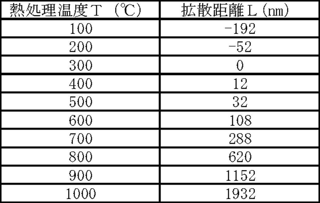
表1に示すように、700℃以上の高温の熱処理温度Tで第三工程の熱処理を行えば、酸素の拡散距離Lが288nm以上となり、第一の絶縁膜24の厚みZを、Z<Lの関係から288nm未満まで厚くすることができ、第一の絶縁膜24だけで保護層28として十分に機能する厚みを確保することができる。なお、保護層28として十分に機能する厚みとしては、活性層18への水分の進入を抑制する観点から30nm以上が好ましく、活性層18からの酸素脱離を抑制する観点から50nm以上がより好ましく、活性層18への水分の進入を回避し且つ活性層18からの酸素脱離を回避する観点から100nm以上がさらに好ましい。また、コストや製造時間を削減する観点から1μm以下が好ましい。
しかしながら、上述したように雰囲気によっては700℃以上の高温となると還元作用が強く働く場合があり、この場合酸素供給量より酸素脱離量の方が増えてしまう。そこで、逆に700℃未満の熱処理温度T、特に600℃未満の低温の熱処理温度Tで第三工程の熱処理を行うことを考えると、酸素の拡散距離Lが288nm未満(700℃未満のとき)、特に108nm未満(600℃未満のとき)となり、熱処理温度Tを低温にすればするほど、第一の絶縁膜24の厚みZを、Z<Lの関係から薄くしなければならない。このように、第一の絶縁膜24の厚みZが薄いと、第一の絶縁膜24だけでは保護層28として十分に機能する厚みを確保することができないので、保護層28として機能する第二の絶縁膜26の成膜が有効となる。
しかしながら、上述したように雰囲気によっては700℃以上の高温となると還元作用が強く働く場合があり、この場合酸素供給量より酸素脱離量の方が増えてしまう。そこで、逆に700℃未満の熱処理温度T、特に600℃未満の低温の熱処理温度Tで第三工程の熱処理を行うことを考えると、酸素の拡散距離Lが288nm未満(700℃未満のとき)、特に108nm未満(600℃未満のとき)となり、熱処理温度Tを低温にすればするほど、第一の絶縁膜24の厚みZを、Z<Lの関係から薄くしなければならない。このように、第一の絶縁膜24の厚みZが薄いと、第一の絶縁膜24だけでは保護層28として十分に機能する厚みを確保することができないので、保護層28として機能する第二の絶縁膜26の成膜が有効となる。
そこで、本実施形態では、第二の絶縁膜26を成膜する第四工程を行う。無論、第一の絶縁膜24だけで保護層28として十分に機能する厚みを確保することができることを前提として、本発明には、第四工程を行わない場合も含むものとする。
-第二の絶縁膜の成膜(第四工程)-
この第四工程では、第三工程後に、図2Gに示すように、第一の絶縁膜24の面上に第二の絶縁膜26を成膜する。
第二の絶縁膜26の成膜方法は、第一の絶縁膜24の成膜方法と同一であってもよいし、異なっていてもよい。ただし、生産性/バリア性の観点から第一の絶縁膜24と第二の絶縁膜26の成膜方法が、共にプラズマを発生する成膜法であることが好ましい。同様に、第二の絶縁膜26の構成材料も、第一の絶縁膜24の構成材料と同一であってもよいし、異なっていてもよい。
なお、第三工程での熱処理温度Tが600℃未満の低温の場合、酸素拡散距離Lが短いため酸素を活性層18界面内部にまで供給するという観点から、第一の絶縁膜24の厚みZを薄くする必要がある。逆に保護層28としては十分に機能しなくなるので、この第四工程では、第一の絶縁膜24を薄くする分、第一の絶縁膜24よりも厚みの大きい第二の絶縁膜26を成膜することが好ましい。
この第四工程では、第三工程後に、図2Gに示すように、第一の絶縁膜24の面上に第二の絶縁膜26を成膜する。
第二の絶縁膜26の成膜方法は、第一の絶縁膜24の成膜方法と同一であってもよいし、異なっていてもよい。ただし、生産性/バリア性の観点から第一の絶縁膜24と第二の絶縁膜26の成膜方法が、共にプラズマを発生する成膜法であることが好ましい。同様に、第二の絶縁膜26の構成材料も、第一の絶縁膜24の構成材料と同一であってもよいし、異なっていてもよい。
なお、第三工程での熱処理温度Tが600℃未満の低温の場合、酸素拡散距離Lが短いため酸素を活性層18界面内部にまで供給するという観点から、第一の絶縁膜24の厚みZを薄くする必要がある。逆に保護層28としては十分に機能しなくなるので、この第四工程では、第一の絶縁膜24を薄くする分、第一の絶縁膜24よりも厚みの大きい第二の絶縁膜26を成膜することが好ましい。
-熱処理(第五工程)-
第四工程後は、必要に応じて、酸化性雰囲気下において第三工程での熱処理温度よりも低い温度で熱処理する第五工程を行う。第三工程での熱処理温度以上の温度で熱処理すると、活性層18中の酸素(第三工程で供給した酸素等)が外部へと拡散してしまう虞があるからである。
第五工程での熱処理温度は、保護層28(第二の絶縁膜26)表面の水分を蒸発させるという観点から100℃以上であることが好ましい。また、保護層28中の水分を蒸発させるという観点から200℃以上であることがより好ましい。
また、第一の絶縁膜24と第二の絶縁膜26の厚みの合計が、上述した保護層28の厚みとなるようにすることが好ましく、例えば活性層18への水分の進入を抑制して保護層28として十分に機能させるという観点から30nm以上であることが好ましい。
第四工程後は、必要に応じて、酸化性雰囲気下において第三工程での熱処理温度よりも低い温度で熱処理する第五工程を行う。第三工程での熱処理温度以上の温度で熱処理すると、活性層18中の酸素(第三工程で供給した酸素等)が外部へと拡散してしまう虞があるからである。
第五工程での熱処理温度は、保護層28(第二の絶縁膜26)表面の水分を蒸発させるという観点から100℃以上であることが好ましい。また、保護層28中の水分を蒸発させるという観点から200℃以上であることがより好ましい。
また、第一の絶縁膜24と第二の絶縁膜26の厚みの合計が、上述した保護層28の厚みとなるようにすることが好ましく、例えば活性層18への水分の進入を抑制して保護層28として十分に機能させるという観点から30nm以上であることが好ましい。
以上の工程を経ることにより、図1Aに示すTFT10を作製することができる。
本発明の実施形態に係るTFT10の製造方法によれば、第一の絶縁膜24の厚みZと熱処理温度Tの調整を行った上で第三工程の熱処理をすることによって、酸化性雰囲気中の酸素を第一の絶縁膜24を介して活性層18の表面内部にまで供給することができるため、第二工程の成膜によって成膜ダメージを受けた活性層18の表面欠陥を十分に補填でき、光照射時のΔVth等の素子特性を顕著に安定化することができる。
なお、TFT10の完成後に、本発明の実施形態に係る製造方法を用いて作製したTFT10であるか否かを確認(第三工程の熱処理を行ったか否かを確認)する手段としては、断面TEM観察、断面TEMとSIMS(Secondary Ion-microprobe Mass Spectrometer:二次イオン質量分析計)の組み合わせ又はICP(Inductively Coupled Plasma:誘導結合プラズマ)発光分析等の組成分析が挙げられる。
具体的に、活性層18と第一の絶縁膜24との区別等を断面TEM観察により行い、さらに活性層18中にZnを含んでいる場合、SIMSによりそのZnが熱処理で拡散して第一の絶縁膜24内に入り込むことが分かっているため、断面TEM観察にて第一の絶縁膜24に相当する領域にZnを表すライン(コントラストの変化も含む)があるか否かを特定する。これにより、第三工程の熱処理を行ったか否かを確認することができる。
又は、活性層18と第一の絶縁膜24との区別等を断面TEM観察により行い、さらに活性層18中にZnを含んでいる場合、SIMSにより第一の絶縁膜24の深さにてZnに対応する強度があるか否かを特定する。これにより、第三工程の熱処理を行ったか否かを確認することができる。
なお、第三工程では上記関係式から300℃超の熱処理温度を必要としているが、Znは酸化性雰囲気の下250℃以上の熱処理によって拡散し始めることが分かっているので、第三工程を行うと必然的に活性層18中のZnが拡散することになる。
また、活性層18中にZnを含んでいる場合で250℃以上の温度で熱処理したとき、Zn元素の減少が観測されため、第三工程で300超の熱処理を施したTFTの活性層18においては、積層膜表面と、積層膜内部にZn元素の減少した部位が見られるはずである。したがって、本発明の実施形態に係る製造方法を用いて作製したTFT10であるか否かは、活性層の組成分布を評価することでも判断できる。
ただし、熱処理が第三工程で行ったものか例えば第五工程で行ったものかを区別することは困難と考えられる。しかし、第三工程での保護層28の厚み(第一の絶縁膜24のみ)と第五工程での保護層28の厚み(第一の絶縁膜24と第二の絶縁膜24)はそれぞれ異なり、また熱処理温度もそれぞれ異なり得るため、Znの拡散量と拡散距離が異なる場合がある。したがって、製造工程にて第三工程と第五工程を両方行っていると、第一の絶縁膜24に相当する領域にZnを表すラインが積層方向にて複数見られるため、第三工程の熱処理を行ったか否かを確認することができるものと考えられる。
また、第五工程を行った場合には、保護層28(特に第二の絶縁膜26)中の水分量が減少しているため、その水分量を熱重量分析等で測定することによって、水分量が多い場合には第三工程を行ったものと特定し、水分量が低い場合には第五工程を行ったものと特定することも可能であると考えられる。
具体的に、活性層18と第一の絶縁膜24との区別等を断面TEM観察により行い、さらに活性層18中にZnを含んでいる場合、SIMSによりそのZnが熱処理で拡散して第一の絶縁膜24内に入り込むことが分かっているため、断面TEM観察にて第一の絶縁膜24に相当する領域にZnを表すライン(コントラストの変化も含む)があるか否かを特定する。これにより、第三工程の熱処理を行ったか否かを確認することができる。
又は、活性層18と第一の絶縁膜24との区別等を断面TEM観察により行い、さらに活性層18中にZnを含んでいる場合、SIMSにより第一の絶縁膜24の深さにてZnに対応する強度があるか否かを特定する。これにより、第三工程の熱処理を行ったか否かを確認することができる。
なお、第三工程では上記関係式から300℃超の熱処理温度を必要としているが、Znは酸化性雰囲気の下250℃以上の熱処理によって拡散し始めることが分かっているので、第三工程を行うと必然的に活性層18中のZnが拡散することになる。
また、活性層18中にZnを含んでいる場合で250℃以上の温度で熱処理したとき、Zn元素の減少が観測されため、第三工程で300超の熱処理を施したTFTの活性層18においては、積層膜表面と、積層膜内部にZn元素の減少した部位が見られるはずである。したがって、本発明の実施形態に係る製造方法を用いて作製したTFT10であるか否かは、活性層の組成分布を評価することでも判断できる。
ただし、熱処理が第三工程で行ったものか例えば第五工程で行ったものかを区別することは困難と考えられる。しかし、第三工程での保護層28の厚み(第一の絶縁膜24のみ)と第五工程での保護層28の厚み(第一の絶縁膜24と第二の絶縁膜24)はそれぞれ異なり、また熱処理温度もそれぞれ異なり得るため、Znの拡散量と拡散距離が異なる場合がある。したがって、製造工程にて第三工程と第五工程を両方行っていると、第一の絶縁膜24に相当する領域にZnを表すラインが積層方向にて複数見られるため、第三工程の熱処理を行ったか否かを確認することができるものと考えられる。
また、第五工程を行った場合には、保護層28(特に第二の絶縁膜26)中の水分量が減少しているため、その水分量を熱重量分析等で測定することによって、水分量が多い場合には第三工程を行ったものと特定し、水分量が低い場合には第五工程を行ったものと特定することも可能であると考えられる。
3.変形例
なお、本発明を特定の実施形態について詳細に説明したが、本発明はかかる実施形態に限定されるものではなく、本発明の範囲内にて他の種々の実施形態が可能であることは当業者にとって明らかであり、例えば上述の複数の実施形態は、適宜、組み合わせて実施可能である。また、以下の変形例同士を、適宜、組み合わせてもよい。
なお、本発明を特定の実施形態について詳細に説明したが、本発明はかかる実施形態に限定されるものではなく、本発明の範囲内にて他の種々の実施形態が可能であることは当業者にとって明らかであり、例えば上述の複数の実施形態は、適宜、組み合わせて実施可能である。また、以下の変形例同士を、適宜、組み合わせてもよい。
例えば、本発明の実施形態に係る半導体素子の製造方法では、第五工程は省略することができる。逆に、第一工程~第五工程以外の工程をさらに有していていもよい。
また、上記実施形態では、一例として、電極形成工程(ゲート電極14、ソース・ドレイン電極20,22)と非電極形成工程(ゲート絶縁層16、活性層18、第一の絶縁膜24、第二の絶縁膜26)は、ゲート電極14がボトムゲート型となる順番で行い、第一の絶縁膜24及び第二の絶縁膜26を半導体膜(活性層18)の保護層28として成膜する場合を説明したが、電極形成工程(ゲート電極14、ソース・ドレイン電極20,22)と非電極形成工程(ゲート絶縁層16、活性層18、第一の絶縁膜24、第二の絶縁膜26)は、図1C又は(D)に示すようにゲート電極14がトップゲート型となる順番で行い、第一の絶縁膜24及び第二の絶縁膜26をゲート絶縁層16として成膜するようにしてもよい。この場合、ゲート絶縁層16の成膜が活性層18にダメージを与えてしまうという問題が発生するからである。
なお、第一の絶縁膜24及び第二の絶縁膜26をゲート絶縁層16として成膜する際には、第一の絶縁膜24及び第二の絶縁膜26の厚みの合計が、上述したゲート絶縁層16の厚み(10nm以上10μm以下が好ましく、50nm以上1000nm以下がより好ましく、100nm以上400nm以下が特に好ましい)となるようにすることが望ましい。
また、上記実施形態では、一例として、電極形成工程(ゲート電極14、ソース・ドレイン電極20,22)と非電極形成工程(ゲート絶縁層16、活性層18、第一の絶縁膜24、第二の絶縁膜26)は、ゲート電極14がボトムゲート型となる順番で行い、第一の絶縁膜24及び第二の絶縁膜26を半導体膜(活性層18)の保護層28として成膜する場合を説明したが、電極形成工程(ゲート電極14、ソース・ドレイン電極20,22)と非電極形成工程(ゲート絶縁層16、活性層18、第一の絶縁膜24、第二の絶縁膜26)は、図1C又は(D)に示すようにゲート電極14がトップゲート型となる順番で行い、第一の絶縁膜24及び第二の絶縁膜26をゲート絶縁層16として成膜するようにしてもよい。この場合、ゲート絶縁層16の成膜が活性層18にダメージを与えてしまうという問題が発生するからである。
なお、第一の絶縁膜24及び第二の絶縁膜26をゲート絶縁層16として成膜する際には、第一の絶縁膜24及び第二の絶縁膜26の厚みの合計が、上述したゲート絶縁層16の厚み(10nm以上10μm以下が好ましく、50nm以上1000nm以下がより好ましく、100nm以上400nm以下が特に好ましい)となるようにすることが望ましい。
ところで、本実施形態では、電極形成工程のうちソース電極20及びドレイン電極22の形成は、ソース電極20及びドレイン電極22がトップコンタクト型となるように第一工程と第二工程の間で行う場合を説明した。この場合、保護層28の成膜による活性層18へのダメージ以外にも、ソース電極20及びドレイン電極22を構成する導電膜の成膜による活性層18へダメージも考慮した方が好ましい。したがって、導電膜の成膜による活性層18へダメージも考慮すると、ソース電極20及びドレイン電極22の厚みをYとしたとき、0<Y<L=8×10⁻⁶×T3-0.0092×T2+3.6×T-468±0.5の関係式を満たすようにソース電極20及びドレイン電極22の厚みと第三工程での熱処理温度を調整することが好ましい。なお、第一の絶縁膜24の厚みZと、ソース電極20及びドレイン電極22の厚みYは、同一であっても異なってもよい。ただし、同一である方が、活性層18の表面欠陥の補填が、第一の絶縁膜24と接する界面と、ソース電極20及びドレイン電極22と接する界面と、において実質的に同等となるので特性制御が容易となるという観点から好ましい。
さらに、ソース電極20及びドレイン電極22の厚みYが、導電性等の観点から足りない場合には、第三工程後にソース電極20及びドレイン電極22用の導電膜を追加成膜するようにしてもよい。
さらに、ソース電極20及びドレイン電極22の厚みYが、導電性等の観点から足りない場合には、第三工程後にソース電極20及びドレイン電極22用の導電膜を追加成膜するようにしてもよい。
一方で、図1Bや図1Dに示すように、電極形成工程のうちソース電極20及びドレイン電極22の形成を、ソース電極20及びドレイン電極22がボトムコンタクト型となるように第一工程よりも前に行うようにすれば、ソース電極20及びドレイン電極22を構成する導電膜の成膜による活性層18へダメージを考慮する必要がない。
なお、日本出願2011-167092の開示はその全体が参照により本明細書に取り込まれる。
本明細書に記載された全ての文献、特許出願、および技術規格は、個々の文献、特許出願、および技術規格が参照により取り込まれることが具体的かつ個々に記載された場合と同程度に、本明細書中に参照により取り込まれる。
なお、日本出願2011-167092の開示はその全体が参照により本明細書に取り込まれる。
本明細書に記載された全ての文献、特許出願、および技術規格は、個々の文献、特許出願、および技術規格が参照により取り込まれることが具体的かつ個々に記載された場合と同程度に、本明細書中に参照により取り込まれる。
4.応用
以上で説明した本実施形態のTFTの用途には特に限定はないが、例えば電気光学装置(例えば液晶表示装置、有機EL(Electro Luminescence)表示装置、無機EL表示装置等の表示装置、等)における駆動素子、特に大面積デバイスに用いる場合に好適である。
更に実施形態のTFTは、樹脂基板を用いた低温プロセスで作製可能なデバイスに特に好適であり(例えばフレキシブルディスプレイ等)、X線センサなどの各種センサ、MEMS(Micro Electro Mechanical System)等、種々の電子デバイスにおける駆動素子(駆動回路)として、好適に用いられるものである。
以上で説明した本実施形態のTFTの用途には特に限定はないが、例えば電気光学装置(例えば液晶表示装置、有機EL(Electro Luminescence)表示装置、無機EL表示装置等の表示装置、等)における駆動素子、特に大面積デバイスに用いる場合に好適である。
更に実施形態のTFTは、樹脂基板を用いた低温プロセスで作製可能なデバイスに特に好適であり(例えばフレキシブルディスプレイ等)、X線センサなどの各種センサ、MEMS(Micro Electro Mechanical System)等、種々の電子デバイスにおける駆動素子(駆動回路)として、好適に用いられるものである。
5.電気光学装置及びセンサ
本実施形態の電気光学装置又はセンサは、前述の本発明の薄膜トランジスタを備えて構成される。
電気光学装置の例としては、表示装置(例えば液晶表示装置、有機EL表示装置、無機EL表示装置、等)がある。
センサの例としては、CCD(Charge Coupled Device)又はCMOS(Complementary Metal Oxide Semiconductor)等のイメージセンサや、X線センサ等が好適である。
本実施形態のTFTを用いた電気光学装置およびセンサは、いずれも特性の面内均一性が高い。なお、ここで言う「特性」とは、電気光学装置(表示装置)の場合には表示特性、センサの場合には感度特性である。
以下、本実施形態によって製造される薄膜トランジスタを備えた電気光学装置又はセンサの代表例として、液晶表示装置、有機EL表示装置、X線センサについて説明する。
本実施形態の電気光学装置又はセンサは、前述の本発明の薄膜トランジスタを備えて構成される。
電気光学装置の例としては、表示装置(例えば液晶表示装置、有機EL表示装置、無機EL表示装置、等)がある。
センサの例としては、CCD(Charge Coupled Device)又はCMOS(Complementary Metal Oxide Semiconductor)等のイメージセンサや、X線センサ等が好適である。
本実施形態のTFTを用いた電気光学装置およびセンサは、いずれも特性の面内均一性が高い。なお、ここで言う「特性」とは、電気光学装置(表示装置)の場合には表示特性、センサの場合には感度特性である。
以下、本実施形態によって製造される薄膜トランジスタを備えた電気光学装置又はセンサの代表例として、液晶表示装置、有機EL表示装置、X線センサについて説明する。
6.液晶表示装置
図3に、本発明の電気光学装置の一実施形態の液晶表示装置について、その一部分の概略断面図を示し、図4にその電気配線の概略構成図を示す。
図3に、本発明の電気光学装置の一実施形態の液晶表示装置について、その一部分の概略断面図を示し、図4にその電気配線の概略構成図を示す。
図3に示すように、本実施形態の液晶表示装置100は、図1Cに示したトップゲート構造でトップコンタクト型のTFT40と、TFT40のパッシベーション層102で保護されたゲート電極14上に画素下部電極104およびその対向上部電極106で挟まれた液晶層108と、各画素に対応させて異なる色を発色させるためのRGBカラーフィルタ110とを備え、TFT40の基板12側およびRGBカラーフィルタ110上にそれぞれ偏光板112a、112bを備えた構成である。
また、図4に示すように、本実施形態の液晶表示装置100は、互いに平行な複数のゲート配線112と、該ゲート配線112と交差する、互いに平行なデータ配線114とを備えている。ここでゲート配線112とデータ配線114は電気的に絶縁されている。ゲート配線112とデータ配線114との交差部付近に、TFT40が備えられている。
TFT40のゲート電極14は、ゲート配線112に接続されており、TFT40のソース電極20はデータ配線114に接続されている。また、TFT40のドレイン電極22はゲート絶縁層16に設けられたコンタクトホール116を介して(コンタクトホール116に導電体が埋め込まれて)画素下部電極104に接続されている。この画素下部電極104は、接地された対向上部電極106とともにキャパシタ118を構成している。
図3に示した本実施形態の液晶装置においては、トップゲート構造のTFT40を備えるものとしたが、本発明の表示装置である液晶装置において用いられるTFTはトップゲート構造に限定されることなく、ボトムゲート構造のTFTであってもよい。
本実施形態のTFTは光照射時の安定性が非常に高いことから、液晶表示装置の信頼性が増す。
7.有機EL表示装置
図5に、本発明の電気光学装置の一実施形態のアクティブマトリックス方式の有機EL表示装置について、その一部分の概略断面図を示し、図6に電気配線の概略構成図を示す。
図5に、本発明の電気光学装置の一実施形態のアクティブマトリックス方式の有機EL表示装置について、その一部分の概略断面図を示し、図6に電気配線の概略構成図を示す。
有機EL表示装置の駆動方式には、単純マトリックス方式とアクティブマトリックス方式の2種類がある。単純マトリックス方式は低コストで作製できるメリットがあるが、走査線を1本ずつ選択して画素を発光させることから、走査線数と走査線あたりの発光時間は反比例する。そのため高精細化、大画面化が困難となっている。アクティブマトリックス方式は画素ごとにトランジスタやキャパシタを形成するため製造コストが高くなるが、単純マトリックス方式のように走査線数を増やせないという問題はないため高精細化、大画面化に適している。
本実施形態のアクティブマトリックス方式の有機EL表示装置200は、図1Cに示したトップゲート構造のTFT40が、パッシベーション層202を備えた基板12上に、駆動用TFT204およびスイッチング用TFT206として備えられ、該TFT204および206上に下部電極208および上部電極210に挟まれた有機発光層212からなる有機EL発光素子214を備え、上面もパッシベーション層216により保護された構成となっている。
また、図6に示すように、本実施形態の有機EL表示装置200は、互いに平行な複数のゲート配線220と、該ゲート配線220と交差する、互いに平行なデータ配線222および駆動配線224とを備えている。ここで、ゲート配線220とデータ配線222、駆動配線224とは電気的に絶縁されている。スイッチング用TFT40bのゲート電極14は、ゲート配線220に接続されており、スイッチング用TFT40bのソース電極20はデータ配線222に接続されている。また、スイッチング用TFT40bのドレイン電極22は駆動用TFT40のゲート電極14に接続されるとともに、キャパシタ226を用いることで駆動用TFT40aをオン状態に保つ。駆動用TFT40aのソース電極20は駆動配線224に接続され、ドレイン電極22は有機EL発光素子214に接続される。
図5に示した本実施形態の有機EL装置においては、トップゲート構造のTFT40aおよび40bを備えるものとしたが、本発明の表示装置である有機EL装置において用いられるTFTは、トップゲート構造に限定されることなく、ボトムゲート構造のTFTであってもよい。
本発明により製造されるTFTは光照射時における安定性が非常に高いことから、信頼性の高い有機EL表示装置の製造に適している。
なお、図5に示した有機EL表示装置において、上部電極210を透明電極としてトップエミッション型としてもよいし、下部電極208およびTFTの各電極を透明電極とすることによりボトムエミッション型としてもよい。
8.X線センサ
図7に、本発明のセンサの一実施形態であるX線センサについて、その一部分の概略断面図を示し、図8にその電気配線の概略構成図を示す。
図7に、本発明のセンサの一実施形態であるX線センサについて、その一部分の概略断面図を示し、図8にその電気配線の概略構成図を示す。
図7は、より具体的にはX線センサアレイの一部を拡大した概略断面図である。本実施形態のX線センサ300は基板12上に形成されたTFT40およびキャパシタ310と、キャパシタ310上に形成された電荷収集用電極302と、X線変換層304と、上部電極306とを備えて構成される。TFT40上にはパッシベーション膜308が設けられている。
キャパシタ310は、キャパシタ用下部電極312とキャパシタ用上部電極314とで絶縁膜316を挟んだ構造となっている。キャパシタ用上部電極314は絶縁膜316に設けられたコンタクトホール318を介し、TFT40のソース電極20およびドレイン電極22のいずれか一方(図7においてはドレイン電極22)と接続されている。
電荷収集用電極302は、キャパシタ310におけるキャパシタ用上部電極314上に設けられており、キャパシタ用上部電極314に接している。
X線変換層304はアモルファスセレンからなる層であり、TFT40およびキャパシタ310を覆うように設けられている。
上部電極306はX線変換層304上に設けられており、X線変換層304に接している。
X線変換層304はアモルファスセレンからなる層であり、TFT40およびキャパシタ310を覆うように設けられている。
上部電極306はX線変換層304上に設けられており、X線変換層304に接している。
図8に示すように、本実施形態のX線センサ300は、互いに平行な複数のゲート配線320と、ゲート配線320と交差する、互いに平行な複数のデータ配線322とを備えている。ここでゲート配線320とデータ配線322は電気的に絶縁されている。ゲート配線320とデータ配線322との交差部付近に、TFT40が備えられている。
TFT40のゲート電極14は、ゲート配線320に接続されており、TFT40のソース電極20はデータ配線322に接続されている。また、TFT40のドレイン電極22は電荷収集用電極302に接続されており、さらにこの電荷収集用電極302は、キャパシタ310に接続されている。
本実施形態のX線センサ300において、X線は図7中、上部(上部電極306側)から照射され、X線変換層304で電子-正孔対を生成する。このX線変換層304に上部電極306によって高電界を印加しておくことにより、生成した電荷はキャパシタ310に蓄積され、TFT40を順次走査することによって読み出される。
本実施形態のX線センサ300は、光照射時の安定性が高いTFT40を備えるため、均一性に優れた画像を得ることができる。
なお、図7に示した本実施形態のX線センサにおいては、トップゲート構造のTFTを備えるものとしたが、本発明のセンサにおいて用いられるTFTはトップゲート構造に限定されることなく、ボトムゲート構造のTFTであってもよい。
9.フォトダイオードの製造方法
以上では、半導体素子の製造方法としてTFTの製造方法を例に挙げて説明したが、半導体素子の製造方法としてフォトダイオードの製造方法についても以下簡単に説明する。
以上では、半導体素子の製造方法としてTFTの製造方法を例に挙げて説明したが、半導体素子の製造方法としてフォトダイオードの製造方法についても以下簡単に説明する。
本発明の実施形態に係るフォトダイオードは、MSM(Metal-Semiconductor-Metal)の櫛型電極を有する横型フォトダイオードであり、図示しないものの、半導体基板上に設定された円形の1つのフォトダイオード領域と、その上に選択エピタキシャル成長により形成された複数(例えば4個)の活性領域と、それらの活性領域に対してそれぞれ設けられ、互いに連絡してそれらの活性領域を電気的に接続する櫛型電極と、それらに接続された電極とから構成されている。
以下、上記構成のフォトダイオードを作製する方法について、図9を参照して説明する。
1)まずSi基板402の表面に、選択エピタキシャル成長のマスクを形成するために、熱酸化によりSiO2層404を形成する。
2)上記SiO2層404をエッチングし、選択エピタキシャル成長する領域する窓領域のSi表面を剥き出しにする(パターニング)。
ここまでの工程を終了した基板402の状態を、図9Aに示す。
2)上記SiO2層404をエッチングし、選択エピタキシャル成長する領域する窓領域のSi表面を剥き出しにする(パターニング)。
ここまでの工程を終了した基板402の状態を、図9Aに示す。
3)適宜クリーニングを行う。
4)LP(UHVが望ましい) CVD装置により低温下(360℃)で選択エピタキシャル成長を行い、酸化物半導体を主体とする半導体膜406を成長させる(膜厚50~100nm)。
5)LP(UHVが望ましい) CVD装置により高温下(700~750℃)で選択エピタキシャル成長を行い、酸化物半導体を主体とする半導体膜406(活性領域)をさらに成長させる(膜厚0.4~1μm)(第一工程)。
6)ファーネス炉により、850℃、30分の条件で熱処理する。
ここまでの工程を終了した基板402の状態を、図9Bに示す。
4)LP(UHVが望ましい) CVD装置により低温下(360℃)で選択エピタキシャル成長を行い、酸化物半導体を主体とする半導体膜406を成長させる(膜厚50~100nm)。
5)LP(UHVが望ましい) CVD装置により高温下(700~750℃)で選択エピタキシャル成長を行い、酸化物半導体を主体とする半導体膜406(活性領域)をさらに成長させる(膜厚0.4~1μm)(第一工程)。
6)ファーネス炉により、850℃、30分の条件で熱処理する。
ここまでの工程を終了した基板402の状態を、図9Bに示す。
7)SiO2層404をデポジションする。
8)SiO2層404に櫛型電極パターンをエッチングする。
9)電極となる金属層をスパッタリング等により形成する。
10)SiO2層404をエッチングして櫛型電極408をパターニングする。
11)パッシベーション層としてSiO2からなる第一の絶縁膜410を成膜する(第二工程)。
ここまでの工程を終了した基板402の状態を、図9Cに示す。
8)SiO2層404に櫛型電極パターンをエッチングする。
9)電極となる金属層をスパッタリング等により形成する。
10)SiO2層404をエッチングして櫛型電極408をパターニングする。
11)パッシベーション層としてSiO2からなる第一の絶縁膜410を成膜する(第二工程)。
ここまでの工程を終了した基板402の状態を、図9Cに示す。
12)図9Dに示すように、ファーネス炉により、酸化性雰囲気下で熱処理する(第三工程)。ここで、第二工程と第三工程の際に、第一の絶縁膜410の厚みをP(nm)とし、第三工程での熱処理温度をT(℃)とし、第一の絶縁膜410及び半導体膜406中への酸素の拡散距離をL(nm)としたとき、0<P<L=8×10⁻⁶×T3-0.0092×T2+3.6×T-468±0.1の関係式を満たすように第一の絶縁膜410の厚みと熱処理温度を調整する。
13)さらなるパッシベーション層としてSiO2からなる第二の絶縁膜412を成膜する(第四工程)。
以上の製造工程を得ることにより、図9Eに示すような本発明の実施形態に係るフォトダイオード400を得ることができる。
以上説明した本発明の実施形態に係るフォトダイオード400の製造方法によれば、第一の絶縁膜410の厚みPと熱処理温度Tの調整を行った上で第三工程の熱処理をすることによって、酸化性雰囲気中の酸素を第一の絶縁膜410を介して半導体膜406の表面内部にまで供給することができるため、第二工程の成膜によって成膜ダメージを受けた半導体膜406の表面欠陥を十分に補填でき、光照射時のΔVth等の素子特性を顕著に安定化することができる。
以下に実施例を説明するが、本発明はこれら実施例により何ら限定されるものではない。
<実験例1:保護層有無によるTFT特性に与える影響の検証>
まず、保護層があるか否かでTFT特性にどのような影響があるのか実験例1により検証した。
まず、保護層があるか否かでTFT特性にどのような影響があるのか実験例1により検証した。
-実験例1-1のサンプル作製-
図10は、実験例1-1のサンプル作製により得られるTFT500の断面図である。
実験例1では、図10に示すように、基板としてゲート電極を兼ねる熱酸化膜504付p型Si基板502(1inch角、厚み:525μmt、熱酸化膜(SiO2):厚み:100nm)を用い、熱酸化膜504をゲート絶縁膜として用いる簡易型のTFT500を作製した(これを実験例1-1のサンプルとする)。
具体的には、レジスト塗布/ベーク、エッチングによる裏面SiO2剥離(BHF使用)、純粋洗浄、レジスト剥離(硫酸過水使用)、純粋洗浄/リンス、N2ブローして作製された熱酸化膜付p型Si基板502を用意する。なお、この基板502はボロンドープで抵抗率:0.001~0.0013Ωcmのものである。
背圧:5×10⁻⁶Pa、成膜圧力:0.8Pa、Ar:30sccm(5.07×10⁻²Pa m3/s)、O2:0.25sccm(4.225×10-4Pa m3/s)、DC:50Wの条件の下、シングルターゲット(豊島製作所製,In:Ga:Zn=1:1:1)を用いて、活性層506としてのIGZO膜(In:Ga:Zn=1:0.9:0.7)を、厚み50nmとしてDCスパッタにより成膜した。なお、通常では活性層506形成後にフォトリソグラフィー及びエッチングによりパターニングを行うが、本発明の効果をより正確に確認するためフォトリソグラフィー及びエッチングでの活性層506界面の汚染やダメージの影響を排除するために、実験例1ではメタルマスクを用いたパターン成膜を行っている。なお、X線回折測定によりこのIGZO膜は非晶質膜であることを確認した。
その後、活性層506(IGZO膜)上に、背圧:4×10⁻⁶Pa、成膜圧力:0.8Pa、Ar:30sccm(5.07×10⁻²Pa m3/s、O2なし)、DC:30Wの条件の下、ソース・ドレイン電極508,510をスパッタにより成膜した。ソース・ドレイン電極510,512の成膜はメタルマスクを用いたパターン成膜にて作製し、Tiを10nm成膜後、Auを40nm成膜した。ソース・ドレイン電極510,512のサイズは各々1mm角とし、電極間距離は0.2mmとした。
図10は、実験例1-1のサンプル作製により得られるTFT500の断面図である。
実験例1では、図10に示すように、基板としてゲート電極を兼ねる熱酸化膜504付p型Si基板502(1inch角、厚み:525μmt、熱酸化膜(SiO2):厚み:100nm)を用い、熱酸化膜504をゲート絶縁膜として用いる簡易型のTFT500を作製した(これを実験例1-1のサンプルとする)。
具体的には、レジスト塗布/ベーク、エッチングによる裏面SiO2剥離(BHF使用)、純粋洗浄、レジスト剥離(硫酸過水使用)、純粋洗浄/リンス、N2ブローして作製された熱酸化膜付p型Si基板502を用意する。なお、この基板502はボロンドープで抵抗率:0.001~0.0013Ωcmのものである。
背圧:5×10⁻⁶Pa、成膜圧力:0.8Pa、Ar:30sccm(5.07×10⁻²Pa m3/s)、O2:0.25sccm(4.225×10-4Pa m3/s)、DC:50Wの条件の下、シングルターゲット(豊島製作所製,In:Ga:Zn=1:1:1)を用いて、活性層506としてのIGZO膜(In:Ga:Zn=1:0.9:0.7)を、厚み50nmとしてDCスパッタにより成膜した。なお、通常では活性層506形成後にフォトリソグラフィー及びエッチングによりパターニングを行うが、本発明の効果をより正確に確認するためフォトリソグラフィー及びエッチングでの活性層506界面の汚染やダメージの影響を排除するために、実験例1ではメタルマスクを用いたパターン成膜を行っている。なお、X線回折測定によりこのIGZO膜は非晶質膜であることを確認した。
その後、活性層506(IGZO膜)上に、背圧:4×10⁻⁶Pa、成膜圧力:0.8Pa、Ar:30sccm(5.07×10⁻²Pa m3/s、O2なし)、DC:30Wの条件の下、ソース・ドレイン電極508,510をスパッタにより成膜した。ソース・ドレイン電極510,512の成膜はメタルマスクを用いたパターン成膜にて作製し、Tiを10nm成膜後、Auを40nm成膜した。ソース・ドレイン電極510,512のサイズは各々1mm角とし、電極間距離は0.2mmとした。
続いて、雰囲気を制御可能な電気炉にて、熱処理を施した。熱処理雰囲気はAr(80%)とO2(20%):1atmの酸化性雰囲気とし、熱処理温度は400℃とし、熱処理時間は1時間とした。
以上により実験例1-1に係るTFT500を作製した。
-実験例1-2のサンプル作製-
次に、実験例1-2のサンプル作製を行った。
図11は、実験例1-2のサンプル作製により得られるTFT600の断面図である。
具体的に、図11に示すように、ソース・ドレイン電極510,512の形成までは、実験例1-1に係るTFT500と同一の方法で行う。そして、ソース・ドレイン電極508,510の形成後は、ソース・ドレイン電極508,510間にある活性層506の露出面上に、背圧:5×10⁻⁶Pa、成膜圧力:0.4Pa、Ar:30sccm(5.07×10⁻²Pa・m3/s)、O2:0.3sccm(5.07×10-4Pa・m3/s)、RF:50Wの条件の下、厚み50nmのGa2O3膜からなる保護層512をRFスパッタにより成膜した。なお、この成膜もメタルマスクを用いたパターン成膜により行っている。
続いて、雰囲気を制御可能な電気炉にて、熱処理を施した。熱処理雰囲気はAr(80%)とO2(20%)で1atmの酸化性雰囲気とし、熱処理温度は400℃とし、熱処理時間は1時間とした。
次に、実験例1-2のサンプル作製を行った。
図11は、実験例1-2のサンプル作製により得られるTFT600の断面図である。
具体的に、図11に示すように、ソース・ドレイン電極510,512の形成までは、実験例1-1に係るTFT500と同一の方法で行う。そして、ソース・ドレイン電極508,510の形成後は、ソース・ドレイン電極508,510間にある活性層506の露出面上に、背圧:5×10⁻⁶Pa、成膜圧力:0.4Pa、Ar:30sccm(5.07×10⁻²Pa・m3/s)、O2:0.3sccm(5.07×10-4Pa・m3/s)、RF:50Wの条件の下、厚み50nmのGa2O3膜からなる保護層512をRFスパッタにより成膜した。なお、この成膜もメタルマスクを用いたパターン成膜により行っている。
続いて、雰囲気を制御可能な電気炉にて、熱処理を施した。熱処理雰囲気はAr(80%)とO2(20%)で1atmの酸化性雰囲気とし、熱処理温度は400℃とし、熱処理時間は1時間とした。
以上により実験例1-2に係るTFT600を作製した。
-実験例1の評価-
実験例1-1に係るTFT500と実験例1-2に係るTFT600にて、バイアスストレスによるΔVthの比較評価を行った。比較評価では、素子サイズはチャネル長180um、チャネル幅1mmとし、VDS(ソースドレイン間電圧)は5V固定で絶えず印加している。ストレス時間にはVg(ゲート電圧)を15V固定し、0~14400秒(0、300、600、1200、1800、2400、3000、3600、5400、7200、10800、14400秒)、計測時にVgを-10~+10V印加し、Vg-Id特性を得た(ストレスフローは図12参照)。Vg-Id特性の計測には半導体パラメータ・アナライザ(アジレントテクノロジー社製)を使用した。計測雰囲気は室温、大気環境下にて行った。
実験例1-1に係るTFT500と実験例1-2に係るTFT600にて、バイアスストレスによるΔVthの比較評価を行った。比較評価では、素子サイズはチャネル長180um、チャネル幅1mmとし、VDS(ソースドレイン間電圧)は5V固定で絶えず印加している。ストレス時間にはVg(ゲート電圧)を15V固定し、0~14400秒(0、300、600、1200、1800、2400、3000、3600、5400、7200、10800、14400秒)、計測時にVgを-10~+10V印加し、Vg-Id特性を得た(ストレスフローは図12参照)。Vg-Id特性の計測には半導体パラメータ・アナライザ(アジレントテクノロジー社製)を使用した。計測雰囲気は室温、大気環境下にて行った。
図13は、実験例1-1に係るTFT500のVg-Id特性の計測結果を示す図である。図14は、実験例1-2に係るTFT600のVg-Id特性の計測結果を示す図である。
図13と図14との比較にて図14の方が、TFT特性が安定していることが分かる。そして、これらの結果からそれぞれΔVth(V)を算出すると、実験例1-1に係るTFT500が4.98V、実験例1-2に係るTFT600が0.66Vとなった。実験例1-1と実験例1-2のサンプルでは保護層512の有無のみの違いしかないので、明らかに保護層が有る方がΔVthの値が小さく、安定している。保護層効果にて雰囲気からの水分や酸素、汚染等の影響を排除できている。つまり、IGZO(酸化物半導体)に保護層512を設けないと動作特性が時間で変化し、実用的には必須であることが確認できた。
<実験例2:保護層成膜による活性層へのダメージの検証>
実験例2以降では、酸化物半導体に必須と確認した保護層を成膜することを前提として、各種実験を行うこととした。
そして、実験例2では、実験例1-1のTFT500の光照射特性と、実験例1-1のTFT500の活性層506の露出面上に、実験例1-2と同一の方法で厚み50nmのGa2O3膜からなる保護層を成膜したきの光照射特性について比較評価して、保護層成膜による活性層へのダメージの検証を行った。
実験例2以降では、酸化物半導体に必須と確認した保護層を成膜することを前提として、各種実験を行うこととした。
そして、実験例2では、実験例1-1のTFT500の光照射特性と、実験例1-1のTFT500の活性層506の露出面上に、実験例1-2と同一の方法で厚み50nmのGa2O3膜からなる保護層を成膜したきの光照射特性について比較評価して、保護層成膜による活性層へのダメージの検証を行った。
光照射特性の評価は、図15に示すように、プローブステージ台700に各TFTを置き、乾燥大気を1時間流した後、当該乾燥大気雰囲気下にてTFT特性(Vg-Id特性)を測定した。モノクロ光照射TFT特性の測定条件は、Vds=10V、モノクロ光源の照射強度を10μW/cm2、波長λの範囲を360~700nmとした。
図16は、光照射特性評価のフローを示す図である。まず、測定対象のTFTは暗い環境下に1時間放置した(素子保管環境下での室内光の影響を排除するため)。TFTにはVg、VDSには電圧印加無しの状態で光照射(キセノンランプを分光にて10uW/cm2)した。照射時間は10minのタイミングでVg、VDSを印加し、光照射を継続しながらVg-Id特性を測定した。ここで、予め、光照射していない時のVg-Id特性からVthを算出しておき、算出したVthを基準として光照射時のVg-Id特性の測定結果から波長毎のΔVthを算出した。なお、測定毎に光照射時の影響を排除するために、1計測(例:500nm)終了したら、光照射していない時のVg-Id特性を再現するまで、暗い環境下で放置した。そして、以上の工程を、全ての計測が終るまで繰り返した。
図17は、実験例1-1のサンプルに対する光照射時のΔVthの算出結果を示す図である。図18は、実験例1-1のサンプルの活性層506の露出面上に、実験例1-2と同一の方法で保護層を成膜したサンプルに対する光照射時のΔVthの算出結果を示す図である。また、表2は、実験例1-1のサンプル(保護層無)に対する光照射時のΔVthと移動度、及び、実験例1-1のサンプルの活性層506の露出面上に、実験例1-2と同一の方法で保護層を成膜したサンプルに対する光照射時のΔVthと移動度をまとめたものである。
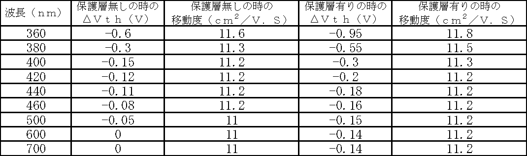
図17、図18及び表2に示す結果から、酸化物半導体に必須と確認した保護層を成膜すると、ΔVthのシフトが生じていることが分かった。特に、短波長側に向かうほどΔVthのシフトがマイナス方向に増大することが分かった。これは、保護層の成膜により活性層506表面がダメージを受けて活性層506の表面欠陥が増大(キャリア増大)したためだと考えられる。
<実験例3:熱処理時の保護層の厚みによる光照射特性の検証>
実験例3では、実験例3-1(比較例1とも呼称する)のサンプルとして実験例1-2と同じTFT600を用い、実験例3-2(実施例1とも呼称する)のサンプルとして以下のようなTFTを用いて、熱処理時の保護層の厚みによる光照射特性の検証を行った。
実験例3では、実験例3-1(比較例1とも呼称する)のサンプルとして実験例1-2と同じTFT600を用い、実験例3-2(実施例1とも呼称する)のサンプルとして以下のようなTFTを用いて、熱処理時の保護層の厚みによる光照射特性の検証を行った。
-実験例3-2のサンプル作製-
図19は、実験例3-2のサンプル作製により得られるTFT800の断面図である。
実験例3-2のサンプル作製では、TFT600の厚み50nmの保護層512を第一の絶縁膜514と第二の絶縁膜516の二層に分け、第一の絶縁膜514の成膜の後に、熱処理を施した。
具体的には、図19に示すように、ソース・ドレイン電極510,512の形成までは、実験例1-1に係るTFT500と同一の方法で行った。そして、ソース・ドレイン電極510,512の形成後は、活性層506の露出面上に、背圧:5×10⁻⁶Pa、成膜圧力:0.4Pa、Ar:30sccm(5.07×10⁻²Pa・m3/s)、O2:0.3sccm(5.07×10-4Pa・m3/s)、RF:50Wの条件の下、厚み10nmのGa2O3膜からなる第一の絶縁膜514をRFスパッタにより成膜した。なお、この成膜もメタルマスクを用いたパターン成膜により行っている。
続いて、雰囲気を制御可能な電気炉にて、熱処理を施した。熱処理雰囲気はAr(80%)とO2(20%)で1atmの酸化性雰囲気とし、熱処理温度は400℃とし、熱処理時間は1時間とした。
熱処理の後、活性層506の露出面上に、第一の絶縁膜514の成膜と同一の条件の下、厚み40nmのGa2O3膜からなる第二の絶縁膜516をRFスパッタにより成膜した。なお、この成膜もメタルマスクを用いたパターン成膜により行っている。
以上により、実験例3-2に係るTFT800を作製した。
図19は、実験例3-2のサンプル作製により得られるTFT800の断面図である。
実験例3-2のサンプル作製では、TFT600の厚み50nmの保護層512を第一の絶縁膜514と第二の絶縁膜516の二層に分け、第一の絶縁膜514の成膜の後に、熱処理を施した。
具体的には、図19に示すように、ソース・ドレイン電極510,512の形成までは、実験例1-1に係るTFT500と同一の方法で行った。そして、ソース・ドレイン電極510,512の形成後は、活性層506の露出面上に、背圧:5×10⁻⁶Pa、成膜圧力:0.4Pa、Ar:30sccm(5.07×10⁻²Pa・m3/s)、O2:0.3sccm(5.07×10-4Pa・m3/s)、RF:50Wの条件の下、厚み10nmのGa2O3膜からなる第一の絶縁膜514をRFスパッタにより成膜した。なお、この成膜もメタルマスクを用いたパターン成膜により行っている。
続いて、雰囲気を制御可能な電気炉にて、熱処理を施した。熱処理雰囲気はAr(80%)とO2(20%)で1atmの酸化性雰囲気とし、熱処理温度は400℃とし、熱処理時間は1時間とした。
熱処理の後、活性層506の露出面上に、第一の絶縁膜514の成膜と同一の条件の下、厚み40nmのGa2O3膜からなる第二の絶縁膜516をRFスパッタにより成膜した。なお、この成膜もメタルマスクを用いたパターン成膜により行っている。
以上により、実験例3-2に係るTFT800を作製した。
-光照射特性の評価-
作製した実験例3-1に係るTFT600と、実験例3-2に係るTFT800に対して、Vg-Id特性やΔVth等の光照射特性の評価を行った。なお、光照射特性の評価は、実験例2と同一の方法を用いて行った。
作製した実験例3-1に係るTFT600と、実験例3-2に係るTFT800に対して、Vg-Id特性やΔVth等の光照射特性の評価を行った。なお、光照射特性の評価は、実験例2と同一の方法を用いて行った。
図20は、実験例3-1に係るTFT600に対するVg-Id特性の計測結果を示す図である。図21は、実験例3-2に係るTFT800に対するVg-Id特性の計測結果を示す図である。
図20の方、つまり実験例3-1:比較例1に係るTFT600は、波長短波側にいくほど、特性シフトが大きくなっていることが分かる。一方、図21の方は、つまり実験例3-2:実施例1に係るTFT800は、TFT600に比べて特性シフトが小さいことが分かった。
図22は、実験例3-1に係るTFT600と実験例3-2に係るTFT800に対するそれぞれの光照射時のΔVthの算出結果を示す図である。
図22から、実験例3-1:比較例1に係るTFT600と実験例3-2:実施例1に係るTFT800の光照射時のΔVthについて、波長:700nmから440nm程度までは共に差はないが、440nmより短波側ではその差が顕著になっていることが分かった。つまり、440nmより短波側で、実験例3-1:比較例1に係るTFT600のΔVthに比べて実験例3-2:実施例1に係るTFT800のΔVthが顕著に改善されている(0Vに近づく)。
これは、実験例3-2:実施例1に係るTFT800の製造方法に関して、第三工程である熱処理時の保護層512の厚み(第一の絶縁膜514の厚みのみ)が10nmと薄いので、第一の絶縁膜514と接する活性層18の界面内部に酸素が供給され、第一の絶縁膜514の成膜により発生した表面欠陥を補填したためと想定できる。
これは、実験例3-2:実施例1に係るTFT800の製造方法に関して、第三工程である熱処理時の保護層512の厚み(第一の絶縁膜514の厚みのみ)が10nmと薄いので、第一の絶縁膜514と接する活性層18の界面内部に酸素が供給され、第一の絶縁膜514の成膜により発生した表面欠陥を補填したためと想定できる。
<実験例4:第三工程の熱処理における酸素拡散深さの検証>
そこで、上記想定した内容を確認するために、第三工程の熱処理にて酸化性雰囲気中の酸素が熱処理温度との関係で、保護層512や活性層506のどの程度深くまで拡散していくのか検証した。
そこで、上記想定した内容を確認するために、第三工程の熱処理にて酸化性雰囲気中の酸素が熱処理温度との関係で、保護層512や活性層506のどの程度深くまで拡散していくのか検証した。
-実験例4に係るサンプル作製-
実験例4に係るサンプル作製では、活性層の形成までは、実験例1-1に係るTFT500と同一の方法で行った。次に、活性層面上に、ソース電極やドレイン電極は形成せずに、そのまま実験例1-2と同一の方法で厚み50nmのGa2O3膜からなる保護層を連続成膜した。そしてこれらの工程を繰り返して、サンプルを4つ用意した。
用意した4つのサンプルに対して、酸素安定同位体であるO18ガス(大陽日酸社の市販18O2ガス)雰囲気の下、300℃、350℃、400℃又は450℃の熱処理温度で加熱処理を行った。酸素安定同位体のO18は通常のO16と実質的に同じ拡散長を有し、保護層や活性層へ拡散していくことが予想される。なお、300℃で熱処理したサンプルを実験例4-1のサンプルとし、350℃で熱処理したサンプルを実験例4-2のサンプルとし、400℃で熱処理したサンプルを実験例4-3のサンプルとし、450℃で熱処理したサンプルを実験例4-4のサンプルと呼称する。
実験例4に係るサンプル作製では、活性層の形成までは、実験例1-1に係るTFT500と同一の方法で行った。次に、活性層面上に、ソース電極やドレイン電極は形成せずに、そのまま実験例1-2と同一の方法で厚み50nmのGa2O3膜からなる保護層を連続成膜した。そしてこれらの工程を繰り返して、サンプルを4つ用意した。
用意した4つのサンプルに対して、酸素安定同位体であるO18ガス(大陽日酸社の市販18O2ガス)雰囲気の下、300℃、350℃、400℃又は450℃の熱処理温度で加熱処理を行った。酸素安定同位体のO18は通常のO16と実質的に同じ拡散長を有し、保護層や活性層へ拡散していくことが予想される。なお、300℃で熱処理したサンプルを実験例4-1のサンプルとし、350℃で熱処理したサンプルを実験例4-2のサンプルとし、400℃で熱処理したサンプルを実験例4-3のサンプルとし、450℃で熱処理したサンプルを実験例4-4のサンプルと呼称する。
なお、熱処理のフローは、実験例1等で説明した熱処理と同様ではあるが、実験例4では酸素安定同位体であるO18を用いるため、より具体的に説明する。
図23は、熱処理時のシステム構成1000を示す図である。
熱処理時のシステム構成1000では、ターボ分子ポンプ1002がメインバルブ1004を介してチャンバー1006に接続されている。チャンバー1006内には、ヒータ1008が配置され、当該ヒータ1008上には熱処理対象のサンプル1010が配置される。そして、チャンバー1006にはさらに、真空ゲージ1012と、マスフローコントローラ1014と、マスフローコントローラ1016とが接続されている。
そして、熱処理では、まずシステム構成1000のチャンバー1006内にあるヒータ1008上にサンプル1010をセットする。そして、メインバルブ1002を開けてターボ分子ポンプ1002を動作し、チャンバー1006内を真空排気する。次に、メインバルブ1004を閉めて、O18ガス真空計で約0.02Paまで導入した。続いて、Arガスを大気圧(0.1MPa)まで導入した。次に、ヒータ1008を昇温速度8℃/minでオンし、目標の温度までサンプルを加熱及び目標温度到達後に30分維持した。最後に、ヒータ1008をオフして室温まで冷却し、サンプルを取り出した。以上にて、熱処理が完了した。そして、上記O18が拡散したサンプルについて以下のSIMS分析を行い、そのO18を検出することで、ある熱処理温度の時にO18元素がどの深さまで拡散したか評価することが出来る。
-SIMS分析-
次に、作製した実験例4-1~実験例4-4のサンプルに対して、SIMS分析を行った。SIMS分析では、具体的にSIMS分析装置としてアルバックファイ株式会社の型式:PHI ADEPT1010を用いた。また、分析環境は、一次イオン種:Cs+、一次加速電圧:3.0kV、検出領域:56×56(μm×μm)とした。また、サンプルからの二次イオンは負極性を検出した。
次に、作製した実験例4-1~実験例4-4のサンプルに対して、SIMS分析を行った。SIMS分析では、具体的にSIMS分析装置としてアルバックファイ株式会社の型式:PHI ADEPT1010を用いた。また、分析環境は、一次イオン種:Cs+、一次加速電圧:3.0kV、検出領域:56×56(μm×μm)とした。また、サンプルからの二次イオンは負極性を検出した。
図24は、実験例4-1のサンプルに対するSIMS分析結果を示す図である。図25は、実験例4-2のサンプルに対するSIMS分析結果を示す図である。図26は、実験例4-3のサンプルに対するSIMS分析結果を示す図である。図27は、実験例4-4のサンプルに対するSIMS分析結果を示す図である。
図24から、実験例4-1のサンプル、つまり300℃の熱処理では、酸素が拡散(保護層等への取り込み)自体していないことが分かった。次に、図25~図27を見ると、熱処理温度が高くなるにつれて、酸素の拡散距離Lが長くなっていることが分かった。
そこで、図24~図27の分析結果に基づいて、各熱処理温度にて18O/(O16+O18)の強度が高くなり始める深さ、つまりO18(=O16)の拡散距離L(nm)を求めて、表3にまとめた。
そこで、図24~図27の分析結果に基づいて、各熱処理温度にて18O/(O16+O18)の強度が高くなり始める深さ、つまりO18(=O16)の拡散距離L(nm)を求めて、表3にまとめた。
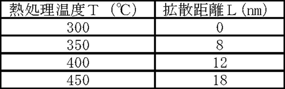
次に、求めた酸素の拡散距離Lと熱処理温度Tの関係をグラフにプロットした。図28は、求めた酸素の拡散距離Lと熱処理温度Tの関係をプロットしたグラフ図である。
そして、図28中のプロットに基づいて、酸素の拡散距離Lと熱処理温度の関係を示す3次関数の近似曲線を算出した。この算出の結果、L=8×10⁻⁶×T3-0.0092×T2+3.6×T-468±0.1という関係式が得られた。なお、「±0.1」は測定(及び算出)誤差であり、図中では、誤差バーで示し、その誤差バーを見やすくするため、「±0.1」より大きく示している。
以上の結果から、例えば熱処理温度が400℃の場合を例に挙げると、図26に示すように、酸化性雰囲気からGa2O3膜へ約12nmまでO18が拡散している(取り込まれている)のが分かる。このことから、実験例3-1では熱処理時の保護層の厚みが50nmであったため、酸素の拡散距離Lとの関係(12nm)で、酸素が活性層界面まで到達していないことが分かった。つまり、保護層成膜(活性層形成も含まれる場合がある)に起因する活性層の表面欠陥は修復できていないものと考えられる。
一方で、実験例3-2では熱処理時の保護層(第一の絶縁膜514)の厚みが10nmであったため、酸素の拡散距離Lとの関係(12nm)で、第一の絶縁膜514と接する活性層界面から2nm程度内部まで酸素が到達していることが分かった。つまり、保護層成膜(活性層形成も含まれる場合がある)に起因する活性層の表面欠陥が修復しているものと考えられる。
一方で、実験例3-2では熱処理時の保護層(第一の絶縁膜514)の厚みが10nmであったため、酸素の拡散距離Lとの関係(12nm)で、第一の絶縁膜514と接する活性層界面から2nm程度内部まで酸素が到達していることが分かった。つまり、保護層成膜(活性層形成も含まれる場合がある)に起因する活性層の表面欠陥が修復しているものと考えられる。
なお、保護層の材料や活性層の材料によって酸素の拡散距離Lが変化してしまうと、上記のような結果とならない虞もあるため、実験例4-5のサンプルとして、活性層の形成まで実験例1-1に係るTFT500と同一の方法で行い、次に実験例4-4と同一の熱処理条件(熱処理温度は400℃)にて熱処理を行うことにより作製し、保護層は形成せずそのままSIMS分析を行った。
図29は、実験例4-5のサンプルに対するSIMS分析結果を示す図である。
図29に示す結果から、酸化性雰囲気からIGZO膜(活性層)へ約12nmまでO18が拡散している(取り込まれている)のが分かる。そして、この結果は、酸化性雰囲気からGa2O3膜へ約12nmまでO18が拡散する実験例4-4の場合と同一の結果であることが分かった。したがって、保護層や活性層の材料が異なっても酸素の拡散距離Lは変わらないものと考えられる。また、保護層や活性層の成膜方法によっても酸素の拡散距離Lは変わらないことを確認している。例えば、スパッタ法においてシングルターゲットを用いる方法を用いても、共スパッタ法を用いても酸素の拡散距離Lは変わらなかった。
また、以上の考察、結論及び表3に示す結果から、第一の絶縁膜514の厚みZが、Z<L=8×10⁻⁶×T3-0.0092×T2+3.6×T-468±0.1という関係式を満たせば、第一の絶縁膜514と接する活性層界面内部まで酸素が到達するものと結論付けた。なお、上記関係式においてZ=Lを含まないのは、酸素が活性層界面に到達するだけでは活性層内部にある表面欠陥が十分に修復できないものと想定できるからである。
<実験例5:修復程度の検証>
そこで、上記想定した内容を確認するために、熱処理条件を固定(熱処理温度は400℃で固定)して、保護層(第一の絶縁膜514)の厚みによって、どのように活性層内部にある表面欠陥が修復していくのか、各第一の絶縁膜514の厚みにおけるΔVthと移動度を求めることにより検証した。
そこで、上記想定した内容を確認するために、熱処理条件を固定(熱処理温度は400℃で固定)して、保護層(第一の絶縁膜514)の厚みによって、どのように活性層内部にある表面欠陥が修復していくのか、各第一の絶縁膜514の厚みにおけるΔVthと移動度を求めることにより検証した。
-実験例5に係るサンプルの作製-
実験例5に係るサンプルの作製では、実験例3-2のサンプル作製と同一の方法を用い、第二の絶縁膜516の厚みを20nmと固定し、第一の絶縁膜514の厚みのみを、8nm、10nm、11nm、12nm、20nm、50nmと変化させて、図19に示すようなTFTサンプルを作製した。なお、第一の絶縁膜514の厚みを8nmとしたサンプルを実験例5-1(実施例2とも呼称する)に係るサンプルとし、第一の絶縁膜514の厚みを10nmとしたサンプルを実験例5-2(実施例3とも呼称する)に係るサンプルとし、第一の絶縁膜514の厚みを11nmとしたサンプルを実験例5-3(実施例4とも呼称する)に係るサンプルとし、第一の絶縁膜514の厚みを12nmとしたサンプルを実験例5-4(比較例2とも呼称する)に係るサンプルとし、第一の絶縁膜514の厚みを20nmとしたサンプルを実験例5-5(比較例3とも呼称する)に係るサンプルとし、第一の絶縁膜514の厚みを50nmとしたサンプルを実験例5-6(比較例4とも呼称する)に係るサンプルと呼称する。
実験例5に係るサンプルの作製では、実験例3-2のサンプル作製と同一の方法を用い、第二の絶縁膜516の厚みを20nmと固定し、第一の絶縁膜514の厚みのみを、8nm、10nm、11nm、12nm、20nm、50nmと変化させて、図19に示すようなTFTサンプルを作製した。なお、第一の絶縁膜514の厚みを8nmとしたサンプルを実験例5-1(実施例2とも呼称する)に係るサンプルとし、第一の絶縁膜514の厚みを10nmとしたサンプルを実験例5-2(実施例3とも呼称する)に係るサンプルとし、第一の絶縁膜514の厚みを11nmとしたサンプルを実験例5-3(実施例4とも呼称する)に係るサンプルとし、第一の絶縁膜514の厚みを12nmとしたサンプルを実験例5-4(比較例2とも呼称する)に係るサンプルとし、第一の絶縁膜514の厚みを20nmとしたサンプルを実験例5-5(比較例3とも呼称する)に係るサンプルとし、第一の絶縁膜514の厚みを50nmとしたサンプルを実験例5-6(比較例4とも呼称する)に係るサンプルと呼称する。
-光照射特性の評価-
次に、作製した実験例5-1~5-6に係るサンプルに対して、Vg-Id特性の測定を行ってΔVthや移動度を求める等して光照射特性の評価を行った。なお、光照射特性の評価は、実験例2と同一の方法を用いて行った。
次に、作製した実験例5-1~5-6に係るサンプルに対して、Vg-Id特性の測定を行ってΔVthや移動度を求める等して光照射特性の評価を行った。なお、光照射特性の評価は、実験例2と同一の方法を用いて行った。
図30は、実験例5-1~5-6に係るサンプルに対する光照射波長とΔVthの関係を示す図である。
図30に示す結果から、第一の絶縁膜514の厚みが50nmから8nmにかけて薄くなればなるほどΔVthが低減(改善)しており、そして特に光照射の波長が短波長になればなるほど、そのΔVthの改善度合いが高まっている。
ここで、実験例4で検証したように、酸素の拡散距離Lとの関係(熱処理温度400℃のとき12nm)で酸素が活性層界面内部にまで到達していないはずの、実験例5-3~5-5のサンプルもΔVthが改善していることが問題となるようにも思われる。つまり、酸化性雰囲気中の酸素が第一の絶縁膜514を介して活性層界面内部にまで到達しているか否かで、活性層内部にある表面欠陥を修復できるか否かを想定したことが誤りではないかということが問題となるようにも思われる。
そこで、図30のプロットを第一の絶縁膜514の厚みZとΔVthの関係にし直した。図31は、実験例5-1~5-6に係るサンプルに対する第一の絶縁膜514の厚みZと光照射時のΔVthの関係を示す図である。また、以上の評価で求めた各サンプルのΔVthと移動度の各値を表4~表6にまとめた。
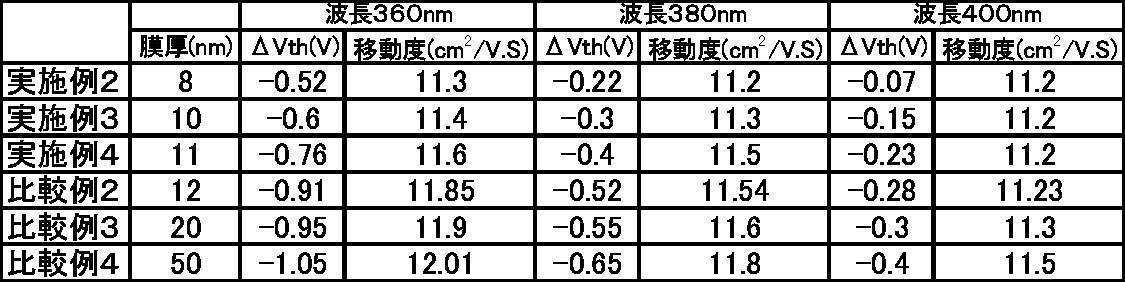


図31並びに表4~表6に示す結果から、実験例4で検証したように、酸素の拡散距離Lとの関係(熱処理温度400℃のとき12nm)で酸素が活性層界面内部にまで到達していないはずの、実験例5-4~5-6のサンプル(第一の絶縁膜514の厚みZ=12、20、50の所謂比較例2~4のサンプル)では、その範囲内で第一の絶縁膜514の厚みZが薄くなっても、ΔVthはほとんど改善していないことが分かった。例えば、厚み1nm当り薄くしてもΔVthが小数点第3桁~4桁程度しか改善しない。そして、これは光照射の波長を変化しても同じ結論となることが分かる。
一方で、第一の絶縁膜514の厚みZが12nmを境界として、実験例5-1~5-3のサンプル(第一の絶縁膜514の厚みZ=8、10、11の所謂実施例2~4のサンプル)では、その範囲内で第一の絶縁膜514の厚みZを薄くしていくと急激にΔVthが改善していることが分かった。厚み1nm当り薄くするとΔVthが小数点第1桁~2桁程度顕著に改善する(0Vに近づく)。特に、波長400nm以下の短波長の光照射をする場合、1nm当りでΔVthが小数点第1桁程度改善することになり、急激さ(顕著さ)が増す。
具体的に、波長400nmの短波長の光照射をする場合、第一の絶縁膜514の厚みが12nm以上であると1nm当りのΔVthの改善度が約0.003(V/nm)でしかないものが、第一の絶縁膜514の厚みが12nm未満であると約0.16(V/nm)に飛躍的に改善する。
なお、波長700nm以上の光照射を行う場合は、第一の絶縁膜514の厚みZが上記範囲内(Z=8、10、11)では、ΔVthが負の値から0を超え正の値となってしまうことから、波長700nm未満の光照射を行うようにすることが好ましいことが分かった。
一方で、第一の絶縁膜514の厚みZが12nmを境界として、実験例5-1~5-3のサンプル(第一の絶縁膜514の厚みZ=8、10、11の所謂実施例2~4のサンプル)では、その範囲内で第一の絶縁膜514の厚みZを薄くしていくと急激にΔVthが改善していることが分かった。厚み1nm当り薄くするとΔVthが小数点第1桁~2桁程度顕著に改善する(0Vに近づく)。特に、波長400nm以下の短波長の光照射をする場合、1nm当りでΔVthが小数点第1桁程度改善することになり、急激さ(顕著さ)が増す。
具体的に、波長400nmの短波長の光照射をする場合、第一の絶縁膜514の厚みが12nm以上であると1nm当りのΔVthの改善度が約0.003(V/nm)でしかないものが、第一の絶縁膜514の厚みが12nm未満であると約0.16(V/nm)に飛躍的に改善する。
なお、波長700nm以上の光照射を行う場合は、第一の絶縁膜514の厚みZが上記範囲内(Z=8、10、11)では、ΔVthが負の値から0を超え正の値となってしまうことから、波長700nm未満の光照射を行うようにすることが好ましいことが分かった。
以上の結果から、熱処理温度Tとの関係で第一の絶縁膜514の厚みZを調整しなくとも(厚みZが厚くても)、少なくとも300℃超の熱処理によって、酸化性雰囲気中の酸素ではなく第一の絶縁膜514中の酸素又第一の絶縁膜514以外(側面等)を介した酸素を、当該第一の絶縁膜24と接する活性層18の界面内部に供給することによっても、光照射時のΔVthを改善(TFT特性の安定化)することができるものの、その改善はごく僅かなものであるということが分かった。そして、上記で問題提起したように、酸化性雰囲気中の酸素が第一の絶縁膜514を介して活性層界面内部にまで到達しているか否かで、活性層内部にある表面欠陥を修復できるか否かを想定したことが誤りではないかという問題に対しては、酸化性雰囲気中の酸素が第一の絶縁膜514を介して活性層界面(丁度)に到達するL=Z=12の条件を満たす実験例5-4:比較例2のサンプルを境として、ΔVthの改善度合いが明らかに異なることから、酸化性雰囲気中の酸素が第一の絶縁膜514を介して活性層界面内部にまで到達しているか否かで、活性層内部にある表面欠陥を十分に修復できるか否かが変わるという結論に至った。
さらに、熱処理温度Tを400℃に固定したが、他の熱処理温度でも上記結論は変わらないものと考えられるので、最終的に、第一の絶縁膜514の厚みをZ(nm)とし、第三工程での熱処理温度をT(℃)とし、さらに酸素の拡散距離をL(nm)としたとき、0<Z<L=8×10⁻⁶×T3-0.0092×T2+3.6×T-468±0.1の関係式を満たすように第一の絶縁膜514の厚みと熱処理温度を調整すれば、酸化性雰囲気中の酸素を第一の絶縁膜を介して活性層の表面内部にまで供給することができることとなり、第二工程の成膜によって成膜ダメージを受けた活性層の表面欠陥を十分に補填でき、光照射時のΔVth等の素子特性を顕著に安定化することができる、という結論を得た。
さらに、熱処理温度Tを400℃に固定したが、他の熱処理温度でも上記結論は変わらないものと考えられるので、最終的に、第一の絶縁膜514の厚みをZ(nm)とし、第三工程での熱処理温度をT(℃)とし、さらに酸素の拡散距離をL(nm)としたとき、0<Z<L=8×10⁻⁶×T3-0.0092×T2+3.6×T-468±0.1の関係式を満たすように第一の絶縁膜514の厚みと熱処理温度を調整すれば、酸化性雰囲気中の酸素を第一の絶縁膜を介して活性層の表面内部にまで供給することができることとなり、第二工程の成膜によって成膜ダメージを受けた活性層の表面欠陥を十分に補填でき、光照射時のΔVth等の素子特性を顕著に安定化することができる、という結論を得た。
また、図31並びに表4~表6に示す結果から、熱処理温度Tが400℃のとき第一の絶縁膜514の厚みZを11nm以下に調整する、すなわち、Z≦(L-1.0)=8×10⁻⁶×T3-0.0092×T2+3.6×T-468±0.1-1.0の関係式を満たすように第一の絶縁膜514の厚みと熱処理温度を調整することが好ましいことが分かる。第一の絶縁膜514の厚みを上記範囲内で薄くするとΔVthがより顕著に改善し且つ光照射の波長が360nm以上のどの波長であっても、ΔVthが-0.8V超に改善するからである。
さらに、図31並びに表4~表6に示す結果から、熱処理温度Tが400℃のとき第一の絶縁膜514の厚みZを10nm以下に調整する、すなわち、Z≦(L-2.0)=8×10⁻⁶×T3-0.0092×T2+3.6×T-468±0.1-2.0の関係式を満たすように第一の絶縁膜24の厚みと熱処理温度を調整することが好ましい。光照射の波長が360nm以上のどの波長であっても、ΔVthが-0.6V以上に改善するからである。
次に、図32は、実験例5-1:実施例2~5-6:比較例4に係るサンプルに対する第一の絶縁膜514の厚みZと光照射時の移動度の関係を示す図である。
図32及び表4~表6から移動度に関しては、420nm未満の短波では、ΔVthとは逆に第一の絶縁膜514の厚みZが12nmであるときを境として、それよりも薄くなると急激に悪化していることが分かる。これは、キャリアとして働いていた活性層の表面欠陥が、第一の絶縁膜514を介して活性層界面内部に酸素が供給されることにより、補填された証拠となる。
図32及び表4~表6から移動度に関しては、420nm未満の短波では、ΔVthとは逆に第一の絶縁膜514の厚みZが12nmであるときを境として、それよりも薄くなると急激に悪化していることが分かる。これは、キャリアとして働いていた活性層の表面欠陥が、第一の絶縁膜514を介して活性層界面内部に酸素が供給されることにより、補填された証拠となる。
このように移動度の減少が顕著になるとTFTとして好ましくないので、これを回避するために、熱処理温度400℃のとき少なくとも第一の絶縁膜の厚み514を7nm以上に調整する、すなわち、(L-5.0)=8×10⁻⁶×T3-0.0092×T2+3.6×T-468±0.1-5.0≦Zの関係式を満たすように第一の絶縁膜514の厚みと熱処理温度を調整することが好ましいことが分かった。
また、420nm以上の長波長では、第一の絶縁膜514の厚みZが10nm又は11nmのときが移動度急激減少の境界となっている。したがって、熱処理温度400℃のとき少なくとも10nm以上に調整する、すなわち、(L-2.0)=8×10⁻⁶×T3-0.0092×T2+3.6×T-468±0.1-2.0≦Zの関係式を満たすように第一の絶縁膜514の厚みと熱処理温度を調整することが好ましいことが分かった。長波長の光照射では、活性層の移動度がほぼ変化(減少)しないからである。
また、波長を変えてもより移動度が変化しないという理由から、熱処理温度400℃のとき少なくとも11nm以上に調整する、すなわち、(L-1.0)=8×10⁻⁶×T3-0.0092×T2+3.6×T-468±0.1-2.0≦Zの関係式を満たすように第一の絶縁膜514の厚みと熱処理温度を調整することがより好ましい。
また、波長を変えてもより移動度が変化しないという理由から、熱処理温度400℃のとき少なくとも11nm以上に調整する、すなわち、(L-1.0)=8×10⁻⁶×T3-0.0092×T2+3.6×T-468±0.1-2.0≦Zの関係式を満たすように第一の絶縁膜514の厚みと熱処理温度を調整することがより好ましい。
さらに、第一の絶縁膜514成膜直後に400℃で熱処理した表4~表6と、活性層形成直後に400℃で熱処理して第一の絶縁膜514等の保護層を成膜しない結果を示す表2を比較すると、第一の絶縁膜514の厚みZを10nmにして熱処理したときのΔVthが、活性層形成直後に400℃で熱処理したときのΔVthと実質的に同等となっていることが分かる。つまり、第一の絶縁膜514を成膜したとき生成した表面欠陥を実質的に100%補填していることが分かる。さらに言えば、第一の絶縁膜514の厚みZを8nmにして熱処理したときのΔVthは、むしろ活性層形成直後に400℃で熱処理したときのΔVthよりも改善していることが分かる。これは、活性層形成時に生成した表面欠陥までも酸素供給により補填したためだと考えられる。
<実験例6:Zn拡散の検証>
最後に、TFT完成後に、本発明の実施例に係る製造方法(0<Z<L=8×10⁻⁶×T3-0.0092×T2+3.6×T-468±0.1の関係式を満たすように第一の絶縁膜514の厚みと熱処理温度を調整)を用いて作製したTFTであるか否かを確認する手段としては、Znの拡散に基づく確認手段が想定できる。なぜなら、Siノンドープ基板上にIGZO膜を200nm成膜したサンプルについて、IGZO中のZn(M/Z64)が250℃以上の低温で拡散するという事実を、昇温脱離分析により見出したからである(図33参照)。
最後に、TFT完成後に、本発明の実施例に係る製造方法(0<Z<L=8×10⁻⁶×T3-0.0092×T2+3.6×T-468±0.1の関係式を満たすように第一の絶縁膜514の厚みと熱処理温度を調整)を用いて作製したTFTであるか否かを確認する手段としては、Znの拡散に基づく確認手段が想定できる。なぜなら、Siノンドープ基板上にIGZO膜を200nm成膜したサンプルについて、IGZO中のZn(M/Z64)が250℃以上の低温で拡散するという事実を、昇温脱離分析により見出したからである(図33参照)。
そこで、IGZOのZnがIGZO膜と接する他の層にまで拡散するか否かSIMS分析を用いて検証した。この分析のサンプルとしては、具体的には、図19に示すように、活性層となるIGZO膜の形成までは、実験例1-1に係るTFT500と同一の方法で行い、ソース電極やドレイン電極は形成せずに、そのまま保護層となる厚み100nmのGa2O3膜を成膜したものを用いた。そして、熱処理の有り無しで、SIMS分析をそれぞれ行った。なお、分析方法の詳細は、実験例4と同様なので省略する。
図34は、SIMS分析によるInの深さと二次イオン強度を示す図である。図35は、SIMS分析によるZnの深さと二次イオン強度を示す図である。
図34に示す結果から、IGZO膜中のInは、熱処理が有ってもGa2O3膜まではほぼ拡散していないことが分かる。一方で、IGZO膜中のZnは、熱処理が有るとGa2O3膜中まで拡散していることが分かる。
以上の結果から、TFT完成後に、本発明の実施例に係る製造方法(0<Z<L=8×10⁻⁶×T3-0.0092×T2+3.6×T-468±0.1の関係式を満たすように第一の絶縁膜514の厚みと熱処理温度を調整)を用いて作製したTFTであるか否かを確認する手段としては、Znの拡散に基づく確認手段が有効であると考えられ、例えば断面TEM観察にて第一の絶縁膜514に相当する領域にZnを表すライン(コントラストの変化も含む)があるか否かを特定する手段等が挙げられる。
<実験例7:他の材料への関係式の適用性の検証>
次に、上述した「保護層の材料が異なっても酸素の拡散距離Lは変わらないものと考えられる」という点について検証する。すなわち、第一の絶縁膜がGa2O3膜でなくても、他の材料、例えば金属酸化物であっても、図28に基づく上記の関係式「L=8×10⁻⁶×T3-0.0092×T2+3.6×T-468±0.1」がそのまま当てはめられるか検証した。
次に、上述した「保護層の材料が異なっても酸素の拡散距離Lは変わらないものと考えられる」という点について検証する。すなわち、第一の絶縁膜がGa2O3膜でなくても、他の材料、例えば金属酸化物であっても、図28に基づく上記の関係式「L=8×10⁻⁶×T3-0.0092×T2+3.6×T-468±0.1」がそのまま当てはめられるか検証した。
図36は、Ga2O3膜を含む実験例4-3のサンプルに対するSIMS分析結果とIGZO膜(In:Ga:Zn=1:0.9:0.7)を含む実験例4-5のサンプルに対するSIMS分析結果を示す図である。
また、図37は、In,Ga,Znの組成比がIn:Ga:Zn=1.85:0.15:1, In:Ga:Zn=1:1:1, In:Ga:Zn=0.5:1.5:1の3つのIGZO膜を、それぞれ実験例4-3と同一の条件(ただし、熱処理温度は450℃)で熱処理した各サンプルに対するSIMS分析結果を示す図である。
さらに、図38は、組成比がIn:Ga:Zn=0.5:1.5:1のIGZO膜を実験例4-3と同一の条件(ただし、熱処理温度は450℃)で熱処理したサンプルに対するSIMS分析結果と、SiO2膜を実験例4-3と同一の条件(ただし、熱処理温度は450℃)で熱処理したサンプルに対するSIMS分析結果を示す図である。
なお、図37及び図38に係る各サンプルに対するSIMS分析は、上述したSIMS分析と同一の方法を用いて行っている。
さらに、図38は、組成比がIn:Ga:Zn=0.5:1.5:1のIGZO膜を実験例4-3と同一の条件(ただし、熱処理温度は450℃)で熱処理したサンプルに対するSIMS分析結果と、SiO2膜を実験例4-3と同一の条件(ただし、熱処理温度は450℃)で熱処理したサンプルに対するSIMS分析結果を示す図である。
なお、図37及び図38に係る各サンプルに対するSIMS分析は、上述したSIMS分析と同一の方法を用いて行っている。
図36に示すSIMS分析結果から、「Ga2O3中」に係る実験データと「IGZO中」に係る実験データの間で、18O/(16O+18O)の割合は異なるものの、18O/(16O+18O)の割合が一定となり始める表面からの距離は同じであることが分かる。すなわち、各実験データから、Ga2O3膜に対する18O(=16O)の拡散距離Lと、IGZO膜(In:Ga:Zn=1:0.9:0.7)に対する18O(=16O)の拡散距離Lは、同じ12nmであることが分かった。
この実験事実から、Ga2O3膜とIGZO膜は酸素の拡散距離Lが同じであり、この拡散距離Lは「L=8×10⁻⁶×T3-0.0092×T2+3.6×T-468±0.1」で表されるという結論が得られた。
この実験事実から、Ga2O3膜とIGZO膜は酸素の拡散距離Lが同じであり、この拡散距離Lは「L=8×10⁻⁶×T3-0.0092×T2+3.6×T-468±0.1」で表されるという結論が得られた。
また、図37に示すSIMS分析結果から、IGZO中のIn,Ga,Znの組成比がIn:Ga:Zn=1.85:0.15:1, In:Ga:Zn=1:1:1, In:Ga:Zn=0.5:1.5:1と変化しても、18O/(16O+18O)の割合が一定となり始める表面からの距離Lは同じ18nmであることが分かった。
この実験事実から、IGZO膜はその組成比が変わっても酸素の拡散距離Lが同じであり、この拡散距離Lは「L=8×10⁻⁶×T3-0.0092×T2+3.6×T-468±0.1」で表されるという結論が得られた。
この実験事実から、IGZO膜はその組成比が変わっても酸素の拡散距離Lが同じであり、この拡散距離Lは「L=8×10⁻⁶×T3-0.0092×T2+3.6×T-468±0.1」で表されるという結論が得られた。
さらに、図38に示すSIMS分析結果から、「IGZO(0.5:1.5:1)」に係る実験データと「SiO2」に係る実験データの間で、18O/(16O+18O)の割合は異なるものの、18O/(16O+18O)の割合が一定となり始める表面からの距離は同じであることが分かった。すなわち、各実験データから、SiO2膜に対する18Oの拡散距離Lと、IGZO膜(In:Ga:Zn=0.5:1.5:1)に対する18O(=16O)の拡散距離Lは、同じ18nmであることが分かった。
以上、図36~図38全ての実験事実を組み合わせれば、18O、すなわち酸素の拡散距離Lは、SiO2やIGZO,Ga2O3等の材料、特に金属酸化物であれば変化せず(違いはなく)、上記関係式が「L=8×10⁻⁶×T3-0.0092×T2+3.6×T-468±0.1」で表されるという結論が得られた。
すなわち、Ga2O3膜における酸素の拡散距離Lが「L=8×10⁻⁶×T3-0.0092×T2+3.6×T-468±0.1」で表された場合、第一の絶縁膜がGa2O3以外の他の材料で構成されていても、上記の関係式がそのまま当てはめられるという結論が得られた。
すなわち、Ga2O3膜における酸素の拡散距離Lが「L=8×10⁻⁶×T3-0.0092×T2+3.6×T-468±0.1」で表された場合、第一の絶縁膜がGa2O3以外の他の材料で構成されていても、上記の関係式がそのまま当てはめられるという結論が得られた。
Claims (24)
- 酸化物半導体を主体とする半導体膜を成膜する第一工程と、
前記第一工程後に、前記半導体膜の面上に第一の絶縁膜を成膜する第二工程と、
前記第二工程後に、酸化性雰囲気中で熱処理する第三工程と、
前記第三工程後に、前記第一の絶縁膜の面上に第二の絶縁膜を成膜する第四工程と、
を有し、
前記第二工程と前記第三工程の際に、前記第一の絶縁膜の厚みをZ(nm)とし、前記第三工程での熱処理温度をT(℃)とし、前記第一の絶縁膜及び前記半導体膜中への酸素の拡散距離をL(nm)としたとき、0<Z<L=8×10⁻⁶×T3-0.0092×T2+3.6×T-468±0.1の関係式を満たすように前記第一の絶縁膜の厚みと前記熱処理温度を調整する半導体素子の製造方法。 - 前記第二工程と前記第三工程の際に、Z≦L-1.0の関係式を満たすように前記第一の絶縁膜の厚みと前記熱処理温度を調整する、
請求項1に記載の半導体素子の製造方法。 - 前記第二工程と前記第三工程の際に、Z≦L-2.0の関係式を満たすように前記第一の絶縁膜の厚みと前記熱処理温度を調整する、
請求項2に記載の半導体素子の製造方法。 - 前記第二工程と前記第三工程の際に、L-5.0≦Zの関係式を満たすように前記第一の絶縁膜の厚みと前記熱処理温度を調整する、
請求項1~請求項3の何れか1項に記載の半導体素子の製造方法。 - 前記第二工程と前記第三工程の際に、L-2.0≦Zの関係式を満たすように前記第一の絶縁膜の厚みと前記熱処理温度を調整する、
請求項1又は請求項2に記載の半導体素子の製造方法。 - 前記第二工程の際に、前記第一の絶縁膜の厚みZを、2nm以上に調整する、
請求項1~請求項5の何れか1項に記載の半導体素子の製造方法。 - 前記第二工程と前記第四工程の際に、プラズマを発生する成膜法を用いて前記第一の絶縁膜及び前記第二の絶縁膜を成膜する、
請求項1~請求項6の何れか1項に記載の半導体素子の製造方法。 - 前記第二工程では、前記第四工程での成膜よりも成膜速度を下げ且つブラズマ電位を下げる、又は成膜圧力を上げる、
請求項7に記載の半導体素子の製造方法。 - 前記第二工程では、前記第一の絶縁膜を20nm/min以下の成膜速度で成膜する、
請求項7又は請求項8に記載の半導体素子の製造方法。 - 前記第二工程では、前記第四工程で前記第二の絶縁膜を成膜する成膜時間よりも短い成膜時間で前記第一の絶縁膜を成膜する、
請求項7~請求項9の何れか1項に記載の半導体素子の製造方法。 - 前記第一工程では、前記半導体膜の厚みが5nm以上となるように成膜する、
請求項1~請求項10の何れか1項に記載の半導体素子の製造方法。 - 前記第四工程後に、酸化性雰囲気下において前記第三工程での熱処理温度よりも低い温度で熱処理する第五工程、
をさらに有する請求項1~請求項11の何れか1項に記載の半導体素子の製造方法。 - 前記第五工程の熱処理温度は、100℃以上である、
請求項12に記載の半導体素子の製造方法。 - 前記第五工程の熱処理温度は、300℃以上である、
請求項13に記載の半導体素子の製造方法。 - 前記第四工程では、前記第一の絶縁膜よりも厚みの大きい前記第二の絶縁膜を成膜する、
請求項1~請求項14の何れか1項に記載の半導体素子の製造方法。 - 前記酸化物半導体は、In、Ga及びZnのうちの少なくとも1種を含む非晶質酸化物である、
請求項1~請求項15の何れか1項に記載の半導体素子の製造方法。 - 前記第三工程での前記熱処理温度を、600℃未満とする、
請求項1~請求項16の何れか1項に記載の半導体素子の製造方法。 - 前記第二工程では、前記半導体膜の面上全面に前記第一の絶縁膜を成膜する、
請求項1~請求項17の何れか1項に記載の半導体素子の製造方法。 - 前記第二の絶縁膜の構成材料は、金属を含み、
前記第一の絶縁膜は、前記第二の絶縁膜の構成材料の少なくとも一部の金属と前記半導体膜の構成材料の少なくとも一部の金属との両方を含む、
請求項1~請求項18の何れか1項に記載の半導体素子の製造方法。 - ゲート電極、ソース電極、及びドレイン電極を形成する電極形成工程と、
前記電極形成工程の前又は間に、請求項1~請求項19の何れか1項に記載の半導体素子の製造方法を用いて活性層としての前記半導体膜並びに前記半導体膜の保護層又はゲート絶縁層としての前記第一の絶縁膜及び前記第二の絶縁膜を成膜する非電極形成工程と、
を有する電界効果型トランジスタの製造方法。 - 前記電極形成工程と前記非電極形成工程は、前記ゲート電極がボトムゲート型となる順番で行い、前記第一の絶縁膜及び前記第二の絶縁膜を前記半導体膜の保護層として成膜する、
請求項20に記載の電界効果型トランジスタの製造方法。 - 前記第一の絶縁膜と前記第二の絶縁膜の厚みの合計が30nm以上である、
請求項21に記載の電界効果型トランジスタの製造方法。 - 前記電極形成工程のうち前記ソース電極及び前記ドレイン電極の形成は、前記ソース電極及び前記ドレイン電極がトップコンタクト型となるように前記第一工程と前記第二工程の間で行い、且つ、前記ソース電極及び前記ドレイン電極の厚みをYとしたとき、0<Y<L=8×10⁻⁶×T3-0.0092×T2+3.6×T-468±0.1の関係式を満たすように前記ソース電極及び前記ドレイン電極の厚みと前記熱処理温度を調整する、
請求項20~請求項22の何れか1項に記載の電界効果型トランジスタの製造方法。 - 前記電極形成工程のうち前記ソース電極及び前記ドレイン電極の形成は、前記ソース電極及び前記ドレイン電極がボトムコンタクト型となるように前記第一工程よりも前に行う、
請求項20~請求項22の何れか1項に記載の電界効果型トランジスタの製造方法。
Priority Applications (2)
| Application Number | Priority Date | Filing Date | Title |
|---|---|---|---|
| KR1020147001831A KR101659054B1 (ko) | 2011-07-29 | 2012-06-19 | 반도체 소자의 제조 방법 |
| US14/158,461 US9171942B2 (en) | 2011-07-29 | 2014-01-17 | Semiconductor element manufacturing method |
Applications Claiming Priority (2)
| Application Number | Priority Date | Filing Date | Title |
|---|---|---|---|
| JP2011167092A JP4982619B1 (ja) | 2011-07-29 | 2011-07-29 | 半導体素子の製造方法及び電界効果型トランジスタの製造方法 |
| JP2011-167092 | 2011-07-29 |
Related Child Applications (1)
| Application Number | Title | Priority Date | Filing Date |
|---|---|---|---|
| US14/158,461 Continuation US9171942B2 (en) | 2011-07-29 | 2014-01-17 | Semiconductor element manufacturing method |
Publications (1)
| Publication Number | Publication Date |
|---|---|
| WO2013018447A1 true WO2013018447A1 (ja) | 2013-02-07 |
Family
ID=46678934
Family Applications (1)
| Application Number | Title | Priority Date | Filing Date |
|---|---|---|---|
| PCT/JP2012/065615 Ceased WO2013018447A1 (ja) | 2011-07-29 | 2012-06-19 | 半導体素子の製造方法 |
Country Status (5)
| Country | Link |
|---|---|
| US (1) | US9171942B2 (ja) |
| JP (1) | JP4982619B1 (ja) |
| KR (1) | KR101659054B1 (ja) |
| TW (1) | TWI615902B (ja) |
| WO (1) | WO2013018447A1 (ja) |
Cited By (1)
| Publication number | Priority date | Publication date | Assignee | Title |
|---|---|---|---|---|
| EP3846226A1 (en) * | 2019-12-31 | 2021-07-07 | LG Display Co., Ltd. | Thin film transistor and display apparatus comprising the same |
Families Citing this family (27)
| Publication number | Priority date | Publication date | Assignee | Title |
|---|---|---|---|---|
| TWI613813B (zh) | 2012-11-16 | 2018-02-01 | 半導體能源研究所股份有限公司 | 半導體裝置 |
| JP2014109589A (ja) | 2012-11-30 | 2014-06-12 | Panasonic Liquid Crystal Display Co Ltd | 表示装置の製造方法 |
| KR101339082B1 (ko) | 2013-02-25 | 2013-12-09 | 김동철 | 습식 플라즈마 열처리 장치 및 이를 이용한 산화물 반도체 박막트랜지스터의 제조 방법 |
| TWI472782B (zh) * | 2013-04-10 | 2015-02-11 | Inotera Memories Inc | 半導體裝置之檢測方法以及半導體裝置之檢測系統 |
| US9805952B2 (en) * | 2013-09-13 | 2017-10-31 | Semiconductor Energy Laboratory Co., Ltd. | Method for manufacturing semiconductor device |
| TW201601220A (zh) * | 2014-06-20 | 2016-01-01 | 中華映管股份有限公司 | 薄膜電晶體及其製造方法 |
| CN105810747B (zh) | 2014-12-31 | 2018-11-30 | 清华大学 | N型薄膜晶体管 |
| CN105810792B (zh) | 2014-12-31 | 2018-05-22 | 清华大学 | 发光二极管 |
| CN105810749B (zh) | 2014-12-31 | 2018-12-21 | 清华大学 | N型薄膜晶体管 |
| CN105810587B (zh) | 2014-12-31 | 2019-07-12 | 清华大学 | N型薄膜晶体管的制备方法 |
| CN105810788B (zh) | 2014-12-31 | 2018-05-22 | 清华大学 | 发光二极管 |
| CN105810785B (zh) | 2014-12-31 | 2018-05-22 | 清华大学 | 发光二极管 |
| CN105810586B (zh) * | 2014-12-31 | 2018-10-02 | 清华大学 | N型薄膜晶体管的制备方法 |
| CN105810746B (zh) | 2014-12-31 | 2019-02-05 | 清华大学 | N型薄膜晶体管 |
| CN105810748B (zh) | 2014-12-31 | 2018-12-21 | 清华大学 | N型薄膜晶体管 |
| KR102875870B1 (ko) * | 2015-02-04 | 2025-10-27 | 가부시키가이샤 한도오따이 에네루기 켄큐쇼 | 반도체 장치, 반도체 장치의 제조 방법, 또는 반도체 장치를 포함하는 표시 장치 |
| CN109661595B (zh) * | 2016-09-23 | 2023-05-30 | 深圳帧观德芯科技有限公司 | 半导体x射线检测器的封装 |
| CN106356323A (zh) * | 2016-11-28 | 2017-01-25 | 广东技术师范学院 | 一种二极管制作用酸洗设备 |
| US11650178B2 (en) * | 2017-12-11 | 2023-05-16 | Samco Inc. | Method for bonding cycloolefin polymer to metal, method for producing biosensor, and biosensor |
| KR102550633B1 (ko) | 2018-05-04 | 2023-07-04 | 삼성디스플레이 주식회사 | 박막 트랜지스터 기판 및 그 제조방법 |
| CN108766972B (zh) * | 2018-05-11 | 2021-10-22 | 京东方科技集团股份有限公司 | 薄膜晶体管及其制作方法、显示基板 |
| CN110660864B (zh) * | 2018-06-29 | 2024-06-21 | 山东大学苏州研究院 | 一种高频半导体薄膜场效应管的制备方法 |
| EP3823043A4 (en) * | 2018-07-12 | 2022-04-13 | Flosfia Inc. | SEMICONDUCTOR DEVICE |
| KR102604006B1 (ko) * | 2018-08-14 | 2023-11-21 | 엘지전자 주식회사 | 반도체 발광 소자를 이용한 디스플레이 장치 및 그 제조 방법 |
| KR102304800B1 (ko) * | 2019-12-17 | 2021-09-24 | 한양대학교 산학협력단 | Igo 채널층 기반의 메모리 장치 및 그 제조방법 |
| CN115084275B (zh) * | 2021-03-15 | 2024-09-27 | 京东方科技集团股份有限公司 | 金属氧化物TFT及制造方法、x射线探测器和显示面板 |
| US20250188638A1 (en) * | 2023-12-06 | 2025-06-12 | Mikro Mesa Technology Co., Ltd. | Method of manufacturing structure having anodized parts |
Citations (4)
| Publication number | Priority date | Publication date | Assignee | Title |
|---|---|---|---|---|
| JP2010073894A (ja) * | 2008-09-18 | 2010-04-02 | Sony Corp | 薄膜トランジスタおよびその製造方法 |
| JP2011077514A (ja) * | 2009-09-04 | 2011-04-14 | Semiconductor Energy Lab Co Ltd | 半導体装置の作製方法 |
| JP2011139050A (ja) * | 2009-12-04 | 2011-07-14 | Semiconductor Energy Lab Co Ltd | 半導体装置及びその作製方法 |
| JP2011139627A (ja) * | 2009-12-04 | 2011-07-14 | Semiconductor Energy Lab Co Ltd | 直流変換回路及び電源回路 |
Family Cites Families (5)
| Publication number | Priority date | Publication date | Assignee | Title |
|---|---|---|---|---|
| JP4752927B2 (ja) | 2009-02-09 | 2011-08-17 | ソニー株式会社 | 薄膜トランジスタおよび表示装置 |
| CN102473727B (zh) | 2009-06-29 | 2015-04-01 | 夏普株式会社 | 氧化物半导体、薄膜晶体管阵列基板及其制造方法和显示装置 |
| WO2011013502A1 (en) | 2009-07-31 | 2011-02-03 | Semiconductor Energy Laboratory Co., Ltd. | Semiconductor device and manufacturing method thereof |
| KR102142450B1 (ko) * | 2009-10-30 | 2020-08-10 | 가부시키가이샤 한도오따이 에네루기 켄큐쇼 | 반도체 장치 및 반도체 장치의 제작방법 |
| WO2011070892A1 (en) | 2009-12-08 | 2011-06-16 | Semiconductor Energy Laboratory Co., Ltd. | Semiconductor device and manufacturing method thereof |
-
2011
- 2011-07-29 JP JP2011167092A patent/JP4982619B1/ja active Active
-
2012
- 2012-06-19 WO PCT/JP2012/065615 patent/WO2013018447A1/ja not_active Ceased
- 2012-06-19 KR KR1020147001831A patent/KR101659054B1/ko active Active
- 2012-06-25 TW TW101122635A patent/TWI615902B/zh active
-
2014
- 2014-01-17 US US14/158,461 patent/US9171942B2/en active Active
Patent Citations (4)
| Publication number | Priority date | Publication date | Assignee | Title |
|---|---|---|---|---|
| JP2010073894A (ja) * | 2008-09-18 | 2010-04-02 | Sony Corp | 薄膜トランジスタおよびその製造方法 |
| JP2011077514A (ja) * | 2009-09-04 | 2011-04-14 | Semiconductor Energy Lab Co Ltd | 半導体装置の作製方法 |
| JP2011139050A (ja) * | 2009-12-04 | 2011-07-14 | Semiconductor Energy Lab Co Ltd | 半導体装置及びその作製方法 |
| JP2011139627A (ja) * | 2009-12-04 | 2011-07-14 | Semiconductor Energy Lab Co Ltd | 直流変換回路及び電源回路 |
Cited By (4)
| Publication number | Priority date | Publication date | Assignee | Title |
|---|---|---|---|---|
| EP3846226A1 (en) * | 2019-12-31 | 2021-07-07 | LG Display Co., Ltd. | Thin film transistor and display apparatus comprising the same |
| KR20210085942A (ko) * | 2019-12-31 | 2021-07-08 | 엘지디스플레이 주식회사 | 박막 트랜지스터 및 이를 포함하는 표시장치 |
| US11574843B2 (en) | 2019-12-31 | 2023-02-07 | Lg Display Co., Ltd. | Thin film transistor and display apparatus comprising the same |
| KR102698154B1 (ko) | 2019-12-31 | 2024-08-22 | 엘지디스플레이 주식회사 | 박막 트랜지스터 및 이를 포함하는 표시장치 |
Also Published As
| Publication number | Publication date |
|---|---|
| TW201306137A (zh) | 2013-02-01 |
| US9171942B2 (en) | 2015-10-27 |
| JP2013030681A (ja) | 2013-02-07 |
| TWI615902B (zh) | 2018-02-21 |
| US20140134795A1 (en) | 2014-05-15 |
| KR101659054B1 (ko) | 2016-09-22 |
| KR20140045984A (ko) | 2014-04-17 |
| JP4982619B1 (ja) | 2012-07-25 |
Similar Documents
| Publication | Publication Date | Title |
|---|---|---|
| JP4982619B1 (ja) | 半導体素子の製造方法及び電界効果型トランジスタの製造方法 | |
| JP4982620B1 (ja) | 電界効果型トランジスタの製造方法、並びに、電界効果型トランジスタ、表示装置、イメージセンサ及びx線センサ | |
| CN102403361B (zh) | 薄膜晶体管及其制造方法、以及具备该薄膜晶体管的装置 | |
| TWI543379B (zh) | 薄膜電晶體及其製造方法、顯示裝置、影像感測器、x射線感測器以及x射線數位攝影裝置 | |
| US8692252B2 (en) | Thin-film transistor, method of producing the same, and devices provided with the same | |
| JP5657433B2 (ja) | 薄膜トランジスタの製造方法、薄膜トランジスタ、表示装置、センサ及びx線デジタル撮影装置 | |
| KR101528992B1 (ko) | 전계 효과형 트랜지스터, 표시 장치, 센서 및 전계 효과형 트랜지스터의 제조 방법 | |
| JP5679933B2 (ja) | 薄膜トランジスタ及びその製造方法、表示装置、イメージセンサー、x線センサー並びにx線デジタル撮影装置 | |
| TW200937534A (en) | Method for manufacturing field-effect transistor | |
| JP2011243745A (ja) | 薄膜トランジスタの製造方法、並びに、薄膜トランジスタ、イメージセンサー、x線センサー及びx線デジタル撮影装置 | |
| TWI580048B (zh) | 場效電晶體的製造方法 | |
| JP2012028481A (ja) | 電界効果型トランジスタ及びその製造方法 | |
| TW201347199A (zh) | 薄膜電晶體及其製造方法、顯示裝置、影像感測器、x線感測器及x線數位攝影裝置 | |
| JPWO2013168774A1 (ja) | 薄膜トランジスタ、表示装置、イメージセンサ及びx線センサ |
Legal Events
| Date | Code | Title | Description |
|---|---|---|---|
| 121 | Ep: the epo has been informed by wipo that ep was designated in this application |
Ref document number: 12820464 Country of ref document: EP Kind code of ref document: A1 |
|
| ENP | Entry into the national phase |
Ref document number: 20147001831 Country of ref document: KR Kind code of ref document: A |
|
| NENP | Non-entry into the national phase |
Ref country code: DE |
|
| 122 | Ep: pct application non-entry in european phase |
Ref document number: 12820464 Country of ref document: EP Kind code of ref document: A1 |