WO2013001905A1 - リードフレーム、及び、パワーモジュール - Google Patents
リードフレーム、及び、パワーモジュール Download PDFInfo
- Publication number
- WO2013001905A1 WO2013001905A1 PCT/JP2012/061272 JP2012061272W WO2013001905A1 WO 2013001905 A1 WO2013001905 A1 WO 2013001905A1 JP 2012061272 W JP2012061272 W JP 2012061272W WO 2013001905 A1 WO2013001905 A1 WO 2013001905A1
- Authority
- WO
- WIPO (PCT)
- Prior art keywords
- lead
- lead frame
- power module
- power
- frame
- Prior art date
- Legal status (The legal status is an assumption and is not a legal conclusion. Google has not performed a legal analysis and makes no representation as to the accuracy of the status listed.)
- Ceased
Links
Images


Classifications
-
- H—ELECTRICITY
- H10—SEMICONDUCTOR DEVICES; ELECTRIC SOLID-STATE DEVICES NOT OTHERWISE PROVIDED FOR
- H10W—GENERIC PACKAGES, INTERCONNECTIONS, CONNECTORS OR OTHER CONSTRUCTIONAL DETAILS OF DEVICES COVERED BY CLASS H10
- H10W70/00—Package substrates; Interposers; Redistribution layers [RDL]
- H10W70/40—Leadframes
- H10W70/481—Leadframes for devices being provided for in groups H10D8/00 - H10D48/00
-
- H—ELECTRICITY
- H10—SEMICONDUCTOR DEVICES; ELECTRIC SOLID-STATE DEVICES NOT OTHERWISE PROVIDED FOR
- H10P—GENERIC PROCESSES OR APPARATUS FOR THE MANUFACTURE OR TREATMENT OF DEVICES COVERED BY CLASS H10
- H10P74/00—Testing or measuring during manufacture or treatment of wafers, substrates or devices
- H10P74/27—Structural arrangements therefor
- H10P74/277—Circuits for electrically characterising or monitoring manufacturing processes, e.g. circuits in tested chips or circuits in testing wafers
-
- H—ELECTRICITY
- H10—SEMICONDUCTOR DEVICES; ELECTRIC SOLID-STATE DEVICES NOT OTHERWISE PROVIDED FOR
- H10W—GENERIC PACKAGES, INTERCONNECTIONS, CONNECTORS OR OTHER CONSTRUCTIONAL DETAILS OF DEVICES COVERED BY CLASS H10
- H10W40/00—Arrangements for thermal protection or thermal control
- H10W40/70—Fillings or auxiliary members in containers or in encapsulations for thermal protection or control
- H10W40/77—Auxiliary members characterised by their shape
- H10W40/778—Auxiliary members characterised by their shape in encapsulations
-
- H—ELECTRICITY
- H10—SEMICONDUCTOR DEVICES; ELECTRIC SOLID-STATE DEVICES NOT OTHERWISE PROVIDED FOR
- H10W—GENERIC PACKAGES, INTERCONNECTIONS, CONNECTORS OR OTHER CONSTRUCTIONAL DETAILS OF DEVICES COVERED BY CLASS H10
- H10W70/00—Package substrates; Interposers; Redistribution layers [RDL]
- H10W70/20—Conductive package substrates serving as an interconnection, e.g. metal plates
-
- H—ELECTRICITY
- H10—SEMICONDUCTOR DEVICES; ELECTRIC SOLID-STATE DEVICES NOT OTHERWISE PROVIDED FOR
- H10W—GENERIC PACKAGES, INTERCONNECTIONS, CONNECTORS OR OTHER CONSTRUCTIONAL DETAILS OF DEVICES COVERED BY CLASS H10
- H10W70/00—Package substrates; Interposers; Redistribution layers [RDL]
- H10W70/40—Leadframes
- H10W70/411—Chip-supporting parts, e.g. die pads
- H10W70/415—Leadframe inner leads serving as die pads
-
- H—ELECTRICITY
- H10—SEMICONDUCTOR DEVICES; ELECTRIC SOLID-STATE DEVICES NOT OTHERWISE PROVIDED FOR
- H10W—GENERIC PACKAGES, INTERCONNECTIONS, CONNECTORS OR OTHER CONSTRUCTIONAL DETAILS OF DEVICES COVERED BY CLASS H10
- H10W70/00—Package substrates; Interposers; Redistribution layers [RDL]
- H10W70/40—Leadframes
- H10W70/421—Shapes or dispositions
- H10W70/424—Cross-sectional shapes
- H10W70/427—Bent parts
-
- H—ELECTRICITY
- H10—SEMICONDUCTOR DEVICES; ELECTRIC SOLID-STATE DEVICES NOT OTHERWISE PROVIDED FOR
- H10W—GENERIC PACKAGES, INTERCONNECTIONS, CONNECTORS OR OTHER CONSTRUCTIONAL DETAILS OF DEVICES COVERED BY CLASS H10
- H10W70/00—Package substrates; Interposers; Redistribution layers [RDL]
- H10W70/40—Leadframes
- H10W70/421—Shapes or dispositions
- H10W70/442—Shapes or dispositions of multiple leadframes in a single chip
-
- H—ELECTRICITY
- H10—SEMICONDUCTOR DEVICES; ELECTRIC SOLID-STATE DEVICES NOT OTHERWISE PROVIDED FOR
- H10W—GENERIC PACKAGES, INTERCONNECTIONS, CONNECTORS OR OTHER CONSTRUCTIONAL DETAILS OF DEVICES COVERED BY CLASS H10
- H10W70/00—Package substrates; Interposers; Redistribution layers [RDL]
- H10W70/40—Leadframes
- H10W70/461—Leadframes specially adapted for cooling
-
- H—ELECTRICITY
- H10—SEMICONDUCTOR DEVICES; ELECTRIC SOLID-STATE DEVICES NOT OTHERWISE PROVIDED FOR
- H10W—GENERIC PACKAGES, INTERCONNECTIONS, CONNECTORS OR OTHER CONSTRUCTIONAL DETAILS OF DEVICES COVERED BY CLASS H10
- H10W70/00—Package substrates; Interposers; Redistribution layers [RDL]
- H10W70/40—Leadframes
- H10W70/464—Additional interconnections in combination with leadframes
- H10W70/465—Bumps or wires
-
- H—ELECTRICITY
- H10—SEMICONDUCTOR DEVICES; ELECTRIC SOLID-STATE DEVICES NOT OTHERWISE PROVIDED FOR
- H10W—GENERIC PACKAGES, INTERCONNECTIONS, CONNECTORS OR OTHER CONSTRUCTIONAL DETAILS OF DEVICES COVERED BY CLASS H10
- H10W72/00—Interconnections or connectors in packages
- H10W72/60—Strap connectors, e.g. thick copper clips for grounding of power devices
-
- H—ELECTRICITY
- H10—SEMICONDUCTOR DEVICES; ELECTRIC SOLID-STATE DEVICES NOT OTHERWISE PROVIDED FOR
- H10W—GENERIC PACKAGES, INTERCONNECTIONS, CONNECTORS OR OTHER CONSTRUCTIONAL DETAILS OF DEVICES COVERED BY CLASS H10
- H10W74/00—Encapsulations, e.g. protective coatings
- H10W74/10—Encapsulations, e.g. protective coatings characterised by their shape or disposition
- H10W74/111—Encapsulations, e.g. protective coatings characterised by their shape or disposition the semiconductor body being completely enclosed
- H10W74/129—Encapsulations, e.g. protective coatings characterised by their shape or disposition the semiconductor body being completely enclosed forming a chip-scale package [CSP]
-
- H—ELECTRICITY
- H10—SEMICONDUCTOR DEVICES; ELECTRIC SOLID-STATE DEVICES NOT OTHERWISE PROVIDED FOR
- H10W—GENERIC PACKAGES, INTERCONNECTIONS, CONNECTORS OR OTHER CONSTRUCTIONAL DETAILS OF DEVICES COVERED BY CLASS H10
- H10W90/00—Package configurations
-
- H—ELECTRICITY
- H10—SEMICONDUCTOR DEVICES; ELECTRIC SOLID-STATE DEVICES NOT OTHERWISE PROVIDED FOR
- H10W—GENERIC PACKAGES, INTERCONNECTIONS, CONNECTORS OR OTHER CONSTRUCTIONAL DETAILS OF DEVICES COVERED BY CLASS H10
- H10W90/00—Package configurations
- H10W90/811—Multiple chips on leadframes
-
- H—ELECTRICITY
- H10—SEMICONDUCTOR DEVICES; ELECTRIC SOLID-STATE DEVICES NOT OTHERWISE PROVIDED FOR
- H10W—GENERIC PACKAGES, INTERCONNECTIONS, CONNECTORS OR OTHER CONSTRUCTIONAL DETAILS OF DEVICES COVERED BY CLASS H10
- H10W70/00—Package substrates; Interposers; Redistribution layers [RDL]
- H10W70/40—Leadframes
- H10W70/421—Shapes or dispositions
- H10W70/424—Cross-sectional shapes
- H10W70/427—Bent parts
- H10W70/429—Bent parts being the outer leads
-
- H—ELECTRICITY
- H10—SEMICONDUCTOR DEVICES; ELECTRIC SOLID-STATE DEVICES NOT OTHERWISE PROVIDED FOR
- H10W—GENERIC PACKAGES, INTERCONNECTIONS, CONNECTORS OR OTHER CONSTRUCTIONAL DETAILS OF DEVICES COVERED BY CLASS H10
- H10W72/00—Interconnections or connectors in packages
- H10W72/071—Connecting or disconnecting
- H10W72/073—Connecting or disconnecting of die-attach connectors
- H10W72/07331—Connecting techniques
- H10W72/07336—Soldering or alloying
-
- H—ELECTRICITY
- H10—SEMICONDUCTOR DEVICES; ELECTRIC SOLID-STATE DEVICES NOT OTHERWISE PROVIDED FOR
- H10W—GENERIC PACKAGES, INTERCONNECTIONS, CONNECTORS OR OTHER CONSTRUCTIONAL DETAILS OF DEVICES COVERED BY CLASS H10
- H10W72/00—Interconnections or connectors in packages
- H10W72/071—Connecting or disconnecting
- H10W72/075—Connecting or disconnecting of bond wires
- H10W72/07531—Techniques
-
- H—ELECTRICITY
- H10—SEMICONDUCTOR DEVICES; ELECTRIC SOLID-STATE DEVICES NOT OTHERWISE PROVIDED FOR
- H10W—GENERIC PACKAGES, INTERCONNECTIONS, CONNECTORS OR OTHER CONSTRUCTIONAL DETAILS OF DEVICES COVERED BY CLASS H10
- H10W72/00—Interconnections or connectors in packages
- H10W72/071—Connecting or disconnecting
- H10W72/076—Connecting or disconnecting of strap connectors
- H10W72/07631—Techniques
- H10W72/07636—Soldering or alloying
-
- H—ELECTRICITY
- H10—SEMICONDUCTOR DEVICES; ELECTRIC SOLID-STATE DEVICES NOT OTHERWISE PROVIDED FOR
- H10W—GENERIC PACKAGES, INTERCONNECTIONS, CONNECTORS OR OTHER CONSTRUCTIONAL DETAILS OF DEVICES COVERED BY CLASS H10
- H10W72/00—Interconnections or connectors in packages
- H10W72/071—Connecting or disconnecting
- H10W72/076—Connecting or disconnecting of strap connectors
- H10W72/07651—Connecting or disconnecting of strap connectors characterised by changes in properties of the strap connectors during connecting
- H10W72/07653—Connecting or disconnecting of strap connectors characterised by changes in properties of the strap connectors during connecting changes in shapes
-
- H—ELECTRICITY
- H10—SEMICONDUCTOR DEVICES; ELECTRIC SOLID-STATE DEVICES NOT OTHERWISE PROVIDED FOR
- H10W—GENERIC PACKAGES, INTERCONNECTIONS, CONNECTORS OR OTHER CONSTRUCTIONAL DETAILS OF DEVICES COVERED BY CLASS H10
- H10W72/00—Interconnections or connectors in packages
- H10W72/50—Bond wires
- H10W72/531—Shapes of wire connectors
- H10W72/536—Shapes of wire connectors the connected ends being ball-shaped
-
- H—ELECTRICITY
- H10—SEMICONDUCTOR DEVICES; ELECTRIC SOLID-STATE DEVICES NOT OTHERWISE PROVIDED FOR
- H10W—GENERIC PACKAGES, INTERCONNECTIONS, CONNECTORS OR OTHER CONSTRUCTIONAL DETAILS OF DEVICES COVERED BY CLASS H10
- H10W72/00—Interconnections or connectors in packages
- H10W72/50—Bond wires
- H10W72/531—Shapes of wire connectors
- H10W72/5363—Shapes of wire connectors the connected ends being wedge-shaped
-
- H—ELECTRICITY
- H10—SEMICONDUCTOR DEVICES; ELECTRIC SOLID-STATE DEVICES NOT OTHERWISE PROVIDED FOR
- H10W—GENERIC PACKAGES, INTERCONNECTIONS, CONNECTORS OR OTHER CONSTRUCTIONAL DETAILS OF DEVICES COVERED BY CLASS H10
- H10W72/00—Interconnections or connectors in packages
- H10W72/50—Bond wires
- H10W72/541—Dispositions of bond wires
- H10W72/5449—Dispositions of bond wires not being orthogonal to a side surface of the chip, e.g. fan-out arrangements
-
- H—ELECTRICITY
- H10—SEMICONDUCTOR DEVICES; ELECTRIC SOLID-STATE DEVICES NOT OTHERWISE PROVIDED FOR
- H10W—GENERIC PACKAGES, INTERCONNECTIONS, CONNECTORS OR OTHER CONSTRUCTIONAL DETAILS OF DEVICES COVERED BY CLASS H10
- H10W72/00—Interconnections or connectors in packages
- H10W72/60—Strap connectors, e.g. thick copper clips for grounding of power devices
- H10W72/651—Materials of strap connectors
- H10W72/652—Materials of strap connectors comprising metals or metalloids, e.g. silver
-
- H—ELECTRICITY
- H10—SEMICONDUCTOR DEVICES; ELECTRIC SOLID-STATE DEVICES NOT OTHERWISE PROVIDED FOR
- H10W—GENERIC PACKAGES, INTERCONNECTIONS, CONNECTORS OR OTHER CONSTRUCTIONAL DETAILS OF DEVICES COVERED BY CLASS H10
- H10W72/00—Interconnections or connectors in packages
- H10W72/851—Dispositions of multiple connectors or interconnections
- H10W72/853—On the same surface
- H10W72/871—Bond wires and strap connectors
-
- H—ELECTRICITY
- H10—SEMICONDUCTOR DEVICES; ELECTRIC SOLID-STATE DEVICES NOT OTHERWISE PROVIDED FOR
- H10W—GENERIC PACKAGES, INTERCONNECTIONS, CONNECTORS OR OTHER CONSTRUCTIONAL DETAILS OF DEVICES COVERED BY CLASS H10
- H10W72/00—Interconnections or connectors in packages
- H10W72/851—Dispositions of multiple connectors or interconnections
- H10W72/874—On different surfaces
- H10W72/884—Die-attach connectors and bond wires
-
- H—ELECTRICITY
- H10—SEMICONDUCTOR DEVICES; ELECTRIC SOLID-STATE DEVICES NOT OTHERWISE PROVIDED FOR
- H10W—GENERIC PACKAGES, INTERCONNECTIONS, CONNECTORS OR OTHER CONSTRUCTIONAL DETAILS OF DEVICES COVERED BY CLASS H10
- H10W72/00—Interconnections or connectors in packages
- H10W72/851—Dispositions of multiple connectors or interconnections
- H10W72/874—On different surfaces
- H10W72/886—Die-attach connectors and strap connectors
-
- H—ELECTRICITY
- H10—SEMICONDUCTOR DEVICES; ELECTRIC SOLID-STATE DEVICES NOT OTHERWISE PROVIDED FOR
- H10W—GENERIC PACKAGES, INTERCONNECTIONS, CONNECTORS OR OTHER CONSTRUCTIONAL DETAILS OF DEVICES COVERED BY CLASS H10
- H10W72/00—Interconnections or connectors in packages
- H10W72/90—Bond pads, in general
- H10W72/921—Structures or relative sizes of bond pads
- H10W72/926—Multiple bond pads having different sizes
-
- H—ELECTRICITY
- H10—SEMICONDUCTOR DEVICES; ELECTRIC SOLID-STATE DEVICES NOT OTHERWISE PROVIDED FOR
- H10W—GENERIC PACKAGES, INTERCONNECTIONS, CONNECTORS OR OTHER CONSTRUCTIONAL DETAILS OF DEVICES COVERED BY CLASS H10
- H10W74/00—Encapsulations, e.g. protective coatings
-
- H—ELECTRICITY
- H10—SEMICONDUCTOR DEVICES; ELECTRIC SOLID-STATE DEVICES NOT OTHERWISE PROVIDED FOR
- H10W—GENERIC PACKAGES, INTERCONNECTIONS, CONNECTORS OR OTHER CONSTRUCTIONAL DETAILS OF DEVICES COVERED BY CLASS H10
- H10W90/00—Package configurations
- H10W90/701—Package configurations characterised by the relative positions of pads or connectors relative to package parts
- H10W90/751—Package configurations characterised by the relative positions of pads or connectors relative to package parts of bond wires
- H10W90/756—Package configurations characterised by the relative positions of pads or connectors relative to package parts of bond wires between a chip and a stacked lead frame, conducting package substrate or heat sink
-
- H—ELECTRICITY
- H10—SEMICONDUCTOR DEVICES; ELECTRIC SOLID-STATE DEVICES NOT OTHERWISE PROVIDED FOR
- H10W—GENERIC PACKAGES, INTERCONNECTIONS, CONNECTORS OR OTHER CONSTRUCTIONAL DETAILS OF DEVICES COVERED BY CLASS H10
- H10W90/00—Package configurations
- H10W90/701—Package configurations characterised by the relative positions of pads or connectors relative to package parts
- H10W90/761—Package configurations characterised by the relative positions of pads or connectors relative to package parts of strap connectors
- H10W90/763—Package configurations characterised by the relative positions of pads or connectors relative to package parts of strap connectors between laterally-adjacent chips
Definitions
- the present invention relates to a lead frame and a power module.
- the conventional lead frame has a problem that the material yield is low because the outer peripheral portion is cut and discarded after the molding resin is formed.
- an object is to provide a lead frame and a power module with a high material yield.
- the lead frame according to the embodiment of the present invention includes a plurality of first leads extending to one side of a region in which a semiconductor element is disposed in a plan view, and the region in which the semiconductor element is disposed in a plan view.
- a plurality of second leads extending to the other side opposite to the one side, and a third lead arranged outside the first lead located at an end of the plurality of first leads in plan view;
- the first lead, the second lead, and a part of the guide frame of the third lead connected to the third lead, and after cutting away the part other than the part of the guide frame, And a wiring portion to be a wiring connected to the three leads.
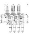
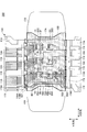
- FIG. 7 is a diagram showing a state in which IGBTs 20A to 20C and diodes 30A to 30C are connected to a lead frame 10 of a comparative example.
- FIG. It is a figure which shows the power module 60 of a comparative example. It is a figure which shows schematic structure of one Example of the drive device 300 for electric vehicles containing the power module 200 of embodiment.
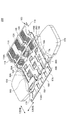
- 1 is a perspective perspective view showing a lead frame 100 and a power module 200 of an embodiment. It is a perspective view which shows the power module 200 of embodiment. It is a plane perspective view showing power module 200 including lead frame 100 of an embodiment.
- FIG. 5B is a perspective plan view showing the power module 200 in a state completed by cutting the guide frame 119 from the lead frame 100 shown in FIG. 5A.
- FIG. 5B It is a figure which shows the manufacturing process of the power module 200 of embodiment in steps. It is a figure which shows the manufacturing process of the power module 200 of embodiment in steps. It is a figure which shows the manufacturing process of the power module 200 of embodiment in steps. It is a figure which shows the manufacturing process of the power module 200 of embodiment in steps. It is a figure which shows the manufacturing process of the power module 200 of embodiment in steps. It is a figure which shows the manufacturing process of the power module 200 of embodiment in steps.
- FIG. 1 is a diagram showing a state in which IGBTs (Insulated Gate Bipolar Transistors) 20A to 20C and diodes 30A to 30C are connected to a lead frame 10 of a comparative example.
- IGBTs Insulated Gate Bipolar Transistors
- diodes 30A to 30C for example, FWD (Fly Wheel Diode) may be used.
- the lead frame 10 of the comparative example includes signal lead portions 11A, 12A, and 13A, power lead portions 14A, 15A, 16A, and 17A, and a voltage detection lead portion 18A.
- signal lead portions 11A, 12A, and 13A By removing the lead frame 10 later, except for the portions remaining as signal lead portions 11, 12, 13, power lead portions 14, 15, 16, 17, and voltage detection lead portion 18 (see FIG. 2), It functions as a guide frame 19.
- Such a lead frame 10 is manufactured, for example, by pressing a copper plate.
- the IGBTs 20A to 20C and the diodes 30A to 30C are soldered to the upper surface of the heat spreader 40.
- the lead frame 10 is covered from the upper side of the IGBTs 20A to 20C and the diodes 30A to 30C mounted on the heat spreader 40, and the lead frame 10 is connected to the IGBTs 20A to 20C and the diodes 30A to 30C with bonding wires and solder. State.
- IGBTs 20A to 20C are simply referred to as IGBT 20 unless otherwise distinguished.
- diodes 30A to 30C are not particularly distinguished, they are simply referred to as a diode 30.
- the heat spreader 40 is made of, for example, a copper plate, and is provided to dissipate heat from the IGBTs 20A to 20C and the diodes 30A to 30C.
- collector terminals on the lower surface in FIG. 1 are connected to heat spreader 40 by soldering, and in diodes 30A to 30C, cathodes on the lower surface in FIG. 1 are connected to heat spreader 40 by soldering.
- the power lead portion 14A is connected to the surface of the heat spreader 40 by solder 2A.
- the power lead portion 15A is connected to the emitter terminal of the IGBT 20A by the solder 2B, and is connected to the anode of the diode 30A by the solder 2C.
- the power lead portion 16A is connected to the emitter terminal of the IGBT 20B by the solder 2D, and is connected to the anode of the diode 30B by the solder 2E.
- the power lead portion 17A is connected to the emitter terminal of the IGBT 20C by solder 2F and is connected to the anode of the diode 30C by solder 2G.
- the voltage detection lead portion 18A is connected to the end portion of the surface of the heat spreader 40 by the bonding wire 3.
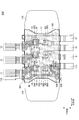
- FIG. 2 is a diagram showing a power module 60 of a comparative example.
- the power module 60 includes signal lead parts 11, 12, 13, power lead parts 14, 15, 16, 17, a voltage detection lead part 18, an IGBT 20, a diode 30, a heat spreader 40, and a mold resin part 50.
- the signal lead parts 11, 12, and 13, the power lead parts 14, 15, 16, and 17, and the voltage detection lead part 18 shown in FIG. 2 are respectively the signal lead parts 11A, 12A, and 13A, and the power lead part shown in FIG. 14A, 15A, 16A, 17A, and the voltage detection lead 18A.
- the signal lead portions 11, 12, and 13, the power lead portions 14, 15, 16, and 17, and the voltage detection lead portion 18 shown in FIG. 2 are obtained by cutting the guide frame 19 from the lead frame 10 shown in FIG. .
- the signal lead parts 11, 12, 13, the power lead parts 14, 15, 16, 17, the voltage detection lead part 18, the IGBT 20, the diode 30, and the heat spreader 40 are fixed by a mold resin part 50.
- the mold resin portion 50 is manufactured, for example, by performing molding while heating using a thermosetting epoxy resin.
- the lead frame 10 including the guide frame 19 is used for the signal lead portions 11, 12 and 13, the power lead portions 14, 15, 16 and 17, and the voltage detection lead portion. This is because the positioning accuracy of 18 is increased.
- Such a power module 60 can be used as an upper arm of an inverter, for example.
- a power module similar to the power module 60 may be used as the lower arm of the inverter.
- the power module used as the lower arm may be any module obtained by removing the voltage detection lead portion 18 from the power module 60, for example.
- the drive control of the three-phase motor is performed. It can be carried out.
- the voltage detection lead portion 18A shown in FIG. 1 is connected to the end of the surface of the heat spreader 40 by the bonding wire 3. Since the collector terminal of the IGBT 20 is soldered to the heat spreader 40, the heat spreader 40 has the same potential as the collector terminal of the IGBT 20.
- the voltage detection lead portion 18 obtained by cutting the guide frame 19 from the lead frame 10 is connected to the collector terminal of the IGBT 20 on the upper arm of the inverter.
- the collector terminal of the IGBT 20 on the upper arm of the inverter is at the same potential as the positive terminal of the inverter, the voltage of the positive terminal of the inverter can be detected through the voltage detection lead portion 18.
- the lead frame 10 used in the power module 60 of the comparative example includes many portions discarded as the guide frame 19 as can be understood by comparing FIG. 1 and FIG. For this reason, the lead frame 10 used in the power module 60 of the comparative example has a problem that the material yield is low.
- the linear expansion coefficient of the copper lead frame 10 is much larger than the linear expansion coefficient of the mold resin portion 50. Therefore, when the power module 60 is cooled after heating for molding and forming the mold resin part 50, the guide frame 19 contracts more than the mold resin part 50, thereby causing the signal lead part 11, 12 and 13, power lead portions 14, 15, 16 and 17, and voltage detection lead portion 18 are distorted.
- a thin cutting die is provided in the region B between the mold resin portion 50 (see FIG. 2) and the guide frame 19. insert.
- the width B1 of the region B is narrow, for example, when metal wear occurs in a thin mold, there is a problem that burrs may occur in the mold resin portion 50.
- the voltage detection lead portion 18 is connected to the surface of the heat spreader 40 by the bonding wire 3, a process for forming the bonding wire 3 is necessary, and the number of manufacturing steps increases, resulting in an increase in the cost of the power module 60. There was a problem.
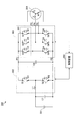
- FIG. 3 is a diagram showing a schematic configuration of an example of an electric vehicle drive device 300 including the power module 200 of the embodiment.
- the electric vehicle drive device 300 is a device that drives the vehicle by driving the travel motor 304 using the electric power of the battery 301.
- the details of the method and the configuration of the electric vehicle are arbitrary as long as the electric vehicle travels by driving the traveling motor 304 using electric power.
- the electric vehicle typically includes a hybrid vehicle (HV) whose power source is an engine and a traveling motor 304, and an electric vehicle whose power source is only the traveling motor 304.
- HV hybrid vehicle
- the electric vehicle drive device 300 includes a battery 301, a DC / DC converter 302, an inverter 303, a travel motor 304, and a control device 305.
- the battery 301 is an arbitrary power storage device that accumulates electric power and outputs a DC voltage, and may include a capacitive load such as a nickel metal hydride battery, a lithium ion battery, or an electric double layer capacitor.
- the DC / DC converter 302 is a bidirectional DC / DC converter (reversible chopper boost DC / DC converter), and can perform, for example, step-up conversion from 14V to 42V and step-down conversion from 42V to 14V.
- DC / DC converter 302 includes switching elements Q1, Q2, diodes D1, D2, and a reactor L1.
- the switching elements Q1 and Q2 are IGBTs (Insulated Gate Bipolar Transistors) in this example, but other switching elements such as MOSFETs (Metal Oxide Semiconductors Field-Effect Transistors) may be used.
- IGBTs Insulated Gate Bipolar Transistors
- MOSFETs Metal Oxide Semiconductors Field-Effect Transistors
- Switching elements Q1, Q2 are connected in series between the positive line and the negative line of inverter 303.
- the collector of the switching element Q1 in the upper arm is connected to the positive line
- the emitter of the switching element Q2 in the lower arm is connected to the negative line.
- One end of reactor L1 is connected to the intermediate point of switching elements Q1, Q2, that is, the connection point between the emitter of switching element Q1 and the collector of switching element Q2.
- the other end of the reactor L1 is connected to the positive electrode of the battery 301 via a positive electrode line.
- the emitter of the switching element Q2 is connected to the negative electrode of the battery 301 via the negative electrode line.
- diodes (flywheel diodes) D1 and D2 are arranged between the collectors and emitters of the switching elements Q1 and Q2 so that current flows from the emitter side to the collector side. Further, a smoothing capacitor C1 is connected between the other end of the reactor L1 and the negative electrode line, and a smoothing capacitor C2 is connected between the collector of the switching element Q1 and the negative electrode line.
- the inverter 303 includes U-phase, V-phase, and W-phase arms arranged in parallel between the positive electrode line and the negative electrode line.
- the U phase consists of a series connection of switching elements (IGBTs in this example) Q3, Q4, the V phase consists of a series connection of switching elements (IGBTs in this example) Q5, Q6, and the W phase is a switching element (in this example IGBTs).
- It consists of a series connection of Q7 and Q8.
- diodes (flywheel diodes) D3 to D8 are arranged between the collectors and emitters of the switching elements Q3 to Q8 so as to allow current to flow from the emitter side to the collector side, respectively.
- the upper arm of the inverter 303 is composed of switching elements Q3, Q5, Q7 and diodes D3, D5, D7.
- the lower arm of the inverter 303 is composed of switching elements Q4, Q6, Q8 and diodes D4, D6, D8. Consists of
- the inverter 303 is realized by including the power module 200 as an upper arm, for example.
- the lower arm of the inverter 303 any type of power module including switching elements Q4, Q6, Q8 and diodes D4, D6, D8 can be used.
- the traveling motor 304 is a three-phase permanent magnet motor, and one end of three U, V, and W coils is commonly connected at a midpoint.
- the other end of the U-phase coil is connected to an intermediate point between the switching elements Q3 and Q4, the other end of the V-phase coil is connected to an intermediate point between the switching elements Q5 and Q6, and the other end of the W-phase coil is connected to the switching element. Connected to the midpoint between Q7 and Q8.
- the control device 305 controls the DC / DC converter 302 and the inverter 303.
- the control device 305 includes, for example, a CPU, a ROM, a main memory, and the like, and various functions of the control device 305 are realized by a control program recorded in the ROM or the like being read into the main memory and executed by the CPU. .
- a part or all of the control device 305 may be realized only by hardware.
- the control device 305 may be physically configured by a plurality of devices.
- FIG. 4A is a perspective perspective view showing the lead frame 100 and the power module 200 of the embodiment.
- FIG. 4B is a perspective view illustrating the power module 200 according to the embodiment.
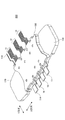
- FIG. 5A is a plan perspective view showing a power module 200 including the lead frame 100 of the embodiment.
- 5B is a plan perspective view showing the power module 200 in a state where the guide frame 119 is cut off from the lead frame 100 shown in FIG. 5A and completed.
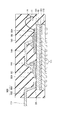
- FIG. 6 is a view showing a CC cross section in FIG. 5B.
- 4A and 5A show the lead frame 100 and the power module 200 in a state before the guide frame 119 of the lead frame 100 is cut off.
- 4B and 5B show the power module 200 in a completed state after the guide frame 119 of the lead frame 100 is cut away.
- the lead frame 100 and the power module 200 shown in FIGS. 4A, 4B, 5A, 5B, and 6 are the same as those of the lead frame 10 and the power module 60 of the comparative example shown in FIGS. Are denoted by the same reference numerals, and the description thereof is omitted.
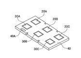
- the power module 200 includes a lead frame 100, IGBTs 20A to 20C, diodes 30A to 30C, a heat spreader 40, a mold resin portion 150, a cooling plate 170, and an insulating sheet 180 as main components.
- the IGBTs 20A to 20C and the diodes 30A to 30C of the power module 200 are soldered on the heat spreader 40 as in the power module 60 of the comparative example.
- the IGBT 20 ⁇ / b> A is connected to the surface of the heat spreader 40 by solder 191. Since there is a collector terminal on the lower surface connected to the heat spreader 40 by the solder 191, the collector terminal of the IGBT 20 ⁇ / b> A is connected to the heat spreader 40 by the solder 191.
- the diode 30A is connected to the heat spreader 40 by solder 192. Since there is a cathode on the lower surface of the diode 30A connected to the heat spreader 40 by the solder 192, the cathode of the diode 30A is connected to the heat spreader 40 by the solder 192.
- FIG. 6 shows a cross section including the IGBT 20A.
- the IGBTs 20B and 20C are connected to the heat spreader 40 by the solder 191 with the collector terminal positioned on the lower surface.
- the diodes 30B and 30C are connected to the heat spreader 40 by the solder 192 with the cathode facing down.
- the heat spreader 40 to which the IGBTs 20A to 20C and the diodes 30A to 30C are soldered is connected to the lead frame 100 and is placed on the cooling plate 170 through the insulating sheet 180 and is molded by transfer molding. It is sealed with a mold resin part 150.
- the lead frame 100 includes a voltage detection lead portion 118A, a guide frame 119, and wiring. Part 500 is included.
- the signal lead portions 11A, 12A, and 13A are examples of the first lead portion.
- the power lead portions 15A, 16A, and 17A are examples of the second lead portion.
- the voltage detection lead portion 118A is an example of a third lead portion.
- the wiring unit 500 is an example of a wiring unit connected to the third lead.
- the power lead portion 114A is an example of a fourth lead portion.
- the lead frame 100 is manufactured, for example, by pressing a copper plate.
- the voltage detection lead portion 118A corresponds to the voltage detection lead portion 18A in the lead frame 10 of the comparative example.
- the voltage detection lead portion 118A becomes the voltage detection lead portion 118 shown in FIGS. 4B and 5B.
- the voltage detection lead part 118A is arranged outside the signal lead part (the signal lead part arranged at the leftmost of the five signal lead parts 11A) located at the end of the signal lead parts 11A, 12A, 13A. Are arranged as follows.
- the wiring portion 500 is a portion indicated by hatching in FIGS. 5A and 5B, and has one end 501, the other end 502, and a connection portion 503.
- the one end 501 is connected to the voltage detection lead part 118A outside the mold resin part 150.
- the other end 502 is connected to the power lead part 114A.
- the connection part 503 is connected to the surface of the heat spreader 40 by the solder 2A.
- the wiring part 500 has one end 501 located outside the mold resin part 150, but the part other than the one end 501 is sealed by the mold resin part 150.
- the power lead portion 114 ⁇ / b> A is connected to the other end 502 of the wiring portion 500, and is a portion located outside the mold resin portion 150.
- the power lead portion 114A is located on the outermost side of the power lead portions 15, 16, and 17, and is located at the end of the signal lead portions 11A, 12A, and 13A (out of the five signal lead portions 11A).
- the signal lead portions 11, 12, and 13, the power lead portions 114, 15, 16, and 17, the voltage detection lead portion 118, and the wiring portion 500 shown in FIGS. 4B and 5B are the signal leads shown in FIGS. 4A and 5A, respectively. It is obtained by cutting the guide frame 119 from the lead frame 100 including the portions 11A, 12A, 13A, the power lead portions 114A, 15A, 16A, 17A, the voltage detection lead portion 118A, and the wiring portion 500.
- the guide frame 119 included in the lead frame 100 of the embodiment is a portion that disappears in FIG. 5B of the lead frame 100 shown in FIG. 5A.
- bonding wire 1A for example, an aluminum fine wire can be used as the bonding wire 1A, the bonding wire 1B, and the bonding wire 1C.
- an aluminum fine wire can be used as the bonding wire 1A, the bonding wire 1B, and the bonding wire 1C.
- connection part 503 of the wiring part 500 is connected to the surface of the heat spreader 40 by solder 2A.
- the connection portion 503 is connected to the voltage detection lead portion 118 (118A) via one end 501 and is connected to the power lead portion 114 (114A) via the other end 502.
- the power lead portion 15A is connected to the emitter terminal of the IGBT 20A by the solder 2B and is connected to the anode of the diode 30A by the solder 2C.
- the power lead portion 16A is connected to the emitter terminal of the IGBT 20B by solder 2D and is connected to the anode of the diode 30B by solder 2E.
- the power lead portion 17A is connected to the emitter terminal of the IGBT 20C by solder 2F and is connected to the anode of the diode 30C by solder 2G.
- the power lead portions 114 (114A), 15 (15A), 16 (16A), and 17 (17A) are configured to be wider than the signal lead portion 11 (11A).
- the collector terminal of the IGBT 20 ⁇ / b> A is connected to the heat spreader 40 by solder 191, and the cathode of the diode 30 ⁇ / b> A is connected by solder 192. Further, as described above, the connection part 503 of the wiring part 500 is connected to the heat spreader 40 by the solder 2A.
- the wiring part 500 is equipotential with the collector terminal of the IGBT 20A, and the potential of the collector terminal of the IGBT 20A can be detected via the wiring part 500 and the voltage detection lead part 118.
- the X direction and the Y direction are defined as shown in FIGS. 4A, 4B, 5A, and 5B.
- the X direction and the Y direction are directions orthogonal to each other in a plane including the wiring part 500.
- the wiring part 500 is located on the outermost side in the X direction of the lead frame 100 as shown in FIGS. 4A and 5A.
- the wiring part 500 has one end 501 connected to the voltage detection lead part 118A, a part 119A and a part 119B of the guide frame in the Y direction.
- the other end 502 is connected to the connection portion 503, the power lead portion 14A, and a part 119C.
- the wiring unit 500 includes the voltage detection lead unit 118A, a part 119A and a part 119B of the guide frame, the connection unit 503, the power lead unit 14A, In addition, a guide frame is formed between the 119C and the part 119C.
- the wiring part 500 functions as a guide frame included in the lead frame 100, the voltage detection lead part 118A, part 119A and part 119B of the guide frame, the connection part 503, the power lead part 14A,
- the length, width, thickness, shape, and the like may be set so that the portion 119C has sufficient strength so as not to be bent or deformed.
- the wiring portion 500 of the lead frame 100 of the embodiment functions as a guide frame in a state before the guide frame 119 is cut, and the guide frame 119 is cut off. In the later state, as shown in FIGS. 4B and 5B, it functions as a wiring.
- the IGBT 20A and the diode 30A are connected to the U phase
- the IGBT 20B and the diode 30B are connected to the V phase
- the IGBT 20C and the diode 30C are connected to the W phase.
- the power lead portion 114 connected to the collectors of the IGBTs 20A to 20C and the cathodes of the diodes 30A to 30C via the connection portion 503 is connected to the positive terminal (in FIG. 3) of the inverter 303 (see FIG. Input terminal) P1.
- the voltage detection lead unit 118 connected to the power lead unit 114 via the wiring unit 500 can detect the input voltage of the inverter 103 (voltage of the positive terminal (input terminal) P1).
- the power lead 15 connected to the emitter of the IGBT 20A and the anode of the diode 30A constitutes the U-phase terminal P3 of the inverter 303 (see FIG. 3).
- the power lead 16 connected to the emitter of the IGBT 20B and the anode of the diode 30B constitutes the V-phase terminal P4 of the inverter 303 (see FIG. 3).
- the power lead portion 17 connected to the emitter of the IGBT 20C and the anode of the diode 30C constitutes the W-phase terminal P5 of the inverter 303 (see FIG. 3).
- the voltage detection lead 18 is removed from the power module 60 of the comparative example, and the lead connected to the emitter terminals of the switching elements Q4, Q6, Q8 in FIG. A power module to which is added may be used.
- the lead connected to the emitter terminals of the emitter terminals of the switching elements Q4, Q6, Q8 constitutes the negative terminal (input terminal) P2 of the inverter 303 (see FIG. 3). Further, the collector terminals of the switching elements Q4, Q6, and Q8 of the lower-arm power module may be connected to the U-phase terminal P3, the V-phase terminal P4, and the W-phase terminal P5, respectively.
- the cooling plate 170 is made of a material having good thermal conductivity, and may be made of a metal such as aluminum, for example.
- the cooling plate 170 has fins 171 on the lower surface side.
- the number and arrangement of the fins 171 are arbitrary unless otherwise specified. Further, the configuration (shape, height, etc.) of the fin 171 may be arbitrary.
- the fins 171 may be realized by, for example, a staggered arrangement of straight fins or pin fins. In the mounted state of the semiconductor module 1, the fins 171 are in contact with a cooling medium such as cooling water or cooling air.
- the fins 171 may be formed integrally with the cooling plate 170 (for example, aluminum die casting), or may be integrated with the cooling plate 170 by welding or the like.
- the cooling plate 170 may be configured by connecting one metal plate and another metal plate with fins with bolts or the like.
- the insulating sheet 180 is made of, for example, a resin sheet, and enables high heat conduction from the heat spreader 40 to the cooling plate 170 while ensuring electrical insulation between the heat spreader 40 and the cooling plate 170.
- the insulating sheet 180 has an outer shape larger than the lower surface of the heat spreader 40.
- the insulating sheet 180 preferably directly joins the heat spreader 40 and the cooling plate 170 without using solder or a metal film. Thereby, compared with the case where solder is used, thermal resistance can be made low and a process can be simplified. Further, the surface treatment for soldering is not necessary on the cooling plate 170 side.
- the insulating sheet 180 is made of a resin material (epoxy resin) similar to the mold resin portion 150 described later, and is joined to the heat spreader 40 and the cooling plate 170 by the pressure and temperature when the mold resin portion 150 is molded.
- the mold resin portion 150 excludes the ends of the wiring members of the IGBT 20 and the diode 30, the signal lead portions 11, 12, and 13 and the power lead portions 15, 16, and 17. It is formed by molding the portion, the portion excluding the end portion of the voltage detection lead portion 118, the wiring portion 500, the heat spreader 40, the cooling plate 170, and the insulating sheet 180 with resin.
- the mold resin portion 150 is connected to the upper surface of the cooling plate 170 with respect to the main components of the power module 200 (IGBT 20 and diode 30, signal lead portions 11, 12, 13 and power lead portions 15, 16, 17 wiring members. This is a portion that seals the portion excluding the end portion of this, the portion excluding the end portion of the voltage detection lead portion 118, the wiring portion 500, the heat spreader 40, and the insulating sheet 180).
- the resin used as the mold resin portion 150 may be an epoxy resin, for example.
- the end portions of the wiring members of the signal lead portions 11, 12, 13 and the power lead portions 15, 16, 17, the end portion of the voltage detection lead portion 118 A, and the power lead portion 114 are exposed from the mold resin portion 150.
- the ends of the wiring members of the signal leads 11, 12, and 13 and the power leads 15, 16, and 17, the end of the voltage detection lead 118A, and the power lead 114 are formed after the mold sealing by the mold resin portion 150.
- the final shape is realized by lead cutting and forming.
- FIG. 7 to 11 are diagrams showing the manufacturing process of the power module 200 of the embodiment step by step.
- the IGBTs 20A to 20C and the diodes 30A to 30C are mounted on the heat spreader 40 by soldering.
- the collector terminals of the IGBTs 20A to 20C are connected to the heat spreader 40 by solder 191 and the cathodes of the diodes 30A to 30C are connected to the heat spreader 40 by solder 192 (see FIG. 6).
- connection part 40A shown on the surface of the heat spreader 40 represents a position where the connection part 503 of the lead frame 100 is connected later.
- the lead frame 100 is placed on the IGBTs 20A to 20C and the diodes 30A to 30C mounted on the heat spreader 40 for alignment, and the IGBTs 20A to 20C and the diodes 30A to 30C are aligned. 30C and the lead frame 100 are connected by solder 2B to 2G.
- the signal leads 11A, 12A, 13A and the gate terminals of the IGBTs 20A, 20B, 20C are connected by bonding wires 1A, 1B, 1C.
- an insulating sheet 180 is bonded to a predetermined position on the cooling plate 170.
- the insulating sheet 180 is temporarily bonded to the surface of the heat spreader 40 by heating, for example.
- the IGBTs 20A to 20C and the diodes 30A to 30C and the lead frame 100 are formed on the insulating sheet 180 bonded to a predetermined position on the cooling plate 170 as shown in FIG.
- the heat spreader 40 that has been soldered is placed, and the mold resin portion 150 is formed by transfer molding.
- FIG. 10 transparently shows the mold resin portion 150 as in FIG. 4A.
- the end portions of the wiring members of the signal lead portions 11, 12, 13 and the power lead portions 15, 16, 17, the end portion of the voltage detection lead portion 118 ⁇ / b> A, and the power lead portion 114 are exposed from the mold resin portion 150. To do.
- the guide frame 119 functions as a guide frame in a state before the guide frame 119 is excised, and in the state after the guide frame 119 is excised, as shown in FIG. 4B and FIG.
- the lead frame 100 including the wiring part 500 that functions can be provided.
- the guide frame 19 (see FIGS. 1 and 2) was all discarded after being excised, and the material yield was low.
- the wiring portion 500 functions as a guide frame in a state before the guide frame 119 is cut, and in a state after the guide frame 119 is cut, As shown in FIGS. 4B and 5B, it functions as a wiring.
- the lead frame 100 of the present embodiment is used as the wiring unit 500 without cutting away a part of the guide frame.
- the lead frame 100 of the present embodiment has a wiring portion 500 with a mold resin. It is accommodated in the part 150.
- the lead frame 100 of the present embodiment can reduce the size of the wiring portion 500 and the structure around the wiring portion 500 in a plan view as compared with the lead frame 10 of the comparative example.
- the lead frame 100 of the present embodiment can be manufactured with fewer metal materials than the lead frame 10 of the comparative example.
- the lead frame 100 with improved material yield can be provided according to the present embodiment.
- the lead frame 100 of the present embodiment can be manufactured with a smaller amount of metal material, a larger number of lead frames 100 can be formed from the same amount of metal material than the lead frame 10 of the comparative example. Can be manufactured.
- the mold for cutting the guide frame 119 can be made smaller.
- the wiring part 500 of the lead frame 100 of the present embodiment has one end 501 connected to the voltage detection lead part 118, and the upper arm of the inverter 303 (see FIG. 3) via the heat spreader 40 by the solder 2A at the connection part 503. Is connected to the collector terminal of the IGBT 20A.
- the voltage detection lead 118 can be used as a terminal for monitoring the input voltage of the inverter 303 (the voltage of the positive terminal (input terminal) P1) simply by connecting the connection 503 to the heat spreader 40 with the solder 2A. it can.
- the manufacturing process can be reduced, and the cost of the power module 200 can be reduced. be able to.
- the lead frame 100 of the present embodiment can cut the guide frame 119 in a state where the wiring part 500 that functions as a part of the guide frame is sealed by the mold resin part 150.
- the wiring portion 500 that functions as a part of the guide frame of the lead frame 100 is fixed by the mold resin portion 150, so that distortion and warpage do not occur. Therefore, highly accurate lead cutting can be performed.
- this can suppress distortion and warpage in the end portions of the wiring members of the signal lead portions 11, 12, 13 and the power lead portions 15, 16, 17, the end portion of the voltage detection lead portion 118 ⁇ / b> A, and the power lead portion 114. .
- the reliability of the joints of the solders 2A to 2G can be improved, and the life of the joints of the solders 2A to 2G can be extended.
- the power module 200 may include other configurations (for example, a part of the elements of the DC / DC boost converter for driving the driving motor).
- the power module 200 may include other elements (capacitors, reactors, etc.) in addition to the semiconductor elements.
- the power module 200 is not limited to the semiconductor module which comprises an inverter.
- the power module 200 is not limited to an inverter for a vehicle, and may be realized as an inverter used for other purposes (railway, air conditioner, elevator, refrigerator, etc.).
Landscapes
- Inverter Devices (AREA)
- Lead Frames For Integrated Circuits (AREA)
- Engineering & Computer Science (AREA)
- Automation & Control Theory (AREA)
- Manufacturing & Machinery (AREA)
- Cooling Or The Like Of Semiconductors Or Solid State Devices (AREA)
- Microelectronics & Electronic Packaging (AREA)
Priority Applications (4)
| Application Number | Priority Date | Filing Date | Title |
|---|---|---|---|
| CN201280032343.5A CN103620768A (zh) | 2011-06-28 | 2012-04-26 | 引线框架及功率组件 |
| DE112012002724.8T DE112012002724T5 (de) | 2011-06-28 | 2012-04-26 | Leiterrahmen und Leistungsmodul |
| US14/129,342 US20140145193A1 (en) | 2011-06-28 | 2012-04-26 | Lead frame and power module |
| US15/195,466 US20160307829A1 (en) | 2011-06-28 | 2016-06-28 | Lead frame and power module |
Applications Claiming Priority (2)
| Application Number | Priority Date | Filing Date | Title |
|---|---|---|---|
| JP2011-143033 | 2011-06-28 | ||
| JP2011143033A JP5793995B2 (ja) | 2011-06-28 | 2011-06-28 | リードフレーム、及び、パワーモジュール |
Related Child Applications (2)
| Application Number | Title | Priority Date | Filing Date |
|---|---|---|---|
| US14/129,342 A-371-Of-International US20140145193A1 (en) | 2011-06-28 | 2012-04-26 | Lead frame and power module |
| US15/195,466 Division US20160307829A1 (en) | 2011-06-28 | 2016-06-28 | Lead frame and power module |
Publications (1)
| Publication Number | Publication Date |
|---|---|
| WO2013001905A1 true WO2013001905A1 (ja) | 2013-01-03 |
Family
ID=47423811
Family Applications (1)
| Application Number | Title | Priority Date | Filing Date |
|---|---|---|---|
| PCT/JP2012/061272 Ceased WO2013001905A1 (ja) | 2011-06-28 | 2012-04-26 | リードフレーム、及び、パワーモジュール |
Country Status (5)
| Country | Link |
|---|---|
| US (2) | US20140145193A1 (https=) |
| JP (1) | JP5793995B2 (https=) |
| CN (1) | CN103620768A (https=) |
| DE (1) | DE112012002724T5 (https=) |
| WO (1) | WO2013001905A1 (https=) |
Cited By (1)
| Publication number | Priority date | Publication date | Assignee | Title |
|---|---|---|---|---|
| CN105706233A (zh) * | 2013-11-05 | 2016-06-22 | 三菱电机株式会社 | 半导体模块 |
Families Citing this family (10)
| Publication number | Priority date | Publication date | Assignee | Title |
|---|---|---|---|---|
| JP6001473B2 (ja) * | 2013-02-12 | 2016-10-05 | トヨタ自動車株式会社 | 半導体装置の製造方法 |
| JP6001472B2 (ja) * | 2013-02-12 | 2016-10-05 | トヨタ自動車株式会社 | 半導体装置の製造方法 |
| JP6114134B2 (ja) * | 2013-07-29 | 2017-04-12 | トヨタ自動車株式会社 | リードフレーム、電力変換装置、半導体装置及び半導体装置の製造方法 |
| US10361147B1 (en) | 2018-06-28 | 2019-07-23 | Ford Global Technologies, Llc | Inverter power module lead frame with enhanced common source inductance |
| US11502045B2 (en) * | 2019-01-23 | 2022-11-15 | Texas Instruments Incorporated | Electronic device with step cut lead |
| JP7479759B2 (ja) | 2020-06-02 | 2024-05-09 | 三菱電機株式会社 | 半導体装置の製造方法、および、半導体装置 |
| JP7589560B2 (ja) * | 2021-01-15 | 2024-11-26 | 株式会社デンソー | 電気機器と電気機器の製造方法 |
| CN116686086A (zh) * | 2021-02-03 | 2023-09-01 | 罗姆股份有限公司 | 半导体装置 |
| JP7292352B2 (ja) | 2021-11-02 | 2023-06-16 | 三菱電機株式会社 | 樹脂封止型半導体装置及び樹脂封止型半導体装置の製造方法 |
| JP7715022B2 (ja) * | 2021-11-25 | 2025-07-30 | 三菱電機株式会社 | 半導体装置及び電力変換装置 |
Citations (2)
| Publication number | Priority date | Publication date | Assignee | Title |
|---|---|---|---|---|
| JPH03280562A (ja) * | 1990-03-29 | 1991-12-11 | Hitachi Ltd | リードフレーム及び半導体装置樹脂封止方法 |
| JP2001284518A (ja) * | 2000-02-29 | 2001-10-12 | Texas Instruments Tucson Corp | 低い温度係数のリードフレーム |
Family Cites Families (5)
| Publication number | Priority date | Publication date | Assignee | Title |
|---|---|---|---|---|
| JP4837236B2 (ja) * | 2001-04-04 | 2011-12-14 | 三菱電機株式会社 | 半導体装置 |
| US7884454B2 (en) * | 2005-01-05 | 2011-02-08 | Alpha & Omega Semiconductor, Ltd | Use of discrete conductive layer in semiconductor device to re-route bonding wires for semiconductor device package |
| US20060276157A1 (en) * | 2005-06-03 | 2006-12-07 | Chen Zhi N | Apparatus and methods for packaging antennas with integrated circuit chips for millimeter wave applications |
| JP5232367B2 (ja) * | 2006-07-12 | 2013-07-10 | ルネサスエレクトロニクス株式会社 | 半導体装置 |
| DE102007020618B8 (de) * | 2007-04-30 | 2009-03-12 | Danfoss Silicon Power Gmbh | Verfahren zum Herstellen eines festen Leistungsmoduls und damit hergestelltes Transistormodul |
-
2011
- 2011-06-28 JP JP2011143033A patent/JP5793995B2/ja not_active Expired - Fee Related
-
2012
- 2012-04-26 CN CN201280032343.5A patent/CN103620768A/zh active Pending
- 2012-04-26 US US14/129,342 patent/US20140145193A1/en not_active Abandoned
- 2012-04-26 DE DE112012002724.8T patent/DE112012002724T5/de not_active Withdrawn
- 2012-04-26 WO PCT/JP2012/061272 patent/WO2013001905A1/ja not_active Ceased
-
2016
- 2016-06-28 US US15/195,466 patent/US20160307829A1/en not_active Abandoned
Patent Citations (2)
| Publication number | Priority date | Publication date | Assignee | Title |
|---|---|---|---|---|
| JPH03280562A (ja) * | 1990-03-29 | 1991-12-11 | Hitachi Ltd | リードフレーム及び半導体装置樹脂封止方法 |
| JP2001284518A (ja) * | 2000-02-29 | 2001-10-12 | Texas Instruments Tucson Corp | 低い温度係数のリードフレーム |
Cited By (2)
| Publication number | Priority date | Publication date | Assignee | Title |
|---|---|---|---|---|
| CN105706233A (zh) * | 2013-11-05 | 2016-06-22 | 三菱电机株式会社 | 半导体模块 |
| CN105706233B (zh) * | 2013-11-05 | 2018-11-09 | 三菱电机株式会社 | 半导体模块 |
Also Published As
| Publication number | Publication date |
|---|---|
| JP5793995B2 (ja) | 2015-10-14 |
| US20140145193A1 (en) | 2014-05-29 |
| DE112012002724T5 (de) | 2014-03-13 |
| CN103620768A (zh) | 2014-03-05 |
| JP2013012525A (ja) | 2013-01-17 |
| US20160307829A1 (en) | 2016-10-20 |
Similar Documents
| Publication | Publication Date | Title |
|---|---|---|
| JP5793995B2 (ja) | リードフレーム、及び、パワーモジュール | |
| JP5846123B2 (ja) | パワーモジュール | |
| CN103348468B (zh) | 半导体组件及半导体组件的制造方法 | |
| JP5506740B2 (ja) | 電力変換装置 | |
| JP5427745B2 (ja) | パワー半導体モジュール及びその製造方法 | |
| JP6208262B2 (ja) | パワー半導体装置の製造方法、パワー半導体装置並びにそれを用いた電力変換装置 | |
| US20140035112A1 (en) | Semiconductor device and manufacturing method thereof | |
| CN110178304B (zh) | 半导体装置 | |
| US10279653B2 (en) | Power converter | |
| CN108133927B (zh) | 半导体装置及电力变换装置 | |
| JP7074046B2 (ja) | 半導体装置とその製造方法 | |
| US20240079383A1 (en) | Semiconductor device | |
| JP6401444B2 (ja) | パワーモジュールおよびその製造方法 | |
| JP5948106B2 (ja) | パワー半導体モジュール及びそれを用いた電力変換装置 | |
| CN113614917B (zh) | 功率半导体装置 | |
| JP7535909B2 (ja) | 電力用半導体装置およびその製造方法ならびに電力変換装置 | |
| US20250343105A1 (en) | Power conversion device | |
| WO2023100980A1 (ja) | 半導体モジュール、電力変換装置および電力変換装置の製造方法 | |
| WO2025197363A1 (ja) | 半導体装置およびその製造方法 | |
| WO2025253910A1 (ja) | パワーモジュールおよび電力変換装置 | |
| JP2026002560A (ja) | 半導体モジュールおよび電力変換装置 |
Legal Events
| Date | Code | Title | Description |
|---|---|---|---|
| 121 | Ep: the epo has been informed by wipo that ep was designated in this application |
Ref document number: 12805243 Country of ref document: EP Kind code of ref document: A1 |
|
| WWE | Wipo information: entry into national phase |
Ref document number: 14129342 Country of ref document: US |
|
| WWE | Wipo information: entry into national phase |
Ref document number: 1120120027248 Country of ref document: DE Ref document number: 112012002724 Country of ref document: DE |
|
| 122 | Ep: pct application non-entry in european phase |
Ref document number: 12805243 Country of ref document: EP Kind code of ref document: A1 |