WO2012176516A1 - 太陽電池モジュール - Google Patents
太陽電池モジュール Download PDFInfo
- Publication number
- WO2012176516A1 WO2012176516A1 PCT/JP2012/056857 JP2012056857W WO2012176516A1 WO 2012176516 A1 WO2012176516 A1 WO 2012176516A1 JP 2012056857 W JP2012056857 W JP 2012056857W WO 2012176516 A1 WO2012176516 A1 WO 2012176516A1
- Authority
- WO
- WIPO (PCT)
- Prior art keywords
- solar cell
- bus bar
- bar portion
- light
- light reflecting
- Prior art date
- Legal status (The legal status is an assumption and is not a legal conclusion. Google has not performed a legal analysis and makes no representation as to the accuracy of the status listed.)
- Ceased
Links
Images


Classifications
-
- H—ELECTRICITY
- H10—SEMICONDUCTOR DEVICES; ELECTRIC SOLID-STATE DEVICES NOT OTHERWISE PROVIDED FOR
- H10F—INORGANIC SEMICONDUCTOR DEVICES SENSITIVE TO INFRARED RADIATION, LIGHT, ELECTROMAGNETIC RADIATION OF SHORTER WAVELENGTH OR CORPUSCULAR RADIATION
- H10F77/00—Constructional details of devices covered by this subclass
- H10F77/60—Arrangements for cooling, heating, ventilating or compensating for temperature fluctuations
- H10F77/63—Arrangements for cooling directly associated or integrated with photovoltaic cells, e.g. heat sinks directly associated with the photovoltaic cells or integrated Peltier elements for active cooling
- H10F77/67—Arrangements for cooling directly associated or integrated with photovoltaic cells, e.g. heat sinks directly associated with the photovoltaic cells or integrated Peltier elements for active cooling including means to utilise heat energy directly associated with the photovoltaic cells, e.g. integrated Seebeck elements
-
- H—ELECTRICITY
- H10—SEMICONDUCTOR DEVICES; ELECTRIC SOLID-STATE DEVICES NOT OTHERWISE PROVIDED FOR
- H10F—INORGANIC SEMICONDUCTOR DEVICES SENSITIVE TO INFRARED RADIATION, LIGHT, ELECTROMAGNETIC RADIATION OF SHORTER WAVELENGTH OR CORPUSCULAR RADIATION
- H10F19/00—Integrated devices, or assemblies of multiple devices, comprising at least one photovoltaic cell covered by group H10F10/00, e.g. photovoltaic modules
- H10F19/80—Encapsulations or containers for integrated devices, or assemblies of multiple devices, having photovoltaic cells
-
- H—ELECTRICITY
- H10—SEMICONDUCTOR DEVICES; ELECTRIC SOLID-STATE DEVICES NOT OTHERWISE PROVIDED FOR
- H10F—INORGANIC SEMICONDUCTOR DEVICES SENSITIVE TO INFRARED RADIATION, LIGHT, ELECTROMAGNETIC RADIATION OF SHORTER WAVELENGTH OR CORPUSCULAR RADIATION
- H10F19/00—Integrated devices, or assemblies of multiple devices, comprising at least one photovoltaic cell covered by group H10F10/00, e.g. photovoltaic modules
- H10F19/90—Structures for connecting between photovoltaic cells, e.g. interconnections or insulating spacers
- H10F19/902—Structures for connecting between photovoltaic cells, e.g. interconnections or insulating spacers for series or parallel connection of photovoltaic cells
- H10F19/904—Structures for connecting between photovoltaic cells, e.g. interconnections or insulating spacers for series or parallel connection of photovoltaic cells characterised by the shapes of the structures
-
- H—ELECTRICITY
- H10—SEMICONDUCTOR DEVICES; ELECTRIC SOLID-STATE DEVICES NOT OTHERWISE PROVIDED FOR
- H10F—INORGANIC SEMICONDUCTOR DEVICES SENSITIVE TO INFRARED RADIATION, LIGHT, ELECTROMAGNETIC RADIATION OF SHORTER WAVELENGTH OR CORPUSCULAR RADIATION
- H10F77/00—Constructional details of devices covered by this subclass
- H10F77/40—Optical elements or arrangements
- H10F77/42—Optical elements or arrangements directly associated or integrated with photovoltaic cells, e.g. light-reflecting means or light-concentrating means
- H10F77/488—Reflecting light-concentrating means, e.g. parabolic mirrors or concentrators using total internal reflection
-
- Y—GENERAL TAGGING OF NEW TECHNOLOGICAL DEVELOPMENTS; GENERAL TAGGING OF CROSS-SECTIONAL TECHNOLOGIES SPANNING OVER SEVERAL SECTIONS OF THE IPC; TECHNICAL SUBJECTS COVERED BY FORMER USPC CROSS-REFERENCE ART COLLECTIONS [XRACs] AND DIGESTS
- Y02—TECHNOLOGIES OR APPLICATIONS FOR MITIGATION OR ADAPTATION AGAINST CLIMATE CHANGE
- Y02E—REDUCTION OF GREENHOUSE GAS [GHG] EMISSIONS, RELATED TO ENERGY GENERATION, TRANSMISSION OR DISTRIBUTION
- Y02E10/00—Energy generation through renewable energy sources
- Y02E10/50—Photovoltaic [PV] energy
- Y02E10/52—PV systems with concentrators
Definitions
- the present invention relates to a solar cell module having a plurality of solar cells.
- a solar cell module including a plurality of back junction solar cells is known (see, for example, Patent Document 1).
- a back junction solar cell it is not always necessary to provide an electrode on the light receiving surface. Therefore, according to the solar cell module including the back junction solar cell, improved output characteristics can be realized.
- An object of the present invention is to provide a solar cell module having improved output characteristics.
- the solar cell module according to the present invention includes a plurality of solar cells and a translucent first protective member.
- the solar cell has a first electrode that collects minority carriers and a second electrode that collects majority carriers on the back surface side.
- the 1st protection member is distribute
- the first electrode has a first bus bar portion arranged along one side and a plurality of first finger portions electrically connected to the first bus bar portion.
- the second electrode has a second bus bar portion arranged along the other side facing one side, and a plurality of second finger portions electrically connected to the second bus bar portion.
- the first bus bar portion of one solar cell of the solar cells adjacent to each other faces the second bus bar portion of the other solar cell.
- the solar cell module according to the present invention further includes a light reflecting surface arranged in a region between one solar cell and the other solar cell. The light reflecting surface reflects more light incident on the region from the first protective member side to the one solar cell side than the
- a solar cell module having improved output characteristics can be provided.
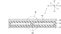
- FIG. 1 is a schematic cross-sectional view of the solar cell module according to the first embodiment.
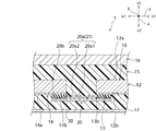
- FIG. 2 is a schematic cross-sectional view enlarging the II portion of FIG.
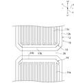
- FIG. 3 is a partial schematic plan view of a plurality of solar cells included in the solar cell module according to the first embodiment.
- FIG. 4 is an explanatory diagram for explaining the effect of the solar cell module according to the first embodiment.
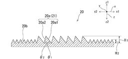
- FIG. 5 is a schematic cross-sectional view of the wiring member according to the first embodiment.
- FIG. 6 is a schematic cross-sectional view of the wiring member according to the second embodiment.
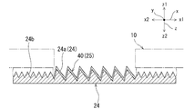
- FIG. 7 is a schematic cross-sectional view for explaining a light reflecting surface in the third embodiment.
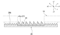
- FIG. 8 is a schematic cross-sectional view for explaining a light reflecting surface in the fourth embodiment.
- the solar cell module 1 As shown in FIG. 1, the solar cell module 1 according to this embodiment includes a first protection member 16, a second protection member 17, and between the first protection member 16 and the second protection member 17. Thus, a plurality of solar cells 10 sealed in the sealing material 15 are provided.
- the first protective member 16 has translucency and protects the light receiving surface side of the solar cell 10.
- the first protective member 16 can be formed of a translucent plate such as a glass plate or a translucent plastic plate. Of the light incident on the solar cell module 1, at least part of the light transmitted through the first protective member 16 is incident on the light receiving surface of the solar cell 10.
- the second protective member 17 protects the back side of the solar cell 10.
- the second protective member 17 can be composed of a weather resistant member such as a weather resistant resin film or a laminated film formed by sandwiching a metal foil between a pair of resin films.
- the sealing material 15 can be made of a resin material such as ethylene / vinyl acetate copolymer (EVA), polyvinyl butyral (PVB), polyethylene (PE), polyurethane (PU), or the like.
- EVA ethylene / vinyl acetate copolymer
- PVB polyvinyl butyral
- PE polyethylene
- PU polyurethane
- the solar cell module 1 may have a terminal box on the surface of the second protective member 17 for taking out the generated power of the plurality of solar cells 10 to the outside. Moreover, you may have a metal-made or resin-made frame in the peripheral part.
- the solar cell 10 is a back junction solar cell.
- the solar cell 10 includes a photoelectric conversion unit 12 (see FIGS. 2 and 3).
- the photoelectric conversion unit 12 has a light receiving surface 12a and a back surface 12b, and has electrodes on the back surface 12b. The configuration of the electrode will be described later.
- the light receiving surface 12a is a surface that mainly receives light and is disposed on the first protection member 16 side.
- the photoelectric conversion unit 12 generates carriers by receiving light on the light receiving surface 12a.
- the solar cell 10 may have a passivation layer or an antireflection layer on the light receiving surface 12a.
- the photoelectric conversion unit 12 is not particularly limited as long as it has a p-type surface and an n-type surface (not shown) on the back surface 12b.
- the photoelectric conversion unit 12 may include a substrate made of a semiconductor material having one conductivity type, and a p-type semiconductor layer and an n-type semiconductor layer disposed on the back surface of the substrate. In that case, a substantially intrinsic i-type semiconductor layer having a thickness that does not substantially contribute to power generation may be disposed between the p-type semiconductor layer and the n-type semiconductor layer and the substrate. Further, the photoelectric conversion unit 12 may have a p-type dopant diffusion region and an n-type dopant diffusion region on the back surface of the substrate made of a semiconductor material.
- the first electrode 13 and the second electrode 14 are arranged on the back surface 12b of the photoelectric conversion unit 12.
- One of the first electrode 13 and the second electrode 14 is disposed on the p-type surface, and the other is disposed on the n-type surface.
- the first electrode 13 is an electrode that collects minority carriers
- the second electrode 14 is an electrode that collects majority carriers.
- the photoelectric conversion unit 12 includes a substrate made of an n-type semiconductor material
- the first electrode 13 is a p-side electrode
- the second electrode 14 is an n-side electrode.
- the first electrode 13 has a plurality of first finger portions 13a and a first bus bar portion 13b.
- the first bus bar portion 13b extends in the y direction (first direction) along one side of the photoelectric conversion portion 12 having a substantially rectangular shape. As shown in FIG. 3, the shape of the photoelectric conversion unit 12 may be a substantially square shape, and may be a substantially rectangular shape with four corners cut.
- Each of the plurality of first finger portions 13a extends in a line along the x direction (second direction) intersecting with the y direction, and is arranged at intervals from each other along the y direction.
- the first bus bar portion 13b is electrically connected to the plurality of first finger portions 13a.
- the first bus bar portions 13b collect minority carriers collected by the respective first finger portions 13a. For this reason, the width
- the second electrode 14 has a plurality of second finger portions 14a and a second bus bar portion 14b.
- the second bus bar portion 14b extends in the y direction so as to extend along the other side of the photoelectric conversion unit 12 that faces the one side along which the first bus bar portion 13b described above extends.
- Each of the plurality of second finger portions 14a extends in a line shape along the x direction, and is arranged at an interval along the y direction.
- the plurality of first finger portions 13a and the plurality of second finger portions 14a are alternately arranged at intervals along the y direction.
- the second bus bar portion 14b is electrically connected to the plurality of second finger portions 14a.
- the second bus bar portions 14b collect the majority carriers collected by the respective second finger portions 14a. For this reason, the width
- the plurality of solar cells 10 are electrically connected by the wiring material 20.
- the wiring member 20 is arranged between the solar cells 10 adjacent in the x direction. Adjacent solar cells 10 are arranged such that the first bus bar portion 13b of one solar cell 10 and the second bus bar portion 14b of the other solar cell face each other.
- the wiring member 20 electrically connects the first bus bar portion 13 b of one solar cell 10 and the second bus bar portion 14 b of the other solar cell 10.
- the solar cell module 1 further includes a light reflecting surface 21 facing the first protection member 16 in a region between the solar cells 10 connected by the wiring member 20.
- the light reflecting surface 21 is constituted by the surface of the wiring member 20.
- the wiring member 20 has a first uneven surface 20a on the surface of the first protective member 16 side.
- the first concavo-convex surface 20 a is provided including the central portion between the solar cells 10 connected by the wiring member 20.
- the light reflecting surface 21 is constituted by the first uneven surface 20a.
- the “concave / convex surface” is a general term for a surface composed of only a convex surface, a surface composed of only a concave surface, and a surface composed of a convex surface and a concave surface.
- the light reflecting surface 21 configured by the first uneven surface 20 a transmits the light L that has passed through the first protective member 16 and is incident between the adjacent solar cells 10 to one of the suns.
- the light is mainly reflected on the battery 10 side (the solar cell 10 side located on the x1 side in the x direction of the light reflecting surface 21). That is, of the light reflected by the light reflecting surface 21, the amount of light reflected on the side of the solar cell 10 located on the other side (x2 side of the light reflecting surface 21) is reflected on the one solar cell 10 side.
- a light reflecting surface 21 is provided between adjacent solar cells 10 so that the amount of light to be increased.
- the first uneven surface 20a constituting the light reflecting surface 21 includes a first slope portion 20a1 whose normal is directed to one solar cell 10 side, 2nd slope part 20a2 in which a line
- the first uneven surface 20a is configured such that the area occupied by the first inclined surface portion 20a1 is larger than the area occupied by the second inclined surface portion 20a2 in a plan view (when viewed from the z direction). . That is, the base angle ⁇ 1 of the first slope portion 20a1 is smaller than the base angle ⁇ 2 of the second slope portion 20a2 ( ⁇ 2 > ⁇ 1 ).
- each of the first inclined surface portion 20 a 1 and the second inclined surface portion 20 a 2 is such that most of the light reflected by the light reflecting surface 21 toward the one solar cell 10 is blocked by the solar cell 10. It sets suitably so that it may reach the 1st protection member 16 without being done.
- the wiring material 20 has the 2nd uneven surface 20b with the above-mentioned 1st uneven surface 20a on the surface by the side of the solar cell 10.
- FIG. The second uneven surface 20 b is disposed to face the back surface of the solar cell 10.
- the second uneven surface 20 b is bonded to the solar cell 10 by the adhesive layer 30.
- region of the solar cell 10 and the wiring material 20 is formed in the 2nd uneven surface 20b, it may be flat instead of an uneven surface.
- the 2nd uneven surface 20b and the 1st uneven surface 20a may have the same shape, and may have a mutually different shape.
- the two inclined surfaces 20a1 and 20a2 of the respective convex portions constituting the first uneven surface 20a have different base angles, but two of the respective convex portions constituting the second uneven surface 20b.
- the slope has a substantially equal base angle.
- the uneven height H 1 (see FIG. 5) of the first uneven surface 20a is larger than the uneven height H 2 of the second uneven surface 20b.
- the shapes of the second uneven surface 20b and the first uneven surface 20a may be appropriately set according to the respective functions.
- the solar cell 10 provided with the first bus bar portion 13b and the second In the solar cell 10 provided with the bus-bar part 14b the contribution to the electric power generation of the light which injected into each light-receiving surface 12a differs. That is, the light incident on the light receiving surface 12a of the solar cell 10 provided with the second bus bar portion 14b on the light reflecting surface 21 side is as much as the solar cell 10 provided with the first bus bar portion 13b on the light reflecting surface 21 side. It cannot contribute effectively to power generation.
- the solar cell module 1 a large amount of the light L incident on the light reflecting surface 21 is reflected toward the one solar cell 10 connected to the first bus bar portion 13b where the wiring member 20 collects minority carriers.
- a light reflecting surface 21 is provided. For this reason, the light incident on the one solar cell 10 again can be used effectively for power generation, and as a result, improved output characteristics can be realized.
- the light reflecting surface 21 is constituted by the wiring material 20. For this reason, it is not necessary to separately provide a member for constituting the light reflecting surface 21. Therefore, the number of parts necessary for manufacturing the solar cell module 1 can be reduced, the manufacturing process can be simplified, and the cost of the solar cell module 1 can be reduced.
- the light reflection surface 21 is configured by the wiring member 20, thereby easily increasing the placement accuracy of the light reflection surface 21. Can do.
- FIG. 6 is a schematic cross-sectional view of the wiring member 22 in the present embodiment.
- the light incident surface 23 of the wiring member 22 is composed of one convex portion, and has a first uneven surface 22a having one first slope portion 22a1 and one second slope portion 22a2.
- the light reflecting surface 23 is constituted by the wiring material 22.
- the 2nd uneven surface 22b is the structure similar to the 2nd uneven surface 20b in 1st Embodiment.
- FIG. 7 is a schematic cross-sectional view for explaining the light reflecting surface 25 in the third embodiment.
- the example in which the light reflecting surface is configured by the wiring material has been described.
- the light reflecting surface may be configured by a member different from the wiring material.
- the reflecting member 40 provided on the first uneven surface 24 a of the wiring member 24 constitutes the light reflecting surface 25.
- the reflecting member 40 is arranged on the wiring member 24. Therefore, the reflecting member 40 can be positioned using the wiring member 24 fixed to the solar cell 10. Therefore, the light reflecting surface 25 can be easily arranged with high positional accuracy.
- the reflective member 40 may be either conductive or insulating, but the reflective member 40 preferably has an insulating surface. In this case, even if the reflecting member 40 contacts the photoelectric conversion unit 12, no short circuit occurs. Therefore, even if the reflecting member 40 and the photoelectric conversion unit 12 are in contact with each other, the output characteristics are not deteriorated.
- the reflective member 40 When the reflective member 40 has an insulating surface, the reflective member 40 can be made of an insulating material such as a white resin. In addition, the reflecting member 40 can be constituted by a metal member coated with an insulating coating film. Moreover, when the reflecting member 40 has a conductive surface, for example, the reflecting member 40 can be made of a metal such as silver or aluminum. In addition, the 2nd uneven surface 24b is the structure similar to the 2nd uneven surface 20b in 1st Embodiment.
- FIG. 8 is a schematic cross-sectional view for explaining the light reflecting surface 27 in the fourth embodiment.
- the reflecting member 41 disposed on the wiring member 26 has an uneven surface 41a on the surface, and the light reflecting surface 27 is constituted by the uneven surface 41a.
- the 2nd uneven surface 26b is the structure similar to the 2nd uneven surface 20b in 1st Embodiment.
- the present invention includes various embodiments not described here.
- the reflecting member may be arranged separately from the wiring material. Accordingly, the technical scope of the present invention is defined only by the invention specifying matters according to the scope of claims reasonable from the above description.
Landscapes
- Photovoltaic Devices (AREA)
Abstract
改善された出力特性を有する太陽電池モジュールを提供する。 互いに隣り合う太陽電池10の一方の太陽電池10の第1のバスバー部13bと他方の太陽電池10の第2のバスバー部14bとが対向している。太陽電池モジュール1は、一方の太陽電池10と他方の太陽電池10との間の領域に配された光反射面21をさらに備えている。光反射面21は、第1の保護部材16側から領域に入射した光を、他方の太陽電池10側よりも一方の太陽電池10側に多く反射させる。
Description
本発明は、複数の太陽電池を有する太陽電池モジュールに関する。
従来、複数の裏面接合型の太陽電池を備える太陽電池モジュールが知られている(例えば特許文献1を参照)。裏面接合型の太陽電池では、受光面に電極を設ける必要が必ずしもない。従って、裏面接合型の太陽電池を備える太陽電池モジュールによれば、改善された出力特性を実現し得る。
近年、太陽電池モジュールのさらなる出力特性の向上が望まれている。
本発明の目的は、改善された出力特性を有する太陽電池モジュールを提供することにある。
本発明に係る太陽電池モジュールは、複数の太陽電池と、透光性の第1の保護部材とを備えている。太陽電池は、裏面側に少数キャリアを収集する第1の電極及び多数キャリアを収集する第2の電極を有する。第1の保護部材は、複数の太陽電池の受光面側に配されている。第1の電極は、一辺に沿うように配された第1のバスバー部と、該第1のバスバー部に電気的に接続された複数の第1のフィンガー部とを有する。第2の電極は、一辺に対向する他辺に沿うように配された第2のバスバー部と、該第2のバスバー部に電気的に接続された複数の第2のフィンガー部とを有する。互いに隣り合う太陽電池の一方の太陽電池の第1のバスバー部と他方の太陽電池の第2のバスバー部とが対向している。本発明に係る太陽電池モジュールは、一方の太陽電池と他方の太陽電池との間の領域に配された光反射面をさらに備えている。光反射面は、第1の保護部材側から領域に入射した光を、他方の太陽電池側よりも一方の太陽電池側に多く反射させる。
本発明によれば、改善された出力特性を有する太陽電池モジュールを提供することができる。
以下、本発明を実施した好ましい形態の一例について説明する。但し、下記の実施形態は、単なる例示である。本発明は、下記の実施形態に何ら限定されない。
また、実施形態等において参照する各図面において、実質的に同一の機能を有する部材は同一の符号で参照することとする。また、実施形態等において参照する図面は、模式的に記載されたものであり、図面に描画された物体の寸法の比率などは、現実の物体の寸法の比率などとは異なる場合がある。図面相互間においても、物体の寸法比率等が異なる場合がある。具体的な物体の寸法比率等は、以下の説明を参酌して判断されるべきである。
(第1の実施形態)
図1に示されるように、本実施形態に係る太陽電池モジュール1は、第1の保護部材16と、第2の保護部材17と、第1の保護部材16および第2の保護部材17の間で、封止材15中に封止された複数の太陽電池10を備えている。
図1に示されるように、本実施形態に係る太陽電池モジュール1は、第1の保護部材16と、第2の保護部材17と、第1の保護部材16および第2の保護部材17の間で、封止材15中に封止された複数の太陽電池10を備えている。
第1の保護部材16は、透光性を有し、太陽電池10の受光面側を保護する。第1の保護部材16は、例えばガラス板や透光性プラスチック板等の、透光性を有する板体により構成することができる。太陽電池モジュール1に入射する光のうち、第1の保護部材16を透過した光の少なくとも一部は、太陽電池10の受光面に入射する。
第2の保護部材17は、太陽電池10の裏面側を保護する。第2の保護部材17は、例えば耐候性樹脂フィルムや、金属箔を一対の樹脂フィルム間に挟持してなる積層フィルム等の耐候性の部材により構成することができる。
封止材15は、例えばエチレン・酢酸ビニル共重合体(EVA)やポリビニルブチラール(PVB)、ポリエチレン(PE)、ポリウレタン(PU)などの樹脂材料により構成することができる。
太陽電池モジュール1は、第2の保護部材17の表面上に、複数の太陽電池10の発電電力を外部に取出すための端子ボックスを有しても良い。また、周縁部に金属製或いは樹脂製の枠体を有していても良い。
太陽電池10は、裏面接合型の太陽電池である。太陽電池10は、光電変換部12(図2及び図3を参照)を有する。光電変換部12は、受光面12a及び裏面12bを有し、裏面12b上に電極を有する。電極の構成については後述する。
受光面12aは、主として受光する面のことであり、第1の保護部材16側に配される。光電変換部12は、受光面12aでの受光によりキャリアを発生させる。太陽電池10は、受光面12a上に、パッシベーション層や反射防止層を有していても良い。
光電変換部12は、裏面12bにp型表面及びn型表面(図示せず)を有するものである限りにおいて特に限定されない。光電変換部12は、一の導電型を有する半導体材料からなる基板と、基板の裏面上に配されたp型半導体層及びn型半導体層とを備えるものであってもよい。その場合、p型半導体層及びn型半導体層と基板との間に、実質的に発電に寄与しない程度の厚みの実質的に真性なi型半導体層が配されていてもよい。また、光電変換部12は、半導体材料からなる基板の裏面に、p型ドーパント拡散領域及びn型ドーパント拡散領域を有するものであってもよい。
光電変換部12の裏面12bの上には、第1の電極13及び第2の電極14が配されている。第1の電極13及び第2の電極14の一方がp型表面の上に配されており、他方がn型表面の上に配されている。第1の電極13は、少数キャリアを収集する電極である一方、第2の電極14は、多数キャリアを収集する電極である。例えば、光電変換部12が、n型の半導体材料からなる基板を備える場合は、第1の電極13はp側の電極であり、第2の電極14はn側の電極である。
第1の電極13は、複数の第1のフィンガー部13aと、第1のバスバー部13bとを有する。第1のバスバー部13bは、概略矩形状を有する光電変換部12の一辺に沿うようにy方向(第1の方向)に延びて配されている。図3に示されるように、光電変換部12の形状は、概ね正方形の形状であって、4隅がカットされた略矩形の形状であっても良い。複数の第1のフィンガー部13aのそれぞれは、y方向と交差するx方向(第2の方向)に沿ってライン状に延び、y方向に沿って相互に間隔をおいて配列されている。第1のバスバー部13bは、複数の第1のフィンガー部13aに電気的に接続されている。第1のバスバー部13bは、それぞれの第1のフィンガー部13aで収集された少数キャリアを集電する。このため、第1のバスバー部13bの幅は、第1のフィンガー部13aの幅よりも大きくされ、第1のバスバー部13bでの抵抗損失が抑制されている。
第2の電極14は、複数の第2のフィンガー部14aと、第2のバスバー部14bとを有する。第2のバスバー部14bは、光電変換部12の、上述の第1のバスバー部13bが沿う一辺と対向する他辺に沿うようにy方向に延びて配されている。複数の第2のフィンガー部14aのそれぞれは、x方向に沿ってライン状に延び、y方向に沿って相互に間隔をおいて配列されている。複数の第1のフィンガー部13aと複数の第2のフィンガー部14aとは、y方向に沿って間隔をおいて交互に配置されている。第2のバスバー部14bは、複数の第2のフィンガー部14aに電気的に接続されている。第2のバスバー部14bは、それぞれの第2のフィンガー部14aで収集された多数キャリアを集電する。このため、第2のバスバー部14bの幅は、第2のフィンガー部14aの幅よりも大きくされ、第2のバスバー部14bでの抵抗損失が抑制されている。
複数の太陽電池10は、配線材20により電気的に接続されている。配線材20は、x方向において隣り合う太陽電池10の間に配されている。隣り合う太陽電池10は、一方の太陽電池10の第1のバスバー部13bと、他方の太陽電池の第2のバスバー部14bとが対向するように配置される。配線材20は、一方の太陽電池10の第1のバスバー部13bと、他方の太陽電池10の第2のバスバー部14bとを電気的に接続する。
太陽電池モジュール1は、配線材20によって接続されている太陽電池10間の領域に、第1の保護部材16と対向する光反射面21をさらに備えている。光反射面21は、配線材20の表面によって構成されている。具体的には、配線材20は、第1の保護部材16側の表面に、第1の凹凸面20aを有する。第1の凹凸面20aは、配線材20によって接続されている太陽電池10間の中央部を含んで設けられている。光反射面21は、この第1の凹凸面20aによって構成されている。
なお、本発明において、「凹凸面」は、凸面のみにより構成されている面、凹面のみにより構成されている面、凸面と凹面とにより構成されている面の総称である。
図4に示されるように、第1の凹凸面20aにより構成された光反射面21は、第1の保護部材16を透過し、隣り合う太陽電池10間に入射した光Lを、一方の太陽電池10側(光反射面21のx方向のx1側に位置する太陽電池10側)に主として反射させる。すなわち、光反射面21によって反射された光のうち、他方の側(光反射面21のx2側)に位置する太陽電池10側に反射させる光の量よりも、一方の太陽電池10側に反射させる光の量が多くなるように、隣り合う太陽電池10間に光反射面21が設けられている。光反射面21によって反射された光の多くは、封止材15と第1の保護部材16との界面や、第1の保護部材16と空気との界面によって反射された後に、一方の太陽電池10の受光面12aに入射する。尚、図4では、封止材15と第1の保護部材16との界面で反射される光の光路のみが記載されている。
具体的には、図5に示されるように、光反射面21を構成している第1の凹凸面20aは、法線が一方の太陽電池10側を向く第1の斜面部20a1と、法線が他方の太陽電池10側を向く第2の斜面部20a2とを含む。第1の凹凸面20aは、平面視において(z方向から視た際に)、第1の斜面部20a1の占める面積が第2の斜面部20a2の占める面積よりも大きくなるように構成されている。すなわち、第1の斜面部20a1の底角θ1は、第2の斜面部20a2の底角θ2よりも小さい(θ2>θ1)。第1の斜面部20a1及び第2の斜面部20a2のそれぞれの高さや角度θ1或いは数は、光反射面21によって一方の太陽電池10側に反射された光の多くが、太陽電池10に遮られることなく第1の保護部材16に到達するように、適宜設定される。
また、配線材20は、太陽電池10側の表面に、上述の第1の凹凸面20aと共に第2の凹凸面20bを有する。第2の凹凸面20bは、太陽電池10の裏面に対向して配されている。第2の凹凸面20bは、接着剤層30により太陽電池10に接着されている。このように、太陽電池10に接着されている配線材20の表面が第2の凹凸面20bにより構成されているため、接着面積が増大し、太陽電池10と配線材20との接着強度を改善することができる。なお、本実施形態において、太陽電池10と配線材20との接着領域は、第2の凹凸面20bで形成されているが、凹凸面ではなく平坦であっても良い。
第2の凹凸面20bと第1の凹凸面20aとは、同じ形状を有していても良いし、互いに異なる形状を有していても良い。本実施形態では、第1の凹凸面20aを構成している各凸部の2つの斜面20a1,20a2異なる底角を有するが、第2の凹凸面20bを構成している各凸部の2つの斜面は、略等しい底角を有する。また、第1の凹凸面20aの凹凸高さH1(図5を参照)は、第2の凹凸面20bの凹凸高さH2よりも大きい。第2の凹凸面20bと第1の凹凸面20aの形状は、夫々の機能に応じて適宜設定すれば良い。
ところで、太陽電池の特性を向上させるためには、光電変換部12で発生した少数キャリアの収集効率を高めることが重要とされている。ところが、裏面接合型の太陽電池10では、光電変換部12のうち、多数キャリアを集電する第2のバスバー部14bが配された部分において発生した少数キャリアは、第1の電極13(第1のフィンガー部13a)によって収集されるまでに移動しなければならない距離が長い。よって、光電変換部12のうち、多数キャリアを集電する第2のバスバー部14bが配された部分において発生した少数キャリアは、第1の電極13に到達する前に多数キャリアと再結合して消失しやすい。
このため、光反射面21によって隣り合う太陽電池10間に入射した光を両方の太陽電池10の側に均等に反射させても、第1のバスバー部13bを備えた太陽電池10と第2のバスバー部14bを備えた太陽電池10とでは、それぞれの受光面12aに入射した光の発電への寄与度が異なる。すなわち、光反射面21側に第2のバスバー部14bを備えた太陽電池10の受光面12aに入射した光は、光反射面21側に第1のバスバー部13bを備えた太陽電池10ほど、発電に有効に寄与することができない。
そこで、太陽電池モジュール1では、光反射面21に入射した光Lを、配線材20が少数キャリアを集電する第1のバスバー部13bに接続された一方の太陽電池10側に多く反射させるように、光反射面21が設けられている。このため、一方の太陽電池10に再度入射した光を有効に発電に利用することができ、その結果、改善された出力特性を実現することができる。
また、光反射面21は、配線材20によって構成されている。このため、光反射面21を構成するための部材を別途設ける必要がない。従って、太陽電池モジュール1の作製に必要な部品点数を少なくでき、製造プロセスの簡易化を図ることができると共に、太陽電池モジュール1のコストを低減することができる。
また、配線材20は、太陽電池10に対して接着剤層30により固定されているため、配線材20によって光反射面21を構成することにより、光反射面21の配置精度を容易に高めることができる。
以下、本発明の好ましい実施形態の他の例について説明する。以下の説明において、上記第1の実施形態と実質的に共通の機能を有する部材を共通の符号で参照し、説明を省略する。
(第2の実施形態)
図6は、本実施形態における配線材22の略図的断面図である。
図6は、本実施形態における配線材22の略図的断面図である。
配線材22の光入射面23は、ひとつの凸部により構成されており、ひとつの第1の斜面部22a1と、ひとつの第2の斜面部22a2とを有する第1の凹凸面22aを有する。そして、光反射面23は、配線材22によって構成されている。なお、第2の凹凸面22bは、第1の実施形態における第2の凹凸面20bと同様の構成である。
(第3の実施形態)
図7は、第3の実施形態における光反射面25を説明するための略図的断面図である。第1及び第2の実施形態では、光反射面が配線材によって構成されている例について説明したが、光反射面は、配線材とは異なる部材によって構成されていてもよい。本実施形態では、配線材24の第1の凹凸面24a上に設けられた反射部材40が光反射面25を構成する。
図7は、第3の実施形態における光反射面25を説明するための略図的断面図である。第1及び第2の実施形態では、光反射面が配線材によって構成されている例について説明したが、光反射面は、配線材とは異なる部材によって構成されていてもよい。本実施形態では、配線材24の第1の凹凸面24a上に設けられた反射部材40が光反射面25を構成する。
このように、反射部材40は、配線材24の上に配されている。このため、反射部材40の位置決めを太陽電池10に固定された配線材24を用いて行うことができる。従って、光反射面25を高い位置精度で容易に配することができる。
反射部材40は、導電性または絶縁性のいずれを有するものであっても良いが、反射部材40は、絶縁性を有する表面を備えていることが好ましい。この場合、反射部材40が光電変換部12に接触しても短絡しない。従って、反射部材40と光電変換部12が接触しても出力特性が低下しない。
反射部材40が、絶縁性の表面を有するものである場合には、反射部材40は、例えば白色樹脂等の絶縁材料により構成することができる。また、絶縁性のコーティング膜によりコーティングされた金属部材によって反射部材40を構成することもできる。また、反射部材40が、導電性を有する表面を有するものである場合は、例えば、反射部材40は、銀やアルミニウムなどの金属により構成することができる。なお、第2の凹凸面24bは、第1の実施形態における第2の凹凸面20bと同様の構成である。
(第4の実施形態)
図8は、第4の実施形態における光反射面27を説明するための略図的断面図である。同図に示されるように、配線材26の上に配された反射部材41は表面に凹凸面41aを有し、この凹凸面41aによって光反射面27が構成される。なお、第2の凹凸面26bは、第1の実施形態における第2の凹凸面20bと同様の構成である。
図8は、第4の実施形態における光反射面27を説明するための略図的断面図である。同図に示されるように、配線材26の上に配された反射部材41は表面に凹凸面41aを有し、この凹凸面41aによって光反射面27が構成される。なお、第2の凹凸面26bは、第1の実施形態における第2の凹凸面20bと同様の構成である。
なお、本発明はここでは記載していない様々な実施形態を含む。例えば、反射部材は、配線材と隔離して配されていてもよい。従って、本発明の技術的範囲は上記の説明から妥当な特許請求の範囲に係る発明特定事項によってのみ定められるものである。
1…太陽電池モジュール
10…太陽電池
12…光電変換部
12a…受光面
12b…裏面
13…第1の電極
13a…第1のフィンガー部
13b…第1のバスバー部
14…第2の電極
14a…第2のフィンガー部
14b…第2のバスバー部
15…封止材
20,22,24,26…配線材
20a,22a…第1の凹凸面
20a1,22a1…第1の斜面部
20a2,22a2…第2の斜面部
20b…第2の凹凸面
21,23,25,27…光反射面
30…接着剤層
40,41…反射部材
10…太陽電池
12…光電変換部
12a…受光面
12b…裏面
13…第1の電極
13a…第1のフィンガー部
13b…第1のバスバー部
14…第2の電極
14a…第2のフィンガー部
14b…第2のバスバー部
15…封止材
20,22,24,26…配線材
20a,22a…第1の凹凸面
20a1,22a1…第1の斜面部
20a2,22a2…第2の斜面部
20b…第2の凹凸面
21,23,25,27…光反射面
30…接着剤層
40,41…反射部材
Claims (7)
- 裏面側に少数キャリアを収集する第1の電極及び多数キャリアを収集する第2の電極を有する複数の太陽電池と、
前記複数の太陽電池の受光面側に配された透光性の第1の保護部材と、
を備え、
前記第1の電極は、一辺に沿うように配された第1のバスバー部と、該第1のバスバー部に電気的に接続された複数の第1のフィンガー部とを有し、
前記第2の電極は、前記一辺に対向する他辺に沿うように配された第2のバスバー部と、該第2のバスバー部に電気的に接続された複数の第2のフィンガー部とを有し、
互いに隣り合う前記太陽電池の一方の太陽電池の前記第1のバスバー部と他方の太陽電池の前記第2のバスバー部とが対向しており、
前記一方の太陽電池と前記他方の太陽電池との間の領域に配された光反射面をさらに備え、
前記光反射面は、前記第1の保護部材側から前記領域に入射した光を、前記他方の太陽電池側よりも前記一方の太陽電池側に多く反射させる、太陽電池モジュール。 - 前記一方の太陽電池の前記第1のバスバー部と前記他方の太陽電池の前記第2のバスバー部とを電気的に接続している配線材をさらに備え、
前記光反射面は、前記配線材によって構成されている、請求項1に記載の太陽電池モジュール。 - 前記光反射面は、前記配線材の前記第1の保護部材に対向する面に第1の凹凸面を有する、請求項2に記載の太陽電池モジュール。
- 前記配線材は、前記第1及び第2のバスバー部に接続される面に、第2の凹凸面を有する、請求項2又は3に記載の太陽電池モジュール。
- 前記第1の凹凸面と前記第2の凹凸面とは、互いに異なる形状を有する、請求項4に記載の太陽電池モジュール。
- 前記一方の太陽電池の前記第1のバスバー部と前記他方の太陽電池の前記第2のバスバー部とを電気的に接続している配線材と、
前記配線材の前記第1の保護部材の側に配された反射部材をさらに備え、
前記光反射面は、前記反射部材によって構成されている、請求項1に記載の太陽電池モジュール。 - 前記反射部材は、絶縁性を有する表面を備える、請求項6に記載の太陽電池モジュール。
Priority Applications (1)
| Application Number | Priority Date | Filing Date | Title |
|---|---|---|---|
| US14/132,304 US20140102515A1 (en) | 2011-06-23 | 2013-12-18 | Solar module |
Applications Claiming Priority (2)
| Application Number | Priority Date | Filing Date | Title |
|---|---|---|---|
| JP2011139343A JP5842170B2 (ja) | 2011-06-23 | 2011-06-23 | 太陽電池モジュール |
| JP2011-139343 | 2011-06-23 |
Related Child Applications (1)
| Application Number | Title | Priority Date | Filing Date |
|---|---|---|---|
| US14/132,304 Continuation US20140102515A1 (en) | 2011-06-23 | 2013-12-18 | Solar module |
Publications (1)
| Publication Number | Publication Date |
|---|---|
| WO2012176516A1 true WO2012176516A1 (ja) | 2012-12-27 |
Family
ID=47422366
Family Applications (1)
| Application Number | Title | Priority Date | Filing Date |
|---|---|---|---|
| PCT/JP2012/056857 Ceased WO2012176516A1 (ja) | 2011-06-23 | 2012-03-16 | 太陽電池モジュール |
Country Status (3)
| Country | Link |
|---|---|
| US (1) | US20140102515A1 (ja) |
| JP (1) | JP5842170B2 (ja) |
| WO (1) | WO2012176516A1 (ja) |
Cited By (9)
| Publication number | Priority date | Publication date | Assignee | Title |
|---|---|---|---|---|
| US20140209151A1 (en) * | 2013-01-30 | 2014-07-31 | Lg Electronics Inc. | Solar cell module |
| US20140209150A1 (en) * | 2013-01-29 | 2014-07-31 | Panasonic Corporation | Solar cell module |
| WO2014114286A1 (de) * | 2013-01-28 | 2014-07-31 | Curto, Vincenzo Gabriele | Reflexionsflächeneinrichtung für photovoltaikanlagen |
| JP2014207305A (ja) * | 2013-04-12 | 2014-10-30 | 三洋電機株式会社 | 太陽電池モジュール |
| JP2015533028A (ja) * | 2012-10-25 | 2015-11-16 | サンパワー コーポレイション | 裏面反射板付き両面受光型太陽電池モジュール |
| US20160149065A1 (en) * | 2014-11-26 | 2016-05-26 | Thomas Pass | Solar module interconnect |
| WO2016157684A1 (ja) * | 2015-03-30 | 2016-10-06 | パナソニックIpマネジメント株式会社 | 太陽電池モジュール |
| CN116154028A (zh) * | 2022-07-21 | 2023-05-23 | 常州时创能源股份有限公司 | 光伏电池单元及其应用 |
| CN116154028B (zh) * | 2022-07-21 | 2026-08-21 | 常州时创能源股份有限公司 | 光伏电池单元及其应用 |
Families Citing this family (27)
| Publication number | Priority date | Publication date | Assignee | Title |
|---|---|---|---|---|
| DE112013002371T5 (de) * | 2012-05-09 | 2015-01-22 | Sanyo Electric Co., Ltd | Solarzellenmodul |
| KR102000063B1 (ko) * | 2013-01-30 | 2019-09-27 | 엘지전자 주식회사 | 태양 전지 모듈 |
| JP6280692B2 (ja) * | 2013-03-21 | 2018-02-14 | デクセリアルズ株式会社 | 太陽電池モジュール、及び結晶系太陽電池モジュールの製造方法 |
| KR102156358B1 (ko) * | 2013-09-06 | 2020-09-15 | 엘지전자 주식회사 | 연결 부재 및 이를 구비한 태양전지 모듈 |
| KR102319721B1 (ko) * | 2013-10-29 | 2021-11-01 | 엘지전자 주식회사 | 태양 전지 및 태양 전지 모듈 |
| KR102124520B1 (ko) | 2013-10-29 | 2020-06-18 | 엘지전자 주식회사 | 태양 전지 모듈 및 그 제조 방법 |
| KR102219793B1 (ko) * | 2013-11-13 | 2021-02-24 | 엘지전자 주식회사 | 태양 전지 및 태양 전지 모듈 |
| KR102132938B1 (ko) * | 2013-11-26 | 2020-07-10 | 엘지전자 주식회사 | 연결 부재 및 이를 구비한 태양전지 모듈 |
| KR102139224B1 (ko) * | 2014-01-10 | 2020-07-29 | 엘지전자 주식회사 | 태양전지 모듈용 인터커넥터 |
| KR102257808B1 (ko) * | 2014-01-20 | 2021-05-28 | 엘지전자 주식회사 | 태양 전지 모듈 |
| JP6208714B2 (ja) * | 2014-06-18 | 2017-10-04 | エルジー エレクトロニクス インコーポレイティド | 太陽電池モジュール |
| KR102244597B1 (ko) * | 2014-06-18 | 2021-04-26 | 엘지전자 주식회사 | 태양 전지 모듈 |
| AT516194B1 (de) * | 2014-08-20 | 2017-11-15 | Joanneum Res Forschungsgmbh | Photovoltaikmodul mit integrierter lichtlenkender Struktur basierend auf interner Totalreflexion |
| DE102015200847A1 (de) * | 2014-12-16 | 2016-06-16 | Siemens Aktiengesellschaft | Spuleneinheit für eine Übertragungsanordnung zur induktiven Energieübertragung |
| JP6671029B2 (ja) | 2015-03-03 | 2020-03-25 | パナソニックIpマネジメント株式会社 | 太陽電池モジュール |
| JP6624418B2 (ja) * | 2015-03-13 | 2019-12-25 | パナソニックIpマネジメント株式会社 | 太陽電池モジュール |
| JP6735472B2 (ja) * | 2016-09-07 | 2020-08-05 | パナソニックIpマネジメント株式会社 | 太陽電池モジュール |
| US20190214518A1 (en) * | 2016-09-20 | 2019-07-11 | Kaneka Corporation | Wiring member for solar cells and solar cell module |
| IT201600118568A1 (it) * | 2016-11-23 | 2018-05-23 | Martino Falsini | Modulo fotovoltaico |
| IT201600118604A1 (it) * | 2016-11-23 | 2018-05-23 | Martino Falsini | Modulo fotovoltaico |
| WO2019150236A1 (en) * | 2018-01-30 | 2019-08-08 | 3M Innovative Properties Company | Light redirecting device and solar cell module comprising said device |
| CA3096803A1 (en) * | 2018-03-16 | 2019-09-19 | Silfab Solar Inc. | Photo voltaic module with enhanced light collection |
| CA3128285A1 (en) * | 2019-01-31 | 2020-08-06 | Oy Ics Intelligent Control Systems Ltd | Optical structure for solar applications and manufacturing method |
| US11532761B2 (en) | 2020-06-04 | 2022-12-20 | Sunpower Corporation | Composite masking between solar cells |
| US12439704B2 (en) * | 2020-07-22 | 2025-10-07 | Jingao Solar Co., Ltd. | Photovoltaic module, back sheet of photovoltaic module and manufacturing method of photovoltaic module |
| KR102198277B1 (ko) * | 2020-09-16 | 2021-01-05 | 엘지전자 주식회사 | 태양 전지 및 태양 전지 모듈 |
| WO2022157543A1 (en) * | 2021-01-21 | 2022-07-28 | Morgan Solar Inc. | Photovoltaic solar module |
Citations (4)
| Publication number | Priority date | Publication date | Assignee | Title |
|---|---|---|---|---|
| JP2000068544A (ja) * | 1998-08-18 | 2000-03-03 | Hitachi Ltd | 集光型太陽光発電装置および集光型太陽光発電モジュール |
| JP2000101124A (ja) * | 1998-09-18 | 2000-04-07 | Hitachi Ltd | 集光型太陽光発電モジュール及びその製造方法並びに集光型太陽光発電システム |
| JP2005011869A (ja) * | 2003-06-17 | 2005-01-13 | Sekisui Jushi Co Ltd | 太陽電池モジュールおよびその製造方法 |
| WO2010021204A1 (ja) * | 2008-08-22 | 2010-02-25 | 三洋電機株式会社 | 太陽電池モジュール、太陽電池及び太陽電池モジュールの製造方法 |
Family Cites Families (14)
| Publication number | Priority date | Publication date | Assignee | Title |
|---|---|---|---|---|
| US4311869A (en) * | 1978-06-30 | 1982-01-19 | Exxon Research & Engineering Co. | Solar cell modules |
| US4162928A (en) * | 1978-09-29 | 1979-07-31 | Nasa | Solar cell module |
| JPS60128678A (ja) * | 1983-12-15 | 1985-07-09 | Fuji Electric Corp Res & Dev Ltd | 太陽電池モジユ−ル |
| US6008449A (en) * | 1997-08-19 | 1999-12-28 | Cole; Eric D. | Reflective concentrating solar cell assembly |
| JP3174549B2 (ja) * | 1998-02-26 | 2001-06-11 | 株式会社日立製作所 | 太陽光発電装置及び太陽光発電モジュール並びに太陽光発電システムの設置方法 |
| US5994641A (en) * | 1998-04-24 | 1999-11-30 | Ase Americas, Inc. | Solar module having reflector between cells |
| US6660930B1 (en) * | 2002-06-12 | 2003-12-09 | Rwe Schott Solar, Inc. | Solar cell modules with improved backskin |
| US7388147B2 (en) * | 2003-04-10 | 2008-06-17 | Sunpower Corporation | Metal contact structure for solar cell and method of manufacture |
| JP2006080217A (ja) * | 2004-09-08 | 2006-03-23 | Sharp Corp | 太陽電池及び太陽電池モジュール |
| JP4568254B2 (ja) * | 2006-07-20 | 2010-10-27 | 三洋電機株式会社 | 太陽電池モジュール |
| TW200845405A (en) * | 2007-02-06 | 2008-11-16 | American Solar Technologies Inc | Solar electric module with redirection of incident light |
| JP5115553B2 (ja) * | 2007-05-09 | 2013-01-09 | 日立化成工業株式会社 | 導電体接続用部材、接続構造及び太陽電池モジュール |
| JP2009295940A (ja) * | 2008-06-09 | 2009-12-17 | Mitsubishi Electric Corp | 太陽電池セルおよび太陽電池モジュール |
| US20100206352A1 (en) * | 2009-02-13 | 2010-08-19 | Applied Materials, Inc. | Low-concentration flat profile photovoltaic modules |
-
2011
- 2011-06-23 JP JP2011139343A patent/JP5842170B2/ja not_active Expired - Fee Related
-
2012
- 2012-03-16 WO PCT/JP2012/056857 patent/WO2012176516A1/ja not_active Ceased
-
2013
- 2013-12-18 US US14/132,304 patent/US20140102515A1/en not_active Abandoned
Patent Citations (4)
| Publication number | Priority date | Publication date | Assignee | Title |
|---|---|---|---|---|
| JP2000068544A (ja) * | 1998-08-18 | 2000-03-03 | Hitachi Ltd | 集光型太陽光発電装置および集光型太陽光発電モジュール |
| JP2000101124A (ja) * | 1998-09-18 | 2000-04-07 | Hitachi Ltd | 集光型太陽光発電モジュール及びその製造方法並びに集光型太陽光発電システム |
| JP2005011869A (ja) * | 2003-06-17 | 2005-01-13 | Sekisui Jushi Co Ltd | 太陽電池モジュールおよびその製造方法 |
| WO2010021204A1 (ja) * | 2008-08-22 | 2010-02-25 | 三洋電機株式会社 | 太陽電池モジュール、太陽電池及び太陽電池モジュールの製造方法 |
Cited By (15)
| Publication number | Priority date | Publication date | Assignee | Title |
|---|---|---|---|---|
| JP2015533028A (ja) * | 2012-10-25 | 2015-11-16 | サンパワー コーポレイション | 裏面反射板付き両面受光型太陽電池モジュール |
| WO2014114286A1 (de) * | 2013-01-28 | 2014-07-31 | Curto, Vincenzo Gabriele | Reflexionsflächeneinrichtung für photovoltaikanlagen |
| US20140209150A1 (en) * | 2013-01-29 | 2014-07-31 | Panasonic Corporation | Solar cell module |
| US20140209151A1 (en) * | 2013-01-30 | 2014-07-31 | Lg Electronics Inc. | Solar cell module |
| JP2014207305A (ja) * | 2013-04-12 | 2014-10-30 | 三洋電機株式会社 | 太陽電池モジュール |
| US10636924B2 (en) * | 2014-11-26 | 2020-04-28 | Sunpower Corporation | Solar module interconnect |
| US20160149065A1 (en) * | 2014-11-26 | 2016-05-26 | Thomas Pass | Solar module interconnect |
| US11784270B2 (en) | 2014-11-26 | 2023-10-10 | Maxeon Solar Pte. Ltd. | Solar module interconnect |
| WO2016157684A1 (ja) * | 2015-03-30 | 2016-10-06 | パナソニックIpマネジメント株式会社 | 太陽電池モジュール |
| US10879410B2 (en) | 2015-03-30 | 2020-12-29 | Panasonic Intellectual Property Management Co., Ltd. | Solar cell module |
| JPWO2016157684A1 (ja) * | 2015-03-30 | 2017-11-02 | パナソニックIpマネジメント株式会社 | 太陽電池モジュール |
| CN116154028A (zh) * | 2022-07-21 | 2023-05-23 | 常州时创能源股份有限公司 | 光伏电池单元及其应用 |
| JP2025524711A (ja) * | 2022-07-21 | 2025-07-30 | 常州時創能源股▲フン▼有限公司 | 太陽電池ユニット及び太陽光発電モジュールの製造方法 |
| JP7815539B2 (ja) | 2022-07-21 | 2026-02-17 | 常州時創能源股▲フン▼有限公司 | 太陽光発電モジュール |
| CN116154028B (zh) * | 2022-07-21 | 2026-08-21 | 常州时创能源股份有限公司 | 光伏电池单元及其应用 |
Also Published As
| Publication number | Publication date |
|---|---|
| JP5842170B2 (ja) | 2016-01-13 |
| US20140102515A1 (en) | 2014-04-17 |
| JP2013008785A (ja) | 2013-01-10 |
Similar Documents
| Publication | Publication Date | Title |
|---|---|---|
| JP5842170B2 (ja) | 太陽電池モジュール | |
| CN103339735B (zh) | 太阳能电池及太阳能电池模块 | |
| JP5874011B2 (ja) | 太陽電池及び太陽電池モジュール | |
| JP6183717B2 (ja) | 太陽電池モジュール | |
| JP6624418B2 (ja) | 太陽電池モジュール | |
| CN107408598B (zh) | 太阳能电池组件 | |
| JP2018163988A (ja) | 太陽電池モジュール | |
| JP7270631B2 (ja) | 太陽電池モジュール | |
| WO2012164814A1 (ja) | 太陽電池モジュール | |
| CN120282587B (zh) | 背接触电池及光伏组件 | |
| US10784384B2 (en) | Solar cell module | |
| US10629763B2 (en) | Solar cell module | |
| JPWO2014050078A1 (ja) | 太陽電池モジュール | |
| WO2017002287A1 (ja) | 太陽電池モジュール | |
| JP2018056454A (ja) | 太陽電池モジュール及び太陽電池モジュールの製造方法 | |
| JP5906422B2 (ja) | 太陽電池及び太陽電池モジュール | |
| JP6528196B2 (ja) | 太陽電池モジュール | |
| JP2020107766A (ja) | 第1太陽電池モジュールおよび太陽電池システム | |
| JP2018074125A (ja) | 太陽電池セル、太陽電池モジュール及び太陽電池セルの製造方法 | |
| KR101892277B1 (ko) | 태양 전지 모듈 | |
| KR20140120436A (ko) | 태양 전지 모듈 | |
| JP2011222836A (ja) | 太陽電池モジュール | |
| JP2013045950A (ja) | 裏面接合型太陽電池及び太陽電池モジュール | |
| WO2013046338A1 (ja) | 太陽電池及び太陽電池モジュール |
Legal Events
| Date | Code | Title | Description |
|---|---|---|---|
| 121 | Ep: the epo has been informed by wipo that ep was designated in this application |
Ref document number: 12803441 Country of ref document: EP Kind code of ref document: A1 |
|
| NENP | Non-entry into the national phase |
Ref country code: DE |
|
| 122 | Ep: pct application non-entry in european phase |
Ref document number: 12803441 Country of ref document: EP Kind code of ref document: A1 |