WO2012173080A1 - アンテナ装置および通信端末装置 - Google Patents
アンテナ装置および通信端末装置 Download PDFInfo
- Publication number
- WO2012173080A1 WO2012173080A1 PCT/JP2012/064888 JP2012064888W WO2012173080A1 WO 2012173080 A1 WO2012173080 A1 WO 2012173080A1 JP 2012064888 W JP2012064888 W JP 2012064888W WO 2012173080 A1 WO2012173080 A1 WO 2012173080A1
- Authority
- WO
- WIPO (PCT)
- Prior art keywords
- coil
- antenna
- feeding
- conductor
- antenna device
- Prior art date
- Legal status (The legal status is an assumption and is not a legal conclusion. Google has not performed a legal analysis and makes no representation as to the accuracy of the status listed.)
- Ceased
Links
Images











Classifications
-
- H—ELECTRICITY
- H01—ELECTRIC ELEMENTS
- H01Q—ANTENNAS, i.e. RADIO AERIALS
- H01Q1/00—Details of, or arrangements associated with, antennas
- H01Q1/12—Supports; Mounting means
- H01Q1/22—Supports; Mounting means by structural association with other equipment or articles
- H01Q1/24—Supports; Mounting means by structural association with other equipment or articles with receiving set
- H01Q1/241—Supports; Mounting means by structural association with other equipment or articles with receiving set used in mobile communications, e.g. GSM
- H01Q1/242—Supports; Mounting means by structural association with other equipment or articles with receiving set used in mobile communications, e.g. GSM specially adapted for hand-held use
- H01Q1/243—Supports; Mounting means by structural association with other equipment or articles with receiving set used in mobile communications, e.g. GSM specially adapted for hand-held use with built-in antennas
-
- H—ELECTRICITY
- H01—ELECTRIC ELEMENTS
- H01Q—ANTENNAS, i.e. RADIO AERIALS
- H01Q7/00—Loop antennas with a substantially uniform current distribution around the loop and having a directional radiation pattern in a plane perpendicular to the plane of the loop
- H01Q7/06—Loop antennas with a substantially uniform current distribution around the loop and having a directional radiation pattern in a plane perpendicular to the plane of the loop with core of ferromagnetic material
-
- G—PHYSICS
- G06—COMPUTING OR CALCULATING; COUNTING
- G06K—GRAPHICAL DATA READING; PRESENTATION OF DATA; RECORD CARRIERS; HANDLING RECORD CARRIERS
- G06K19/00—Record carriers for use with machines and with at least a part designed to carry digital markings
- G06K19/06—Record carriers for use with machines and with at least a part designed to carry digital markings characterised by the kind of the digital marking, e.g. shape, nature, code
- G06K19/067—Record carriers with conductive marks, printed circuits or semiconductor circuit elements, e.g. credit or identity cards also with resonating or responding marks without active components
- G06K19/07—Record carriers with conductive marks, printed circuits or semiconductor circuit elements, e.g. credit or identity cards also with resonating or responding marks without active components with integrated circuit chips
- G06K19/077—Constructional details, e.g. mounting of circuits in the carrier
- G06K19/07749—Constructional details, e.g. mounting of circuits in the carrier the record carrier being capable of non-contact communication, e.g. constructional details of the antenna of a non-contact smart card
- G06K19/07773—Antenna details
- G06K19/07777—Antenna details the antenna being of the inductive type
- G06K19/07779—Antenna details the antenna being of the inductive type the inductive antenna being a coil
-
- G—PHYSICS
- G06—COMPUTING OR CALCULATING; COUNTING
- G06K—GRAPHICAL DATA READING; PRESENTATION OF DATA; RECORD CARRIERS; HANDLING RECORD CARRIERS
- G06K19/00—Record carriers for use with machines and with at least a part designed to carry digital markings
- G06K19/06—Record carriers for use with machines and with at least a part designed to carry digital markings characterised by the kind of the digital marking, e.g. shape, nature, code
- G06K19/067—Record carriers with conductive marks, printed circuits or semiconductor circuit elements, e.g. credit or identity cards also with resonating or responding marks without active components
- G06K19/07—Record carriers with conductive marks, printed circuits or semiconductor circuit elements, e.g. credit or identity cards also with resonating or responding marks without active components with integrated circuit chips
- G06K19/077—Constructional details, e.g. mounting of circuits in the carrier
- G06K19/07749—Constructional details, e.g. mounting of circuits in the carrier the record carrier being capable of non-contact communication, e.g. constructional details of the antenna of a non-contact smart card
- G06K19/07773—Antenna details
- G06K19/07794—Antenna details the record carrier comprising a booster or auxiliary antenna in addition to the antenna connected directly to the integrated circuit
-
- G—PHYSICS
- G06—COMPUTING OR CALCULATING; COUNTING
- G06K—GRAPHICAL DATA READING; PRESENTATION OF DATA; RECORD CARRIERS; HANDLING RECORD CARRIERS
- G06K7/00—Methods or arrangements for sensing record carriers, e.g. for reading patterns
- G06K7/10—Methods or arrangements for sensing record carriers, e.g. for reading patterns by electromagnetic radiation, e.g. optical sensing; by corpuscular radiation
- G06K7/10009—Methods or arrangements for sensing record carriers, e.g. for reading patterns by electromagnetic radiation, e.g. optical sensing; by corpuscular radiation sensing by radiation using wavelengths larger than 0.1 mm, e.g. radio-waves or microwaves
- G06K7/10158—Methods or arrangements for sensing record carriers, e.g. for reading patterns by electromagnetic radiation, e.g. optical sensing; by corpuscular radiation sensing by radiation using wavelengths larger than 0.1 mm, e.g. radio-waves or microwaves methods and means used by the interrogation device for reliably powering the wireless record carriers using an electromagnetic interrogation field
- G06K7/10178—Methods or arrangements for sensing record carriers, e.g. for reading patterns by electromagnetic radiation, e.g. optical sensing; by corpuscular radiation sensing by radiation using wavelengths larger than 0.1 mm, e.g. radio-waves or microwaves methods and means used by the interrogation device for reliably powering the wireless record carriers using an electromagnetic interrogation field including auxiliary means for focusing, repeating or boosting the electromagnetic interrogation field
-
- H—ELECTRICITY
- H01—ELECTRIC ELEMENTS
- H01Q—ANTENNAS, i.e. RADIO AERIALS
- H01Q1/00—Details of, or arrangements associated with, antennas
- H01Q1/12—Supports; Mounting means
- H01Q1/22—Supports; Mounting means by structural association with other equipment or articles
- H01Q1/2208—Supports; Mounting means by structural association with other equipment or articles associated with components used in interrogation type services, i.e. in systems for information exchange between an interrogator/reader and a tag/transponder, e.g. in Radio Frequency Identification [RFID] systems
- H01Q1/2216—Supports; Mounting means by structural association with other equipment or articles associated with components used in interrogation type services, i.e. in systems for information exchange between an interrogator/reader and a tag/transponder, e.g. in Radio Frequency Identification [RFID] systems used in interrogator/reader equipment
-
- H—ELECTRICITY
- H01—ELECTRIC ELEMENTS
- H01Q—ANTENNAS, i.e. RADIO AERIALS
- H01Q1/00—Details of, or arrangements associated with, antennas
- H01Q1/12—Supports; Mounting means
- H01Q1/22—Supports; Mounting means by structural association with other equipment or articles
- H01Q1/24—Supports; Mounting means by structural association with other equipment or articles with receiving set
-
- H—ELECTRICITY
- H01—ELECTRIC ELEMENTS
- H01Q—ANTENNAS, i.e. RADIO AERIALS
- H01Q7/00—Loop antennas with a substantially uniform current distribution around the loop and having a directional radiation pattern in a plane perpendicular to the plane of the loop
- H01Q7/06—Loop antennas with a substantially uniform current distribution around the loop and having a directional radiation pattern in a plane perpendicular to the plane of the loop with core of ferromagnetic material
- H01Q7/08—Ferrite rod or like elongated core
Definitions
- the present invention relates to an antenna device and a communication terminal device.
- the present invention relates to an antenna device used for HF band RFID tags and reader / writers, and a communication terminal device including the antenna device.
- RFID Radio Frequency Identification
- a reader / writer and an RFID tag are wirelessly communicated in a non-contact manner, and high frequency signals are transmitted and received between these devices.
- Each of the reader / writer and the RFID tag includes an RFID IC chip for processing a high-frequency signal and an antenna for transmitting and receiving the high-frequency signal.
- the antenna for example, in the case of an HF band RFID system using the 13.56 MHz band, a coil antenna is used, and the coil antenna on the reader / writer side and the coil antenna on the tag side are coupled via an induction magnetic field.
- an HF band RFID system has been introduced in communication terminal devices such as mobile phones, and the communication terminal itself is sometimes used as a reader / writer or an RFID tag.
- the RFID IC chip is mounted on the printed wiring board, and the antenna is attached to the terminal housing or provided in an empty space in the terminal housing. Therefore, the RFID IC chip and the antenna are flexible cables and contact pins. Are connected in a direct current manner.
- a feeding coil connected to an RFID IC chip is mounted on a control board, and this feeding coil is magnetically coupled to a coil antenna provided on the antenna board.
- a configuration such as is known. With this configuration, since a high-frequency signal can be transmitted from the feeding coil to the coil antenna via a magnetic field, the RFID IC chip and the coil antenna can be connected without using a flexible cable or a contact pin. .
- the present invention has been made in view of the above-described circumstances, and an object of the present invention is to provide an antenna device with high signal transmission efficiency between a feeding coil and a coil antenna and a large communication distance, and the antenna device. It is to provide a communication terminal device.
- the antenna device is an antenna device having a power supply coil connected to a power supply circuit and a coil antenna disposed in proximity to the power supply coil, wherein a magnetic material is provided between the power supply coil and the coil antenna.
- a magnetic layer having a product of relative permeability and thickness (unit: millimeter) of less than 20 is provided, and the feeding coil and the coil antenna are magnetically coupled via the magnetic layer. It is characterized by.
- the communication apparatus of the present invention includes a housing, a power feeding circuit provided in the housing, a power feeding coil connected to the power feeding circuit, and a coil antenna disposed in proximity to the power feeding coil.
- a device is provided with a magnetic layer between the feeding coil and the coil antenna, and the feeding coil and the coil antenna are electromagnetically coupled via the magnetic layer. .
- the power feeding coil and the coil antenna are magnetically coupled via the magnetic material layer having a properly determined magnetic permeability and thickness, the degree of coupling between the power feeding coil and the coil antenna is set appropriately.
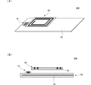
- FIG. 1A is a schematic perspective view of the antenna device 101 according to the first embodiment
- FIG. 1B is a schematic cross-sectional view of a communication terminal device (a mobile communication terminal such as a mobile phone terminal) including the antenna device 101.
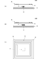
- 2A is a front view of the antenna device 101
- FIG. 2B is a partial plan view of the antenna device 101.
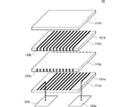
- FIG. 3 is an exploded perspective view of the feeding coil 10.
- FIG. 4 is an exploded perspective view of the coil antenna 20 and the ferrite sheet 30.
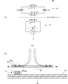
- FIG. 5A is an equivalent circuit diagram in a state where the feeding circuit 9 is connected to the antenna device 101.
- FIG. 5B is a diagram showing an induced magnetic field formed between the antenna on the communication partner side and the coil antenna 20.
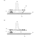
- FIG. 6A and 6B are diagrams showing the induction magnetic field of the antenna device to be compared with the antenna device of the present invention.
- FIG. 7 is a diagram showing changes in the resonance frequency of the coil antenna and the feeding coil when the thickness of the ferrite sheet 30 is changed.
- FIG. 8A is a schematic perspective view of the antenna device 102 according to the second embodiment, and FIG. 8B is a front view of the antenna device 102.
- FIG. 9A is a schematic perspective view of the antenna device 103 according to the third embodiment, and FIG. 9B is a partial plan view of the antenna device 103.
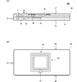
- FIG. 10A is a schematic cross-sectional view of the communication terminal device 203 including the antenna device 103.
- FIG. 10B is a plan view of the antenna device 103 in the communication terminal device 203.
- FIG. 11A is a schematic perspective view of the antenna device 104 according to the fourth embodiment, and FIG. 11B is a front view of the antenna device 104.
- 12A is a schematic perspective view of the antenna device 105A of the fifth embodiment
- FIG. 12B is a schematic perspective view of the antenna device 105B of the fifth embodiment
- FIG. 12C is a partial plan view of the antenna devices 105A and 105B.
- FIG. FIG. 13 is a partial plan view of a communication terminal device 206 including the antenna device according to the sixth embodiment.
- FIG. 14A is a schematic perspective view of the antenna device 107 according to the seventh embodiment, and FIG.
- FIG. 14B is a front view of the antenna device 107.
- FIG. 15 is a diagram illustrating an angular relationship between the communication terminal device 207 including the antenna device 107 and the communication partner side coil antenna.
- FIG. 16A is a plan view of the antenna device 108 according to the eighth embodiment, FIG. 16B is a partial plan view thereof, and FIG. 16C is a cross-sectional view of the CC portion of FIG. 16B.
- FIG. 17A is a diagram showing the induction magnetic field of the antenna device when the permeability of the ferrite sheet 30 (magnetic layer) is high or the thickness of the ferrite sheet 30 is thick, and FIG.
- FIG. 19A is a perspective view of the coil antenna 20 of the antenna device according to the tenth embodiment, and FIG. 19B is an exploded perspective view thereof.
- 20A is a plan view of the coil antenna 20, and FIG. 20B is an equivalent circuit diagram of the coil antenna 20.
- 21A and 21B are plan views of the coil antenna according to the eleventh embodiment.
- 22A is a plan view and a front view of the antenna device according to Example 12, and
- FIG. 22B is a relationship between the dimension Y from the end of the ferrite sheet 30 to one end of the feeding coil 10 and the maximum communicable distance.
- FIG. FIG. 23 is a front view of the antenna device according to the twelfth embodiment.
- the antenna device of the present invention is an antenna device used in an HF band RFID system or the like, and includes a power supply coil connected to a power supply circuit and a coil antenna disposed close to the power supply coil.
- a communication terminal device according to the present invention is a communication terminal device including the antenna device described above, and is disposed in proximity to a power feeding circuit provided in a housing, a power feeding coil connected to the power feeding circuit, and the power feeding coil. And a coil antenna.
- a magnetic layer such as a ferrite sheet is provided between the feeding coil and the coil antenna, and the feeding coil and the coil antenna have a magnetic field via the magnetic layer.
- the feeding coil and the coil antenna are magnetically coupled via the magnetic layer, and this magnetic layer satisfies the product of the relative permeability and thickness (unit: millimeter) of the magnetic body of less than 20. It is stipulated in. For this reason, even if the feeding coil and the coil antenna are arranged close to each other, the degree of coupling (coupling coefficient) does not become too large, and the degree of coupling can be maintained in an appropriate range, and the resonance between the feeding coil and the coil antenna can be maintained. It is possible to avoid separating the points greatly. Therefore, impedances of the power feeding circuit and the antenna device are matched, high-frequency signal transmission efficiency is high, and a small antenna device and a communication terminal device having a large communication distance can be realized.
- the magnetic layer does not completely shield the feeding coil and the coil antenna, but is configured to partially transmit the magnetic field component at the carrier frequency. Therefore, when using a magnetic layer having a high magnetic permeability such as a ferrite sintered body, it is necessary to magnetically couple the feeding coil and the coil antenna through the magnetic layer, and thus it is necessary to use a thin magnetic layer. is there.
- the product of the relative permeability and the thickness (unit: millimeter) of the magnetic layer is set to less than 20.
- the thickness of the magnetic layer is preferably 300 ⁇ m or less.
- the antenna device If it exceeds 300 ⁇ m, it becomes difficult to make the product of the relative permeability and the thickness of the magnetic layer (unit: millimeters) less than 20 due to the relative permeability, and if the thickness is increased, the antenna device is downsized. It is because it will inhibit.
- the power supply circuit is a functional circuit for generating a high-frequency signal and supplying it to the coil antenna.
- an RFID IC chip corresponds to this.
- the IC chip for RFID is a semiconductor integrated circuit having an RF circuit, a memory circuit, a logic circuit, and the like.
- This RFID IC chip is configured as a silicon semiconductor element or a GaAs semiconductor element.
- This semiconductor element may be configured as a bare chip IC or may be configured as a package IC.
- the feeding coil has a coil pattern connected to the feeding circuit.
- This coil pattern is constituted by at least one coil conductor.
- the coil pattern may be one in which the coil conductor is wound a plurality of turns or may be wound only for one turn.
- the coil pattern may be a laminated coil pattern in which a plurality of layers of coil conductors are connected.
- the feeding coil may include a magnetic core made of a ferrite sintered body or the like. When transmitting a high-frequency signal, the feeding coil transmits the high-frequency signal to the coil antenna via a magnetic field. At the time of reception, a high frequency signal is received from the coil antenna via a magnetic field.
- the power feeding coil and the coil antenna do not necessarily overlap each other, and may be close to each other. However, it is preferable that one of the end portions of the power supply coil is disposed so as to overlap the outside of the magnetic layer and the other overlaps the inside of the magnetic layer.
- the feeding coil is preferably arranged so that its winding axis crosses the winding axis of the coil antenna. More specifically, it is preferable that the winding axis of the feeding coil and the winding axis of the coil antenna are arranged so as to be substantially orthogonal. In particular, when it is arranged so that at least a part of the feeding coil overlaps with a coil conductor constituting the coil antenna, when viewed in plan from the winding axis direction of the coil antenna, It is preferable that the feeding coil is disposed so as to be substantially orthogonal to the winding axis. This is because the degree of coupling with respect to changes in the distance between the feeding coil and the coil antenna is stabilized.
- the feeding coil preferably has an inductance value such that a resonance circuit having a resonance frequency corresponding to the carrier frequency is formed by the feeding coil and the feeding circuit. That is, if the power supply circuit is an IC chip, it is preferable that an LC parallel resonance circuit is constituted by the capacitance of the IC chip itself and the inductance of the power supply coil, and the resonance frequency is a frequency corresponding to the carrier frequency of the communication signal. . By configuring a resonance circuit that resonates at the carrier frequency with the feeding circuit and the feeding coil, the design of the resonance frequency of the antenna device is facilitated.
- the winding axis of the power supply coil is substantially perpendicular to the end surface of the casing. It is preferable that it is arrange
- the coil antenna is disposed close to the feeding coil and is composed of at least one coil conductor.
- the coil conductor may be wound a plurality of turns or may be formed over a plurality of layers.
- the coil antenna is preferably a planar coil having a first main surface and a second main surface.
- a coil antenna can be provided in a slight space between the casing and various components provided in the casing.
- the planar coil may have a plurality of planes on its coil surface.
- the magnetic layer is preferably provided so as to cover the second main surface of the planar coil.
- a communication terminal device such as a mobile phone corresponds to a metal body having a relatively large area (such as a “conductor layer” recited in the claims), such as a ground conductor of a printed wiring board or a metal cover of a battery. ) Is provided.
- a coil antenna is disposed in the vicinity of such a metal body, an eddy current flows through the metal body so as to cancel the change in magnetic flux generated by the coil antenna, so that energy loss (eddy current loss) increases and sufficient Communication distance may not be secured. Therefore, by providing a magnetic layer between the second main surface of the planar coil and the metal body, the coupling amount between the planar coil and the feeding coil can be controlled, and the communication distance can be reduced due to eddy current loss. Can be prevented.
- the coil antenna is preferably a resonance circuit having a resonance frequency corresponding to the carrier frequency of the communication signal.
- the coil antenna can be configured by an LC parallel resonance circuit of a coil conductor having a predetermined inductance and a chip capacitor having a predetermined capacitance.
- the first coil conductor and the second coil conductor are overlapped with each other through an insulator layer so that the currents flowing through these coil conductors are in the same direction, and the inductance of each coil conductor itself is placed between each coil conductor.
- An LC parallel resonant circuit may be configured with the generated stray capacitance. Since the coil antenna can be said to be a booster antenna, it is not always necessary to have a resonance frequency corresponding to the carrier frequency of the communication signal. However, when the coil antenna resonates at a frequency corresponding to the carrier frequency, energy loss is caused. As a result, the communication distance can be increased.
- the coil antenna need not be a planar coil having a single plane, and may be a planar coil having at least a first plane and a second plane connected to the first plane, for example. In this case, it is preferable that the power feeding coil is disposed in a region surrounded by the first plane and the second plane.
- the casing of the communication terminal device has a shape having a main surface and an end (tip surface)
- the first plane is substantially parallel to the main surface of the casing
- the second plane is the end of the casing. It is preferably bent in the (tip surface) direction.
- the antenna device and communication terminal device of this invention are not limited to said embodiment.
- the antenna device of the present invention is not limited to the HF band RFID system antenna device, and can be used for various frequency bands and various communication systems such as a UHF band communication system.
- this antenna device when this antenna device is used as an antenna for an RFID system, it can be used as an antenna for a reader / writer or an antenna for an RFID tag.
- the antenna device and the communication terminal device according to the first embodiment are an antenna device for an HF band RFID system having a carrier frequency of 13.56 MHz and a mobile communication terminal equipped with the antenna device.
- 1A is a schematic perspective view of the antenna device 101 according to the first embodiment
- FIG. 1B is a schematic cross-sectional view of a communication terminal device (a mobile communication terminal such as a mobile phone terminal) including the antenna device.
- 2A is a front view of the antenna device 101
- FIG. 2B is a partial plan view of the antenna device 101.
- the antenna device 101 includes a power feeding coil 10 connected to a power feeding circuit, a coil antenna 20 disposed close to the power feeding coil 10, and a power feeding coil 10 and a coil antenna 20.
- the ferrite sheet 30 provided between the two is provided.
- the antenna device 101 also includes a printed wiring board 50.
- the feeding coil 10 is mounted on the printed wiring board 50.
- the feeding coil 10 is formed by forming a coil pattern 12 on a magnetic core 11. A specific configuration will be described later.
- the ferrite sheet 30 has a relative permeability of 50 and a thickness of 0.3 mm, and the product of the relative permeability and the thickness is 15 (less than 20).
- the coil antenna 20 includes a base sheet 21, a coil conductor 22a formed on the upper surface of the base sheet 21, and a coil conductor 22b formed on the lower surface.
- the communication terminal device 201 has a substantially rectangular parallelepiped terminal housing 60, and the antenna device 101 is provided in the terminal housing 60.
- An RFID IC chip 90 and the power feeding coil 10 are disposed in the vicinity of the tip of the printed wiring board 50.
- An RFID IC chip 90 is connected to the feeding coil 10.
- the coil antenna 20 is affixed to the inner surface of the terminal housing 60 on the back surface LF side via a bonding material 40 such as a double-sided adhesive sheet.
- the printed wiring board 50 is made of a thermosetting resin such as an epoxy resin, and its planar shape is substantially rectangular.
- the printed wiring board 50 includes a base material 51 and various conductor patterns.
- a ground conductor 52 having substantially the same shape as the planar shape of the printed wiring board is formed on the inner layer of the substrate 51.
- the ground conductor 52 functions as a ground electrode of various electronic components (not shown) such as a high-frequency circuit, a power supply circuit, and a liquid crystal driving circuit built in the communication terminal.
- FIG. 3 is an exploded perspective view of the feeding coil 10.
- the feeding coil 10 is obtained by winding a coil pattern around a magnetic core made of a ferrite sintered body.
- the magnetic core is composed of a magnetic layer 112a and a magnetic layer 112b, and the element body of the feeding coil is sandwiched between the magnetic layers 112a and 112b by the nonmagnetic layers 111a and 111b.
- An in-plane conductor 121a that is part of the coil pattern is formed on the nonmagnetic layer 111a.
- An in-plane conductor 121b that is part of the coil pattern is formed on the magnetic layer 112b.
- End face conductors 122a and 122b which are part of the coil pattern, are formed on both end faces of the magnetic layers 112a and 112b, respectively.
- Input / output terminals 123a and 123b are formed on the lower surface of the nonmagnetic layer 111a.
- a via-hole conductor is formed in the nonmagnetic layer 111a to connect the in-plane conductor 121a and the input / output terminals 123a and 123b.
- the end face conductors 122a and 122b are half (one-sided) of the through-hole conductor or via-hole conductor in which the conductor film is formed on the inner surface in the mother substrate state.
- the in-plane conductors 121a and 121b and the end surface conductors 122a and 122b constitute a coil pattern of the feeding coil.
- the magnetic layers 112a and 112b and the nonmagnetic layers 111a and 111b are ferrite ceramic sintered body layers, and the in-plane conductors 121a and 121b and end surface conductors (through-hole conductors and via-hole conductors) 122a and 122b are precursors of the ceramic sintered body layer.
- This is a sintered body of a conductive material mainly composed of silver, copper, or the like printed or filled on a ceramic green sheet.
- the feeding coil 10 is configured as a chip component having a laminated structure as a base body, and is surface-mounted on the printed wiring board 50 via the input / output terminals 123a and 123b. As shown in FIG. 2B, the feeding coil 10 is configured so that the coil pattern of the feeding coil 10 overlaps with a coil conductor constituting the coil antenna 20 when viewed in plan from the winding axis direction of the coil antenna 20. In addition, it is surface-mounted on a printed wiring board.
- FIG. 4 is an exploded perspective view of the coil antenna 20 and the ferrite sheet 30.
- the coil antenna 20 includes a base sheet 21 such as PET, a coil conductor 22a formed on the top surface of the base sheet 21, and a coil conductor 22b formed on the bottom surface.
- the coil conductors 22a and 22b are thin metal films such as copper foil and aluminum foil. In this example, it is a planar coil composed of the base sheet 21 and the coil conductors 22a and 22b.
- the upper surface in FIG. 4 is the first main surface facing the antenna on the communication partner side, and the lower surface is the second main surface on the opposite side.
- the coil conductor 22a and the coil conductor 22b are patterns wound so that the current flows in the same direction in each coil conductor when current flows from one end to the other end of each coil conductor.
- the coil conductors 22a and 22b are arranged so that at least a part of the coil conductors 22a and 22b overlap when viewed in plan from the winding axis direction. As a result, the coil conductors 22a and 22b are Couple through capacity.
- the ferrite sheet 30 is provided between the coil antenna 20 and the ground conductor 52, and is provided between the coil antenna 20 and the feeding coil 10. .
- the coil antenna 20 is viewed in plan so that the winding axis of the feeding coil 10 and the winding axis of the coil antenna 20 are substantially orthogonal to each other, the feeding coil 10 and the coil antenna 20
- the antenna 20 is arranged so that it partially overlaps, and two openings (both ends) of the feeding coil 10 protrude from the conductor formation region of the coil antenna 20.
- FIG. 5A is an equivalent circuit diagram in a state where the power feeding circuit 9 is connected to the antenna device 101.
- an LC parallel resonance circuit including the stray capacitance and the matching capacitor of the RFID IC chip itself and the inductance L of the power supply coil 10 is configured.
- the resonance frequency of this LC parallel resonance circuit is set to be approximately equal to the carrier frequency (13.56 MHz) of the communication signal.
- the antenna side including the coil antenna 20 has an LC parallel resonance circuit including an inductance L1 of the coil conductor 22a, an inductance L2 of the coil conductor 22b, and capacitors C1 and C2 formed between the coil conductor 22a and the coil conductor 22b. Is configured.
- the resonance frequency of this LC parallel resonance circuit is set to be approximately equal to the carrier frequency (13.56 MHz) of the communication signal.
- the feeding coil 10 and the coil antenna 20 are magnetically coupled to each other via the ferrite sheet 30. That is, the feeding coil 10 and the coil antenna 20 are magnetically coupled by a weak mutual inductance through a ferrite sheet.
- FIG. 5B is a diagram showing an induced magnetic field formed between the antenna (not shown) on the communication partner side and the coil antenna 20. Most of the induced magnetic field formed between the antenna on the communication partner side and the coil antenna 20 is guided along the upper interface of the ferrite sheet 30 as indicated by the magnetic flux ⁇ a. Some of them are led to the feeding coil 10 through the ferrite sheet 30 as indicated by the magnetic flux ⁇ b. In addition, since the ferrite sheet 30 exists between the coil antenna 20 and the ground conductor 52, it is possible to minimize the generation of eddy current in the ground conductor 52 due to the induced magnetic field of the current flowing through the coil antenna 20.
- FIG. 6 (A) and 6 (B) are diagrams showing the induction magnetic field of the antenna device as a comparison target of the antenna device of the present invention.
- FIG. 6A shows an example of an antenna device without a ferrite sheet
- FIG. 6B shows an example of an antenna device with a ferrite sheet provided at a position avoiding the feeding coil 10.
- the ferrite sheet 30 is provided in a part between the coil antenna 20 and the ground conductor 52, eddy current loss is generated as compared with the antenna device shown in FIG. However, it is inevitable that eddy current loss occurs in a portion that is not covered with the ferrite sheet 30. Further, similarly to the antenna device of FIG. 6A, there is a problem of transmission loss of signal energy due to separation of resonance points.
- FIG. 7 is a diagram showing changes in the resonance frequency of the coil antenna and the feeding coil when the thickness of the ferrite sheet 30 is changed in the structure of the antenna device 101 shown in the first embodiment.
- the conditions for obtaining the results of FIGS. 7A to 7D are as follows.
- [Ferrite sheet] ⁇ (A) to (D) correspond to FIGS. 7 (A) to (D) ⁇
- the coupling between the feeding coil 10 and the coil antenna 20 solves the degeneration and separates the resonance points, but the maximum communication distance: 37 mm is obtained. It was.
- the feeding coil 10 and the coil antenna 20 are not coupled, and only the maximum communication distance: 25 mm is obtained.
- FIG. 7D if the ferrite sheet is not provided, the coupling between the feeding coil 10 and the coil antenna 20 can largely solve the degeneracy, and the resonance point is largely separated. Since eddy current loss occurred, the maximum communication distance was 20 mm.
- Example 1 as shown in FIG. 5B and the like, the feeding coil 10 and the coil antenna 20 are arranged so that the winding axis of the feeding coil 10 and the winding axis of the coil antenna 20 are substantially orthogonal to each other.
- the coil antenna 20 is viewed in plan, the feeding coil 10 and the coil antenna 20 are partially overlapped, and the opening (end) of the feeding coil 10 protrudes from the conductor formation region of the coil antenna 20. Therefore, even when the distance between the coil antenna 20 and the power feeding coil 10 is increased, the relationship in which the magnetic flux ⁇ a is linked to the coil antenna 20 and the magnetic flux ⁇ b is linked to the power feeding coil 10 is maintained. Communication characteristics can be obtained.
- a ground conductor (conductor layer) 52 is provided so that the feeding coil 10 is sandwiched between the coil antenna 20 and the ground conductor 52 is a coil provided in the feeding coil 10. It extends along the winding axis of the pattern 12.
- the ground conductor 52 is disposed so as to cover the feeding coil 10 and to be located at least partially inside the inner circumference of the coil conductor of the coil antenna 20 in plan view.
- W10 represents the width of the feeding coil 10
- D20 represents the inner circumference of the coil conductor of the coil antenna 20.
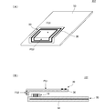
- FIG. 8A is a schematic perspective view of the antenna device 102 according to the second embodiment
- FIG. 8B is a front view of the antenna device 102.
- the feeding coil 10 is mounted on the printed wiring board 50 so that the winding axis direction is the same as the coil winding axis of the coil antenna 20.
- the configuration is the same as that of the antenna device 101 of the first embodiment except that the mounting position of the feeding coil 10 is different.
- the antenna device 102 according to the second embodiment can ensure a communication distance substantially equal to that of the antenna device 101 according to the first embodiment. However, when the distance between the feeding coil 10 and the coil antenna 20 is increased or the positional relationship is shifted, or If the resonance frequency of the coil antenna 20 varies, the resonance frequency of the antenna device may fluctuate.
- FIG. 9A is a schematic perspective view of the antenna device 103 according to the third embodiment, and FIG. 9B is a partial plan view of the antenna device 103.
- FIG. 10A is a schematic cross-sectional view of a communication terminal device 203 provided with the antenna device 103.
- FIG. 10B is a plan view of the antenna device 103 in the communication terminal device 203.
- the coil antenna 20 is disposed so as to be located at substantially the center of the terminal housing 60 when viewed from the back surface LF of the terminal housing 60.
- the feeding coil 10 is arranged so that the coil opening surface is close to the side end SE of the terminal housing 60. Therefore, even if the coil antenna 20 is disposed at the approximate center of the terminal housing 60, the magnetic flux passing through the feeding coil 10 can be turned toward the side end SE of the terminal housing 60. That is, at the time of transmission, the magnetic flux from the feeding coil 10 circulates in the direction of the side end SE, and at the time of reception, the magnetic flux from the communication partner mainly avoids the printed wiring board 50. Oriented.
- various electronic components 71 constituting the communication terminal device 203 are mounted as surface-mounted components on the printed wiring board 50 arranged in the terminal housing 60.
- a battery pack 72 is disposed in the vicinity of the coil antenna 20.
- a ferrite sheet 30 is attached to the entire surface of the second main surface of the coil antenna 20. Therefore, even if a metal body other than the ground conductor 52 (for example, various electronic components 71 and the battery pack 72) is disposed in the vicinity of the coil antenna 20, eddy current loss due to these metal bodies hardly occurs. For the same reason, the fluctuation amount of the resonance frequency of the coil antenna 20 is also small.
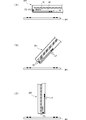
- FIG. 11A is a schematic perspective view of the antenna device 104 according to the fourth embodiment
- FIG. 11B is a front view of the antenna device 104.
- the antenna device 104 according to the fourth embodiment is disposed at a position that does not overlap the ferrite sheet 30 when the feeding coil 10 is viewed in plan from the winding axis direction of the coil antenna 20. Even in this case, since the feeding coil 10 is disposed on the opposite side of the coil antenna 20 with respect to the plane including the ferrite sheet 30, the feeding coil 10 and the coil antenna 20 are magnetic fields via the ferrite sheet 30. Join. That is, the feeding coil 10 and the coil antenna 20 are magnetically coupled by the magnetic flux that has passed through the ferrite sheet 30.
- FIG. 12A is a schematic perspective view of the antenna device 105A of the fifth embodiment
- FIG. 12B is a schematic perspective view of the antenna device 105B of the fifth embodiment
- FIG. 12C is a partial plan view of the antenna devices 105A and 105B.
- the feeding coil 10 is disposed at a substantially central portion of the coil opening of the coil antenna 20 when viewed in plan from the winding axis direction of the coil antenna 20.
- the feeding coil 10 may be disposed so that the winding axis of the feeding coil 10 and the winding axis of the coil conductor of the coil antenna 20 are substantially orthogonal to each other.
- the winding axis of the feeding coil 10 and the winding axis of the coil conductor of the coil antenna 20 are arranged substantially parallel to each other, and further, the both winding axes are arranged to be the same. May be.
- FIG. 13 is a partial plan view of the communication terminal device 206 including the antenna device of the sixth embodiment.
- the coil antenna 20 and the ferrite sheet 30 are arranged so as to avoid the camera module 73 and the speaker 74.
- the coil antenna 20 and the ferrite sheet 30 do not have to have a rectangular outer shape as in the other embodiments, and may have a concave portion or a convex portion.
- FIG. 14A is a schematic perspective view of the antenna device 107 according to the seventh embodiment
- FIG. 14B is a front view of the antenna device 107
- FIG. 15 is a diagram illustrating an angular relationship between the communication terminal device 207 including the antenna device 107 and the communication partner side coil antenna.
- the coil antenna 20 has a first plane FS1 and a second plane FS2 connected to the first plane FS1. It is a planar coil.
- the ferrite sheet 30 has a first plane FS1 and a second plane FS2, and is provided so as to cover all of the coil conductor of the coil antenna 20 and its opening surface.
- the feeding coil 10 is disposed in a region surrounded by the first plane FS1 and the second plane FS2 of the coil antenna 20 and the ferrite sheet 30.
- the first plane FS1 is a plane substantially parallel to the main surface of the terminal housing 60, and the second plane FS2 is bent along the surface of the tip FE of the terminal housing 60.
- the angle formed by the first plane FS1 and the second plane FS2 is approximately 90 °, but may be an obtuse angle such as 120 ° or an acute angle such as 45 °. It may be. Also, instead of configuring the first plane FS1 and the second plane FS2 with a predetermined bending angle, the first plane FS1 and the second plane FS2 may be connected by a curved surface, The portions corresponding to the flat surface FS1 and the second flat surface FS2 may be configured by one curved surface.
- FIG. 16 is a plan view of the antenna device 108 according to the eighth embodiment, FIG. 16B is a partial plan view thereof, and FIG. 16C is a cross-sectional view of the CC portion of FIG. 16B.
- the feeding coil 10 is disposed outside the formation region of the coil conductors 22 (22a, 22b) of the coil antenna 20.
- an extending portion 22E is formed at a part of the outer edge of the coil conductor 22 (22a, 22b), and the feeding coil 10 is arranged at a position where the feeding coil 10 overlaps the extending portion 22E.
- the ferrite sheet 30 is also extended so as to overlap the extended portion 22E.
- the feeding coil 10 is arranged outside the coil conductor 22 (22a, 22b), the degree of coupling between the feeding coil 10 and the coil antenna 20 may become too small. However, as in this embodiment, the feeding coil It is preferable to provide an extended portion on a part of the coil antenna 20 and a part of the ferrite sheet 30 so as to overlap with 10.
- Example 9 shows the relationship between the magnetic permeability, thickness, and communication distance of the magnetic layer.
- FIG. 17A is a diagram showing an induction magnetic field of the antenna device when the permeability of the ferrite sheet 30 (magnetic layer) is high or when the thickness of the ferrite sheet 30 is thick.
- FIG. 17B is a diagram showing an induction magnetic field of the antenna device when the permeability of the ferrite sheet 30 (magnetic layer) is low or the thickness of the ferrite sheet 30 is thin.
- the magnetic field coupling between the magnetic flux ⁇ a from the communication partner and the coil antenna 20 increases as shown in FIG.
- the magnetic field coupling indicated by the magnetic flux ⁇ b between the antenna 20 and the feeding coil 10 becomes small. As a result, the maximum communicable distance is short.
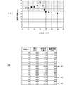
- FIG. 18A is a diagram showing the relationship of the maximum communication distance with respect to the product of the relative permeability (actual permeability ⁇ ′) and the thickness of the ferrite sheet 30.
- FIG. 18B is a numerical table. The conditions for obtaining this result are as follows.
- Example 10 shows optimization of the coil conductor pattern of the coil antenna.
- FIG. 19A is a perspective view of the coil antenna 20, and FIG. 19B is an exploded perspective view thereof.
- 20A is a plan view of the coil antenna 20, and
- FIG. 20B is an equivalent circuit diagram of the coil antenna 20.
- a first coil conductor 22a is formed on a first main surface (upper surface) of a base material sheet 21 such as PET, and a second main surface (lower surface) second coil conductor 22b is formed. Since the winding direction of the first coil conductor 22a and the winding direction of the second coil conductor 22b are opposite (the same in a transparent state), an equivalent circuit is as shown in FIG.
- inductors L1 and L2 correspond to the coil conductors 22a and 22b
- the capacitor C1 is a capacitance generated mainly near the outer peripheral ends of the coil conductors 22a and 22b
- the capacitor C2 is the main conductor of the coil conductors 22a and 22b. It is a capacitance generated near the inner peripheral ends.
- the design is such that C1 >> C2 ⁇ 0. Since the capacitor C2 portion is almost open, almost no current flows through the electrode near C2. That is, the electric field is maximized.
- the electrode near the capacitor C1 farthest from the electrode near the capacitor C2 is the maximum current point. That is, the amount of current flowing through the coil conductors 22a and 22b is large on the outside and small on the inside.
- the magnetic field generation region is located on the outermost side of the coil antenna 20, which means that the equivalent antenna size is large, and thus an antenna with good radiation efficiency can be obtained.
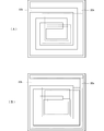
- Example 11 shows another two patterns of the coil conductor of the coil antenna.
- FIG. 21A and FIG. 21B are plan views of the coil antenna, respectively.
- the capacity is larger toward the outside of the coil conductors 22a and 22b, and the capacity is smaller toward the inside.
- the capacitance is adjusted by gradually changing the line width of the coil conductor. That is, the line width of the coil conductor 22a is made the same, and the line width of the coil conductor 22b is reduced from the outer periphery to the inner periphery.
- the line widths of the opposing portions of the coil conductors 22a and 22b are made thinner (the amount of deviation is increased) from the outer periphery of the coil to the inner periphery.
- Example 12 shows the relationship between the positional relationship between one end of the feeding coil 10 and the ferrite sheet and the maximum communicable distance.
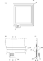
- FIG. 22A is a plan view and a front view of the antenna device
- FIG. 22B is a diagram showing the relationship between the dimension Y from the end of the ferrite sheet 30 to one end of the feeding coil 10 and the maximum communicable distance. .
- the conditions for obtaining this result are as follows.
- FIG. 23 is a front view of the antenna device.
- the magnetic flux from the feeding coil 10 circulates outside the coil antenna 20.
- the distribution is such that the parts are interlinked. Therefore, the feeding coil 10 and the coil antenna 20 can be more strongly coupled.
- FIG. 23B when the opening of the feeding coil 10 does not come out of the outer shape of the coil antenna 20, the magnetic flux from the feeding coil 10 is affected by the ferrite sheet 30 and the opening of the coil antenna 20.
- the distribution is such that they do not interlink. For this reason, the coupling between the feeding coil 10 and the coil antenna 20 is slightly weaker than the above.
- the feeding coil 10 and the coil antenna 20 partially overlap, and the opening (end) of the feeding coil 10 protrudes from the outer shape of the coil antenna 20.
- the coupling between the feeding coil 10 and the coil antenna 20 becomes strong, and stable communication characteristics can be obtained even if the distance between the coil antenna 20 and the feeding coil 10 is increased.
- the “conductor layer” is a ground conductor of a printed wiring board is mainly shown, but a conductor plate such as a liquid crystal panel, a battery pack, or a shield case is used as the “conductor layer”. It is also possible to apply.
- the present invention can be used for antenna devices and communication terminal devices, particularly antenna devices used for HF band RFID tags, reader / writers, etc., and communication terminal devices equipped with this antenna device. This is useful for RFID systems for management.
Landscapes
- Engineering & Computer Science (AREA)
- Physics & Mathematics (AREA)
- Computer Networks & Wireless Communication (AREA)
- Electromagnetism (AREA)
- Microelectronics & Electronic Packaging (AREA)
- General Physics & Mathematics (AREA)
- Theoretical Computer Science (AREA)
- Health & Medical Sciences (AREA)
- Toxicology (AREA)
- Computer Hardware Design (AREA)
- General Health & Medical Sciences (AREA)
- Artificial Intelligence (AREA)
- Computer Vision & Pattern Recognition (AREA)
- Details Of Aerials (AREA)
- Support Of Aerials (AREA)
- Variable-Direction Aerials And Aerial Arrays (AREA)
- Near-Field Transmission Systems (AREA)
Abstract
Description
(A)実部透磁率μ’=70、厚みδ=50μm [磁性体の比透磁率と厚み(単位はミリメートル)との積=3.5]
(B)実部透磁率μ’=70、厚みδ=100μm [磁性体の比透磁率と厚み(単位はミリメートル)との積=7]
(C)実部透磁率μ’=70、厚みδ=500μm [磁性体の比透磁率と厚み(単位はミリメートル)との積=35]
(D)フェライトシート無し
[給電コイル]
インダクタンス0.74μH
[コイルアンテナ]
平面寸法:40mmx40mm
厚み:100μm
[RFID用ICチップ]
NXP社製PN-544
[リーダライタ]
VIVOtech社製VIVO5000
図7(A)~(D)において、曲線sは、給電コイル10単独の状態での周波数特性であり、曲線dは給電コイル10とコイルアンテナ20とが結合している状態での周波数特性である。コイルアンテナ20単独での周波数特性も曲線sと同等である。
外形40mm×40mm
3ターン×両面
線幅=1mm
線間=1mm
[フェライトシート]
サイズはコイルアンテナの外形と同じ
[通信相手のカード]
ISO14443A規格の一般的なカード(80mm×50mm程度の大きさ)
図18(A)、図18(B)に示すように、フェライトシート30の比透磁率と厚みの積が20未満であれば、通信可能最大距離:30mmを確保できる。通信可能最大距離:30mm以上の場合、アンテナ装置を端末筐体内部に配置し、端末筐体の厚みを介して通信する場合や、通信相手先との間に多少の隙間が発生した場合も安定した通信を行うことができる。
平面寸法:40mm×40mm
厚み:50μm
6ターン×両面
線幅=1mm
線間=0.5mm
[フェライトシート]
平面寸法:40mm×40mm
厚み:100μm
比透磁率:約130
[プリント配線板]
平面寸法:50mm×110mm
[給電コイル]
平面寸法:5mm×5mm
厚み:0.8μm
[フェライトシートとプリント配線板との間隔]
1.2mm
図22(B)に表れているように、フェライトシート30の端部から給電コイル10の一端までの寸法Yが0mm、35~40mmであるとき、最も良好な特性が得られる。
FS1…第1の平面
FS2…第2の平面
LF…裏面
TF…表面
SE…側端部
9…給電回路
10…給電コイル
11…磁性体コア
12…コイルパターン
20…コイルアンテナ
21…基材シート
22…コイル導体
22a…第1コイル導体
22b…第2コイル導体
22E…延設部
30…フェライトシート
40…接合材
50…プリント配線板
51…基材
52…グランド導体
60…端末筐体
71…電子部品
72…バッテリーパック
73…カメラモジュール
74…スピーカ
90…RFID用ICチップ
101~104…アンテナ装置
105A,105B…アンテナ装置
107,108…アンテナ装置
111a,111b…非磁性層
112a,112b…磁性層
121a,121b…面内導体
122a,122b…端面導体
123a,123b…入出力端子
201,203,206,207…通信端末装置
301…通信相手側コイルアンテナ
Claims (14)
- 給電回路に接続される給電コイルと、前記給電コイルに近接配置されたコイルアンテナと、を有するアンテナ装置であって、
前記給電コイルと前記コイルアンテナとの間に、磁性体の比透磁率と厚み(単位はミリメートル)との積が20未満の磁性体層が設けられており、前記給電コイルと前記コイルアンテナとは、前記磁性体層を介して磁界結合されている、ことを特徴とするアンテナ装置。 - 前記コイルアンテナは通信相手側のアンテナに向く面である第1主面とこの第1主面の反対面である第2主面とを有する平面状のコイルであり、前記磁性体層は前記コイルアンテナの第2主面を覆うように設けられている、請求項1に記載のアンテナ装置。
- 前記コイルアンテナは、第1主面に形成された平面状の第1コイル導体および第2主面に形成された平面状の第2コイル導体で構成されていて、
前記第1コイル導体のインダクタンス、前記第2コイル導体のインダクタンス、および前記第1コイル導体と前記第2コイル導体との間に生じる容量によりLC並列共振回路が構成されていて、
前記コイルアンテナの平面視で、前記第1コイル導体と前記第2コイル導体との対向面積は、第1コイル導体および第2コイル導体の外周端部付近で最も大きく、内周端部で最も小さい、請求項2に記載のアンテナ装置。 - 導体層を有し、前記磁性体層は前記コイルアンテナの前記第2主面と前記導体層との間に設けられている、請求項2または3に記載のアンテナ装置。
- 前記コイルアンテナの平面視で、前記給電コイルは、その少なくとも一部が前記磁性体層に重なるように配置されている、請求項1~4のいずれかに記載のアンテナ装置。
- 前記給電コイルは、その巻回軸が前記コイルアンテナの巻回軸に対しほぼ直交するように配置されている、請求項1~5のいずれかに記載のアンテナ装置。
- 前記コイルアンテナは、通信信号のキャリア周波数に実質的に相当する共振周波数を持つ共振回路である、請求項1~6のいずれかに記載のアンテナ装置。
- 前記給電コイルと前記給電回路とで、通信信号のキャリア周波数に相当する周波数で共振する共振回路が構成されている、請求項1~7のいずれかに記載のアンテナ装置。
- 前記コイルアンテナは、少なくとも第1の平面と前記第1の平面に連接した第2の平面とを有する平面状のコイルであり、前記給電コイルは、前記第1の平面と前記第2の平面とで囲まれた領域に配置されている、請求項1~8のいずれかに記載のアンテナ装置。
- 前記磁性体層は、その厚みが300μm以下である、請求項1~9のいずれかに記載のアンテナ装置。
- 筐体と、前記筐体内に設けられた給電回路と、前記給電回路に接続された給電コイルと、前記給電コイルに近接配置されたコイルアンテナと、を有する通信端末装置であって、
前記給電コイルと前記コイルアンテナとの間に磁性体層を備え、前記給電コイルと前記コイルアンテナとは、前記磁性体層を介して電磁界結合されている、ことを特徴とする通信端末装置。 - 前記給電コイルは、前記給電コイルの巻回軸が前記筐体の端面に対してほぼ垂直を向く状態で前記筐体内の端部近傍に配置されている、請求項11に記載の通信端末装置。
- 前記コイルアンテナは、少なくとも第1の平面と前記第1の平面に連接した第2の平面を有する平面状コイルであり、前記第1の平面は前記筐体の主面に対してほぼ平行であり、前記第2の平面は前記筐体の端部方向に折り曲げられている、請求項11または12に記載の通信端末装置。
- 前記コイルアンテナとで給電コイルを挟むように、前記給電コイルの巻回軸に沿って延びる導体層を備え、前記導体層は、平面視で、給電コイルを覆い且つ少なくとも一部が前記コイルアンテナのコイル導体の内周より内側に位置するように配置されている、請求項11~13のいずれかに記載の通信端末装置。
Priority Applications (5)
| Application Number | Priority Date | Filing Date | Title |
|---|---|---|---|
| CN201280021203.8A CN103503234B (zh) | 2011-06-13 | 2012-06-11 | 天线装置及通信终端装置 |
| GB1319328.9A GB2505577B (en) | 2011-06-13 | 2012-06-11 | Antenna device comprising a feed coil coupled to a coil antenna via a magnetic layer |
| JP2013509359A JP5293907B2 (ja) | 2011-06-13 | 2012-06-11 | アンテナ装置および通信端末装置 |
| US14/066,793 US20140176382A1 (en) | 2011-06-13 | 2013-10-30 | Antenna device and communication terminal apparatus |
| US15/014,179 US9847578B2 (en) | 2011-06-13 | 2016-02-03 | Antenna device and communication terminal apparatus |
Applications Claiming Priority (4)
| Application Number | Priority Date | Filing Date | Title |
|---|---|---|---|
| JP2011131193 | 2011-06-13 | ||
| JP2011-131193 | 2011-06-13 | ||
| JP2012-038983 | 2012-02-24 | ||
| JP2012038983 | 2012-02-24 |
Related Child Applications (1)
| Application Number | Title | Priority Date | Filing Date |
|---|---|---|---|
| US14/066,793 Continuation US20140176382A1 (en) | 2011-06-13 | 2013-10-30 | Antenna device and communication terminal apparatus |
Publications (1)
| Publication Number | Publication Date |
|---|---|
| WO2012173080A1 true WO2012173080A1 (ja) | 2012-12-20 |
Family
ID=47357067
Family Applications (1)
| Application Number | Title | Priority Date | Filing Date |
|---|---|---|---|
| PCT/JP2012/064888 Ceased WO2012173080A1 (ja) | 2011-06-13 | 2012-06-11 | アンテナ装置および通信端末装置 |
Country Status (5)
| Country | Link |
|---|---|
| US (2) | US20140176382A1 (ja) |
| JP (1) | JP5293907B2 (ja) |
| CN (1) | CN103503234B (ja) |
| GB (1) | GB2505577B (ja) |
| WO (1) | WO2012173080A1 (ja) |
Cited By (11)
| Publication number | Priority date | Publication date | Assignee | Title |
|---|---|---|---|---|
| JP2014154896A (ja) * | 2013-02-04 | 2014-08-25 | Murata Mfg Co Ltd | アンテナ、アンテナ装置、及び携帯端末 |
| CN104112908A (zh) * | 2013-04-22 | 2014-10-22 | 英飞凌科技股份有限公司 | 天线装置、通信装置以及天线结构 |
| WO2014199862A1 (ja) * | 2013-06-14 | 2014-12-18 | 株式会社村田製作所 | アンテナ装置および通信端末装置 |
| WO2014199861A1 (ja) * | 2013-06-14 | 2014-12-18 | 株式会社村田製作所 | アンテナ装置および通信端末装置 |
| JP2016123112A (ja) * | 2013-09-17 | 2016-07-07 | 株式会社村田製作所 | 電子機器 |
| EP2937937A4 (en) * | 2012-12-21 | 2016-08-24 | Murata Manufacturing Co | ANTENNA DEVICE AND ELECTRONIC DEVICE |
| WO2016163437A1 (ja) * | 2015-04-08 | 2016-10-13 | 株式会社村田製作所 | アンテナ装置、カード型情報媒体、電子機器およびアンテナ装置の製造方法 |
| US9627762B2 (en) | 2013-11-08 | 2017-04-18 | Murata Manufacturing Co., Ltd. | Antenna device, communication terminal device, and communication terminal device cover |
| JP2018064151A (ja) * | 2016-10-11 | 2018-04-19 | シャープ株式会社 | アンテナ装置 |
| JP2019016868A (ja) * | 2017-07-04 | 2019-01-31 | 株式会社村田製作所 | アンテナ装置、コイルアンテナ及び電子機器 |
| US10445635B2 (en) | 2015-07-31 | 2019-10-15 | Murata Manufacturing Co., Ltd. | Feeder coil, antenna device, and electronic appliance |
Families Citing this family (27)
| Publication number | Priority date | Publication date | Assignee | Title |
|---|---|---|---|---|
| US9136600B2 (en) * | 2010-09-30 | 2015-09-15 | Murata Manufacturing Co., Ltd. | Antenna |
| CN102668241B (zh) * | 2010-03-24 | 2015-01-28 | 株式会社村田制作所 | Rfid系统 |
| WO2012144482A1 (ja) * | 2011-04-18 | 2012-10-26 | 株式会社村田製作所 | アンテナ装置および通信端末装置 |
| JP6347607B2 (ja) * | 2013-12-27 | 2018-06-27 | キヤノン株式会社 | 電子機器 |
| CN105900285B (zh) * | 2014-01-17 | 2019-11-26 | 迪睿合株式会社 | 天线装置以及电子设备 |
| EP2992776B1 (en) * | 2014-09-04 | 2019-11-06 | WITS Co., Ltd. | Case and apparatus including the same |
| CN105745788B (zh) * | 2014-09-12 | 2019-02-26 | 阿莫技术有限公司 | 多环路天线模块及具有其的可携带终端 |
| US10403979B2 (en) | 2015-03-13 | 2019-09-03 | Samsung Electro-Mechanics Co., Ltd. | Antenna apparatus and electronic device including the same |
| US20170005395A1 (en) * | 2015-06-30 | 2017-01-05 | Tdk Corporation | Antenna device |
| US20170084984A1 (en) * | 2015-09-22 | 2017-03-23 | Tabletop Media Llc D/B/A Ziosk | Booster Antenna |
| US10090592B2 (en) * | 2015-10-29 | 2018-10-02 | Sonitus Technologies Inc. | Communication device |
| ES2716882T3 (es) * | 2015-11-04 | 2019-06-17 | Premo Sa | Dispositivo de antena para operaciones de HF y LF |
| JP6251770B2 (ja) * | 2016-04-15 | 2017-12-20 | 株式会社エスケーエレクトロニクス | Rfidタグ |
| JP6727703B2 (ja) * | 2016-05-30 | 2020-07-22 | デクセリアルズ株式会社 | アンテナ装置、及び電子機器 |
| CN109565113B (zh) * | 2016-06-01 | 2021-03-30 | 户田工业株式会社 | 天线装置以及使用其的ic标签 |
| US9941937B1 (en) * | 2017-04-10 | 2018-04-10 | Nxp B.V. | Near-field electromagnetic induction (NFEMI) antenna |
| KR102245948B1 (ko) * | 2017-06-12 | 2021-04-30 | 삼성전자주식회사 | 안테나 및 안테나를 포함하는 전자 장치 |
| KR101883109B1 (ko) * | 2017-07-20 | 2018-07-27 | 삼성전기주식회사 | 안테나 모듈 |
| US10726323B2 (en) * | 2018-05-31 | 2020-07-28 | Toshiba Memory Corporation | Semiconductor storage device |
| WO2020003568A1 (ja) * | 2018-06-25 | 2020-01-02 | 株式会社村田製作所 | Rfidタグ及びrfid付き物品 |
| SK289250B6 (sk) * | 2018-08-02 | 2024-10-23 | Logomotion, S.R.O. | Anténová sústava aspoň s dvoma anténami, najmä na NFC prenos |
| TWM573545U (zh) * | 2018-09-18 | 2019-01-21 | 振鋒企業股份有限公司 | 用於設置在一金屬物件上的近場通訊數據載體 |
| KR102176235B1 (ko) * | 2019-03-28 | 2020-11-09 | 코나엠 주식회사 | 양방향 통신이 가능한 메탈 카드 및 메탈 카드 제조 방법 |
| US11764462B2 (en) * | 2020-08-11 | 2023-09-19 | BCS Access Systems US, LLC | Vehicle door handle |
| KR102752195B1 (ko) * | 2020-09-16 | 2025-01-10 | 삼성전자주식회사 | 패치 안테나 및 코일 안테나를 포함하는 전자 장치 |
| JP7651373B2 (ja) * | 2021-05-24 | 2025-03-26 | Tdk株式会社 | アンテナ装置及びこれを備えるワイヤレス電力伝送デバイス |
| CN116119473B (zh) * | 2022-12-28 | 2025-08-26 | 广州鲁邦通物联网科技股份有限公司 | 一种楼层和平层识别系统和识别方法 |
Citations (5)
| Publication number | Priority date | Publication date | Assignee | Title |
|---|---|---|---|---|
| JP3123411U (ja) * | 2006-05-02 | 2006-07-20 | 株式会社スマート | 金属片付タグおよび/またはセンサを用いたシステム |
| JP2009021970A (ja) * | 2007-06-11 | 2009-01-29 | Tamura Seisakusho Co Ltd | ブースターアンテナコイル |
| JP2010171857A (ja) * | 2009-01-26 | 2010-08-05 | Murata Mfg Co Ltd | アンテナ装置 |
| JP2010268286A (ja) * | 2009-05-15 | 2010-11-25 | Murata Mfg Co Ltd | 磁性体アンテナ及びアンテナ装置 |
| WO2011002050A1 (ja) * | 2009-07-03 | 2011-01-06 | 株式会社村田製作所 | アンテナモジュール |
Family Cites Families (7)
| Publication number | Priority date | Publication date | Assignee | Title |
|---|---|---|---|---|
| US4583099A (en) * | 1983-12-27 | 1986-04-15 | Polyonics Corporation | Resonant tag circuits useful in electronic security systems |
| GB2384627B (en) * | 2000-10-04 | 2004-09-08 | Motorola Inc | Folded inverted F antenna for GPS applications |
| JP2004253858A (ja) * | 2003-02-18 | 2004-09-09 | Minerva:Kk | Icタグ用のブースタアンテナ装置 |
| US7699231B2 (en) * | 2003-08-13 | 2010-04-20 | Murata Manufacturing Co., Ltd. | Reader/writer and mobile communication apparatus |
| NL1030077C2 (nl) * | 2005-09-30 | 2007-04-02 | Nedap Nv | Verbeterd resonantielabel met verdeelde capaciteit. |
| JP4955465B2 (ja) * | 2007-06-11 | 2012-06-20 | 株式会社タムラ製作所 | ブースターアンテナ |
| EP3057178A1 (en) * | 2009-09-25 | 2016-08-17 | Murata Manufacturing Co., Ltd. | Antenna device and mobile terminal |
-
2012
- 2012-06-11 GB GB1319328.9A patent/GB2505577B/en active Active
- 2012-06-11 JP JP2013509359A patent/JP5293907B2/ja active Active
- 2012-06-11 WO PCT/JP2012/064888 patent/WO2012173080A1/ja not_active Ceased
- 2012-06-11 CN CN201280021203.8A patent/CN103503234B/zh active Active
-
2013
- 2013-10-30 US US14/066,793 patent/US20140176382A1/en not_active Abandoned
-
2016
- 2016-02-03 US US15/014,179 patent/US9847578B2/en active Active
Patent Citations (5)
| Publication number | Priority date | Publication date | Assignee | Title |
|---|---|---|---|---|
| JP3123411U (ja) * | 2006-05-02 | 2006-07-20 | 株式会社スマート | 金属片付タグおよび/またはセンサを用いたシステム |
| JP2009021970A (ja) * | 2007-06-11 | 2009-01-29 | Tamura Seisakusho Co Ltd | ブースターアンテナコイル |
| JP2010171857A (ja) * | 2009-01-26 | 2010-08-05 | Murata Mfg Co Ltd | アンテナ装置 |
| JP2010268286A (ja) * | 2009-05-15 | 2010-11-25 | Murata Mfg Co Ltd | 磁性体アンテナ及びアンテナ装置 |
| WO2011002050A1 (ja) * | 2009-07-03 | 2011-01-06 | 株式会社村田製作所 | アンテナモジュール |
Cited By (26)
| Publication number | Priority date | Publication date | Assignee | Title |
|---|---|---|---|---|
| EP2937937A4 (en) * | 2012-12-21 | 2016-08-24 | Murata Manufacturing Co | ANTENNA DEVICE AND ELECTRONIC DEVICE |
| US9847585B2 (en) | 2012-12-21 | 2017-12-19 | Murata Manufacturing Co., Ltd. | Antenna device and electronic apparatus |
| JP2014154896A (ja) * | 2013-02-04 | 2014-08-25 | Murata Mfg Co Ltd | アンテナ、アンテナ装置、及び携帯端末 |
| CN104112908A (zh) * | 2013-04-22 | 2014-10-22 | 英飞凌科技股份有限公司 | 天线装置、通信装置以及天线结构 |
| DE102013104059A1 (de) * | 2013-04-22 | 2014-10-23 | Infineon Technologies Ag | Antennen-Anordnung, Kommunikationsgerät und Antennenstruktur |
| DE102013104059B8 (de) | 2013-04-22 | 2024-09-19 | Infineon Technologies Ag | Antennen-Anordnung und Kommunikationsgerät |
| DE102013104059B4 (de) | 2013-04-22 | 2024-05-29 | Infineon Technologies Ag | Antennen-Anordnung und Kommunikationsgerät |
| US10096902B2 (en) | 2013-04-22 | 2018-10-09 | Infineon Technologies Ag | Antenna arrangement, communication appliance and antenna structure |
| JP5692483B1 (ja) * | 2013-06-14 | 2015-04-01 | 株式会社村田製作所 | アンテナ装置および通信端末装置 |
| JP5686232B1 (ja) * | 2013-06-14 | 2015-03-18 | 株式会社村田製作所 | アンテナ装置および通信端末装置 |
| JP2015092775A (ja) * | 2013-06-14 | 2015-05-14 | 株式会社村田製作所 | アンテナ装置および通信端末装置 |
| WO2014199862A1 (ja) * | 2013-06-14 | 2014-12-18 | 株式会社村田製作所 | アンテナ装置および通信端末装置 |
| CN104508909B (zh) * | 2013-06-14 | 2017-04-12 | 株式会社村田制作所 | 天线装置及通信终端装置 |
| US9634380B2 (en) | 2013-06-14 | 2017-04-25 | Murata Manufacturing Co., Ltd. | Antenna device and communication terminal device |
| WO2014199861A1 (ja) * | 2013-06-14 | 2014-12-18 | 株式会社村田製作所 | アンテナ装置および通信端末装置 |
| CN104508909A (zh) * | 2013-06-14 | 2015-04-08 | 株式会社村田制作所 | 天线装置及通信终端装置 |
| US10224604B2 (en) | 2013-06-14 | 2019-03-05 | Murata Manufacturing Co., Ltd. | Antenna device and communication terminal device |
| JP2016123112A (ja) * | 2013-09-17 | 2016-07-07 | 株式会社村田製作所 | 電子機器 |
| US9627762B2 (en) | 2013-11-08 | 2017-04-18 | Murata Manufacturing Co., Ltd. | Antenna device, communication terminal device, and communication terminal device cover |
| US10122065B2 (en) | 2015-04-08 | 2018-11-06 | Murata Manufacturing Co., Ltd. | Antenna device, card information medium, electronic apparatus, and method for manufacturing antenna device |
| JPWO2016163437A1 (ja) * | 2015-04-08 | 2017-06-29 | 株式会社村田製作所 | アンテナ装置、カード型情報媒体、電子機器およびアンテナ装置の製造方法 |
| WO2016163437A1 (ja) * | 2015-04-08 | 2016-10-13 | 株式会社村田製作所 | アンテナ装置、カード型情報媒体、電子機器およびアンテナ装置の製造方法 |
| US10445635B2 (en) | 2015-07-31 | 2019-10-15 | Murata Manufacturing Co., Ltd. | Feeder coil, antenna device, and electronic appliance |
| US10664738B2 (en) | 2015-07-31 | 2020-05-26 | Murata Manufacturing Co., Ltd. | Feeder coil, antenna device, and electronic appliance |
| JP2018064151A (ja) * | 2016-10-11 | 2018-04-19 | シャープ株式会社 | アンテナ装置 |
| JP2019016868A (ja) * | 2017-07-04 | 2019-01-31 | 株式会社村田製作所 | アンテナ装置、コイルアンテナ及び電子機器 |
Also Published As
| Publication number | Publication date |
|---|---|
| GB2505577A (en) | 2014-03-05 |
| GB2505577B (en) | 2015-06-03 |
| CN103503234A (zh) | 2014-01-08 |
| US9847578B2 (en) | 2017-12-19 |
| GB201319328D0 (en) | 2013-12-18 |
| CN103503234B (zh) | 2017-04-12 |
| US20160156104A1 (en) | 2016-06-02 |
| JP5293907B2 (ja) | 2013-09-18 |
| JPWO2012173080A1 (ja) | 2015-02-23 |
| US20140176382A1 (en) | 2014-06-26 |
Similar Documents
| Publication | Publication Date | Title |
|---|---|---|
| JP5293907B2 (ja) | アンテナ装置および通信端末装置 | |
| US9997834B1 (en) | Antenna device and communication terminal apparatus | |
| US9812764B2 (en) | Antenna device and wireless device | |
| JP6172210B2 (ja) | アンテナ装置 | |
| CN203850432U (zh) | 天线装置以及通信终端装置 | |
| US9692128B2 (en) | Antenna device and wireless communication device | |
| TWI545841B (zh) | Antenna devices and wireless communication devices | |
| CN103620868B (zh) | 天线装置及通信终端装置 | |
| US20140184462A1 (en) | Antenna module and radio communication device | |
| JP5720807B2 (ja) | アンテナ装置および通信端末装置 | |
| JP2011193245A (ja) | アンテナ装置、無線通信デバイス及び無線通信端末 | |
| WO2013035820A1 (ja) | アンテナ装置、rfidタグおよびアンテナ装置付き金属物品 | |
| JP2013081072A (ja) | アンテナ装置および通信端末装置 |
Legal Events
| Date | Code | Title | Description |
|---|---|---|---|
| 121 | Ep: the epo has been informed by wipo that ep was designated in this application |
Ref document number: 12800488 Country of ref document: EP Kind code of ref document: A1 |
|
| ENP | Entry into the national phase |
Ref document number: 2013509359 Country of ref document: JP Kind code of ref document: A |
|
| ENP | Entry into the national phase |
Ref document number: 1319328 Country of ref document: GB Kind code of ref document: A Free format text: PCT FILING DATE = 20120611 |
|
| WWE | Wipo information: entry into national phase |
Ref document number: 1319328.9 Country of ref document: GB |
|
| NENP | Non-entry into the national phase |
Ref country code: DE |
|
| 122 | Ep: pct application non-entry in european phase |
Ref document number: 12800488 Country of ref document: EP Kind code of ref document: A1 |