WO2012173067A1 - 半導体装置の製造方法、半導体装置、半導体装置の製造装置及び記憶媒体 - Google Patents
半導体装置の製造方法、半導体装置、半導体装置の製造装置及び記憶媒体 Download PDFInfo
- Publication number
- WO2012173067A1 WO2012173067A1 PCT/JP2012/064844 JP2012064844W WO2012173067A1 WO 2012173067 A1 WO2012173067 A1 WO 2012173067A1 JP 2012064844 W JP2012064844 W JP 2012064844W WO 2012173067 A1 WO2012173067 A1 WO 2012173067A1
- Authority
- WO
- WIPO (PCT)
- Prior art keywords
- film
- semiconductor device
- manufacturing
- mnox
- hydrogen
- Prior art date
- Legal status (The legal status is an assumption and is not a legal conclusion. Google has not performed a legal analysis and makes no representation as to the accuracy of the status listed.)
- Ceased
Links
Images






Classifications
-
- H—ELECTRICITY
- H10—SEMICONDUCTOR DEVICES; ELECTRIC SOLID-STATE DEVICES NOT OTHERWISE PROVIDED FOR
- H10W—GENERIC PACKAGES, INTERCONNECTIONS, CONNECTORS OR OTHER CONSTRUCTIONAL DETAILS OF DEVICES COVERED BY CLASS H10
- H10W20/00—Interconnections in chips, wafers or substrates
- H10W20/01—Manufacture or treatment
- H10W20/031—Manufacture or treatment of conductive parts of the interconnections
- H10W20/032—Manufacture or treatment of conductive parts of the interconnections of conductive barrier, adhesion or liner layers
- H10W20/033—Manufacture or treatment of conductive parts of the interconnections of conductive barrier, adhesion or liner layers in openings in dielectrics
- H10W20/034—Manufacture or treatment of conductive parts of the interconnections of conductive barrier, adhesion or liner layers in openings in dielectrics bottomless barrier, adhesion or liner layers
-
- H—ELECTRICITY
- H10—SEMICONDUCTOR DEVICES; ELECTRIC SOLID-STATE DEVICES NOT OTHERWISE PROVIDED FOR
- H10W—GENERIC PACKAGES, INTERCONNECTIONS, CONNECTORS OR OTHER CONSTRUCTIONAL DETAILS OF DEVICES COVERED BY CLASS H10
- H10W20/00—Interconnections in chips, wafers or substrates
- H10W20/01—Manufacture or treatment
- H10W20/031—Manufacture or treatment of conductive parts of the interconnections
- H10W20/032—Manufacture or treatment of conductive parts of the interconnections of conductive barrier, adhesion or liner layers
- H10W20/033—Manufacture or treatment of conductive parts of the interconnections of conductive barrier, adhesion or liner layers in openings in dielectrics
- H10W20/035—Manufacture or treatment of conductive parts of the interconnections of conductive barrier, adhesion or liner layers in openings in dielectrics combinations of barrier, adhesion or liner layers, e.g. multi-layered barrier layers
-
- H—ELECTRICITY
- H10—SEMICONDUCTOR DEVICES; ELECTRIC SOLID-STATE DEVICES NOT OTHERWISE PROVIDED FOR
- H10W—GENERIC PACKAGES, INTERCONNECTIONS, CONNECTORS OR OTHER CONSTRUCTIONAL DETAILS OF DEVICES COVERED BY CLASS H10
- H10W20/00—Interconnections in chips, wafers or substrates
- H10W20/01—Manufacture or treatment
- H10W20/031—Manufacture or treatment of conductive parts of the interconnections
- H10W20/032—Manufacture or treatment of conductive parts of the interconnections of conductive barrier, adhesion or liner layers
- H10W20/052—Manufacture or treatment of conductive parts of the interconnections of conductive barrier, adhesion or liner layers by treatments not introducing additional elements therein
- H10W20/0523—Manufacture or treatment of conductive parts of the interconnections of conductive barrier, adhesion or liner layers by treatments not introducing additional elements therein by irradiating with ultraviolet or particle radiation
-
- H—ELECTRICITY
- H10—SEMICONDUCTOR DEVICES; ELECTRIC SOLID-STATE DEVICES NOT OTHERWISE PROVIDED FOR
- H10W—GENERIC PACKAGES, INTERCONNECTIONS, CONNECTORS OR OTHER CONSTRUCTIONAL DETAILS OF DEVICES COVERED BY CLASS H10
- H10W20/00—Interconnections in chips, wafers or substrates
- H10W20/01—Manufacture or treatment
- H10W20/031—Manufacture or treatment of conductive parts of the interconnections
- H10W20/032—Manufacture or treatment of conductive parts of the interconnections of conductive barrier, adhesion or liner layers
- H10W20/055—Manufacture or treatment of conductive parts of the interconnections of conductive barrier, adhesion or liner layers by formation methods other than physical vapour deposition [PVD], chemical vapour deposition [CVD] or liquid deposition
- H10W20/0552—Manufacture or treatment of conductive parts of the interconnections of conductive barrier, adhesion or liner layers by formation methods other than physical vapour deposition [PVD], chemical vapour deposition [CVD] or liquid deposition by diffusing metallic dopants to react with dielectrics
-
- H—ELECTRICITY
- H10—SEMICONDUCTOR DEVICES; ELECTRIC SOLID-STATE DEVICES NOT OTHERWISE PROVIDED FOR
- H10W—GENERIC PACKAGES, INTERCONNECTIONS, CONNECTORS OR OTHER CONSTRUCTIONAL DETAILS OF DEVICES COVERED BY CLASS H10
- H10W20/00—Interconnections in chips, wafers or substrates
- H10W20/01—Manufacture or treatment
- H10W20/071—Manufacture or treatment of dielectric parts thereof
- H10W20/074—Manufacture or treatment of dielectric parts thereof of dielectric parts comprising thin functional dielectric layers, e.g. dielectric etch-stop, barrier, capping or liner layers
- H10W20/076—Manufacture or treatment of dielectric parts thereof of dielectric parts comprising thin functional dielectric layers, e.g. dielectric etch-stop, barrier, capping or liner layers in via holes or trenches
-
- H—ELECTRICITY
- H10—SEMICONDUCTOR DEVICES; ELECTRIC SOLID-STATE DEVICES NOT OTHERWISE PROVIDED FOR
- H10W—GENERIC PACKAGES, INTERCONNECTIONS, CONNECTORS OR OTHER CONSTRUCTIONAL DETAILS OF DEVICES COVERED BY CLASS H10
- H10W20/00—Interconnections in chips, wafers or substrates
- H10W20/01—Manufacture or treatment
- H10W20/071—Manufacture or treatment of dielectric parts thereof
- H10W20/093—Manufacture or treatment of dielectric parts thereof by modifying materials of the dielectric parts
- H10W20/094—Manufacture or treatment of dielectric parts thereof by modifying materials of the dielectric parts by transforming insulators into conductors
-
- H—ELECTRICITY
- H10—SEMICONDUCTOR DEVICES; ELECTRIC SOLID-STATE DEVICES NOT OTHERWISE PROVIDED FOR
- H10W—GENERIC PACKAGES, INTERCONNECTIONS, CONNECTORS OR OTHER CONSTRUCTIONAL DETAILS OF DEVICES COVERED BY CLASS H10
- H10W20/00—Interconnections in chips, wafers or substrates
- H10W20/01—Manufacture or treatment
- H10W20/071—Manufacture or treatment of dielectric parts thereof
- H10W20/093—Manufacture or treatment of dielectric parts thereof by modifying materials of the dielectric parts
- H10W20/096—Manufacture or treatment of dielectric parts thereof by modifying materials of the dielectric parts by contacting with gases, liquids or plasmas
-
- H—ELECTRICITY
- H10—SEMICONDUCTOR DEVICES; ELECTRIC SOLID-STATE DEVICES NOT OTHERWISE PROVIDED FOR
- H10W—GENERIC PACKAGES, INTERCONNECTIONS, CONNECTORS OR OTHER CONSTRUCTIONAL DETAILS OF DEVICES COVERED BY CLASS H10
- H10W20/00—Interconnections in chips, wafers or substrates
- H10W20/40—Interconnections external to wafers or substrates, e.g. back-end-of-line [BEOL] metallisations or vias connecting to gate electrodes
- H10W20/41—Interconnections external to wafers or substrates, e.g. back-end-of-line [BEOL] metallisations or vias connecting to gate electrodes characterised by their conductive parts
- H10W20/425—Barrier, adhesion or liner layers
-
- H—ELECTRICITY
- H10—SEMICONDUCTOR DEVICES; ELECTRIC SOLID-STATE DEVICES NOT OTHERWISE PROVIDED FOR
- H10P—GENERIC PROCESSES OR APPARATUS FOR THE MANUFACTURE OR TREATMENT OF DEVICES COVERED BY CLASS H10
- H10P14/00—Formation of materials, e.g. in the shape of layers or pillars
- H10P14/40—Formation of materials, e.g. in the shape of layers or pillars of conductive or resistive materials
- H10P14/42—Formation of materials, e.g. in the shape of layers or pillars of conductive or resistive materials using a gas or vapour
- H10P14/43—Chemical deposition, e.g. chemical vapour deposition [CVD]
-
- H—ELECTRICITY
- H10—SEMICONDUCTOR DEVICES; ELECTRIC SOLID-STATE DEVICES NOT OTHERWISE PROVIDED FOR
- H10P—GENERIC PROCESSES OR APPARATUS FOR THE MANUFACTURE OR TREATMENT OF DEVICES COVERED BY CLASS H10
- H10P14/00—Formation of materials, e.g. in the shape of layers or pillars
- H10P14/40—Formation of materials, e.g. in the shape of layers or pillars of conductive or resistive materials
- H10P14/42—Formation of materials, e.g. in the shape of layers or pillars of conductive or resistive materials using a gas or vapour
- H10P14/43—Chemical deposition, e.g. chemical vapour deposition [CVD]
- H10P14/432—Chemical deposition, e.g. chemical vapour deposition [CVD] using selective deposition
Definitions
- metal wiring is embedded in interlayer insulating films.
- a multilayer wiring structure is adopted.
- Cu copper having a low electromigration and a low resistance is used as a material for the metal wiring.
- Such a multilayer wiring is formed by removing a predetermined region of the interlayer insulating film until the wiring provided under the interlayer insulating film is exposed, and then burying copper in the formed trench.
- a film made of copper is formed after the barrier film is formed.
- Ta tantalum
- TaN tantalum nitride
- a technique using a MnOx (manganese oxide) film capable of obtaining a thin and highly uniform film is disclosed.
- MnOx manganese oxide
- a method is further disclosed in which a Ru (ruthenium) film having high adhesion with Cu is formed on the MnOx film, and a buried electrode made of Cu is formed on the Ru film (Patent Documents 1 and 2). ).
- an insulating film is formed on a substrate surface, and a first film forming step of forming a first film made of a metal oxide in an opening formed in the insulating film; A hydrogen radical treatment step of irradiating atomic hydrogen to one film; a second film formation step of forming a second film made of metal inside the opening after the hydrogen radical treatment step; An electrode forming step of forming an electrode made of a metal in the opening after forming the second film.
- the present invention is characterized in that the hydrogen radical treatment is performed in a state where the substrate is heated.
- the present invention is characterized in that the atomic hydrogen is generated by remote plasma.
- the present invention is characterized in that the first film includes an oxide of Mn.
- the present invention is characterized in that the first film is formed by a CVD method, an ALD method, or a supercritical CO 2 method.
- the first film is formed by a thermal CVD method, a thermal ALD method, a plasma CVD method, a plasma ALD method, or a supercritical CO 2 method.
- the second film is formed of one or more elements selected from Fe, Co, Ni, Ru, Rh, Pd, Os, Ir, and Pt. It is characterized by.
- the present invention is characterized in that the second film is formed by a CVD method, an ALD method, or a supercritical CO 2 method.
- the second film is formed by a thermal CVD method, a thermal ALD method, a plasma CVD method, a plasma ALD method, or a supercritical CO 2 method.
- the electrode is one or more selected from a thermal CVD method, a thermal ALD method, a plasma CVD method, a plasma ALD method, a PVD method, an electrolytic plating method, an electroless plating method, and a supercritical CO 2 method.
- the film is formed by the method described above.
- the present invention is characterized in that it has a film structure formed by the method for manufacturing a semiconductor device described above.
- an insulating film is formed on the surface of the substrate, a first film made of a metal oxide is formed inside the opening formed in the insulating film, and an atom is formed on the first film.
- a semiconductor device in which a second film made of metal is formed inside the opening and an electrode made of metal is formed on the second film after irradiating with atomic hydrogen and irradiating the atomic hydrogen In the manufacturing apparatus, the first film is irradiated with atomic hydrogen.
- the present invention is characterized by having a remote plasma generation unit for generating the atomic hydrogen.
- the present invention is characterized by having a heating means for heating the substrate.
- the present invention is characterized in that a readable program is stored in a system control unit (computer) that controls to implement the manufacturing method described above.
- a system control unit computer
- the semiconductor device manufacturing apparatus in the semiconductor device in which a buried electrode such as a MnOx film, a Ru film, or Cu is formed in a trench or the like, an incubation time for Ru film formation Is short, the sheet resistance of the Ru film is low, and the adhesion between the MnOx film and the Ru film can be increased, so that a highly reliable wiring can be provided. Furthermore, a semiconductor device can be obtained at low cost by contributing to the miniaturization of the wiring structure and the high-density structure.
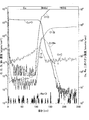
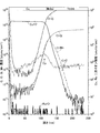
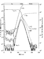
- Structure diagram of produced samples 1A and 1B (1) Correlation diagram between Ru film formation time and Ru film thickness Correlation diagram of Ru film thickness and sheet resistance Structure diagram of the produced samples 2A, 2B, 3A and 3B (2) Structure diagram of produced samples 4A and 4B (3) Correlation diagram of depth and concentration obtained by SIMS analysis of the prepared sample 2A Correlation diagram of depth and concentration obtained by SIMS analysis of sample 2B Correlation diagram between depth and concentration obtained by SIMS analysis of sample 3A Correlation diagram between depth and concentration obtained by SIMS analysis of sample 3B Correlation diagram of depth and concentration obtained by SIMS analysis of the prepared sample 4A Correlation diagram of depth and concentration obtained by SIMS analysis of sample 4B Configuration diagram of a semiconductor device manufacturing apparatus in the present embodiment Configuration diagram of another semiconductor device manufacturing apparatus in the present embodiment Explanatory drawing of the manufacturing method of the semiconductor device in this Embodiment Process drawing (1) of the manufacturing method of the semiconductor device in this Embodiment Process drawing (2) of the manufacturing method of the semiconductor device in this Embodiment TEM images of the
- manganese oxide includes MnO, Mn 3 O 4 , Mn 2 O 3 , MnO 2, and the like depending on the valence, and these are all represented by MnOx.
- X is a value of 1 or more and 2 or less.
- MnSixOy manganese silicate
- a substrate in which a TEOS film 10 b is formed on a silicon substrate 10 a is used.
- an argon atmosphere The substrate was degassed by heating to about 250 ° C.
- the Ru film 12 was formed by CVD under the condition of the substrate temperature of about 200 ° C.
- Sample 1B was heated to 400 ° C. and subjected to hydrogen radical treatment, and then the Ru film 12 was formed by CVD under a substrate temperature of about 200 ° C.
- an organic metal material such as (EtCp) 2 Mn is used as a film forming material
- an organometallic material such as Ru 3 (CO) 12 is used as a film forming material.
- the hydrogen radical treatment means a treatment in which atomic hydrogen is generated by remote plasma, plasma, a heating filament or the like and a predetermined surface of the substrate 10 is irradiated with the generated atomic hydrogen.
- FIG. 2 shows the relationship between the film formation time and film thickness of the Ru film in Sample 1A and Sample 1B.
- Sample 1A when the Ru film 12 is formed on the MnOx film 11 without subjecting the MnOx film 11 to hydrogen radical treatment, the Ru film may not be deposited until 10 seconds have elapsed. It is assumed that the incubation time is about 10 seconds.
- FIG. 3 shows the relationship between the film thickness of the Ru film 12 and the sheet resistance Rs in the samples 1A and 1B.
- a case where an SiO 2 film, a Ti film, and a TaN film are formed in place of the MnOx film 11 is also shown.
- the sheet resistance Rs is high as in the case where the base is the SiO 2 film, The film resistance dependency of the sheet resistance Rs on the Ru film 12 is also high.
- the deposition rate of the Ru film 12 can be increased, the incubation time for forming the Ru film can be shortened, and the sheet resistance Rs can be decreased.
- the uniformity of the Ru film thickness in the wafer surface can be improved. This is presumably because the MnOx on the surface of the MnOx film 11 was reduced to Mn by performing hydrogen radical treatment.
- Other possibilities include a decrease in x of MnOx, a change in MnOx to MnSixOy, a hydrogen termination of the surface of MnOx, a reduction in residual carbon in the MnOx film, These combined effects can be considered.
- each sample is formed so that the TEOS film 10b is 100 nm, the MnOx film 11 is 4.5 nm, the Ru film 12 is 2 nm, and the Cu film 13 is 100 nm.
- Samples 2B, 3B, and 4B were annealed at 400 ° C. for 1 hour in an argon atmosphere after film formation.
- FIG. 6 shows the SIMS analysis result of sample 2A
- FIG. 7 shows the analysis result of sample 2B by SIMS
- FIG. 8 shows the analysis result of sample 3A by SIMS
- FIG. 9 shows the analysis result of sample 3B by SIMS
- FIG. 10 shows the SIMS analysis result of sample 4A
- FIG. 11 shows the SIMS analysis result of sample 4B.
- the analysis results by SIMS in FIGS. 6 to 11 show the film depth on the horizontal axis and the concentration of each element on the vertical axis.
- the film formation rate of the Ru film 12 can be increased by performing the hydrogen radical treatment after the MnOx film 11 is formed. Resistance can also be lowered. Moreover, a part of C component in a film
- membrane can be removed by performing a hydrogen radical process.
- the present invention is based on the knowledge obtained as a result of the above examination.
- FIG. 12 shows a processing system which is a semiconductor device manufacturing apparatus in the present embodiment.
- This processing system has four processing apparatuses 111, 112, 113, 114, a substantially hexagonal common transfer chamber 121, a first load lock chamber 122 and a second load lock chamber 123 having a load lock function, and an elongated introduction.
- a side transfer chamber 124 is provided.
- Gate valves G are respectively provided between the four processing apparatuses 111 to 114 and the substantially hexagonal common transfer chamber 121, and the transfer chamber 121, the first load lock chamber 122, and the second load lock chamber 123 are connected to each other.
- a gate valve G is provided between the first load lock chamber 122 and the second load lock chamber 123, and the introduction-side transfer chamber 124, respectively.
- Each gate valve G can be opened and closed.
- the wafer W can be moved between apparatuses.
- three introduction ports 125 are connected to the introduction-side transfer chamber 124 via an opening / closing door 126, and a cassette container 127 in which a plurality of wafers W are stored is accommodated in the introduction port 125.
- an orienter 128 is provided in the introduction-side transfer chamber 124, and the wafer W is positioned.
- a transfer mechanism 131 having a pickup that can bend and stretch in order to transfer the wafer W is provided in the transfer chamber 121.
- the introduction-side transfer chamber 124 is provided with an introduction-side transfer mechanism 132 having a pickup that can bend and stretch to transfer the wafer W.
- the introduction-side transfer mechanism 132 is provided in the introduction-side transfer chamber 124. It is supported in a slidable state on the provided guide rail 133.
- the wafer W is, for example, a silicon wafer or the like, and is stored in the cassette container 127.
- the wafer W is transferred from the introduction port 125 to the first load lock chamber 122 or the second load lock chamber 123 by the introduction side transfer mechanism 132 and transferred to the first load lock chamber 122 or the second load lock chamber 123.
- W is transferred to the four processing apparatuses 111 to 114 by the transfer mechanism 131 provided in the common transfer chamber 121.
- the wafer W is also transferred by the transfer mechanism 131 when the wafer W is moved between the four processing apparatuses 111 to 114. By moving between the processing apparatuses 111 to 114 in this way, the processing on the wafer W is performed in each of the processing apparatuses 111 to 114.
- Such control of the transfer and processing of the wafer W is performed by the system control unit 134, and a program for performing the system control is stored in the storage medium 136.
- the first processing apparatus 111 is for forming a MnOx film
- the second processing apparatus 112 is MnOx by atomic hydrogen or the like.
- the third processing unit 113 is for forming a Ru film
- the fourth processing unit 114 is for forming a Cu film.
- a remote plasma generator 120 for generating atomic hydrogen is connected to the second processing apparatus 112, and hydrogen radical processing is performed by irradiating the generated atomic hydrogen onto the wafer W.
- a plasma generation unit may be provided inside the second processing apparatus 112, or a heating filament is provided for heating.
- the structure of generating atomic hydrogen may be used.
- the processing performed in the first processing device 111, the second processing device 112, and the third processing device 113 can be performed by one processing device 116.
- the processing apparatus 116 to which the remote plasma generation unit 120 is connected is connected to the common transfer chamber 121 via the gate valve G.
- a processing apparatus 117 for performing pretreatment (for example, degassing) of the wafer W may be provided as shown in FIG.
- the method for manufacturing a semiconductor device in the present embodiment is a method for manufacturing a semiconductor device having a multilayer wiring structure, and is for wiring between layers. Therefore, the formed semiconductor element and the method for forming the semiconductor element are omitted.
- an insulating film to be an interlayer insulating film is formed.
- an insulating layer 211 is formed on a substrate 210 such as a silicon substrate, and a wiring layer 212 made of copper or the like is formed on the surface of the insulating film 211.
- an insulating film 213 made of SiO 2 or the like to be an interlayer insulating film is formed.
- the wiring layer 212 is connected to a transistor (not shown) formed on the surface of the substrate 210 and other wiring.
- step 104 an opening is formed in the insulating film 213.
- a predetermined region of the insulating film 213 is removed by etching or the like until the surface of the wiring layer 212 is exposed, and an opening 214 is formed.
- the opening 214 is composed of an elongated groove (trench) 214a and a hole 214b formed in a part of the bottom of the groove 214a.
- the wiring layer 212 is formed. Is exposed.
- Such an opening 214 may be formed by, for example, applying a photoresist on the surface of the insulating film 213, exposing by an exposure apparatus, RIE (Reactive It can be formed by repeating an etching process such as Ion Etching.
- step 106 a degas process or a cleaning process is performed as a pre-process. Thereby, the inside of the opening 214 is cleaned.
- cleaning treatment include H 2 annealing treatment, H 2 plasma treatment, Ar plasma treatment, and dry cleaning treatment using an organic acid.
- step 108 a film containing Mn such as a MnOx film to be the first film is formed (first film forming process).
- first film forming process a film containing Mn such as a MnOx film to be the first film is formed.
- the substrate 210 is heated to 200 ° C., and an MnOx film 215 is formed by CVD using an organometallic raw material containing Mn.
- the MnOx film 215 is formed on the side surface of the opening 214 except the bottom of the hole 214b.
- the MnOx film 215 may be formed with a MnSixOy film at the boundary with the insulating film 213.
- the MnOx film 215 is almost entirely formed on the surface of the wiring layer 212 due to the selective growth of CVD. Are not deposited, and are mainly formed on the side surface of the opening 214 or the like.
- the film thickness of the MnOx film 215 to be formed is 0.5 to 5 nm.
- the MnOx film 215 is formed by ALD (Atomic) in addition to the CVD method. You may carry out by the Layer Deposition) method. In this embodiment, the case where the MnOx film 215 is used as the first film will be described.
- a metal oxide can be given, and more preferably Mg, 1 selected from Al, Ca, Ti, V, Cr, Mn, Fe, Co, Ni, Ge, Sr, Y, Zr, Nb, Mo, Rh, Pd, Sn, Ba, Hf, Ta and Ir
- Mg, 1 selected from Al, Ca, Ti, V, Cr, Mn, Fe, Co, Ni, Ge, Sr, Y, Zr, Nb, Mo, Rh, Pd, Sn, Ba, Hf, Ta and Ir
- step 110 hydrogen radical treatment step.
- atomic hydrogen is generated by remote plasma, plasma, a heating filament, or the like, and the generated atomic hydrogen is irradiated on the surface of the MnOx layer 215.
- atomic hydrogen is generated by the remote plasma generated in the remote plasma generator 120 shown in FIGS. 12 and 13 and the like, and the generated atomic hydrogen is formed into a film of MnOx 215 on the substrate 210. Irradiate the surface.
- heat treatment is preferably performed together.
- the substrate 210 is heated to 400 ° C. This temperature is higher than the deposition temperature of the MnOx film 215 and the deposition temperature of the Ru film 216 described later.
- the hydrogen radical treatment is performed for 60 seconds in a gas atmosphere of H 2 : 10% and Ar: 90% at a treatment pressure of 40 Pa, an input power of 3 kW, and a substrate heating temperature of 400 ° C.
- the heating temperature of the substrate 210 is preferably room temperature to 450 ° C., more preferably 200 ° C. to 400 ° C., and further preferably 400 ° C.
- the H 2 concentration in Ar is preferably 1 to 20%, more preferably 5 to 15%, and further preferably H 2 : 10% and Ar: 90%.
- the processing pressure is preferably 10 to 500 Pa, more preferably 20 to 100 Pa, and further preferably 40 Pa.
- the input power is preferably 1 to 5 kW, more preferably 2 to 4 kW, and further preferably 3 kW.
- the treatment time is preferably 5 to 300 seconds, more preferably 10 to 100 seconds, and further preferably 60 seconds.
- a degas process heat treatment process
- a Ru film to be the second film is formed (second film forming process).
- a Ru film 216 is formed by CVD by heating the substrate 210 to about 200 ° C. using an organometallic material containing Ru.
- the Ru film 216 is a metal material and is formed on the inner surface of the opening 214 including the bottom surface of the hole 214b. That is, the Ru film 216 is formed on the surface of the wiring layer 212 and the MnOx layer 215 exposed in the opening 214. Since the MnOx layer 215 is not formed on the exposed surface of the wiring layer 212 as described above at the bottom surface of the hole 214b, the Ru film 216 is formed on the surface of the wiring layer 212.
- the hydrogen radical treatment in step 110 and the Ru film 216 in step 112 are performed in the same chamber as shown in FIG. 13, or the hydrogen radical treatment as shown in FIG.
- the chamber for forming the Ru film 216 and the chamber for forming the Ru film 216 are connected by a common transfer chamber 121 capable of maintaining a predetermined degree of vacuum, and the wafer W can be moved through the common transfer chamber 121. It is preferable.
- a cooling process may be provided between the hydrogen radical treatment in step 110 and the formation of the Ru film 216 in step 112 to cool the substrate 210 to a temperature lower than the Ru film formation temperature, for example, room temperature.
- the film thickness of the Ru film 216 to be formed is 0.5 to 5 nm, and the Ru film 216 may be formed by the ALD method in addition to the CVD method. In this embodiment, the case where the Ru film 216 is used as the second film will be described.
- Fe, Co, Ni, Ru, Rh, Pd, Os , Ir and Pt, or one or more elements selected from Pt may be included. Furthermore, it may contain one or more elements selected from platinum group elements.
- a Cu film is formed (electrode formation step).
- the Cu film 217 is formed by any one of the CVD method, ALD method, PVD method, electrolytic plating method, electroless plating method, and supercritical CO 2 method.
- the method for forming the Cu film 217 may be a combination of the above methods.
- a Cu film 217 is formed by first depositing a thin Cu film by sputtering and then depositing Cu by electrolytic plating.
- planarization is performed by CMP (Chemical Mechanical Polishing) or the like as necessary.
- CMP Chemical Mechanical Polishing
- the MnOx film 215 in step 108, the hydrogen radical treatment in step 110, and the Ru film 216 in step 112 may be performed in the same chamber (processing apparatus), or may be performed in different chambers (processing apparatuses). You may go.
- the manufacturing method of the present invention it is possible to miniaturize the Cu multilayer wiring. As an effect obtained by this, it is possible to make a small and high-speed and reliable electronic device by increasing the speed and miniaturization of a semiconductor device (device).
- Sample 17B was manufactured by performing hydrogen annealing instead of hydrogen radical processing, that is, by sequentially performing insulating film deposition, MnO film deposition, hydrogen annealing treatment, and Ru film deposition. is there.
- Sample 17C was fabricated without performing hydrogen radical treatment and hydrogen annealing treatment, that is, fabricated by sequentially performing insulating film deposition, MnO film deposition, and Ru film deposition. The hydrogen radical treatment in sample 17A and the hydrogen annealing treatment in sample 17B are performed at substantially the same temperature.
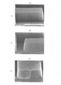
- FIG. 17 shows TEM images of samples 17A, 17B, and 17C
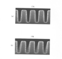
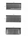
- FIGS. 18 to 21 show SEM images of samples 17A, 17B, and 17C
- 17A is a TEM image of sample 17A
- FIG. 17B is a TEM image of sample 17B
- FIG. 17C is a TEM image of sample 17C
- 18 to 21 are SEM images at different angles
- FIGS. 18 (a) to 21 (a) are SEM images of the sample 17A
- FIGS. 18 (b) to 21 (b) are FIG. 18C
- FIG. 21C are SEM images of the sample 17C.
- the sample shown in FIG. 17 and the sample formed in FIGS. 18 to 21 are formed on different substrates.
- FIGS. 20 and 21 are SEM images in different regions.
- the Ru film is thicker and smoother than the samples 17B and 17C.
- the incubation time is shortened in the sample 17A because the Ru film is formed thicker than the samples 17B and 17C.
- the sample 17A has less unevenness on the surface than the samples 17B and 17C, and is formed smoothly.
- the hydrogen radical treatment is significantly better than the case where the hydrogen radical treatment is not performed or the case where the hydrogen annealing treatment is performed instead of the hydrogen radical treatment. Can be obtained.
Landscapes
- Electrodes Of Semiconductors (AREA)
- Chemical Vapour Deposition (AREA)
- Internal Circuitry In Semiconductor Integrated Circuit Devices (AREA)
Abstract
Description
最初に、本発明に至るまでの検討内容について説明する。具体的には、図1に示すように、基板10上に第1の膜となるMnOx膜11及び第2の膜となるRu膜12を積層形成したものについて、MnOx膜11における水素ラジカル処理の有無の違いによるRu膜12の成膜レート及びシート抵抗について説明する。
次に、図4に示すように、基板10に成膜されたMnOx膜11上にCu膜13を形成したもの(サンプル2A、2B、3A、3B)及び、図5に示すように基板10に成膜されたMnOx膜11上にRu膜12を成膜し、更にCu膜13を成膜したもの(サンプル4A、4B)におけるSIMS(Secondary Ion-microprobe Mass Spectrometer)による組成分析を行なった結果について説明する。
本実施の形態における半導体装置の製造装置について説明する。尚、ウエハWとは、基板または膜が成膜された基板を意味するものである。図12は、本実施の形態における半導体装置の製造装置である処理システムを示すものである。この処理システムは、4つの処理装置111、112、113、114と、略六角形状の共通搬送室121と、ロードロック機能を有する第1ロードロック室122及び第2ロードロック室123と、細長い導入側搬送室124を有している。4つの処理装置111~114と略六角形状の共通搬送室121との間には各々ゲートバルブGが設けられており、搬送室121と第1ロードロック室122及び第2ロードロック室123との間には各々ゲートバルブGが設けられており、第1ロードロック室122及び第2ロードロック室123と導入側搬送室124との間には各々ゲートバルブGが設けられている。各々のゲートバルブGは開閉可能であり、ゲートバルブGが開くことにより装置間等においてウエハWを移動させることができる。導入側搬送室124には、例えば、3つの導入ポート125が開閉ドア126を介し接続されており、導入ポート125には複数のウエハWが収納されたカセット容器127が納められている。また、導入側搬送室124には、オリエンタ128が設けられており、ウエハWの位置決め等がなされる。
次に、図14に基づき本実施の形態における半導体装置の製造方法について説明する。本実施の形態における半導体装置の製造方法は、多層配線構造を有する半導体装置の製造方法であって、層間の配線を行なうためのものである。よって、形成されている半導体素子及び半導体素子の形成方法については省略されている。
Ion Etching)等によるエッチングの工程を繰り返すことにより形成することができる。
Layer Deposition)法により行ってもよい。また、本実施の形態においては、第1の膜としてMnOx膜215を用いた場合について説明するが、第1の膜を形成する材料としては、金属酸化物が挙げられ、より好ましくは、Mg、Al、Ca、Ti、V、Cr、Mn、Fe、Co、Ni、Ge、Sr、Y、Zr、Nb、Mo、Rh、Pd、Sn、Ba、Hf、Ta及びIrのうちから選ばれる1または2以上の元素の酸化物を含むものが挙げられる。
次に、実際にRu膜を作製したものについて、TEM(Transmission Electron Microscope)像の観察及びSEM(Scanning Electron Microscope)像の観察を行なった結果について説明する。具体的には、Ru膜が形成されている3種類のサンプル、即ち、サンプル17A、17B、17Cを作製し、TEM像の観察及びSEM像の観察を行なった。サンプル17Aは、図14に示される本実施の形態における製造方法の一部と同様の方法、即ち、絶縁膜成膜、MnO膜成膜、水素ラジカル処理、Ru膜成膜を順に行なうことにより作製したものである。サンプル17Bは、水素ラジカル処理に代えて水素アニール処理を行なうことにより作製したもの、即ち、絶縁膜成膜、MnO膜成膜、水素アニール処理、Ru膜成膜を順に行なうことにより作製したものである。サンプル17Cは、水素ラジカル処理及び水素アニール処理を行なうことなく作製したもの、即ち、絶縁膜成膜、MnO膜成膜、Ru膜成膜を順に行なうことにより作製したものである。尚、サンプル17Aにおける水素ラジカル処理とサンプル17Bにおける水素アニール処理とは、略同じ温度により行なっている。
10a シリコン基板
10b TEOS膜
11 MnOx膜(第1の膜)
12 Ru膜(第2の膜)
13 Cu膜
111 第1の処理装置
112 第2の処理装置
113 第3の処理装置
114 第4の処理装置
120 リモートプラズマ発生部
121 共通搬送室
122 第1ロードロック室
123 第2ロードロック室
124 導入側搬送室
125 導入ポート
126 開閉ドア
127 カセット容器
128 オリエンタ
131 搬送機構
132 導入側搬送機構
133 案内レール
210 基板
211 絶縁層
212 配線層
213 絶縁膜
214 開口部
214a 溝
214b ホール
215 MnOx膜
216 Ru膜
217 Cu膜
Claims (19)
- 基板表面に絶縁膜が形成されており、前記絶縁膜に形成された開口部の内部に金属酸化物からなる第1の膜を成膜する第1の成膜工程と、
前記第1の膜に原子状水素を照射する水素ラジカル処理工程と、
前記水素ラジカル処理工程の後、前記開口部の内部に金属からなる第2の膜を成膜する第2の成膜工程と、
前記第2の膜を成膜した後、前記開口部の内部に金属からなる電極を形成する電極形成工程と、
を有することを特徴とする半導体装置の製造方法。 - 前記水素ラジカル処理工程は、前記第2の膜におけるインキュベーション時間の短縮、膜厚均一性、シート抵抗、密着性のいずれかを向上させるものであることを特徴とする請求項1に記載の半導体装置の製造方法。
- 前記水素ラジカル処理は、前記基板を加熱した状態で行なわれることを特徴とする請求項1または2に記載の半導体装置の製造方法。
- 前記水素ラジカル処理は前記第1の膜中のC成分を減らすことを特徴とする請求項1から3のいずれかに記載の半導体装置の製造方法。
- 前記原子状水素はリモートプラズマにより発生されたものであることを特徴とする請求項1から4のいずれかに記載の半導体装置の製造方法。
- 前記第1の膜は、Mg、Al、Ca、Ti、V、Cr、Mn、Fe、Co、Ni、Ge、Sr、Y、Zr、Nb、Mo、Rh、Pd、Sn、Ba、Hf、Ta及びIrのうちから選ばれる1または2以上の元素の酸化物を含むものにより形成されているものであることを特徴とする請求項1から5のいずれかに記載の半導体装置の製造方法。
- 前記第1の膜は、Mnの酸化物を含むものであることを特徴とする請求項1から6のいずれかに記載の半導体装置の製造方法。
- 前記第1の膜は、CVD法、ALD法または超臨界CO2法により成膜されたものであることを特徴とする請求項1から7のいずれかに記載の半導体装置の製造方法。
- 前記第1の膜は、熱CVD法または熱ALD法またはプラズマCVD法またはプラズマALD法または超臨界CO2法により成膜されたものであることを特徴とする請求項1から7のいずれかに記載の半導体装置の製造方法。
- 前記第2の膜は、Fe、Co、Ni、Ru、Rh、Pd、Os、Ir及びPtのうちから選ばれる1または2以上の元素を含むものにより形成されていることを特徴とする請求項1から9のいずれかに記載の半導体装置の製造方法。
- 前記第2の膜は、CVD法、ALD法または超臨界CO2法により成膜されたものであることを特徴とする請求項1から10のいずれかに記載の半導体装置の製造方法。
- 前記第2の膜は、熱CVD法または熱ALD法またはプラズマCVD法またはプラズマALD法または超臨界CO2法により成膜されたものであることを特徴とする請求項1から10のいずれかに記載の半導体装置の製造方法。
- 前記電極は、銅または銅を含む材料により形成されていることを特徴とする請求項1から12のいずれかに記載の半導体装置の製造方法。
- 前記電極は、熱CVD法、熱ALD法、プラズマCVD法、プラズマALD法、PVD法、電解メッキ法、無電解メッキ法、超臨界CO2法から選ばれる1または2以上の方法により成膜されたものであることを特徴とする請求項1から13のいずれかに記載の半導体装置の製造方法。
- 請求項1から14のいずれかに記載の半導体装置の製造方法によって形成された膜構造を有することを特徴とする半導体装置。
- 基板表面に絶縁膜が形成されており、前記絶縁膜に形成された開口部の内部に金属酸化物からなる第1の膜を成膜し、前記第1の膜に原子状水素を照射し、前記原子状水素を照射した後、前記開口部の内部に金属からなる第2の膜を成膜し、前記第2の膜上に金属からなる電極を形成する半導体装置の製造装置において、
第1の膜に原子状水素を照射することを特徴とする半導体装置の製造装置。 - 前記原子状水素を発生させるためリモートプラズマ発生部を有することを特徴とする請求項16に記載の半導体装置の製造装置。
- 前記基板を加熱するための加熱手段を有することを特徴とする請求項16または17に記載の半導体装置の製造装置。
- 請求項1から14のいずれかに記載の製造方法を実施するように制御するシステム制御部(コンピュータ)に読み取り可能なプログラムを記憶することを特徴とする記憶媒体。
Priority Applications (2)
| Application Number | Priority Date | Filing Date | Title |
|---|---|---|---|
| KR1020147001078A KR101659469B1 (ko) | 2011-06-16 | 2012-06-08 | 반도체 장치의 제조 방법, 반도체 장치, 반도체 장치의 제조 장치 및 기억 매체 |
| US14/105,514 US20140103529A1 (en) | 2011-06-16 | 2013-12-13 | Semiconductor device manufacturing method, semiconductor device, semiconductor device manufacturing apparatus and storage medium |
Applications Claiming Priority (2)
| Application Number | Priority Date | Filing Date | Title |
|---|---|---|---|
| JP2011134317 | 2011-06-16 | ||
| JP2011-134317 | 2011-06-16 |
Related Child Applications (1)
| Application Number | Title | Priority Date | Filing Date |
|---|---|---|---|
| US14/105,514 Continuation US20140103529A1 (en) | 2011-06-16 | 2013-12-13 | Semiconductor device manufacturing method, semiconductor device, semiconductor device manufacturing apparatus and storage medium |
Publications (1)
| Publication Number | Publication Date |
|---|---|
| WO2012173067A1 true WO2012173067A1 (ja) | 2012-12-20 |
Family
ID=47357056
Family Applications (1)
| Application Number | Title | Priority Date | Filing Date |
|---|---|---|---|
| PCT/JP2012/064844 Ceased WO2012173067A1 (ja) | 2011-06-16 | 2012-06-08 | 半導体装置の製造方法、半導体装置、半導体装置の製造装置及び記憶媒体 |
Country Status (5)
| Country | Link |
|---|---|
| US (1) | US20140103529A1 (ja) |
| JP (1) | JPWO2012173067A1 (ja) |
| KR (1) | KR101659469B1 (ja) |
| TW (1) | TWI470679B (ja) |
| WO (1) | WO2012173067A1 (ja) |
Cited By (9)
| Publication number | Priority date | Publication date | Assignee | Title |
|---|---|---|---|---|
| WO2014013941A1 (ja) * | 2012-07-18 | 2014-01-23 | 東京エレクトロン株式会社 | 半導体装置の製造方法 |
| JP2015177119A (ja) * | 2014-03-17 | 2015-10-05 | 東京エレクトロン株式会社 | Cu配線の製造方法 |
| KR20160111333A (ko) | 2015-03-16 | 2016-09-26 | 도쿄엘렉트론가부시키가이샤 | 구리 배선의 제조 방법 |
| KR20170026165A (ko) | 2015-08-31 | 2017-03-08 | 도쿄엘렉트론가부시키가이샤 | 반도체 장치의 제조 방법 및 기억 매체 |
| JP2017092101A (ja) * | 2015-11-04 | 2017-05-25 | 東京エレクトロン株式会社 | パターン形成方法 |
| US9892965B2 (en) | 2016-01-27 | 2018-02-13 | Tokyo Electron Limited | Cu wiring manufacturing method and Cu wiring manufacturing system |
| US10096548B2 (en) | 2015-03-16 | 2018-10-09 | Tokyo Electron Limited | Method of manufacturing Cu wiring |
| TWI720422B (zh) * | 2013-09-27 | 2021-03-01 | 美商應用材料股份有限公司 | 實現無縫鈷間隙填充之方法 |
| JP2024061924A (ja) * | 2022-10-24 | 2024-05-09 | 嶺南大學校 産學協力團 | バリア層及びバリア層の形成方法並びに配線基板 |
Families Citing this family (2)
| Publication number | Priority date | Publication date | Assignee | Title |
|---|---|---|---|---|
| JP5353109B2 (ja) * | 2008-08-15 | 2013-11-27 | 富士通セミコンダクター株式会社 | 半導体装置の製造方法 |
| KR102238257B1 (ko) * | 2014-08-26 | 2021-04-13 | 삼성전자주식회사 | 반도체 소자의 제조 방법 |
Citations (5)
| Publication number | Priority date | Publication date | Assignee | Title |
|---|---|---|---|---|
| JP2006128541A (ja) * | 2004-11-01 | 2006-05-18 | Nec Electronics Corp | 電子デバイスの製造方法 |
| JP2008124275A (ja) * | 2006-11-13 | 2008-05-29 | Fujitsu Ltd | 半導体装置の製造方法 |
| JP2009147137A (ja) * | 2007-12-14 | 2009-07-02 | Toshiba Corp | 半導体装置およびその製造方法 |
| JP2010021447A (ja) * | 2008-07-11 | 2010-01-28 | Tokyo Electron Ltd | 成膜方法及び処理システム |
| JP2010040771A (ja) * | 2008-08-05 | 2010-02-18 | Rohm Co Ltd | 半導体装置の製造方法 |
Family Cites Families (5)
| Publication number | Priority date | Publication date | Assignee | Title |
|---|---|---|---|---|
| JP2008300568A (ja) | 2007-05-30 | 2008-12-11 | Tokyo Electron Ltd | 半導体装置の製造方法、半導体製造装置及び記憶媒体 |
| US8110504B2 (en) * | 2008-08-05 | 2012-02-07 | Rohm Co., Ltd. | Method of manufacturing semiconductor device |
| JP4415100B1 (ja) | 2008-12-19 | 2010-02-17 | 国立大学法人東北大学 | 銅配線、半導体装置および銅配線形成方法 |
| US8425987B2 (en) * | 2008-12-31 | 2013-04-23 | Intel Corporation | Surface charge enhanced atomic layer deposition of pure metallic films |
| US20110204518A1 (en) * | 2010-02-23 | 2011-08-25 | Globalfoundries Inc. | Scalability with reduced contact resistance |
-
2012
- 2012-06-08 KR KR1020147001078A patent/KR101659469B1/ko not_active Expired - Fee Related
- 2012-06-08 JP JP2013520532A patent/JPWO2012173067A1/ja not_active Ceased
- 2012-06-08 WO PCT/JP2012/064844 patent/WO2012173067A1/ja not_active Ceased
- 2012-06-15 TW TW101121446A patent/TWI470679B/zh not_active IP Right Cessation
-
2013
- 2013-12-13 US US14/105,514 patent/US20140103529A1/en not_active Abandoned
Patent Citations (5)
| Publication number | Priority date | Publication date | Assignee | Title |
|---|---|---|---|---|
| JP2006128541A (ja) * | 2004-11-01 | 2006-05-18 | Nec Electronics Corp | 電子デバイスの製造方法 |
| JP2008124275A (ja) * | 2006-11-13 | 2008-05-29 | Fujitsu Ltd | 半導体装置の製造方法 |
| JP2009147137A (ja) * | 2007-12-14 | 2009-07-02 | Toshiba Corp | 半導体装置およびその製造方法 |
| JP2010021447A (ja) * | 2008-07-11 | 2010-01-28 | Tokyo Electron Ltd | 成膜方法及び処理システム |
| JP2010040771A (ja) * | 2008-08-05 | 2010-02-18 | Rohm Co Ltd | 半導体装置の製造方法 |
Cited By (15)
| Publication number | Priority date | Publication date | Assignee | Title |
|---|---|---|---|---|
| WO2014013941A1 (ja) * | 2012-07-18 | 2014-01-23 | 東京エレクトロン株式会社 | 半導体装置の製造方法 |
| TWI720422B (zh) * | 2013-09-27 | 2021-03-01 | 美商應用材料股份有限公司 | 實現無縫鈷間隙填充之方法 |
| KR101846049B1 (ko) * | 2014-03-17 | 2018-04-05 | 도쿄엘렉트론가부시키가이샤 | Cu 배선의 제조 방법 및 기억 매체 |
| JP2015177119A (ja) * | 2014-03-17 | 2015-10-05 | 東京エレクトロン株式会社 | Cu配線の製造方法 |
| US9362166B2 (en) | 2014-03-17 | 2016-06-07 | Tokyo Electron Limited | Method of forming copper wiring |
| TWI710654B (zh) * | 2014-03-17 | 2020-11-21 | 日商東京威力科創股份有限公司 | Cu配線之製造方法 |
| KR20160111333A (ko) | 2015-03-16 | 2016-09-26 | 도쿄엘렉트론가부시키가이샤 | 구리 배선의 제조 방법 |
| KR20180068328A (ko) | 2015-03-16 | 2018-06-21 | 도쿄엘렉트론가부시키가이샤 | 구리 배선의 제조 방법 |
| US10096548B2 (en) | 2015-03-16 | 2018-10-09 | Tokyo Electron Limited | Method of manufacturing Cu wiring |
| JP2016174141A (ja) * | 2015-03-16 | 2016-09-29 | 東京エレクトロン株式会社 | Cu配線の製造方法 |
| US9735046B2 (en) | 2015-08-31 | 2017-08-15 | Tokyo Electron Limited | Semiconductor device manufacturing method and storage medium |
| KR20170026165A (ko) | 2015-08-31 | 2017-03-08 | 도쿄엘렉트론가부시키가이샤 | 반도체 장치의 제조 방법 및 기억 매체 |
| JP2017092101A (ja) * | 2015-11-04 | 2017-05-25 | 東京エレクトロン株式会社 | パターン形成方法 |
| US9892965B2 (en) | 2016-01-27 | 2018-02-13 | Tokyo Electron Limited | Cu wiring manufacturing method and Cu wiring manufacturing system |
| JP2024061924A (ja) * | 2022-10-24 | 2024-05-09 | 嶺南大學校 産學協力團 | バリア層及びバリア層の形成方法並びに配線基板 |
Also Published As
| Publication number | Publication date |
|---|---|
| KR101659469B1 (ko) | 2016-09-23 |
| TW201322312A (zh) | 2013-06-01 |
| US20140103529A1 (en) | 2014-04-17 |
| KR20140041745A (ko) | 2014-04-04 |
| JPWO2012173067A1 (ja) | 2015-02-23 |
| TWI470679B (zh) | 2015-01-21 |
Similar Documents
| Publication | Publication Date | Title |
|---|---|---|
| WO2012173067A1 (ja) | 半導体装置の製造方法、半導体装置、半導体装置の製造装置及び記憶媒体 | |
| CN100477158C (zh) | 半导体器件的制造方法以及半导体器件 | |
| KR101692170B1 (ko) | 반도체 장치의 제조 방법 | |
| KR101532814B1 (ko) | 루테늄 금속캡층을 형성하는 반도체 디바이스 형성 방법 | |
| CN101715602B (zh) | 成膜方法和成膜装置 | |
| JP6360276B2 (ja) | 半導体装置、半導体装置の製造方法、半導体製造装置 | |
| JP5522979B2 (ja) | 成膜方法及び処理システム | |
| TW201138024A (en) | Interfacial layers for electromigration resistance improvement in damascene interconnects | |
| US9153481B2 (en) | Manganese-containing film forming method, processing system, electronic device manufacturing method and electronic device | |
| CN101689490B (zh) | 成膜方法和处理系统 | |
| WO2001013415A1 (fr) | Procede de fabrication d'un dispositif a semi-conducteurs et fabrication dudit dispositif | |
| van der Straten et al. | Atomic Layer Deposition of Tantalum Nitride on Organosilicate and Organic Polymer-based Low Dielectric Constant Materials | |
| KR100872799B1 (ko) | 플라스마 원자층 증착법을 이용한 반도체 콘택트용 금속실리사이드 제조방법 | |
| JP3639142B2 (ja) | 半導体装置の製造方法 |
Legal Events
| Date | Code | Title | Description |
|---|---|---|---|
| 121 | Ep: the epo has been informed by wipo that ep was designated in this application |
Ref document number: 12801204 Country of ref document: EP Kind code of ref document: A1 |
|
| ENP | Entry into the national phase |
Ref document number: 2013520532 Country of ref document: JP Kind code of ref document: A |
|
| NENP | Non-entry into the national phase |
Ref country code: DE |
|
| ENP | Entry into the national phase |
Ref document number: 20147001078 Country of ref document: KR Kind code of ref document: A |
|
| 122 | Ep: pct application non-entry in european phase |
Ref document number: 12801204 Country of ref document: EP Kind code of ref document: A1 |