WO2012169269A1 - 安定性判定方法、安定性判定回路、電力変換装置 - Google Patents
安定性判定方法、安定性判定回路、電力変換装置 Download PDFInfo
- Publication number
- WO2012169269A1 WO2012169269A1 PCT/JP2012/058958 JP2012058958W WO2012169269A1 WO 2012169269 A1 WO2012169269 A1 WO 2012169269A1 JP 2012058958 W JP2012058958 W JP 2012058958W WO 2012169269 A1 WO2012169269 A1 WO 2012169269A1
- Authority
- WO
- WIPO (PCT)
- Prior art keywords
- value
- stability determination
- converter
- inverter
- power
- Prior art date
- Legal status (The legal status is an assumption and is not a legal conclusion. Google has not performed a legal analysis and makes no representation as to the accuracy of the status listed.)
- Ceased
Links
Images






Classifications
-
- H—ELECTRICITY
- H02—GENERATION; CONVERSION OR DISTRIBUTION OF ELECTRIC POWER
- H02M—APPARATUS FOR CONVERSION BETWEEN AC AND AC, BETWEEN AC AND DC, OR BETWEEN DC AND DC, AND FOR USE WITH MAINS OR SIMILAR POWER SUPPLY SYSTEMS; CONVERSION OF DC OR AC INPUT POWER INTO SURGE OUTPUT POWER; CONTROL OR REGULATION THEREOF
- H02M5/00—Conversion of AC power input into AC power output, e.g. for change of voltage, for change of frequency, for change of number of phases
- H02M5/40—Conversion of AC power input into AC power output, e.g. for change of voltage, for change of frequency, for change of number of phases with intermediate conversion into DC
- H02M5/42—Conversion of AC power input into AC power output, e.g. for change of voltage, for change of frequency, for change of number of phases with intermediate conversion into DC by static converters
- H02M5/44—Conversion of AC power input into AC power output, e.g. for change of voltage, for change of frequency, for change of number of phases with intermediate conversion into DC by static converters using discharge tubes or semiconductor devices to convert the intermediate DC into AC
- H02M5/453—Conversion of AC power input into AC power output, e.g. for change of voltage, for change of frequency, for change of number of phases with intermediate conversion into DC by static converters using discharge tubes or semiconductor devices to convert the intermediate DC into AC using devices of a triode or transistor type requiring continuous application of a control signal
- H02M5/458—Conversion of AC power input into AC power output, e.g. for change of voltage, for change of frequency, for change of number of phases with intermediate conversion into DC by static converters using discharge tubes or semiconductor devices to convert the intermediate DC into AC using devices of a triode or transistor type requiring continuous application of a control signal using semiconductor devices only
-
- H—ELECTRICITY
- H02—GENERATION; CONVERSION OR DISTRIBUTION OF ELECTRIC POWER
- H02M—APPARATUS FOR CONVERSION BETWEEN AC AND AC, BETWEEN AC AND DC, OR BETWEEN DC AND DC, AND FOR USE WITH MAINS OR SIMILAR POWER SUPPLY SYSTEMS; CONVERSION OF DC OR AC INPUT POWER INTO SURGE OUTPUT POWER; CONTROL OR REGULATION THEREOF
- H02M1/00—Details of apparatus for conversion
- H02M1/14—Arrangements for reducing ripples from DC input or output
-
- H—ELECTRICITY
- H02—GENERATION; CONVERSION OR DISTRIBUTION OF ELECTRIC POWER
- H02P—CONTROL OR REGULATION OF ELECTRIC MOTORS, ELECTRIC GENERATORS OR DYNAMO-ELECTRIC CONVERTERS; CONTROLLING TRANSFORMERS, REACTORS OR CHOKE COILS
- H02P27/00—Arrangements or methods for the control of AC motors characterised by the kind of supply voltage
- H02P27/04—Arrangements or methods for the control of AC motors characterised by the kind of supply voltage using variable-frequency supply voltage, e.g. inverter or converter supply voltage
- H02P27/06—Arrangements or methods for the control of AC motors characterised by the kind of supply voltage using variable-frequency supply voltage, e.g. inverter or converter supply voltage using DC to AC converters or inverters
- H02P27/08—Arrangements or methods for the control of AC motors characterised by the kind of supply voltage using variable-frequency supply voltage, e.g. inverter or converter supply voltage using DC to AC converters or inverters with pulse width modulation
Definitions
- the present invention relates to a power converter that once converts alternating current to direct current, and further converts the direct current to alternating current, and a technique for determining its stability.
- the converter performs full-wave rectification of an AC voltage, for example, a three-phase AC voltage supplied from a commercial power source, and converts it into a DC voltage.
- an AC voltage for example, a three-phase AC voltage supplied from a commercial power source
- converts it into a DC voltage for example, a diode bridge is employed as the converter.
- the inverter switches the DC voltage obtained by the converter and converts it into a three-phase AC voltage.
- the three-phase AC voltage is supplied to a three-phase AC rotating machine that is a load.
- the inverter has a switching element, and by controlling the operation of the switching element, a three-phase AC voltage having a desired frequency is output from the output terminal to the load.
- the capacitor When the capacitor is employed as a smoothing circuit or a part thereof, the capacitor is required to have a large capacitance in order to improve the driving performance of the AC rotating machine.
- An electrolytic capacitor is suitable for obtaining a capacitor having such a large capacitance, but a large capacitance is also desired because of the limitation due to the withstand capability of the ripple current.
- Patent Documents 1 and 2 there is a technique that uses a capacitor having a small capacity of about several tens of ⁇ F without giving priority to the smoothing function, and is disclosed in Patent Documents 1 and 2 and Non-Patent Document 1 below.
- Patent Documents 1 and 2 the system becomes unstable due to the impedance of an AC power source including a power transformer (hereinafter referred to as power source impedance) and wiring impedance (hereinafter referred to as wiring impedance) by reducing the capacitance of the capacitor.
- power source impedance a power transformer
- wiring impedance wiring impedance
- Patent Document 1 in view of the fact that the voltage between the DC buses tends to vibrate depending on the impedance condition on the power source side, and the control system becomes unstable, the output voltage command correction is controlled to keep the control system stable. The technology is described.
- the present invention has been made to solve the above-described problems.
- the capacitance of the capacitor is small, and the DC voltage vibrates due to various conditions, and the operation of the power converter becomes unstable.
- the purpose is to provide a technology to detect this when it becomes.
- the stability determination method includes a converter (8), an inverter (1), a pair of DC buses (70, 71) connecting the converter and the inverter, and the pair of DC buses. It is a method of determining the stability of operation in a power converter (5) provided with a capacitor (72) connected.
- ) of the pulsation (Vdcr) of the DC voltage (Vdc) between the pair of DC buses exceeds a predetermined value (Q). Thus, it is determined that the operation of the power conversion device is unstable.
- the second aspect of the stability determination method according to the present invention is the first aspect of the stability determination method, wherein the predetermined value (Q) is not increased with respect to an increase in the average value (Vdcb). Set to a value.
- the third aspect of the stability determination method according to the present invention is the first aspect or the second aspect of the stability determination method.
- a parallel connection is interposed between the converter (8) and the inverter (1) in one of the pair of DC buses (71).
- the parallel connection body includes an inductor (3) that forms a low-pass filter together with the capacitor (72), and a variable resistor (4) connected in parallel with the inductor. And when it determines with operation
- the fourth aspect of the stability determination method according to the present invention is the first aspect or the second aspect of the stability determination method. In the fourth aspect, when it is determined that the operation of the power converter is unstable, the power output from the inverter is reduced.
- a signal (SJ) that increases corresponding to the length of the period in which the operation of the power conversion device is determined to be unstable is a predetermined threshold (TH0, TH1, TH2, TH3). , TH4), the power is reduced.
- a fifth aspect of the stability determination method according to the present invention is the fourth aspect thereof, and is a signal (corresponding to a length of a period in which the operation of the power converter is determined to be unstable ( SJ) is subtracted from the command value (f *, T *, I *, V *) on which the power depends.
- a stability determination circuit (6) is connected between a converter (8), an inverter (1), a pair of DC buses connecting the converter and the inverter, and the pair of DC buses. It is a circuit which determines the stability of operation
- an average value acquisition circuit (12) for obtaining an average value (Vdcb) of a DC voltage between the pair of DC buses, and the average value from the DC voltage.
- a value setter (14) and a comparator (16) for comparing the predetermined value with the amplitude are provided.
- a second aspect of the stability determination circuit according to the present invention is the first aspect of the stability determination circuit, wherein the predetermined value (Q) is not increased with respect to an increase in the average value (Vdcb). Is set to the value
- a first aspect of the power converter (5) includes a converter (8), an inverter (1), a pair of DC buses (70, 71) connecting the converter and the inverter, A capacitor (72) connected between the pair of DC buses, and further comprising a parallel connection interposed between the converter (8) and the inverter (1) in one of the pair of DC buses.
- the parallel connection body includes an inductor (3) that forms a low-pass filter together with the capacitor (72), and a variable resistor (4) connected in parallel with the inductor. And when it determines with operation
- a second aspect of the power converter (5) includes a converter (8), an inverter (1), a pair of DC buses (70, 71) connecting the converter and the inverter, A capacitor (72) connected between the pair of DC buses, and further includes a stability determination circuit (6) and a correction circuit (2).
- the stability determination circuit includes an average value acquisition circuit (12) for obtaining an average value (Vdcb) of a DC voltage between the pair of DC buses, and a pulsation component of the DC voltage by subtracting the average value from the DC voltage.
- the correction circuit (2) corrects the command value (f *, T *, I *, V *) on which the power output from the inverter depends to be small, and Output to the inverter.
- the predetermined value (Q) is set to a value that does not increase with respect to an increase in the average value (Vdcb).
- a signal (SJ) that increases in correspondence with a length of a period in which the amplitude is larger than the predetermined value is subtracted from the command value (f *, T *, I *, V *).
- the stability determination method can determine with the operation
- the pulsation amplitude of the DC voltage decreases as the average value of the DC voltage increases even when the operation of the power converter is stable. Therefore, according to the second aspect of the stability determination method according to the present invention, when the average value of the DC voltage is small, the operation of the power conversion device is actually stable even though the operation is stable. The possibility of erroneous determination or erroneous determination as being stable although the operation of the power conversion device is actually unstable is reduced.
- the first aspect and the second aspect of the stability determination circuit according to the present invention contribute to the execution of the first aspect and the second aspect of the stability determination method according to the present invention, respectively.
- the resistance of the variable resistor is reduced when the operation of the power converter is unstable. By reducing the current flowing through the inductor, the operation of the power converter can be stabilized.
- the 4th aspect of the stability determination method concerning this invention the operation
- the power output from the inverter is reduced as the command value on which the power depends is smaller. Therefore, according to the 5th aspect of the stability determination method concerning this invention, and the 2nd aspect of the power converter device concerning this invention, the operation
- FIG. 1 is a circuit diagram illustrating the configuration of a power conversion device according to a first embodiment; Block diagram illustrating the configuration of the stability determination circuit Waveform diagram illustrating the operation of the stability determination circuit Graph showing the relationship between the average value of DC voltage and the predetermined value Graph showing the relationship between the average value of DC voltage and the predetermined value The circuit diagram which illustrates the composition of the power converter concerning a 3rd embodiment The circuit diagram which illustrates the composition of the power converter concerning the 4th embodiment thru / or the 6th embodiment The circuit diagram which illustrates the composition of the command value correction circuit concerning a 4th embodiment Waveform diagram illustrating the operation of the command value correction circuit according to the fourth embodiment The circuit diagram which illustrates the composition of the command value correction circuit concerning a 5th embodiment Waveform diagram illustrating the operation of the command value correction circuit according to the fifth embodiment Waveform diagram illustrating another operation of the command value correction circuit according to the fifth embodiment The circuit diagram which illustrates the composition of the command value correction circuit concerning a 6th embodiment Waveform diagram illustrating the operation of the command value correction circuit according
- FIG. 1 illustrates the configuration of a power conversion device 5 according to the first embodiment.
- the power conversion device 5 includes a converter 8, an inverter 1, and a DC link unit 7 that connects the converter 8 and the inverter 1.
- Converter 8 rectifies an AC voltage obtained from AC power supply 10 (here, a three-phase AC power supply) and converts it into a DC voltage.
- AC power supply 10 here, a three-phase AC power supply
- Converter 8 rectifies an AC voltage obtained from AC power supply 10 (here, a three-phase AC power supply) and converts it into a DC voltage.
- AC power supply 10 here, a three-phase AC power supply
- a three-phase full-wave rectifier diode bridge is employed as the converter 8, but other rectifier circuits may also be employed.
- the reactor group 9 may be included in the power conversion device 5 and grasped.
- the DC link unit 7 has a pair of DC buses 70 and 71, and the DC bus 71 is applied with a higher potential than the DC bus 70.
- DC buses 70 and 71 connect converter 8 and inverter 1.
- a capacitor 72 is connected between the DC buses 70 and 71.
- a DC voltage Vdc is applied between the DC buses 70 and 71, and thus across the capacitor 72.
- a parasitic inductor 73 and a parasitic resistance 74 in the DC link unit 7 are also shown.
- capacitor 72 a capacitor having a capacitance smaller than the capacitance required for the smoothing circuit, for example, about several tens of ⁇ F, as shown in Patent Documents 1 and 2 and Non-Patent Document 1, is employed. .
- the inverter 1 switches the DC voltage Vdc to output an AC voltage having a desired frequency, here, a three-phase AC voltage. And the said alternating voltage is applied to the load 11 (here AC rotating machine).
- the AC rotating machine includes a synchronous machine, an induction machine, and other types of motors.
- the inverter 1 includes the switching element that performs the switching as well as a circuit that generates a control signal that controls the switching.
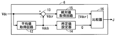
- Stability determination circuit 6 receives DC voltage Vdc and outputs stability determination signal J. The stability determination circuit 6 determines whether or not the DC voltage Vdc is not in an oscillation state. If the DC voltage Vdc is not in an oscillation state, the operation of the power converter is determined to be stable, and if it is in the oscillation state, the operation is unstable. judge.
- the DC voltage Vdc is in an oscillating state when the amplitude
- the stability determination circuit 6 contributes to the above determination by adopting, for example, the configuration shown in FIG. That is, the stability determination circuit 6 includes an average value acquisition circuit 12, a subtracter 13, a predetermined value setter 14, an absolute value acquisition circuit 15, and a comparator 16.
- the average value acquisition circuit 12 has a function of inputting the DC voltage Vdc, obtaining and outputting the average value Vdcb, and a low-pass filter, for example, is employed.
- the transfer function of the low-pass filter is represented by, for example, 1 / [1 + s ⁇ (1/30 / (2 ⁇ )] (“s” is a differential operator), where the cutoff frequency is set to 30 Hz. This is because the main frequency component of the pulsation component Vdcr is 300 Hz, which is six times the three-phase power supply frequency 50 Hz, so that the gain at 300 Hz is significantly attenuated.
- the subtractor 13 receives the DC voltage Vdc and the average value Vdcb, subtracts the average value Vdcb from the DC voltage Vdc, obtains a DC voltage pulsation component Vdcr, and outputs this.
- the absolute value acquisition circuit 15 receives the pulsation component Vdcr and takes the absolute value to obtain and output the amplitude
- the predetermined value setter 14 stores or generates a predetermined value Q and outputs it to the comparator 16.
- the comparator 16 is.
- of the pulsation component Vdcr are input, and the comparison result between them is output as the stability determination signal J.
- FIG. 3 shows the waveforms of the DC voltage Vdc, the pulsation Vdcr, its amplitude
- Vdcr the DC voltage
- the stability determination circuit 6 determines that the operation is stable, and sets the stability determination signal J to “L”.
- is equal to or greater than the predetermined value Q (or “larger than the predetermined value Q”), the DC power tsu Vdc is oscillating (the operation of the power converter 5 is unstable) and the stability determination is made.
- the circuit 6 makes the determination and sets the stability determination signal J to “H”.
- the inverter 1 inputs the stability determination signal J, and if it is “H”, the operation of the inverter 1 and then the operation of the power converter 5 is stopped.
- an unstable (oscillation) state may be indicated by outputting an error signal to the outside.
- the stability determination signal J does not faithfully represent the fluctuation of the magnitude relationship between the amplitude
- the predetermined value Q described above may be a fixed value, but is preferably set to a value that does not increase with respect to an increase in the average value Vdcb. This is because even when the operation of the power converter 5 is stable, the amplitude
- the power Pin input to the converter 8 is expressed by Expression (1) considering that it is a three-phase power source.
- E RMS value of input voltage
- I RMS value of input current
- ⁇ phase difference between input voltage and input current
- ⁇ angular frequency of input power source
- Equation (1) is a constant term
- the first term is a pulsation term. That is, when the pulsation component of the electric power Pin is Pinr, this is expressed by Expression (2).
- Equation (4) the differential equation represented by Equation (4) is established with respect to the DC voltage Vdc.
- Equation (5) a solution represented by Equation (5) is obtained.
- the second term of the lower equation of equation (5) represents the pulsation component Vdcr.
- the product E ⁇ I does not depend on the DC voltage Vdc, and the capacitance C of the capacitor 72 does not fluctuate. Therefore, although the pulsation component Vdcr fluctuates at a frequency six times the power supply frequency, its amplitude
- the predetermined value Q becomes smaller as the average value Vdcb increases in order to avoid erroneous detection. Is set.
- FIG. 4 illustrates a case where the predetermined value Q decreases linearly with respect to the increase of the average value Vdcb.
- the predetermined value Q may be inversely proportional to the average value Vdcb.
- an upper limit value Q1 and a lower limit value Q2 may be set for the predetermined value Q.
- the predetermined value Q is set smaller as the average value Vdcb increases between the upper limit value Q1 and the lower limit value Q2.
- the predetermined value Q takes the upper limit value Q1
- the predetermined value Q takes the lower limit value Q2.
- the predetermined value setter 14 may have, for example, a table that associates the average value Vdcb with the predetermined value Q, and has an arithmetic function that calculates using a mathematical formula for obtaining the predetermined value Q as a function of the average value Vdcb. It may be.
- the operation of the power conversion device is stable, it is erroneously determined as unstable or the operation of the power conversion device is unstable. Nevertheless, the possibility of misjudging it as stable is reduced.
- FIG. 6 illustrates the configuration of the power conversion apparatus according to the third embodiment.
- the power converter is modified with respect to the power converter 5 shown in the first embodiment in that an inductor 3 and a variable resistor 4 are provided in the DC link unit 7.
- the third embodiment is different from the first embodiment in that the stability determination signal J is not supplied to the inverter 1 but is used for controlling the variable resistor 4.
- a parallel connection is interposed between converter 8 and inverter 1.
- the parallel connection body is a parallel connection of an inductor 3 and a variable resistor 4.
- the inductor 3 forms a low-pass filter together with the capacitor 72.
- the resistance value of the variable resistor 4 is reduced when it is determined that the operation of the power converter is unstable.
- is compared with a predetermined value Q, and the stability determination signal J is “ Take the value of L "/" H ".
- the variable resistor 4 receives the value of the stability determination signal J when the amplitude of the pulsation amplitude
- variable resistor 4 By lowering the resistance value of the variable resistor 4, the current flowing through the inductor 3 is reduced, and the oscillation of the DC voltage Vdc is suppressed. That is, when it is determined that the operation of the power converter is unstable, the variable resistor 4 can be controlled to stabilize the power converter.
- the state of the stability determination signal J may be output to the outside to indicate an unstable (oscillation) state.
- FIG. 7 illustrates the configuration of the power conversion device 5 according to the fourth embodiment.
- the power converter differs from the power converter 5 shown in the first embodiment in that the stability determination signal J is not supplied to the inverter 1 but is input to the command value correction circuit 2. .
- the command value correction circuit 2 is illustrated as the frequency command correction circuit 2 in FIG.
- the frequency command correction circuit 2 corrects the frequency command f * based on the stability determination signal J, and gives the corrected frequency command (hereinafter referred to as “revised frequency command”) f ** to the inverter 1.
- the torque command correction circuit can be adopted as the frequency command correction circuit 2.
- the torque command correction circuit corrects the torque command T * based on the stability determination signal J, and gives the corrected torque command (hereinafter, “revised torque command”) T ** to the inverter 1.
- the inverter 1 normally inputs a frequency command f * or a torque command T * and operates based on these command values.
- the electric power output from the inverter 1 depends on these command values.
- the electric power W becomes It is expressed by 2 ⁇ ⁇ f ⁇ T / Pm ( ⁇ : pi). That is, as these command values are larger, the power output from the inverter 1, that is, the power supplied to the AC rotating machine 11 as a load is larger. As described in (e) above, the larger the output of the AC rotating machine 11, the more likely the operation of the power converter 5 becomes unstable.
- an inverter is used by using a command value, here, a revised frequency command f ** or a revised torque command T ** obtained by correcting the frequency command f * or the torque command T * to be small. Give to 1.
- the power output from the inverter 1 is, of course, proportional to the current and voltage output from the inverter 1.
- the inverter 1 operates based on the command value of the current or the command value of the voltage. Therefore, the electric power depends on the command value I * of the current output from the inverter 1. Alternatively, the electric power depends on the command value V * of the voltage output from the inverter 1.
- a current command correction circuit can be adopted as the frequency command correction circuit 2.
- the current command correction circuit corrects the current command I * based on the stability determination signal J, and gives the corrected current command (hereinafter referred to as “reformed current command”) I ** to the inverter 1.
- a voltage command correction circuit can be adopted as the frequency command correction circuit 2.
- the voltage command correction circuit corrects the voltage command V * based on the stability determination signal J, and gives the corrected voltage command (hereinafter referred to as “revision voltage command”) V ** to the inverter 1.
- the command value correction circuit 2 is the frequency command correction circuit 2
- a torque command correction circuit, a current command correction circuit, and a voltage command correction circuit may be employed as the command value correction circuit 2 from the above-described viewpoint regarding power.
- FIG. 8 is a circuit diagram illustrating the configuration of the frequency command correction circuit 2 according to the fourth embodiment.
- the frequency command correction circuit 2 includes a correction request circuit 21 and a command reduction circuit 22.
- the correction request circuit 21 receives the stability determination signal J and outputs a correction request signal K0.
- the command reduction circuit 22 inputs the frequency command f * and the correction request signal K0 and outputs the revised frequency command f **.
- the correction request circuit 21 includes an integrator 210 and a comparator 211.
- the integrator 210 integrates the stability determination signal J with a predetermined time constant and outputs an integration signal SJ.
- the stability determination signal J is “H” when it is determined that the operation of the power conversion device 5 is unstable. Therefore, the integration signal SJ is a period during which the stability determination signal J is “H”. Increases with length. For example, if it is grasped that the stability determination signal J is activated when the operation of the power converter 5 is unstable, the integration signal SJ corresponds to the length of the period during which the stability determination signal J is activated. It can be grasped that it increases.
- the comparator 211 activates the correction request signal K0 when the integration signal SJ exceeds the threshold value TH0.
- the command reduction circuit 22 includes a multiplier 220 and a changeover switch 221.
- the multiplier 220 multiplies the frequency command f * by a value larger than 0 and smaller than 1, for example, a value (1/2) and outputs the result.
- the changeover switch 221 has a contact A, a contact B, and a common contact C.
- the frequency command f * is given to the contact A, and the output of the multiplier 220 is given to the contact B. If the symbol f * is adopted as the value of the frequency command f *, the value given to the contact A is f * / 2.
- the common contact C is connected to the contact B / contact A in response to activation / deactivation of the correction request signal K0. Then, the revised frequency command f ** is taken out from the common contact C.
- FIG. 9 is a waveform diagram illustrating the operation of the frequency command correction circuit 2 according to the fourth embodiment.
- 4A shows the stability determination signal J
- FIG. 2B shows the integration signal SJ
- FIG. 2C shows the correction request signal K0
- FIG. 2D shows the counterpart connected to the common contact C.
- FIG. 5E shows the frequency change command f **.
- the activation / inactivation of the correction request signal K0 is indicated by an integer value 1/0.
- FIG. 6D the fact that the other party connected to the common contact C is the contact A is indicated by a smaller value than the case where the other party is the contact B.
- the stability determination signal J is “L” (inactive).
- the operation of the power converter 5 continues to be stable for a time sufficiently longer than the time constant for the integration of the integrator 210, and the integration signal SJ takes the value 0. . Therefore, the correction request signal K0 is inactive (value 0), the common contact C is connected to the contact A, and the revised frequency command f ** takes a value f * equal to the frequency command f *.
- the integration signal SJ increases. Even if the integration signal SJ reaches the threshold value TH0 at time t12, if the stability determination signal J remains “H”, the integration signal SJ exceeds the threshold value TH0, and the correction request signal K0 becomes active (value 1).
- the common contact C is connected to the contact B, and the revised frequency command f ** takes the value f ** / 2.
- the stability determination signal J becomes “L” (inactive), and the integration signal SJ decreases.
- the correction request signal K0 is deactivated, the common contact C is connected to the contact A, and the revised frequency command f ** takes the value f *.
- the operation of the power converter 5 operates again based on the original frequency command f *.
- the operation of the power converter 5 becomes unstable again by maintaining the command value once lowered due to the unstable operation of the power converter 5 even after the operation of the power converter 5 is stabilized. Can also be prevented. Such processing is easily realized by increasing the time constant of the integrator 210.
- FIG. 10 is a circuit diagram illustrating the configuration of the frequency command correction circuit 2 according to the fifth embodiment.
- the frequency command correction circuit 2 includes a correction request circuit 26 and a command reduction circuit 25.
- the correction request circuit 26 inputs the stability determination signal J and outputs correction request signals K1, K2, K3, K4.
- the command reduction circuit 25 inputs the frequency command f * and the correction request signals K1, K2, K3, and K4 and outputs the revised frequency command f **.
- the correction request circuit 26 includes an integrator 260 and comparators 261, 262, 263, and 264.
- the integrator 260 integrates the stability determination signal J with a predetermined time constant in the same manner as the integrator 210 (see the fourth embodiment), and outputs an integrated signal SJ.
- the comparator 261 activates the correction request signal K1 when the integration signal SJ exceeds the threshold value TH1.
- the comparator 262 activates the correction request signal K2 when the integration signal SJ exceeds the threshold value TH2.
- the comparator 263 activates the correction request signal K3 when the integration signal SJ exceeds the threshold value TH3.
- the comparator 264 activates the correction request signal K4 when the integration signal SJ exceeds the threshold value TH4.
- the threshold value TH2 is larger than the threshold value TH1
- the threshold value TH3 is larger than the threshold value TH2
- the threshold value TH4 is larger than the threshold value TH3. Therefore, the correction request signals K1, K2, K3 are always activated when the correction request signal K4 is activated, and the correction request signals K1, K2 are always activated when the correction request signal K3 is activated. When K2 is activated, the correction request signal K1 is always activated.
- the command reduction circuit 25 includes multipliers 255, 256, 257 and changeover switches 251, 252, 253, 254. Multipliers 255, 256, and 257 multiply the respective inputs by a value larger than 0 and smaller than 1, for example, all multiplied by a value (1/2) and output.
- the multiplier 255 is given a frequency command f * taking the value f * and outputs the value f * / 2.
- Multiplier 256 is supplied with the output of multiplier 255 and outputs the value f * / 4.
- Multiplier 257 is given the output of multiplier 256 and outputs the value f * / 8.
- the changeover switches 251, 252, 253, and 254 all have a contact A, a contact B, and a common contact C.
- the frequency command f * is given to the contact A, and the output from the common contact C of the changeover switch 252 is given to the contact B, respectively.
- the output from the multiplier 255 is given to the contact A, and the output from the common contact C of the changeover switch 253 is given to the contact B, respectively.
- the output of the multiplier 256 is given to the contact A, and the output from the common contact C of the changeover switch 254 is given to the contact B, respectively.
- the output of the multiplier 257 is given to the contact A.
- the contact B is given a value smaller than the output of the multiplier 257, here a value 0 smaller than the value f * / 8.
- the common contact C is connected to the contact B / contact A in response to the activation / deactivation of the correction request signal K1.
- the common contact C is connected to the contact B / contact A in response to the activation / deactivation of the correction request signal K2.
- the common contact C is connected to the contact B / contact A in response to the activation / inactivation of the correction request signal K3.
- the common contact C is connected to the contact B / contact A in response to activation / deactivation of the correction request signal K4.
- the revised frequency command f ** takes values classified as follows: correction request signals K1, K2, and so on. Value f * when all of K3 and K4 are inactive; value f * / 2 when only correction request signal K1 is active; value f * / 4 when only correction request signals K1 and K2 are active; correction request signal K1 , K2, K3 only when the value is f * / 8; when the correction request signals K1, K2, K3, K4 are all active, the value is 0.
- 11 and 12 are waveform diagrams illustrating the operation of the frequency command correction circuit 2 according to the fifth embodiment.
- the instability of the operation of the power conversion device 5 is more remarkable than in the case illustrated in FIG. 12.
- the stability determination signal J is “L”.
- the operation of the power converter 5 continues to be stable for a time sufficiently longer than the time constant for the integration of the integrator 260, and the integration signal SJ takes the value 0. . Therefore, the correction request signals K1, K2, K3, and K4 are inactive, and the revised frequency command f ** takes a value f * that is equal to the frequency command f *.
- the integration signal SJ increases.
- the correction request signal K1 is activated, and the revised frequency command f ** takes the value f * / 2.
- the stability determination signal J remains “H” and the integration signal SJ continues to rise.
- the integration signal SJ reaches the threshold value TH2, the correction request signal K2 is also activated, and the frequency change command f ** takes the value f * / 4.
- the stability determination signal J remains “H” and the integration signal SJ continues to rise.
- the integration signal SJ reaches the threshold value TH3
- the correction request signal K3 is also activated, and the frequency change command f ** takes the value f * / 8.
- the stability determination signal J remains “H” and the integration signal SJ continues to rise.
- the integration signal SJ reaches the threshold value TH4, the correction request signal K4 is also activated, and the frequency change command f ** takes the value 0.
- the integration signal SJ increases.
- the correction request signal K1 is activated, and the revised frequency command f ** takes the value f * / 2.
- the stability determination signal J remains “H” and the integration signal SJ continues to rise.
- the integration signal SJ reaches the threshold value TH2, the correction request signal K2 is also activated, and the frequency change command f ** takes the value f * / 4.
- the stability determination signal J maintains “H” and the integration signal SJ continues to rise, but does not reach the threshold value TH3.
- the stability determination signal J takes “L” and integration. The signal SJ decreases.
- the integration signal SJ falls below the threshold value TH2
- the correction request signal K2 is deactivated, and the frequency change command f ** takes the value f * / 2.
- the stability determination signal J remains “L” and the integrated signal SJ continues to decrease.
- the integrated signal SJ falls below the threshold value TH1
- the correction request signal K1 becomes inactive
- the frequency change command f ** takes the value f *.
- the revised frequency command f ** may alternately take values f * / 2 and f * / 4.
- FIG. 13 is a circuit diagram illustrating the configuration of the frequency command correction circuit 2 according to the sixth embodiment.
- the frequency command correction circuit 2 includes an integrator 23 and a subtracter 24.
- the integrator 23 inputs the stability determination signal J and outputs an integration signal SJ.
- the subtracter 23 inputs the frequency command f * and the integration signal SJ and outputs the revised frequency command f **. That is, in the sixth embodiment, the integral signal SJ that increases according to the length of the period in which the operation of the power conversion device 5 is determined to be unstable (that is, the stability determination signal J is activated) It will be subtracted from the command value on which the power depends.
- Such subtraction is different from the stepwise switching of the revised frequency command f ** as shown in the fourth embodiment or the fifth embodiment. That is, since the revised frequency command f ** can be obtained with a reduction amount necessary for the operation of the power converter 5 to be stable, the revised frequency command f ** is not excessively lowered.
- FIG. 14 and 15 are waveform diagrams illustrating the operation of the frequency command correction circuit 2 according to the sixth embodiment.
- the instability of the operation of the power conversion device 5 is more remarkable than in the case illustrated in FIG. 14.
- the stability determination signal J is “L”.
- the operation of the power converter 5 continues to be stable for a time sufficiently longer than the time constant for the integration of the integrator 23, and the integration signal SJ takes the value 0. . Therefore, the revised frequency command f ** takes a value f * equal to the frequency command f *.
- the revised frequency command f ** decreases, the operation of the power converter 5 is led to stability, and it is determined that the operation of the power converter 5 is stable at time t42. As a result, the stability determination signal J becomes “L” and the integral signal SJ decreases. Along with this, the revised frequency command f ** increases. Thereafter, when it is determined that the operation of the power conversion device 5 is unstable again, the revised frequency command f ** decreases.
- the revised frequency command f ** is set so large that the operation of the power converter 5 can be stabilized.
- the stability determination signal J is “L”.
- the operation of the power converter 5 continues to be stable for a time sufficiently longer than the time constant for the integration of the integrator 23, and the integration signal SJ takes the value 0. . Therefore, the revised frequency command f ** takes a value f * equal to the frequency command f *.
- the stability determination signal J is maintained at “H”, and the integration signal SJ continues to rise.
- the revised frequency command f ** takes the value 0.
- the decrease in the revised frequency command f ** is halved, but it may be decreased at a reduction rate other than this. That is, the multipliers 250, 255, 256, and 257 can employ values other than the value (1/2) and larger than 0 and smaller than 1. Further, the thresholds TH1 to TH4 can be set appropriately as long as the magnitude relationship between them is not impaired.
- the amount of decrease in the revised frequency command f ** is proportional to the integrated signal SJ.
- the subtractor 24 may add a positive weight to the integration signal SJ and subtract it from the frequency command f *.
- the revised torque command T **, the revised current command I **, and the revised voltage command V ** can be used instead of the revised frequency command f **. .
- the operation of the stability determination circuit 6 can be grasped as a stability determination method.
- the power converter 5 described above is clearly different from the conventional technique in that such a stability determination method is adopted.
- the converter 8, the inverter 1, the DC buses 70 and 71, the capacitor 72, and the stability determination circuit 6 can also be grasped as a power conversion device.
- the correction circuit 2 can also be grasped as a power conversion device for such a configuration.
Landscapes
- Engineering & Computer Science (AREA)
- Power Engineering (AREA)
- Inverter Devices (AREA)
Abstract
電力変換装置においてコンデンサの静電容量が小さくて種々の条件によって直流電圧が振動して不安定になったとき、これを検知する。安定性判定回路6は平均値取得回路12、減算器13、所定値設定器14、絶対値取得回路15、比較器16を有する。平均値取得回路12は直流電圧Vdcの平均値Vdcbを得る。減算器13は直流電圧Vdcから平均値Vdcbを差し引いて直流電圧の脈動分Vdcrを得る。絶対値取得回路15は脈動分Vdcrの絶対値|Vdcr|を得る。所定値設定器14は所定値Qを出力する。比較器16は所定値Qと、脈動分Vdcrの振幅|Vdcr|との比較結果を安定判定信号Jとして出力する。所定値Qは固定値、あるいは平均値Vdcbの増加に対して非増加となる値を採る。
Description
本発明は交流を一旦直流に変換し、更に当該直流を交流へ変換する電力変換装置、及びその安定性を判定する技術に関する。
従来、交流電力を整流して直流電力を得て、当該直流に対してスイッチングを施して可変電圧、可変周波数の交流電力に変換する電力変換装置が広く利用されている。当該電力変換装置は、例えば変換後の交流電力で三相交流回転機を可変速制御することに資する。
このような電力変換装置の一種として、一対の直流母線で相互に接続されたコンバータ及びインバータを備え、かつ当該一対の直流母線の間にコンデンサが接続される構成が知られている。
コンバータは交流電圧、例えば商用電源から供給される三相交流電圧を全波整流して直流電圧に変換する。当該コンバータとしては例えばダイオードブリッジが採用される。
インバータは、コンバータで得られた直流電圧をスイッチングして三相交流電圧に変換する。当該三相交流電圧は、負荷である三相の交流回転機に供給される。
インバータはスイッチング素子を有しており、スイッチング素子の動作が制御されることにより、その出力端子から所望の周波数の三相交流電圧を負荷へ出力する。
上記コンデンサは、これが平滑回路あるいはその一部として採用される場合には、交流回転機の駆動性能の向上を図るために、静電容量が大きいことが要求される。かかる静電容量の大きなコンデンサを得るには電解コンデンサが適しているが、そのリップル電流の耐量による制限からも大きな静電容量が望まれる。
しかしながら、このような大容量のコンデンサの採用は、電力変換装置が大きくなることや製作コストを増大させる課題がある。
他方、当該コンデンサとして平滑機能を優先せず、数十μF程度の小容量のコンデンサを使用する技術があり、下掲の特許文献1,2や非特許文献1において開示されている。
特許文献1,2では、コンデンサの静電容量を小さくすることで、電源トランス等を含む交流電源のインピーダンス(以下、電源インピーダンスという)や配線のインピーダンス(以下、配線インピーダンスという)により系が不安定になることが示されている。特許文献1,2では系が不安定となる条件が主に以下であることも示されている。
(a)コンデンサの容量が小さいほど不安定になりやすい。
(b)電源および配線等の抵抗分が小さいほど不安定になりやすい。
(c)電源および配線のインダクタンス分が大きいほど不安定になりやすい。
(d)直流電圧が低いほど不安定になりやすい。
(e)電動機出力が大きいほど不安定になりやすい。
(a)コンデンサの容量が小さいほど不安定になりやすい。
(b)電源および配線等の抵抗分が小さいほど不安定になりやすい。
(c)電源および配線のインダクタンス分が大きいほど不安定になりやすい。
(d)直流電圧が低いほど不安定になりやすい。
(e)電動機出力が大きいほど不安定になりやすい。
特許文献1には、電源側のインピーダンス条件によっては直流母線間の電圧が振動し易くなり、制御系が不安定になることに鑑みて、制御系を安定に保つべく出力電圧指令補正を制御する技術について記載されている。
高橋 勲・伊東洋一「コンデンサレスインバータの制御法」昭和63年電気学会全国大会、Vol.5,No.527、p624
特許文献1に記載している方法では、電源インピーダンスと配線インピーダンスの状態に加えて、交流電源の電圧が低い場合に、直流電圧が振動して系が不安定になる可能性がある。
そして特許文献1の方式ではこの不安定を検知していないので、系が不安定になった場合に、直流電圧が大きく振動することによりインバータを構成する部品やコンデンサの寿命を短くし、引いてはそれらの故障を招来する。
本発明は、上記の問題点を解決するためになされたものであり、電力変換装置においてコンデンサの静電容量が小さくて種々の条件によって直流電圧が振動して電力変換装置の動作が不安定になったとき、これを検知する技術を提供することを目的としている。
この発明にかかる安定性判定方法は、コンバータ(8)と、インバータ(1)と、前記コンバータと前記インバータとを接続する一対の直流母線(70,71)と、前記一対の直流母線の間に接続されるコンデンサ(72)とを備える電力変換装置(5)における動作の安定性を判定する方法である。
この発明にかかる安定性判定方法の第1の態様では、前記一対の直流母線の間の直流電圧(Vdc)の脈動分(Vdcr)の振幅(|Vdcr|)が、所定値(Q)を超えることを以て、前記電力変換装置の動作が不安定であると判定される。
この発明にかかる安定性判定方法のその第2の態様は、安定性判定方法の第1の態様であって、前記所定値(Q)を前記平均値(Vdcb)の増加に対して非増加となる値に設定する。
この発明にかかる安定性判定方法の第3の態様は安定性判定方法の第1の態様または第2の態様である。当該第3の態様において、電力変換装置には前記一対の直流母線の一方(71)において、前記コンバータ(8)と前記インバータ(1)との間に、並列接続体が介在する。前記並列接続体は、前記コンデンサ(72)と共にローパスフィルタを形成するインダクタ(3)と、前記インダクタと並列に接続された可変抵抗(4)とを有する。そして前記電力変換装置の動作が不安定であると判定された場合、前記可変抵抗の抵抗値が低減される。
この発明にかかる安定性判定方法の第4の態様は安定性判定方法の第1の態様または第2の態様である。当該第4の態様において、前記電力変換装置の動作が不安定であると判定された場合、前記インバータから出力される電力を低減する。
当該第4の態様として望ましくは、前記電力変換装置の動作が不安定であると判定された期間の長さに対応して増大する信号(SJ)が所定の閾値(TH0,TH1,TH2,TH3,TH4)を超えることに対応して、前記電力を低減する。
この発明にかかる安定性判定方法の第5の態様はその第4の態様であって、前記電力変換装置の動作が不安定であると判定された期間の長さに対応して増大する信号(SJ)を、前記電力が依存する指令値(f*,T*,I*,V*)から減じる。
この発明にかかる安定性判定回路(6)は、コンバータ(8)と、インバータ(1)と、前記コンバータと前記インバータとを接続する一対の直流母線と、前記一対の直流母線の間に接続されるコンデンサ(72)とを備える電力変換装置における動作の安定性を判定する回路である。
この発明にかかる安定性判定回路の第1の態様は、前記一対の直流母線の間の直流電圧の平均値(Vdcb)を得る平均値取得回路(12)と、前記直流電圧から前記平均値を差し引いて前記直流電圧の脈動分(Vdcr)を得る減算器(13)と、前記脈動分の振幅(|Vdcr|)を求める絶対値取得回路(15)と、所定値(Q)を設定する所定値設定器(14)と、前記所定値と前記振幅とを比較する比較器(16)とを備える。
この発明にかかる安定性判定回路の第2の態様は、安定性判定回路の第1の態様であって、前記所定値(Q)は、前記平均値(Vdcb)の増加に対して非増加となる値に設定される。
この発明にかかる電力変換装置(5)の第1の態様は、コンバータ(8)と、インバータ(1)と、前記コンバータと前記インバータとを接続する一対の直流母線(70,71)と、前記一対の直流母線の間に接続されるコンデンサ(72)とを備え、前記一対の直流母線の一方において、前記コンバータ(8)と前記インバータ(1)との間に介在する並列接続体を更に備える。前記並列接続体は、前記コンデンサ(72)と共にローパスフィルタを形成するインダクタ(3)と、前記インダクタと並列に接続された可変抵抗(4)とを有する。そしてこの発明にかかる安定性判定方法の第1の態様又は第2の態様によって、前記電力変換装置の動作が不安定であると判定された場合、前記可変抵抗の抵抗値が低減する。
この発明にかかる電力変換装置(5)の第2の態様は、コンバータ(8)と、インバータ(1)と、前記コンバータと前記インバータとを接続する一対の直流母線(70,71)と、前記一対の直流母線の間に接続されるコンデンサ(72)とを備え、安定性判定回路(6)と、修正回路(2)とを更に備える。前記安定性判定回路は、前記一対の直流母線の間の直流電圧の平均値(Vdcb)を得る平均値取得回路(12)と、前記直流電圧から前記平均値を差し引いて前記直流電圧の脈動分(Vdcr)を得る減算器(13)と、前記脈動分の振幅(|Vdcr|)を求める絶対値取得回路(15)と、所定値(Q)を設定する所定値設定器(14)とを有する。そして前記修正回路(2)は、前記振幅が前記所定値よりも大きい場合、前記インバータの出力する電力が依存する指令値(f*,T*,I*,V*)を小さく修正して前記インバータに出力する。
望ましくは、前記所定値(Q)は、前記平均値(Vdcb)の増加に対して非増加となる値に設定される。
あるいは望ましくは、前記振幅が前記所定値よりも大きい期間の長さに対応して増大する信号(SJ)が所定の閾値(TH0,TH1,TH2,TH3,TH4)を超えることに対応して、前記指令値(f*,T*,I*,V*)が小さく修正される。
あるいは望ましくは、前記振幅が前記所定値よりも大きい期間の長さに対応して増大する信号(SJ)を、前記指令値(f*,T*,I*,V*)から減じる。
電力変換装置の動作が不安定となるときには、電力変換装置の動作が安定となるときと比較して、直流電圧の脈動分が増大する。よってこの発明にかかる安定判定方法の第1の態様によれば、脈動分が所定値を越えることによって電力変換装置の動作が不安定であると判定することができる。
直流電圧の脈動分の振幅は、電力変換装置の動作が安定であるときでも、直流電圧の平均値の増大に伴って減少する。よってこの発明にかかる安定判定方法の第2の態様によれば、直流電圧の平均値が小さいときに、実際には電力変換装置の動作が安定であるにも拘わらずこれを不安定であると誤判定したり、実際には電力変換装置の動作が不安定であるにも拘わらずこれを安定であると誤判定したりする可能性を低減する。
この発明にかかる安定性判定回路の第1の態様及び第2の態様は、それぞれこの発明にかかる安定判定方法の第1の態様及び第2の態様の実行に資する。
インダクタが設けられてローパスフィルタが構成される電力変換装置において、インダクタに流れる電流を低減することにより、直流電圧の変動は小さくなる。よってこの発明にかかる安定判定方法の第3の態様及びこの発明にかかる電力変換装置の第1の態様によれば、電力変換装置の動作が不安定なときに可変抵抗の抵抗を小さくし、以てインダクタに流れる電流を小さくすることにより、電力変換装置の動作を安定にすることができる。
インバータから出力される電力が小さいほど、電力変換器の動作は安定性へと導かれる。よってこの発明にかかる安定判定方法の第4の態様によれば、電力変換装置の動作を安定にすることができる。
インバータから出力される電力は、当該電力が依存する指令値が小さいほど低減される。よってこの発明にかかる安定判定方法の第5の態様及びこの発明にかかる電力変換装置の第2の態様によれば、電力変換装置の動作を安定にすることができる。
この発明の目的、特徴、局面、および利点は、以下の詳細な説明と添付図面とによって、より明白となる。
第1の実施の形態.
図1は第1の実施の形態にかかる電力変換装置5の構成を例示する。電力変換装置5は、コンバータ8と、インバータ1と、コンバータ8とインバータ1とを接続する直流リンク部7とを備えている。
図1は第1の実施の形態にかかる電力変換装置5の構成を例示する。電力変換装置5は、コンバータ8と、インバータ1と、コンバータ8とインバータ1とを接続する直流リンク部7とを備えている。
コンバータ8は交流電源10(ここでは三相交流電源)から得られる交流電圧を整流して直流電圧に変換する。ここではコンバータ8として三相の全波整流ダイオードブリッジが採用されているが、他の整流回路を採用することもできる。
ここではコンバータ8は交流電源10からリアクトル群9を介して各相電圧を入力している場合が例示されている。リアクトル群9を電力変換装置5に含めて把握してもよい。
直流リンク部7は一対の直流母線70,71を有しており、直流母線71は直流母線70よりも高電位が印加される。直流母線70,71はコンバータ8とインバータ1とを接続する。直流母線70,71の間にはコンデンサ72が接続されている。直流母線70,71の間には、従ってコンデンサ72の両端には、直流電圧Vdcが印加される。なお図1では、直流リンク部7における寄生インダクタ73及び寄生抵抗74も示されている。
コンデンサ72としては、上記特許文献1,2や非特許文献1で示されるような、平滑回路として要求される静電容量よりも小さな、例えば数十μF程度の静電容量のコンデンサが採用される。
インバータ1は直流電圧Vdcをスイッチングすることにより、所望の周波数の交流電圧、ここでは三相交流電圧を出力する。そして当該交流電圧は負荷11(ここでは交流回転機)に印加される。
なお、交流回転機とは、同期機か誘導機かあるいは他の種類のモータをも含む。
なお、説明の簡単のため、インバータ1としては上記スイッチングを行うスイッチング素子の他、当該スイッチングを制御する制御信号を生成する回路も含めて把握している。
安定性判定回路6は直流電圧Vdcを入力し、安定判定信号Jを出力する。安定性判定回路6は、直流電圧Vdcが発振状態にないかどうかを判定し、発振状態になければ電力変換装置の動作が安定と判定し、発振状態にあれば当該動作が不安定であると判定する。
具体的には、直流電圧Vdcの脈動分Vdcrの振幅|Vdcr|が、所定値Qを超えることを以て、直流電圧Vdcが発振状態にあると判定する。
安定性判定回路6は、例えば図2に示される構成を採ることにより、上記判定に資する。即ち、安定性判定回路6は平均値取得回路12、減算器13、所定値設定器14、絶対値取得回路15、比較器16を有する。
平均値取得回路12は、直流電圧Vdcを入力し、その平均値Vdcbを得て出力する機能を担い、例えばローパスフィルタが採用される。当該ローパスフィルタの伝達関数は、例えば、1/[1+s・(1/30/(2π)]で示される(「s」は微分演算子)。ここでカットオフ周波数は30Hzに設定している。これは、脈動成分Vdcrの主な周波数成分は三相電源周波数50Hzの6倍である300Hzであることに鑑み、300Hzにおけるゲインを顕著に減衰させるためである。
なお、直流電圧Vdcを測定する技術については公知であるので、ここではその詳細を割愛する。
減算器13は直流電圧Vdcと平均値Vdcbとを入力し、直流電圧Vdcから平均値Vdcbを差し引いて直流電圧の脈動分Vdcrを得て、これを出力する。
絶対値取得回路15は脈動分Vdcrを入力してその絶対値を採ることにより、その振幅|Vdcr|を得て出力する。
所定値設定器14は所定値Qを記憶、若しくは生成し、これを比較器16へと出力する。
比較器16は。所定値設定器14が出力した所定値Qと、脈動分Vdcrの振幅|Vdcr|とを入力し両者の比較結果を安定判定信号Jとして出力する。
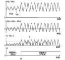
図3に、直流電圧Vdc、脈動分Vdcr及びその振幅|Vdcr|及び安定判定信号Jの波形を示す。ここでは時刻t1において直流電圧Vdcが発振した場合を例示している。
直流電圧Vdcが発振すると、その振動幅が急激に増大する。但し、平均値Vdcbは殆ど変動せず、脈動分Vdcrの振幅|Vdcr|が急激に増大する。換言すれば、電力変換装置5の動作が不安定となるときには、電力変換装置5の動作が安定となるときと比較して、直流電圧Vdcの脈動分Vdcrが増大する。よって絶対値取得回路15から得られた振幅|Vdcr|が所定値Qよりも低い(あるいは「所定値Q以下である」)場合には、直流電津Vdcは発振していない(電力変換装置5の動作が安定している)と安定性判定回路6が判定し、安定判定信号Jを“L”とする。振幅|Vdcr|が所定値Q以上である(あるいは「所定値Qより大きい」)場合には、直流電津Vdcは発振している(電力変換装置5の動作が不安定である)と安定性判定回路6が判定し、安定判定信号Jを“H”とする。
インバータ1は安定判定信号Jを入力し、それが“H”であればインバータ1の、引いては電力変換装置5の動作を停止する。もしくは、外部にエラー信号を出力するようにして、不安定(発振)状態を示すようにしてもよい。
以上のようにして、直流電圧Vdcが振動して電力変換装置5の動作が不安定になったとき、これを検知し、あるいはその動作を停止することができる。これは電力変換装置5の故障や、その部品の短命化を回避する観点で望ましい。
ここでは安定判定信号Jは振幅|Vdcr|と所定値Qとの大小関係の変動を忠実に表さず、安定判定信号Jが一旦“H”となれば、これを持続する態様が例示されている。例えば、安定判定信号Jが一旦“H”となった後は、電源周期の1/6よりも長い周期に亘って振幅|Vdcr|が所定値Qよりも小さくなって初めて安定判定信号Jが“L”とする。これにより、振幅|Vdcr|の波形を考慮した、直流電圧Vdcの発振を検知することができる。
安定判定信号Jの“L”/“H”と直流電圧Vdcの安定/不安定の対応は上述の対応とは逆であってもよい。
第2の実施の形態.
上述の所定値Qは固定値であってもよいが、平均値Vdcbの増加に対して非増加となる値に設定されることが望ましい。電力変換装置5の動作が安定であるときでも、直流電圧Vdcの平均値Vdcrが大きくなるほど脈動分Vdcrの振幅|Vdcr|は小さくなる傾向があるからである。かかる傾向があるため、所定値Qが固定値であれば、平均値Vdcbが小さい場合において安定に動作している電力変換装置5を不安定であると誤検知したり、平均値Vdcbが大きい場合において動作が不安定な電力変換装置5を安定に動作していると誤検知したりする可能性がある。
上述の所定値Qは固定値であってもよいが、平均値Vdcbの増加に対して非増加となる値に設定されることが望ましい。電力変換装置5の動作が安定であるときでも、直流電圧Vdcの平均値Vdcrが大きくなるほど脈動分Vdcrの振幅|Vdcr|は小さくなる傾向があるからである。かかる傾向があるため、所定値Qが固定値であれば、平均値Vdcbが小さい場合において安定に動作している電力変換装置5を不安定であると誤検知したり、平均値Vdcbが大きい場合において動作が不安定な電力変換装置5を安定に動作していると誤検知したりする可能性がある。
以下、上記傾向が発生する理由について説明する。今、コンバータ8に入力する電力Pinは、三相電源であることを考慮すると、式(1)で表される。

なお、E:入力電圧の実効値、I:入力電流の実効値、φ:入力電圧と入力電流の位相差、ω:入力電源の角周波数とした。
コンバータ8でのインダクタンスが小さく、力率がほぼ1であることを考慮すると、cosφ=1と近似できる。よって式(1)の第2項が定数項となり、第1項が脈動項となる。つまり、電力Pinの脈動成分をPinrとすると、これは式(2)で表される。

一方、直流電圧Vdcの脈動は負荷11へ影響を与えないと考えられ、コンデンサ72の容量をCとして式(3)が成立する。

式(2)を式(3)に代入して、直流電圧Vdcに対して式(4)で表される微分方程式が成立する。

直流電圧Vdcの平均値Vdcbを初期値として式(4)の微分方程式を解くと、式(5)で表される解が得られる。但し、上側の式の平方根の中の第2項は第1項に対して小さいので、近似して下側の式を得ている(εが1より十分に小さいときの√(1+ε)=1+ε/2とする近似と同様)。

式(5)の下側の式の第2項は、脈動成分Vdcrを表していることになる。積E・Iは直流電圧Vdcに依存せず、コンデンサ72の容量Cも変動しないので、脈動成分Vdcrは電源周波数の6倍の周波数で変動するものの、その振幅|Vdcr|は平均値Vdcbに反比例することが判る。以上のようにして、上述の傾向があることがわかる。
かかる傾向に鑑みて、直流電圧Vdcの発振の有無、引いては電力変換装置5の安定性を判断するに際しては、その誤検知を回避すべく、所定値Qは平均値Vdcbが増加するほど小さく設定される。図4は所定値Qが平均値Vdcbの増加に対して線形に減少する場合を例示している。もちろん、式(5)に鑑みて、所定値Qが平均値Vdcbに反比例してもよい。
あるいは図5に示されるように、所定値Qに対して上限値Q1及び下限値Q2を設定してもよい。平均値Vdcbが値B1~B2(>B1)の間を採るとき、所定値Qは上限値Q1及び下限値Q2の間で平均値Vdcbが増加するほど小さく設定される。平均値Vdcbが値B1以下の値を採るとき所定値Qは上限値Q1をとり、平均値Vdcbが値B2以上の値を採るとき所定値Qは下限値Q2を採る。
このように所定値Qを設定するために、図2において破線で示されるように、所定値設定器14には平均値Vdcbが入力されることが望ましい。所定値設定器14は例えば平均値Vdcbと所定値Qとを対応づけるテーブルを有していてもよいし、平均値Vdcbの関数として所定値Qを求める数式を用いて計算する演算機能を有していてもよい。
以上のようにして第2の実施の形態によれば、電力変換装置の動作が安定であるにも拘わらずこれを不安定であると誤判定したり、電力変換装置の動作が不安定であるにも拘わらずこれを安定であると誤判定したりする可能性を低減する。
第3の実施の形態.
図6は第3の実施の形態にかかる電力変換装置の構成を例示する。当該電力変換装置は、第1の実施の形態で示された電力変換装置5に対し、直流リンク部7にインダクタ3及び可変抵抗4が設けられている点で変形されている。また安定判定信号Jはインバータ1に供給されるのではなく、可変抵抗4の制御に採用されている点でも、第3の実施の形態は第1の実施の形態と相違する。
図6は第3の実施の形態にかかる電力変換装置の構成を例示する。当該電力変換装置は、第1の実施の形態で示された電力変換装置5に対し、直流リンク部7にインダクタ3及び可変抵抗4が設けられている点で変形されている。また安定判定信号Jはインバータ1に供給されるのではなく、可変抵抗4の制御に採用されている点でも、第3の実施の形態は第1の実施の形態と相違する。
より具体的には直流母線71において、コンバータ8とインバータ1との間に並列接続体が介在している。当該並列接続体はインダクタ3と可変抵抗4の並列接続である。
インダクタ3はコンデンサ72と共にローパスフィルタを形成する。可変抵抗4の抵抗値は、当該電力変換装置の動作が不安定であると判定された場合に低減される。
具体的には、第1の実施の形態及び第2の実施の形態で説明されたようにして、脈動分の振幅|Vdcr|の大きさが所定値Qと比較され、安定判定信号Jは“L”/“H”の値を採る。そして可変抵抗4は、脈動分の振幅|Vdcr|の大きさが所定値Qよりも大きい(あるいは「所定値Q以上」)ときの安定判定信号Jの値を受けて、その抵抗値が下げられる。
このようにして可変抵抗4の抵抗値を下げることにより、インダクタ3に流れる電流を低減し、直流電圧Vdcの発振を抑制する。つまり電力変換装置の動作が不安定であると判定された場合、可変抵抗4を制御して電力変換装置を安定にすることができる。
このとき、可変抵抗4に流れる電流は小さく、直流電流Vdcに与える影響は小さい。よって可変抵抗4の制御によって安定性判定に支障は生じない。
もちろん、安定判定信号Jの状況を外部に出力するようにして、不安定(発振)状態を示すようにしてもよい。
第4の実施の形態.
図7は第4の実施の形態にかかる電力変換装置5の構成を例示する。当該電力変換装置は、第1の実施の形態で示された電力変換装置5に対し、安定判定信号Jはインバータ1に供給されるのではなく、指令値修正回路2に入力する点で相違する。
図7は第4の実施の形態にかかる電力変換装置5の構成を例示する。当該電力変換装置は、第1の実施の形態で示された電力変換装置5に対し、安定判定信号Jはインバータ1に供給されるのではなく、指令値修正回路2に入力する点で相違する。
指令値修正回路2は図7では周波数指令修正回路2として例示される。周波数指令修正回路2は、周波数指令f*を安定判定信号Jに基づいて修正し、修正された周波数指令(以下「改周波数指令」)f**をインバータ1に与える。
周波数指令修正回路2にはトルク指令修正回路を採用することもできる。この場合、トルク指令修正回路は、トルク指令T*を安定判定信号Jに基づいて修正し、修正されたトルク指令(以下「改トルク指令」)T**をインバータ1に与える。
第1乃至第3の実施の形態では、説明を省略したが、インバータ1は通常、周波数指令f*若しくはトルク指令T*を入力し、これらの指令値に基づいて動作する。インバータ1が出力する電力はこれらの指令値に依存する。
例えば交流回転機11の回転周波数f(これの指令値が周波数指令f*)と、出力トルクT(これの指令値がトルク指令T*)と、極対数Pmとを導入すると、その電力Wは2π・f・T/Pmで表される(π:円周率)。つまりこれらの指令値が大きいほど、インバータ1が出力する電力、即ち負荷たる交流回転機11に与えられる電力が大きい。そして上記(e)で述べたように、交流回転機11の出力が大きいほど、電力変換装置5の動作が不安定になりやすい。
そこで、電力変換装置5の動作が不安定であると判定された場合、インバータ1から出力される電力を低減することにより、動作が安定へと導かれる。かかる電力低減のために、具体的には指令値、ここでは周波数指令f*若しくはトルク指令T*を小さく修正して得られる改周波数指令f**若しくは改トルク指令T**を用いて、インバータ1に与える。
インバータ1が出力する電力は、当然ながら、インバータ1が出力する電流及び電圧に比例する。インバータ1は当該電流の指令値、もしくは当該電圧の指令値に基づいて動作する。よって当該電力は、インバータ1が出力する電流の指令値I*に依存する。あるいは当該電力はインバータ1が出力する電圧の指令値V*に依存する。
従って、周波数指令修正回路2には電流指令修正回路を採用することもできる。この場合、電流指令修正回路は、電流指令I*を安定判定信号Jに基づいて修正し、修正された電流指令(以下「改電流指令」)I**をインバータ1に与える。
あるいは、周波数指令修正回路2には電圧指令修正回路を採用することもできる。この場合、電圧指令修正回路は、電圧指令V*を安定判定信号Jに基づいて修正し、修正された電圧指令(以下「改電圧指令」)V**をインバータ1に与える。
第4乃至第6実施の形態では指令値修正回路2が周波数指令修正回路2である場合について説明する。但し、電力についての上述の観点から、指令値修正回路2としてトルク指令修正回路、電流指令修正回路、電圧指令修正回路を採用してもよい。
図8は、第4の実施の形態にかかる周波数指令修正回路2の構成を例示する回路図である。周波数指令修正回路2は、修正要求回路21と指令低減回路22とを有する。
修正要求回路21は、安定判定信号Jを入力して修正要求信号K0を出力する。指令低減回路22は、周波数指令f*及び修正要求信号K0を入力して改周波数指令f**を出力する。
修正要求回路21は、積分器210と比較器211とを有する。積分器210は安定判定信号Jを所定の時定数で積分して積分信号SJを出力する。安定判定信号Jは、上述のように、電力変換装置5の動作が不安定であると判定するときに“H”となるので、積分信号SJは安定判定信号Jが“H”となる期間の長さに対応して増大する。例えば安定判定信号Jは、電力変換装置5の動作が不安定であることを示す場合に活性化する、と把握すれば、積分信号SJは安定判定信号Jが活性化する期間の長さに対応して増大すると把握することができる。
比較器211は積分信号SJが閾値TH0を越えることにより、修正要求信号K0を活性化させる。
指令低減回路22は、乗算器220と、切替スイッチ221とを有する。乗算器220は周波数指令f*に対して0より大きく1より小さい値、例えば、値(1/2)を乗じて出力する。
切替スイッチ221は、接点A、接点B、共通接点Cを有する。接点Aには周波数指令f*が、接点Bには乗算器220の出力が、それぞれ与えられる。周波数指令f*が有する値としても記号f*を採用すれば、接点Aに与えられる値はf*/2となる。
共通接点Cは、修正要求信号K0の活性/非活性に対応してそれぞれ接点B/接点Aと接続される。そして共通接点Cから改周波数指令f**が取り出される。
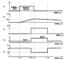
図9は、第4の実施の形態にかかる周波数指令修正回路2の動作を例示する波形図である。同図(a)は安定判定信号Jを、同図(b)は積分信号SJを、同図(c)は修正要求信号K0を、同図(d)は共通接点Cと接続される相手を、同図(e)は改周波数指令f**を、それぞれ示す。但し、同図(c)において、修正要求信号K0の活性/非活性はそれぞれ整数値1/0で示される。また同図(d)において、共通接点Cと接続される相手が接点Aであることを、当該相手が接点Bである場合よりも値が小さいことで示す。
図9の例示では、時刻t11以前には電力変換装置5の動作が安定であると判定され、安定判定信号Jが“L”(非活性)となっている。ここでは時刻t11において既に、積分器210の積分についての時定数よりも十分に長い間、電力変換装置5の動作が安定し続けている場合を想定しており、積分信号SJは値0を採る。よって修正要求信号K0は非活性(値0)であり、共通接点Cは接点Aと接続され、改周波数指令f**は周波数指令f*と等しい値f*を採る。
そして時刻t11において電力変換装置5の動作が不安定であると判定され、安定判定信号Jが“H”(活性)となると、積分信号SJは上昇する。時刻t12において積分信号SJが閾値TH0に到達しても安定判定信号Jが“H”を維持していれば、積分信号SJが閾値TH0を越え、修正要求信号K0が活性(値1)となり、共通接点Cは接点Bと接続され、改周波数指令f**は値f*/2を採る。
このように改周波数指令f**が低下すると、インバータ1が出力する電力が低下し、電力変換装置5の動作は安定化へと導かれる。このようにして指令値を下げることにより、電力を低減し、以て電力変換装置5の動作を安定にすることができる。
これにより、時刻t13において電力変換装置5の動作が安定であると判定されるに至り、安定判定信号Jが“L”(非活性)となって、積分信号SJが低下する。
そして時刻t14において積分信号SJが閾値TH0を下回ると、修正要求信号K0は非活性となり、共通接点Cは接点Aと接続され、改周波数指令f**は値f*を採る。これにより、電力変換装置5の動作は再びもとの周波数指令f*に基づいて動作することになる。
もちろん、電力変換装置5の動作が不安定となることによって一旦低下した指令値を、電力変換装置5の動作が安定化した後も維持することにより、電力変換装置5の動作が再び不安定になることを防ぐこともできる。かかる処理は、積分器210の時定数を大きくすることによって容易に実現される。
第5の実施の形態.
図10は、第5の実施の形態にかかる周波数指令修正回路2の構成を例示する回路図である。周波数指令修正回路2は、修正要求回路26と指令低減回路25とを有する。
図10は、第5の実施の形態にかかる周波数指令修正回路2の構成を例示する回路図である。周波数指令修正回路2は、修正要求回路26と指令低減回路25とを有する。
修正要求回路26は、安定判定信号Jを入力して修正要求信号K1,K2,K3,K4を出力する。指令低減回路25は、周波数指令f*及び修正要求信号K1,K2,K3,K4を入力して改周波数指令f**を出力する。
修正要求回路26は、積分器260と比較器261,262,263,264とを有する。積分器260は積分器210(第4の実施の形態参照)と同様にして、安定判定信号Jを所定の時定数で積分して積分信号SJを出力する。
比較器261は積分信号SJが閾値TH1を越えることにより、修正要求信号K1を活性化させる。比較器262は積分信号SJが閾値TH2を越えることにより、修正要求信号K2を活性化させる。比較器263は積分信号SJが閾値TH3を越えることにより、修正要求信号K3を活性化させる。比較器264は積分信号SJが閾値TH4を越えることにより、修正要求信号K4を活性化させる。
但し閾値TH2は閾値TH1よりも大きく、閾値TH3は閾値TH2よりも大きく、閾値TH4は閾値TH3よりも大きく、それぞれ設定される。よって修正要求信号K4が活性化するときには必ず修正要求信号K1,K2,K3が活性化しており、修正要求信号K3が活性化するときには必ず修正要求信号K1,K2が活性化しており、修正要求信号K2が活性化するときには必ず修正要求信号K1が活性化している。
指令低減回路25は、乗算器255,256,257と、切替スイッチ251,252,253,254とを有する。乗算器255,256,257は、それぞれの入力に対して0より大きく1より小さい値、例えば、いずれも値(1/2)を乗じて出力する。
乗算器255には値f*を採る周波数指令f*が与えられ、値f*/2を出力する。乗算器256には乗算器255の出力が与えられ、値f*/4を出力する。乗算器257には乗算器256の出力が与えられ、値f*/8を出力する。
切替スイッチ251,252,253,254はいずれも、接点A、接点B、共通接点Cを有する。
切替スイッチ251において、接点Aには周波数指令f*が、接点Bには切替スイッチ252の共通接点Cからの出力が、それぞれ与えられる。切替スイッチ252において、接点Aには乗算器255の出力が、接点Bには切替スイッチ253の共通接点Cからの出力が、それぞれ与えられる。切替スイッチ253において、接点Aには乗算器256の出力が、接点Bには切替スイッチ254の共通接点Cからの出力が、それぞれ与えられる。切替スイッチ254において、接点Aには乗算器257の出力が与えられる。接点Bには乗算器257の出力よりも小さな値、ここでは値f*/8よりも小さな値0が与えられる。
切替スイッチ251において、共通接点Cは、修正要求信号K1の活性/非活性に対応してそれぞれ接点B/接点Aと接続される。切替スイッチ252において、共通接点Cは、修正要求信号K2の活性/非活性に対応してそれぞれ接点B/接点Aと接続される。切替スイッチ253において、共通接点Cは、修正要求信号K3の活性/非活性に対応してそれぞれ接点B/接点Aと接続される。切替スイッチ254において、共通接点Cは、修正要求信号K4の活性/非活性に対応してそれぞれ接点B/接点Aと接続される。
修正要求信号K1,K2,K3,K4の活性/非活性については上述の関係があるので、改周波数指令f**は下記のように場合分けされた値をとる:修正要求信号K1,K2,K3,K4の全てが非活性のときには値f*;修正要求信号K1のみが活性のときには値f*/2;修正要求信号K1,K2のみが活性のときには値f*/4;修正要求信号K1,K2,K3のみが活性のときには値f*/8;修正要求信号K1,K2,K3,K4の全てが活性のときには値0。
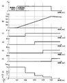
図11及び図12は、いずれも第5の実施の形態にかかる周波数指令修正回路2の動作を例示する波形図である。但し図11で例示される場合の方が、図12で例示される場合よりも、電力変換装置5の動作の不安定性が顕著である。
図11、図12のそれぞれにおいて、(a)は安定判定信号Jを、(b)は積分信号SJを、(c),(d),(e),(f)はそれぞれ修正要求信号K1,K2,K3,K4を、(g)は改周波数指令f**を、それぞれ示す。但し、(c)~(f)において、修正要求信号K1,K2,K3,K4の活性/非活性はそれぞれ整数値1/0で示す。
図11の例示では、時刻t21以前には電力変換装置5の動作が安定であると判定され、安定判定信号Jが“L”となっている。ここでは時刻t21において既に、積分器260の積分についての時定数よりも十分に長い間、電力変換装置5の動作が安定し続けている場合を想定しており、積分信号SJは値0を採る。よって修正要求信号K1,K2,K3,K4は非活性であり、改周波数指令f**は周波数指令f*と等しい値f*を採る。
そして時刻t21において電力変換装置5の動作が不安定であると判定され、安定判定信号Jが“H”となると、積分信号SJは上昇する。時刻t22において積分信号SJが閾値TH1に到達し、修正要求信号K1が活性化し、改周波数指令f**は値f*/2を採る。
更に時刻t22以降においても安定判定信号Jが“H”を維持して積分信号SJは上昇し続け、時刻t23において積分信号SJが閾値TH2に到達し、修正要求信号K2も活性化し、改周波数指令f**は値f*/4を採る。
更に時刻t23以降においても安定判定信号Jが“H”を維持して積分信号SJは上昇し続け、時刻t24において積分信号SJが閾値TH3に到達し、修正要求信号K3も活性化し、改周波数指令f**は値f*/8を採る。
更に時刻t24以降においても安定判定信号Jが“H”を維持して積分信号SJは上昇し続け、時刻t25において積分信号SJが閾値TH4に到達し、修正要求信号K4も活性化し、改周波数指令f**は値0を採る。
改周波数指令f**は値0を採ると、交流回転機11の損失を無視すれば、インバータ1が出力する電力は0となるので電力変換装置5の動作は安定する。よって時刻t25以降では安定判定信号Jは非活性となり、積分信号SJは低下して行く。
図12の例示では、時刻t31以前には電力変換装置5の動作が安定であると判定され、積分信号SJは値0を採る。よって修正要求信号K1,K2,K3,K4は非活性であり、改周波数指令f**は周波数指令f*と等しい値f*を採る。
そして時刻t31において電力変換装置5の動作が不安定であると判定され、安定判定信号Jが“H”となると、積分信号SJは上昇する。時刻t32において積分信号SJが閾値TH1に到達し、修正要求信号K1が活性化し、改周波数指令f**は値f*/2を採る。
更に時刻t32以降においても安定判定信号Jが“H”を維持して積分信号SJは上昇し続け、時刻t33において積分信号SJが閾値TH2に到達し、修正要求信号K2も活性化し、改周波数指令f**は値f*/4を採る。
その後、時刻t33以降においても安定判定信号Jが“H”を維持して積分信号SJは上昇し続けるものの閾値TH3には到達せず、時刻t34において安定判定信号Jが“L”を採り、積分信号SJは低下する。
そして時刻t34において積分信号SJが閾値TH2を下回り、修正要求信号K2も非活性となり、改周波数指令f**は値f*/2を採る。
更に時刻t35においても安定判定信号Jが“L”を維持して積分信号SJは低下し続け、時刻t36において積分信号SJが閾値TH1を下回り、修正要求信号K1も非活性となり、改周波数指令f**は値f*を採る。
このように、積分信号SJと比較される閾値を複数設け、それぞれの閾値の間隔に対応して改周波数指令f**が採る値を設定することにより、指令値を不要に低下させることなく、電力変換装置5の動作を安定に導くことができる。
もちろん、例えば図12に示されるように改周波数指令f**が値f*/4を採ることによって電力変換装置5の動作が安定しても、図12に示される場合とは異なって改周波数指令f**が値f*/2を採ることによって電力変換装置5の動作が再び不安定となることもあり得る。この場合、改周波数指令f**は値f*/2、f*/4を交互に採ることもあり得る。
しかし第4の実施の形態で説明したように、電力変換装置5の動作が不安定となることによって一旦低下した指令値を、電力変換装置5の動作が安定化した後も維持することにより、電力変換装置5の動作が再び不安定になることを防ぐこともできる。
第6の実施の形態.
図13は、第6の実施の形態にかかる周波数指令修正回路2の構成を例示する回路図である。周波数指令修正回路2は、積分器23と減算器24とを有する。
図13は、第6の実施の形態にかかる周波数指令修正回路2の構成を例示する回路図である。周波数指令修正回路2は、積分器23と減算器24とを有する。
積分器23は安定判定信号Jを入力して積分信号SJを出力する。減算器23は周波数指令f*及び積分信号SJを入力して改周波数指令f**を出力する。つまり、第6の実施の形態では、電力変換装置5の動作が不安定であると判定される(つまり安定判定信号Jが活性化する)期間の長さに応じて増大する積分信号SJを、電力が依存する指令値から減じることになる。
このような減算は、第4の実施の形態や第5の実施の形態で示されるような改周波数指令f**の段階的な切り替わりとは異なる。つまり、電力変換装置5の動作の動作が安定となるのに必要な低減量で改周波数指令f**を得ることができるので、改周波数指令f**を過剰に低くすることがない。
図14及び図15は、いずれも第6の実施の形態にかかる周波数指令修正回路2の動作を例示する波形図である。但し図15で例示される場合の方が、図14で例示される場合よりも、電力変換装置5の動作の不安定性が顕著である。
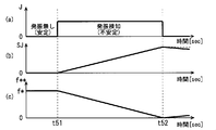
図14,図15のそれぞれにおいて、(a)は安定判定信号Jを、(b)は積分信号SJを、(c)は改周波数指令f**を、それぞれ示す。
図14の例示では、時刻t41以前には電力変換装置5の動作が安定であると判定され、安定判定信号Jが“L”となっている。ここでは時刻t41において既に、積分器23の積分についての時定数よりも十分に長い間、電力変換装置5の動作が安定し続けている場合を想定しており、積分信号SJは値0を採る。よって改周波数指令f**は周波数指令f*と等しい値f*を採る。
そして時刻t41において電力変換装置5の動作が不安定であると判定され、安定判定信号Jが“H”となると、積分信号SJは上昇する。これに伴って改周波数指令f**は低下する。
改周波数指令f**は低下することで、電力変換装置5の動作は安定へと導かれ、時刻t42において電力変換装置5の動作が安定であると判定される。これにより安定判定信号Jが“L”となり、積分信号SJは減少する。これに伴い、改周波数指令f**は上昇する。この後、再び電力変換装置5の動作が不安定であると判定されると改周波数指令f**は減少する。
以上の動作により、電力変換装置5の動作が安定となり得る程度に大きく改周波数指令f**が設定される。
図15の例示では、時刻t51以前には電力変換装置5の動作が安定であると判定され、安定判定信号Jが“L”となっている。ここでは時刻t51において既に、積分器23の積分についての時定数よりも十分に長い間、電力変換装置5の動作が安定し続けている場合を想定しており、積分信号SJは値0を採る。よって改周波数指令f**は周波数指令f*と等しい値f*を採る。
そして時刻t51において電力変換装置5の動作が不安定であると判定され、安定判定信号Jが“H”となると、積分信号SJは上昇する。これに伴って改周波数指令f**は低下する。
更に安定判定信号Jが“H”を維持して積分信号SJは上昇し続け、時刻t52において改周波数指令f**は値0を採る。
改周波数指令f**は値0を採ると、交流回転機11の銅損を無視すれば、インバータ1が出力する電力は0となるので電力変換装置5の動作は安定する。よって時刻t52は以降では安定判定信号Jは非活性となり、積分信号SJは低下し、改周波数指令f**は上昇する。
<変形>
第4の実施の形態及び第5の実施の形態において、改周波数指令f**の低下は、半減することが例示されていたが、これ以外の低下率で低下しても良い。即ち乗算器250,255,256,257の乗数に、値(1/2)以外であって0より大きく1より小さい値を採用することができる。また閾値TH1~TH4はそれらの間の大小関係を損なわなければ、適宜に設定できる。
第4の実施の形態及び第5の実施の形態において、改周波数指令f**の低下は、半減することが例示されていたが、これ以外の低下率で低下しても良い。即ち乗算器250,255,256,257の乗数に、値(1/2)以外であって0より大きく1より小さい値を採用することができる。また閾値TH1~TH4はそれらの間の大小関係を損なわなければ、適宜に設定できる。
第5の実施の形態及び第6の実施の形態において、改周波数指令f**が0となったことを報知してもよい。このような状況では適切に負荷11を駆動することは困難である場合が多いからである。
第6の実施の形態において、改周波数指令f**の低下量は積分信号SJに比例していたが、両者が正の相関関係にあれば、即ち改周波数指令f**と積分信号SJとの間に負の相関関係があればよい。例えば減算器24が、積分信号SJに正の重み付けをして周波数指令f*から差し引いてもよい。
上記変形についても、第4乃至第6の実施の形態と同様に、改周波数指令f**の代わりに改トルク指令T**、改電流指令I**、改電圧指令V**が採用できる。
安定性判定回路6の動作は安定性判定方法として把握することができる。また上述の電力変換装置5はこのような安定性判定方法を採用する点で従来の技術とは明確に相違する。
あるいは、コンバータ8、インバータ1、直流母線70,71、コンデンサ72の他、安定性判定回路6を含めて電力変換装置として把握することもできる。かかる構成に対して更に修正回路2をも含めて、電力変換装置として把握することもできる。
この発明は詳細に説明されたが、上記した説明は、すべての局面において、例示であって、この発明がそれに限定されるものではない。例示されていない無数の変形例が、この発明の範囲から外れることなく想定され得るものと解される。
Claims (13)
- コンバータ(8)と、インバータ(1)と、前記コンバータと前記インバータとを接続する一対の直流母線(70,71)と、前記一対の直流母線の間に接続されるコンデンサ(72)とを備える電力変換装置(5)における動作の安定性を判定する方法であって、
前記一対の直流母線の間の直流電圧(Vdc)の脈動分(Vdcr)の振幅(|Vdcr|)が、所定値(Q)を超えることを以て、前記電力変換装置の動作が不安定であると判定する、安定性判定方法。 - 前記所定値(Q)は、前記平均値(Vdcb)の増加に対して非増加となる値に設定される、請求項1記載の安定性判定方法。
- 前記一対の直流母線の一方(71)において、前記コンバータ(8)と前記インバータ(1)との間に、並列接続体が介在し、
前記並列接続体は、
前記コンデンサ(72)と共にローパスフィルタを形成するインダクタ(3)と、
前記インダクタと並列に接続された可変抵抗(4)と
を有し、
前記電力変換装置の動作が不安定であると判定された場合、前記可変抵抗の抵抗値を低減する、請求項1又は請求項2のいずれか一つに記載の安定性判定方法。 - 前記電力変換装置の動作が不安定であると判定された場合、前記インバータから出力される電力を低減する、請求項1又は請求項2のいずれか一つに記載の安定性判定方法。
- 前記電力変換装置の動作が不安定であると判定された期間の長さに対応して増大する信号(SJ)が所定の閾値(TH0,TH1,TH2,TH3,TH4)を超えることに対応して、前記電力を低減する、請求項4記載の安定性判定方法。
- 前記電力変換装置の動作が不安定であると判定された期間の長さに対応して増大する信号(SJ)を、前記電力が依存する指令値(f*,T*,I*,V*)から減じる、請求項4記載の安定性判定方法。
- コンバータ(8)と、インバータ(1)と、前記コンバータと前記インバータとを接続する一対の直流母線と、前記一対の直流母線の間に接続されるコンデンサ(72)とを備える電力変換装置における動作の安定性を判定する回路であって、
前記一対の直流母線の間の直流電圧の平均値(Vdcb)を得る平均値取得回路(12)と、
前記直流電圧から前記平均値を差し引いて前記直流電圧の脈動分(Vdcr)を得る減算器(13)と、
前記脈動分の振幅(|Vdcr|)を求める絶対値取得回路(15)と、
所定値(Q)を設定する所定値設定器(14)と、
前記所定値と前記振幅とを比較する比較器(16)と
を備える安定性判定回路(6)。 - 前記所定値(Q)は、前記平均値(Vdcb)の増加に対して非増加となる値に設定される、請求項7記載の安定性判定回路(6)。
- コンバータ(8)と、
インバータ(1)と、
前記コンバータと前記インバータとを接続する一対の直流母線(70,71)と、
前記一対の直流母線の間に接続されるコンデンサ(72)と
を備える電力変換装置であって、
前記一対の直流母線の一方において、前記コンバータ(8)と前記インバータ(1)との間に介在する並列接続体
を更に備え、
前記並列接続体は、
前記コンデンサ(72)と共にローパスフィルタを形成するインダクタ(3)と、
前記インダクタと並列に接続された可変抵抗(4)と
を有し、
請求項1又は請求項2のいずれか一つに記載の安定性判定方法によって、前記電力変換装置の動作が不安定であると判定された場合、前記可変抵抗の抵抗値が低減する、電力変換装置(5)。 - コンバータ(8)と、
インバータ(1)と、
前記コンバータと前記インバータとを接続する一対の直流母線(70,71)と、
前記一対の直流母線の間に接続されるコンデンサ(72)と、
安定性判定回路(6)と、
修正回路(2)と
を備え、
前記安定性判定回路は、
前記一対の直流母線の間の直流電圧の平均値(Vdcb)を得る平均値取得回路(12)と、
前記直流電圧から前記平均値を差し引いて前記直流電圧の脈動分(Vdcr)を得る減算器(13)と、
前記脈動分の振幅(|Vdcr|)を求める絶対値取得回路(15)と、
所定値(Q)を設定する所定値設定器(14)と
を有し、
前記修正回路(2)は、前記振幅が前記所定値よりも大きい場合、前記インバータの出力する電力が依存する指令値(f*,T*,I*,V*)を小さく修正して前記インバータに出力する、電力変換装置。 - 前記所定値(Q)は、前記平均値(Vdcb)の増加に対して非増加となる値に設定される、請求項10記載の電力変換装置。
- 前記振幅が前記所定値よりも大きい期間の長さに対応して増大する信号(SJ)が所定の閾値(TH0,TH1,TH2,TH3,TH4)を超えることに対応して、前記指令値(f*,T*,I*,V*)を小さく修正する、請求項10記載の電力変換装置。
- 前記振幅が前記所定値よりも大きい期間の長さに対応して増大する信号(SJ)を、前記指令値(f*,T*,I*,V*)から減じる、請求項10記載の電力変換装置。
Applications Claiming Priority (2)
| Application Number | Priority Date | Filing Date | Title |
|---|---|---|---|
| JP2011-126020 | 2011-06-06 | ||
| JP2011126020 | 2011-06-06 |
Publications (1)
| Publication Number | Publication Date |
|---|---|
| WO2012169269A1 true WO2012169269A1 (ja) | 2012-12-13 |
Family
ID=47295842
Family Applications (1)
| Application Number | Title | Priority Date | Filing Date |
|---|---|---|---|
| PCT/JP2012/058958 Ceased WO2012169269A1 (ja) | 2011-06-06 | 2012-04-02 | 安定性判定方法、安定性判定回路、電力変換装置 |
Country Status (2)
| Country | Link |
|---|---|
| JP (2) | JP2013017375A (ja) |
| WO (1) | WO2012169269A1 (ja) |
Families Citing this family (2)
| Publication number | Priority date | Publication date | Assignee | Title |
|---|---|---|---|---|
| JP6003169B2 (ja) * | 2012-04-12 | 2016-10-05 | ダイキン工業株式会社 | 制御方法、制御装置 |
| WO2020263289A1 (en) * | 2019-06-24 | 2020-12-30 | General Electric Company | Circuit and method for bus voltage variation in power converters |
Citations (2)
| Publication number | Priority date | Publication date | Assignee | Title |
|---|---|---|---|---|
| JP2002247859A (ja) * | 2001-02-16 | 2002-08-30 | Sanken Electric Co Ltd | インバータ装置 |
| JP2004104976A (ja) * | 2002-09-12 | 2004-04-02 | Toshiba Corp | 電力変換装置 |
Family Cites Families (4)
| Publication number | Priority date | Publication date | Assignee | Title |
|---|---|---|---|---|
| JPH033670A (ja) * | 1989-05-26 | 1991-01-09 | Fuji Electric Co Ltd | 誘導加熱用インバータ装置の制御方法 |
| JP4750553B2 (ja) * | 2005-12-28 | 2011-08-17 | 東芝シュネデール・インバータ株式会社 | 電動機制御装置 |
| JP5164138B2 (ja) * | 2007-07-04 | 2013-03-13 | 東芝シュネデール・インバータ株式会社 | 電動機制御装置 |
| JP5194815B2 (ja) * | 2008-01-16 | 2013-05-08 | 株式会社富士通ゼネラル | 平滑コンデンサの異常検出回路及びこれを備えた電子機器 |
-
2012
- 2012-03-23 JP JP2012067347A patent/JP2013017375A/ja active Pending
- 2012-04-02 WO PCT/JP2012/058958 patent/WO2012169269A1/ja not_active Ceased
- 2012-09-03 JP JP2012192838A patent/JP5477435B2/ja not_active Expired - Fee Related
Patent Citations (2)
| Publication number | Priority date | Publication date | Assignee | Title |
|---|---|---|---|---|
| JP2002247859A (ja) * | 2001-02-16 | 2002-08-30 | Sanken Electric Co Ltd | インバータ装置 |
| JP2004104976A (ja) * | 2002-09-12 | 2004-04-02 | Toshiba Corp | 電力変換装置 |
Also Published As
| Publication number | Publication date |
|---|---|
| JP2013017390A (ja) | 2013-01-24 |
| JP5477435B2 (ja) | 2014-04-23 |
| JP2013017375A (ja) | 2013-01-24 |
Similar Documents
| Publication | Publication Date | Title |
|---|---|---|
| JP6295782B2 (ja) | 電力変換装置、発電システム、制御装置および電力変換方法 | |
| JP5817947B1 (ja) | 電力変換制御装置 | |
| CN105356468B (zh) | 无电解电容电机驱动系统及其谐波电流抑制方法和装置 | |
| JP5259077B2 (ja) | 瞬時電圧低下補償回路、電力変換装置、瞬時電圧低下補償方法及び瞬時電圧低下補償プログラム | |
| JP5742980B1 (ja) | 電力変換装置の制御方法 | |
| CN109874373B (zh) | 有源滤波器的控制装置 | |
| WO2015045425A1 (ja) | 電力変換装置 | |
| JP2006271083A (ja) | 電動機制御装置 | |
| JP2016119835A (ja) | 充放電回路、充放電回路の制御方法、充放電回路の制御装置、及び直接形電力変換器 | |
| JP2012151969A (ja) | 電力変換装置 | |
| CN106068604B (zh) | 电力转换装置 | |
| WO2016059969A1 (ja) | アクティブフィルタ、交直変換装置 | |
| JP4909857B2 (ja) | コンバータ装置 | |
| JP2019158456A (ja) | 正弦波フィルタのコンデンサ容量判定装置 | |
| CN107710588B (zh) | 转换设备以及对其进行控制的方法 | |
| JP2019198170A (ja) | 電力変換装置 | |
| TWI641205B (zh) | 漣波補償控制方法與應用此漣波補償控制之電能轉換裝置 | |
| JP5477435B2 (ja) | 安定性判定方法、電力変換装置 | |
| JP6003169B2 (ja) | 制御方法、制御装置 | |
| CN107834827B (zh) | 用于整流器的谐波电流补偿装置 | |
| WO2019097835A1 (ja) | 電力変換装置 | |
| JP5923873B2 (ja) | インバータ制御回路 | |
| JP7602166B1 (ja) | 電力変換装置 | |
| CN106160433B (zh) | 一种用于控制变流器的反馈系统和储能系统 | |
| JP7776779B1 (ja) | モータ制御装置 |
Legal Events
| Date | Code | Title | Description |
|---|---|---|---|
| 121 | Ep: the epo has been informed by wipo that ep was designated in this application |
Ref document number: 12796015 Country of ref document: EP Kind code of ref document: A1 |
|
| NENP | Non-entry into the national phase |
Ref country code: DE |
|
| 122 | Ep: pct application non-entry in european phase |
Ref document number: 12796015 Country of ref document: EP Kind code of ref document: A1 |