WO2012169194A1 - 抵抗変化素子の製造方法およびその製造装置 - Google Patents
抵抗変化素子の製造方法およびその製造装置 Download PDFInfo
- Publication number
- WO2012169194A1 WO2012169194A1 PCT/JP2012/003725 JP2012003725W WO2012169194A1 WO 2012169194 A1 WO2012169194 A1 WO 2012169194A1 JP 2012003725 W JP2012003725 W JP 2012003725W WO 2012169194 A1 WO2012169194 A1 WO 2012169194A1
- Authority
- WO
- WIPO (PCT)
- Prior art keywords
- metal oxide
- target
- oxide layer
- sputtering
- power
- Prior art date
- Legal status (The legal status is an assumption and is not a legal conclusion. Google has not performed a legal analysis and makes no representation as to the accuracy of the status listed.)
- Ceased
Links
Images




Classifications
-
- H—ELECTRICITY
- H10—SEMICONDUCTOR DEVICES; ELECTRIC SOLID-STATE DEVICES NOT OTHERWISE PROVIDED FOR
- H10N—ELECTRIC SOLID-STATE DEVICES NOT OTHERWISE PROVIDED FOR
- H10N70/00—Solid-state devices having no potential barriers, and specially adapted for rectifying, amplifying, oscillating or switching
- H10N70/011—Manufacture or treatment of multistable switching devices
- H10N70/021—Formation of switching materials, e.g. deposition of layers
- H10N70/026—Formation of switching materials, e.g. deposition of layers by physical vapor deposition, e.g. sputtering
-
- C—CHEMISTRY; METALLURGY
- C23—COATING METALLIC MATERIAL; COATING MATERIAL WITH METALLIC MATERIAL; CHEMICAL SURFACE TREATMENT; DIFFUSION TREATMENT OF METALLIC MATERIAL; COATING BY VACUUM EVAPORATION, BY SPUTTERING, BY ION IMPLANTATION OR BY CHEMICAL VAPOUR DEPOSITION, IN GENERAL; INHIBITING CORROSION OF METALLIC MATERIAL OR INCRUSTATION IN GENERAL
- C23C—COATING METALLIC MATERIAL; COATING MATERIAL WITH METALLIC MATERIAL; SURFACE TREATMENT OF METALLIC MATERIAL BY DIFFUSION INTO THE SURFACE, BY CHEMICAL CONVERSION OR SUBSTITUTION; COATING BY VACUUM EVAPORATION, BY SPUTTERING, BY ION IMPLANTATION OR BY CHEMICAL VAPOUR DEPOSITION, IN GENERAL
- C23C14/00—Coating by vacuum evaporation, by sputtering or by ion implantation of the coating forming material
- C23C14/06—Coating by vacuum evaporation, by sputtering or by ion implantation of the coating forming material characterised by the coating material
- C23C14/08—Oxides
-
- C—CHEMISTRY; METALLURGY
- C23—COATING METALLIC MATERIAL; COATING MATERIAL WITH METALLIC MATERIAL; CHEMICAL SURFACE TREATMENT; DIFFUSION TREATMENT OF METALLIC MATERIAL; COATING BY VACUUM EVAPORATION, BY SPUTTERING, BY ION IMPLANTATION OR BY CHEMICAL VAPOUR DEPOSITION, IN GENERAL; INHIBITING CORROSION OF METALLIC MATERIAL OR INCRUSTATION IN GENERAL
- C23C—COATING METALLIC MATERIAL; COATING MATERIAL WITH METALLIC MATERIAL; SURFACE TREATMENT OF METALLIC MATERIAL BY DIFFUSION INTO THE SURFACE, BY CHEMICAL CONVERSION OR SUBSTITUTION; COATING BY VACUUM EVAPORATION, BY SPUTTERING, BY ION IMPLANTATION OR BY CHEMICAL VAPOUR DEPOSITION, IN GENERAL
- C23C14/00—Coating by vacuum evaporation, by sputtering or by ion implantation of the coating forming material
- C23C14/22—Coating by vacuum evaporation, by sputtering or by ion implantation of the coating forming material characterised by the process of coating
- C23C14/34—Sputtering
- C23C14/3464—Sputtering using more than one target
-
- C—CHEMISTRY; METALLURGY
- C23—COATING METALLIC MATERIAL; COATING MATERIAL WITH METALLIC MATERIAL; CHEMICAL SURFACE TREATMENT; DIFFUSION TREATMENT OF METALLIC MATERIAL; COATING BY VACUUM EVAPORATION, BY SPUTTERING, BY ION IMPLANTATION OR BY CHEMICAL VAPOUR DEPOSITION, IN GENERAL; INHIBITING CORROSION OF METALLIC MATERIAL OR INCRUSTATION IN GENERAL
- C23C—COATING METALLIC MATERIAL; COATING MATERIAL WITH METALLIC MATERIAL; SURFACE TREATMENT OF METALLIC MATERIAL BY DIFFUSION INTO THE SURFACE, BY CHEMICAL CONVERSION OR SUBSTITUTION; COATING BY VACUUM EVAPORATION, BY SPUTTERING, BY ION IMPLANTATION OR BY CHEMICAL VAPOUR DEPOSITION, IN GENERAL
- C23C14/00—Coating by vacuum evaporation, by sputtering or by ion implantation of the coating forming material
- C23C14/22—Coating by vacuum evaporation, by sputtering or by ion implantation of the coating forming material characterised by the process of coating
- C23C14/34—Sputtering
- C23C14/3492—Variation of parameters during sputtering
-
- C—CHEMISTRY; METALLURGY
- C23—COATING METALLIC MATERIAL; COATING MATERIAL WITH METALLIC MATERIAL; CHEMICAL SURFACE TREATMENT; DIFFUSION TREATMENT OF METALLIC MATERIAL; COATING BY VACUUM EVAPORATION, BY SPUTTERING, BY ION IMPLANTATION OR BY CHEMICAL VAPOUR DEPOSITION, IN GENERAL; INHIBITING CORROSION OF METALLIC MATERIAL OR INCRUSTATION IN GENERAL
- C23C—COATING METALLIC MATERIAL; COATING MATERIAL WITH METALLIC MATERIAL; SURFACE TREATMENT OF METALLIC MATERIAL BY DIFFUSION INTO THE SURFACE, BY CHEMICAL CONVERSION OR SUBSTITUTION; COATING BY VACUUM EVAPORATION, BY SPUTTERING, BY ION IMPLANTATION OR BY CHEMICAL VAPOUR DEPOSITION, IN GENERAL
- C23C14/00—Coating by vacuum evaporation, by sputtering or by ion implantation of the coating forming material
- C23C14/22—Coating by vacuum evaporation, by sputtering or by ion implantation of the coating forming material characterised by the process of coating
- C23C14/54—Controlling or regulating the coating process
- C23C14/542—Controlling the film thickness or evaporation rate
-
- C—CHEMISTRY; METALLURGY
- C23—COATING METALLIC MATERIAL; COATING MATERIAL WITH METALLIC MATERIAL; CHEMICAL SURFACE TREATMENT; DIFFUSION TREATMENT OF METALLIC MATERIAL; COATING BY VACUUM EVAPORATION, BY SPUTTERING, BY ION IMPLANTATION OR BY CHEMICAL VAPOUR DEPOSITION, IN GENERAL; INHIBITING CORROSION OF METALLIC MATERIAL OR INCRUSTATION IN GENERAL
- C23C—COATING METALLIC MATERIAL; COATING MATERIAL WITH METALLIC MATERIAL; SURFACE TREATMENT OF METALLIC MATERIAL BY DIFFUSION INTO THE SURFACE, BY CHEMICAL CONVERSION OR SUBSTITUTION; COATING BY VACUUM EVAPORATION, BY SPUTTERING, BY ION IMPLANTATION OR BY CHEMICAL VAPOUR DEPOSITION, IN GENERAL
- C23C14/00—Coating by vacuum evaporation, by sputtering or by ion implantation of the coating forming material
- C23C14/22—Coating by vacuum evaporation, by sputtering or by ion implantation of the coating forming material characterised by the process of coating
- C23C14/54—Controlling or regulating the coating process
- C23C14/548—Controlling the composition
-
- H—ELECTRICITY
- H01—ELECTRIC ELEMENTS
- H01J—ELECTRIC DISCHARGE TUBES OR DISCHARGE LAMPS
- H01J37/00—Discharge tubes with provision for introducing objects or material to be exposed to the discharge, e.g. for the purpose of examination or processing thereof
- H01J37/32—Gas-filled discharge tubes
- H01J37/34—Gas-filled discharge tubes operating with cathodic sputtering
-
- H—ELECTRICITY
- H01—ELECTRIC ELEMENTS
- H01J—ELECTRIC DISCHARGE TUBES OR DISCHARGE LAMPS
- H01J37/00—Discharge tubes with provision for introducing objects or material to be exposed to the discharge, e.g. for the purpose of examination or processing thereof
- H01J37/32—Gas-filled discharge tubes
- H01J37/34—Gas-filled discharge tubes operating with cathodic sputtering
- H01J37/3411—Constructional aspects of the reactor
- H01J37/3414—Targets
- H01J37/3426—Material
-
- H—ELECTRICITY
- H01—ELECTRIC ELEMENTS
- H01J—ELECTRIC DISCHARGE TUBES OR DISCHARGE LAMPS
- H01J37/00—Discharge tubes with provision for introducing objects or material to be exposed to the discharge, e.g. for the purpose of examination or processing thereof
- H01J37/32—Gas-filled discharge tubes
- H01J37/34—Gas-filled discharge tubes operating with cathodic sputtering
- H01J37/3411—Constructional aspects of the reactor
- H01J37/3414—Targets
- H01J37/3426—Material
- H01J37/3429—Plural materials
-
- H—ELECTRICITY
- H10—SEMICONDUCTOR DEVICES; ELECTRIC SOLID-STATE DEVICES NOT OTHERWISE PROVIDED FOR
- H10B—ELECTRONIC MEMORY DEVICES
- H10B63/00—Resistance change memory devices, e.g. resistive RAM [ReRAM] devices
-
- H—ELECTRICITY
- H10—SEMICONDUCTOR DEVICES; ELECTRIC SOLID-STATE DEVICES NOT OTHERWISE PROVIDED FOR
- H10N—ELECTRIC SOLID-STATE DEVICES NOT OTHERWISE PROVIDED FOR
- H10N70/00—Solid-state devices having no potential barriers, and specially adapted for rectifying, amplifying, oscillating or switching
- H10N70/20—Multistable switching devices, e.g. memristors
-
- H—ELECTRICITY
- H10—SEMICONDUCTOR DEVICES; ELECTRIC SOLID-STATE DEVICES NOT OTHERWISE PROVIDED FOR
- H10N—ELECTRIC SOLID-STATE DEVICES NOT OTHERWISE PROVIDED FOR
- H10N70/00—Solid-state devices having no potential barriers, and specially adapted for rectifying, amplifying, oscillating or switching
- H10N70/801—Constructional details of multistable switching devices
- H10N70/881—Switching materials
- H10N70/883—Oxides or nitrides
- H10N70/8833—Binary metal oxides, e.g. TaOx
-
- H—ELECTRICITY
- H10—SEMICONDUCTOR DEVICES; ELECTRIC SOLID-STATE DEVICES NOT OTHERWISE PROVIDED FOR
- H10P—GENERIC PROCESSES OR APPARATUS FOR THE MANUFACTURE OR TREATMENT OF DEVICES COVERED BY CLASS H10
- H10P14/00—Formation of materials, e.g. in the shape of layers or pillars
- H10P14/20—Formation of materials, e.g. in the shape of layers or pillars of semiconductor materials
- H10P14/22—Formation of materials, e.g. in the shape of layers or pillars of semiconductor materials using physical deposition, e.g. vacuum deposition or sputtering
Definitions
- the present invention relates to a manufacturing method and a manufacturing apparatus for a resistance change element used as a nonvolatile memory or the like.
- Semiconductor memory includes volatile memory such as DRAM (Dynamic Random Access Memory) and nonvolatile memory such as flash memory.
- volatile memory such as DRAM (Dynamic Random Access Memory)
- nonvolatile memory such as flash memory.
- a NAND flash memory or the like is known as a non-volatile memory, but ReRAM (Resistance RAM) has attracted attention as a device that can be further miniaturized.
- ReRAM uses a variable resistor that changes its resistance value in response to a pulse voltage as a resistance element.
- This variable resistor is typically a metal oxide layer of two or more layers having different degrees of oxidation, that is, resistivity, and has a structure in which these are sandwiched between upper and lower electrodes.
- a method of forming oxide layer structures having different degrees of oxidation a method of forming a metal oxide by so-called reactive sputtering in which a metal target is sputtered in an oxygen atmosphere is known.
- Patent Document 1 discloses an n-type transition metal oxide layer having a high oxygen concentration and a p-type transition metal oxide layer having a low oxygen concentration by reducing the supply amount of oxygen while sputtering a metal target. A method of laminating is described.
- an object of the present invention is to provide a variable resistance element manufacturing method and a manufacturing apparatus capable of accurately forming a metal oxide layer having a desired resistivity.
- a variable resistance element manufacturing method is different from the step of forming a first metal oxide having a first resistivity and the first resistivity.
- Forming a second metal oxide having a second resistivity The first metal oxide is formed on the substrate by sputtering the second target made of the metal with the first power while sputtering the first target made of the metal oxide.
- the second metal oxide layer is formed by sputtering the second target with a second power different from the first power while sputtering the first target. Formed on top.
- the variable resistance element manufacturing apparatus includes a vacuum chamber, a first sputter cathode, a second sputter cathode, and a control unit.
- the first sputter cathode is attached to the vacuum chamber and includes a first target made of a metal oxide.
- the second sputter cathode is attached to the vacuum chamber and includes a second target made of the metal.
- the control unit sputters the first target, sputters the second target with a first power, and sputters the first target while sputtering the second target.
- a switching unit that sequentially switches between a second state of sputtering with a second power different from the first power.
- the method of manufacturing a variable resistance element includes a step of forming a first metal oxide having a first resistivity, and a second resistivity different from the first resistivity. Forming a second metal oxide.
- the first metal oxide is formed on the substrate by sputtering the second target made of the metal with the first power while sputtering the first target made of the metal oxide.
- the second metal oxide layer is formed by sputtering the second target with a second power different from the first power while sputtering the first target. Formed on top.
- variable resistance element manufacturing method a first target made of a metal oxide and a second target made of the metal are simultaneously sputtered to form a film. At this time, the degree of oxidation of the metal oxide layer formed is controlled by changing the target power. Thereby, a metal oxide layer having a desired degree of oxidation, that is, resistivity can be formed with high accuracy.
- the first metal oxide layer is formed by sputtering the second target with the first power while sputtering the first target with the third power.
- the second metal oxide layer may be formed by sputtering the second target with the second power while sputtering the first target with the third power.
- the resistivity of the metal oxide layer formed only by the power of the second target can be controlled without changing the power of the first target.
- the first metal oxide layer and the second metal oxide layer may both be formed by sputtering using a rare gas. As a result, the influence of the gas contributing to plasma formation can be reduced, and the resistivity of the metal oxide layer can be controlled more accurately.
- the oxide material that constitutes the first target and the metal material that constitutes the second target are not particularly limited.
- the first target is made of tantalum oxide
- the second target is made of tantalum. Become.
- the variable resistance element manufacturing apparatus includes a vacuum chamber, a first sputter cathode, a second sputter cathode, and a control unit.
- the first sputter cathode is attached to the vacuum chamber and includes a first target made of a metal oxide.
- the second sputter cathode is attached to the vacuum chamber and includes a second target made of the metal.
- the control unit sputters the first target, sputters the second target with a first power, and sputters the first target while sputtering the second target.
- a switching unit that sequentially switches between a second state of sputtering with a second power different from the first power.
- the control unit according to the resistance change element manufacturing apparatus includes a switching unit that sequentially switches between the first state and the second state in which the sputtering power of the second target is different. Since the resistivity of the metal oxide layer can be accurately controlled by the sputtering power of the second target, a stacked structure of metal oxides having different resistivity can be formed.
- FIG. 1 is a sectional view showing a resistance change element manufacturing apparatus according to an embodiment of the present invention.
- the manufacturing apparatus is configured by a sputtering apparatus.
- the sputtering apparatus 10 includes a vacuum chamber 11, a sputtering cathode 12 ⁇ / b> A attached to the vacuum chamber 11, a sputtering cathode 12 ⁇ / b> B, and a controller 13.
- the vacuum chamber 11 defines a processing chamber C therein, and the soot processing chamber C can be depressurized to a predetermined degree of vacuum through a vacuum exhaust unit (not shown).
- a gas introduction pipe 19 for introducing argon (Ar) gas into the processing chamber C is attached from the peripheral edge of the vacuum chamber 11 into the processing chamber C.
- the substrate support 14 is installed at the approximate center in the vacuum chamber 11, and an electrostatic chuck electrode 141 is installed therein as appropriate. Thereby, the wafer W can be adhered to the surface of the substrate support 14. Further, an adhesion preventing plate 17 is disposed around the substrate support 14 to suppress the sputtered sputter particles from adhering to the inner wall of the vacuum chamber 11.
- the substrate support 14 is installed on the base 15.
- the pedestal 15 has a rotating shaft 15L attached to the center of the lower surface thereof, and is configured to be rotatable via a drive source (not shown) such as a motor. Thereby, a substrate rotating mechanism for rotating the wafer W around its center is configured.
- the rotating shaft 15L is attached to the vacuum chamber 11 via a seal mechanism 151 such as a bearing mechanism (not shown) or a magnetic fluid seal.
- the sputter cathode 12 ⁇ / b> A and the sputter cathode 12 ⁇ / b> B are attached to the upper portion of the vacuum chamber 11 so as to be inclined by a predetermined angle so that the sputtered particles are incident obliquely with respect to the normal direction of the wafer W.
- a target T1 and a target T2 are disposed on the sputtering cathode 12A and the sputtering cathode 12B so as to face the processing chamber C, respectively.
- the sputtering cathodes 12A and 12B are provided with a backing plate that supports the targets T1 and T2 in a coolable manner, a magnetic circuit that forms a magnetic field on the surfaces of the targets T1 and T2, and the like.
- the target T1 is made of an oxide material such as tantalum oxide (TaO X ).
- TaO X tantalum oxide
- Binary oxides of transition metals such as X 2 and CuO X can be used.
- the target T2 is made of a metal material such as tantalum (Ta).
- the constituent material of the target T2 is not limited to this, and the transition metal used for the target T1 can be used.
- the number of sputter cathodes is not limited to two and may be three or more.
- the plurality of sputter cathodes are not limited to the examples used at the same time, and may be used alone.
- a shutter mechanism 16 for selecting a target to be used for film formation is provided in the processing chamber C.
- the shutter mechanism 16 includes, for example, a plurality of shielding plates 161 and a rotating shaft 162 that individually rotates these shielding plates 161.
- Each shielding plate 161 is made of, for example, an umbrella-shaped metal plate having a size capable of covering all the sputtering cathodes, and an opening is formed in advance at a corresponding portion of each sputtering cathode. Then, the rotation shaft 162 is driven to appropriately adjust the rotation position of the 161 so that any one or more sputter targets to be opened can be selected.
- the number of shielding plates 161 is not limited to the illustrated example.
- the target T1 is connected to an RF power source 18A installed outside the vacuum chamber 11.
- the RF power source 18A has a frequency of 13.56 MHz and a power of 500 W.
- the target T2 is connected to a variable power source 18B installed outside the vacuum chamber 11.
- the variable power source 18B is composed of a variable DC power source.
- the variable power range of the variable power source 18B is, for example, 10 to 450W.
- the controller 13 (control unit) is typically configured by a computer, and the entire operation of the sputtering apparatus 10, that is, the evacuation means, the gas flow rate, the electrostatic chuck electrode 141, the RF power source 18A, and the variable power source 18B. Control etc.
- the controller 13 is installed outside the vacuum chamber 11.
- the controller 13 sputters the target T1 while sputtering the target T2 with the first power P1, and the controller 13 sputters the first target T1 while sputtering the target T2 with the second power P2.
- the state of 2 is sequentially switched.
- the variable power source 18B is configured by a variable DC power source, and the variable power source 18B constitutes a switching unit that switches between the first state and the second state.
- the first power P1 is set to a value lower than the second power P2.
- the first power P1 is set to 500 W, for example, and the second power P2 is set to 200 W, for example.
- the sputtering apparatus 10 manufactures a variable resistance element schematically shown in FIG. 2, for example. Next, the configuration of the variable resistance element will be described.
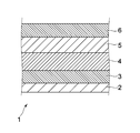
- FIG. 2 is a schematic diagram showing the configuration of the variable resistance element 1 according to this embodiment.
- the resistance change element 1 includes a substrate 2, a lower electrode layer 3, a first metal oxide layer 4, a second metal oxide layer 5, and an upper electrode layer 6.
- the substrate 2 may be a silicon substrate, for example, but the material is not particularly limited.
- the lower electrode layer 3 is formed on the substrate 2 and is made of Ta in this embodiment.
- the material is not limited to this, for example, transition metals such as Hf, Z r, Ti, Al, Fe, Co, M n, Sn, Zn, C r, V, W, or alloys thereof (TaSi, WSi) , Silicon alloys such as TiSi, nitrogen compounds such as TaN, WaN, TiN, and TiAlN, carbon alloys such as TaC, and the like.
- the first metal oxide layer 4 is formed on the lower electrode layer 3 and is made of TaOx in this embodiment.
- TaOx used for the first metal oxide layer 4 is an oxide close to the stoichiometric composition.
- the material is not limited to this, and, for example, ZrOx, HfOx, TiOx, AlOx, SiOx, FeOx, NiOx, CoOx, MnOx, SnOx, ZnOx, VOx, WOx, CuOx and other binary oxides of transition metals Etc. can be used.
- the resistivity of the first metal oxide layer 4 is not limited as long as desired element characteristics can be obtained, but is a value larger than 10 6 ⁇ cm, for example.
- the second metal oxide layer 5 is formed on the first metal oxide layer 4 and is formed of TaOx in this embodiment.
- TaOx used for the second metal oxide layer 5 is an oxide having a lower degree of oxidation than TaOx forming the first metal oxide layer 4 and containing many oxygen vacancies.
- the material is not limited to this, and, for example, ZrOx, HfOx, TiOx, AlOx, SiOx, FeOx, NiOx, CoOx, MnOx, SnOx, ZnOx, VOx, WOx, CuOx and other binary oxides of transition metals Etc. can be used.
- the same oxide as the first metal oxide layer 4 or a different oxide may be used.
- the resistivity of the second metal oxide layer 5 only needs to be smaller than the resistivity of the first metal oxide layer 4, and is, for example, greater than 1 ⁇ cm and 10 6 ⁇ cm or less.
- the upper electrode layer 6 is formed on the second metal oxide layer 5 and is made of Ta in this embodiment.
- the material is not limited to this, for example, transition metals such as Hf, Z r, Ti, Al, Fe, C o, M n, Sn, Zn, Cr, V, W, or alloys thereof (TaSi, WSi) , Silicon alloys such as TiSi, nitrogen compounds such as TaN, WaN, TiN, and TiAlN, and carbon alloys such as TaC).
- the first metal oxide layer 4 of the resistance change element 1 has a higher degree of oxidation than the second metal oxide layer 5, it has a higher resistivity than the second metal oxide layer.
- oxygen ions (O 2 ⁇ ) in the first metal oxide layer 4 having a high resistance have a low resistance. 2 diffuses into the metal oxide layer 5 and the resistance of the first metal oxide layer 4 decreases (low resistance state).
- O 2 ⁇ diffuses from the second metal oxide layer 5 to the first metal oxide layer 4. This increases the degree of oxidation of the metal oxide layer 4 and increases the resistance (high resistance state).
- the first metal oxide layer 4 reversibly switches between the low resistance state and the high resistance state by controlling the voltage between the lower electrode layer 3 and the upper electrode layer 6. Furthermore, since the low resistance state and the high resistance state are maintained even when no voltage is applied, the resistance change element 1 can be used as a nonvolatile memory element.
- variable resistance element 1 using the sputtering apparatus 10 will be described.
- the manufacturing method of the resistance change element 1 includes the following four steps. That is, the formation process of the lower electrode layer 3, the formation process of the first metal oxide layer 4, the formation process of the second metal oxide layer 5, and the formation process of the upper electrode layer 6. Each will be described below.
- Formation of lower electrode layer As a method for forming the lower electrode layer 3, for example, vapor deposition, a sputtering method, a CVD method, an ALD method, or the like is employed.
- the lower electrode layer 3 is formed by the sputtering apparatus 10. In this case, only the target T2 opened by the shutter mechanism 16 is sputtered.
- the substrate 2 is placed on the substrate support 14 in the processing chamber C that has been depressurized to a predetermined degree of vacuum, and Ar gas is introduced into the processing chamber C as a sputtering gas. Then, the lower electrode layer 3 having a high film thickness uniformity can be formed on the substrate 2 by sputtering the target T2 while rotating the substrate support 14 at a predetermined rotational speed.
- the supply power of the target T2 at this time is not particularly limited, and is 200 W, for example.
- the first metal oxide layer 4 is formed on the lower electrode layer 3.
- Ar gas is introduced into the processing chamber C from the gas introduction pipe 19 at a predetermined flow rate.
- the shutter mechanism 16 opens the target T1 and the target T2.
- the controller 13 simultaneously sputters the target T1 and the target T2 in the first state. Thereby, the first metal oxide layer 4 having a high film thickness uniformity is formed over the entire surface of the lower electrode layer 3.
- a second metal oxide layer 5 is formed.
- the controller 13 simultaneously sputters the targets T1 and T2 in the second state.
- the second metal oxide layer 5 having high film thickness uniformity is formed over the entire surface of the first metal oxide layer 4.
- the power of the RF power source 18A is kept constant throughout the first metal oxide layer 4 forming step and the second metal oxide layer 5 forming step. That is, by adjusting only the power of the variable power source 18B, the sputtering rate of the target T2 is controlled, and the resistivity of the first metal oxide layer 4 and the second metal oxide layer 5 is controlled. Yes.
- FIG. 3 is a timing chart showing the power change of the variable power source 18B when the first metal oxide layer 4 and the second metal oxide layer 5 are formed.
- the horizontal axis represents time, and the vertical axis represents power value. Indicates.
- the controller 13 sequentially switches the power of the power source 18B from P1 to P2.
- the first metal oxide layer 4 is formed in the period from the start of sputtering to time t1
- the second metal oxide layer 5 is formed in the period from time t1 to time t2.
- Times t1 and t2 are set according to the magnitudes of power P1 and P2, the required film thickness, and the like.
- the upper electrode layer 6 is formed on the second metal oxide layer 5.
- the upper electrode layer 6 can be formed in the same manner as the lower electrode layer 3.
- the upper electrode layer 6 is formed by the sputtering apparatus 10.
- the degree of oxidation of the physical layer 5 is controlled.
- FIG. 4 is an experimental result showing the relationship between the oxygen flow rate and the resistivity of the metal oxide layer when the metal oxide layer is formed by sputtering a Ta target in an oxidizing atmosphere.
- FIG. 4 shows that when the metal oxide layer having a resistivity higher than 1 ⁇ cm is formed, the change in resistivity with respect to the oxygen flow rate becomes very large. This is presumably because when the oxygen flow rate is increased, the oxidation of the target proceeds and the degree of oxidation of the formed metal oxide layer tends to increase. For this reason, in order to form the second metal oxide layer 5 having a resistivity greater than 1 ⁇ cm and equal to or less than 10 6 ⁇ cm, it is necessary to adjust the oxygen flow rate very accurately, which is difficult.
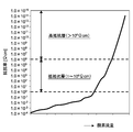
- FIG. 5 is an experimental result showing a change in resistivity of the formed metal oxide layer when the metal target and the metal oxide target are simultaneously sputtered and the power supplied to the metal target is changed. At this time, the power supplied to the metal oxide target was constant, and the sputtering gas was Ar.
- the power supplied to the metal target corresponding to the resistivity of more than 1 ⁇ cm and 10 6 ⁇ cm or less changes gradually. This is presumably because the reactive gas is not used and thus there is little influence from the introduced gas, and stable sputtering is possible. Therefore, also when creating the second metal oxide layer 5 according to the present embodiment, the resistivity can be accurately controlled by adjusting only the power of the variable power source 18B.
- the resistivity distribution is likely to occur in the wafer surface or between the wafers due to oxidation on the target surface or the surface of the adhesion prevention plate, and it is difficult to control the distribution.
- an example in which the metal oxide layer is formed using the method according to the present embodiment is compared with an example in which the metal oxide layer is formed by controlling the resistivity by adjusting the oxygen flow rate. Will be further described.
- FIGS. 6A and 6B are experimental results showing the in-wafer distribution of the resistivity of the metal oxide layer.
- FIGS. 7A and 7B show the resistivity of the metal oxide layer when a plurality of wafers are continuously sputtered. It is one experimental result which shows distribution between wafers.
- 6A and 7A show the case where the resistivity is controlled by adjusting the oxygen flow rate
- FIGS. 6B and 7B show the case where the resistivity is controlled by the method according to the present embodiment, that is, by controlling the power supplied to the metal target. ing. In the experiment, a 12-inch wafer was used.
- FIG. 6A shows a distribution in the wafer where the resistivity is low near the center of the wafer and the resistivity is high as the distance from the center increases.
- the resistivity distribution within the wafer surface is ⁇ 65%. This is considered to be because oxygen gas reacts on the surface of the deposition plate located around the substrate support and the peripheral edge of the wafer, and the amount of oxygen gas reacting with the sputtered particles decreases in the center of the wafer. .
- the resistivity shows a uniform distribution in the wafer and is within a range of ⁇ 2%. This is presumably because a reactive gas is not used for sputtering, so that the influence of the introduced gas is small and a metal oxide layer having a uniform oxidation degree can be formed.
- the resistivity increases as the number of continuously sputtered wafers increases, and the resistivity distribution between the wafers is ⁇ 42.9%. This is presumably because the oxidation of the metal target proceeds with oxygen gas as the time for sputtering elapses, and the degree of oxidation of the sputtered particles increases, resulting in an increase in the degree of oxidation of the formed metal oxide layer.
- the resistivity distribution between the wafers is ⁇ 4.5%, indicating a substantially uniform distribution. This is presumably because the reactive gas is not used for sputtering, so that the change in target composition over time is small and sputtering can be performed stably. From this, in this embodiment, even when a plurality of metal oxide layers are continuously formed, it is possible to accurately control the resistivity between wafers.
- a metal oxide layer having a desired degree of oxidation that is, a resistivity can be formed with high accuracy, so that a variable resistance element having desired electrical characteristics can be stably formed. Can be manufactured.
- the power supplied to the target T2 is controlled, but the power supplied to the target T1 may be controlled as necessary.
- variable resistance element in which the first metal oxide layer 4 has a higher resistivity than the second metal oxide layer 5 is manufactured, but instead of this, the second metal oxide layer is formed. It is also possible to produce a resistance change element in which the physical layer 5 has a higher resistivity than the first metal oxide layer 4.
Landscapes
- Chemical & Material Sciences (AREA)
- Engineering & Computer Science (AREA)
- Materials Engineering (AREA)
- Chemical Kinetics & Catalysis (AREA)
- Mechanical Engineering (AREA)
- Metallurgy (AREA)
- Organic Chemistry (AREA)
- Plasma & Fusion (AREA)
- Analytical Chemistry (AREA)
- Physics & Mathematics (AREA)
- Manufacturing & Machinery (AREA)
- Semiconductor Memories (AREA)
- Physical Vapour Deposition (AREA)
Abstract
Description
上記第1の金属酸化物は、金属の酸化物からなる第1のターゲットをスパッタしつつ、上記金属からなる第2のターゲットを第1の電力でスパッタすることで、基板上に形成される。
上記第2の金属酸化物層は、第1のターゲットをスパッタしつつ、上記第2のターゲットを上記第1の電力と異なる第2の電力でスパッタすることで、上記第1の金属酸化物層上に形成される。
上記第1のスパッタカソードは、上記真空チャンバに取り付けられ、金属の酸化物からなる第1のターゲットを含む。
上記第2のスパッタカソードは、上記真空チャンバに取り付けられ、上記金属からなる第2のターゲットを含む。
上記制御ユニットは、上記第1のターゲットをスパッタしつつ、上記第2のターゲットを第1の電力でスパッタする第1の状態と、上記第1のターゲットをスパッタしつつ、上記第2のターゲットを上記第1の電力と異なる第2の電力でスパッタする第2の状態とを順に切り替える切替部を有する。
上記第1の金属酸化物は、金属の酸化物からなる第1のターゲットをスパッタしつつ、上記金属からなる第2のターゲットを第1の電力でスパッタすることで、基板上に形成される。
上記第2の金属酸化物層は、第1のターゲットをスパッタしつつ、上記第2のターゲットを上記第1の電力と異なる第2の電力でスパッタすることで、上記第1の金属酸化物層上に形成される。
上記第2の金属酸化物層は、上記第1のターゲットを上記第3の電力でスパッタしつつ、上記第2のターゲットを上記第2の電力でスパッタすることで形成されてもよい。
これによって、プラズマ形成に寄与するガスによる影響を少なくし、より精度よく金属酸化物層の抵抗率を制御することができる。
上記第1のスパッタカソードは、上記真空チャンバに取り付けられ、金属の酸化物からなる第1のターゲットを含む。
上記第2のスパッタカソードは、上記真空チャンバに取り付けられ、上記金属からなる第2のターゲットを含む。
上記制御ユニットは、上記第1のターゲットをスパッタしつつ、上記第2のターゲットを第1の電力でスパッタする第1の状態と、上記第1のターゲットをスパッタしつつ、上記第2のターゲットを上記第1の電力と異なる第2の電力でスパッタする第2の状態とを順に切り替える切替部を有する。
(抵抗変化素子の製造装置の構成)
図1は、本発明の一実施形態に係る抵抗変化素子の製造装置を示す断面図である。本実施形態では、上記製造装置は、スパッタ装置で構成される。スパッタ装置10は、真空チャンバ11と、真空チャンバ11に取り付けられたスパッタカソード12Aと、スパッタカソード12Bと、コントローラ13とを具備する。
図2は、本実施形態に係る抵抗変化素子1の構成を示した模式図である。抵抗変化素子1は、基板2、下部電極層3、第1の金属酸化物層4、第2の金属酸化物層5、上部電極層6を有する。
抵抗変化素子1の製造方法は、以下の4工程を有する。すなわち、下部電極層3の形成工程、第1の金属酸化物層4の形成工程、第2の金属酸化物層5の形成工程および上部電極層6の形成工程である。以下、それぞれについて説明する。
下部電極層3の形成方法としては、例えば蒸着、スバッタ法、CVD法、ALD法等が採用される。本実施形態では、スパッタ装置10によって下部電極層3が形成される。この場合、シャッタ機構16により開放されたターゲットT2のみがスパッタされる。
次に、下部電極層3の上に、第1の金属酸化物層4が形成される。処理室Cの内部にガス導入配管19よりArガスが所定の流量で導入される。シャッタ機構16は、ターゲットT1及びターゲットT2を開放させる。そして、コントローラ13は、上記第1の状態で、ターゲットT1及びターゲットT2を同時にスパッタする。これにより、下部電極層3の表面全体にわたって膜厚均一性の高い第1の金属酸化物層4が形成される。
続いて、第2の金属酸化物層5を形成する。この工程では、コントローラ13は、上記第2の状態で、ターゲットT1,T2を同時にスパッタする。これにより、第1の金属酸化物層4の表面全体にわたって膜厚均一性の高い第2の金属酸化物層5が形成される。
続いて、第2の金属酸化物層5の上に、上部電極層6が形成される。上部電極層6は、下部電極層3と同様に形成することができ、本実施形態では、スパッタ装置10によって上部電極層6が形成される。
2…基板
3…下部電極層
4…第1の金属酸化物層
5…第2の金属酸化物層
6…上部電極層
10…スパッタ装置
11…真空チャンパ
12A,12B…スパッタカソード
13…コントローラ
14…基板支持台
18A…RF電源
18B…可変電源
T1,T2…ターゲット
Claims (5)
- 金属の酸化物からなる第1のターゲットをスパッタしつつ、前記金属からなる第2のターゲットを第1の電力でスパッタすることで、第1の抵抗率を有する第1の金属酸化物層を基板上に形成し、
前記第1のターゲットをスパッタしつつ、前記第2のターゲットを前記第1の電力と異なる第2の電力でスパッタすることで、前記第1の抵抗率とは異なる第2の抵抗率を有する第2の金属酸化物層を前記第1の金属酸化物層上に形成する
抵抗変化素子の製造方法。 - 請求項1に記載の抵抗変化素子の製造方法であって、
前記第1の金属酸化物層は、前記第1のターゲットを第3の電力でスパッタしつつ、前記第2のターゲットを前記第1の電力でスパッタすることで形成され、
前記第2の金属酸化物層は、前記第1のターゲットを前記第3の電力でスパッタしつつ、前記第2のターゲットを前記第2の電力でスパッタすることで形成される
抵抗変化素子の製造方法。 - 請求項1または2の何れかに記載の抵抗変化素子の製造方法であって、
前記第1の金属酸化物層と前記第2の金属酸化物層とは、いずれも希ガスを用いてスパッタすることで形成される
抵抗変化素子の製造方法。 - 請求項1から3の何れかに記載の抵抗変化素子の製造方法であって、
前記第1のターゲットは、タンタル酸化物からなり、
前記第2のターゲットは、タンタルからなる
抵抗変化素子の製造方法。 - 真空チャンバと、
前記真空チャンバに取り付けられ、金属の酸化物からなる第1のターゲットを含む第1のスパッタカソードと、
前記真空チャンバに取り付けられ、前記金属からなる第2のターゲットを含む第2のスパッタカソードと、
前記第1のターゲットをスパッタしつつ、前記第2のターゲットを第1の電力でスパッタする第1の状態と、前記第1のターゲットをスパッタしつつ、前記第2のターゲットを前記第1の電力と異なる第2の電力でスパッタする第2の状態とを順に切り替える切替部を有する制御ユニットと
を具備する抵抗変化素子の製造装置。
Priority Applications (4)
| Application Number | Priority Date | Filing Date | Title |
|---|---|---|---|
| KR1020137033473A KR20140007493A (ko) | 2011-06-08 | 2012-06-07 | 저항 변화 소자의 제조 방법 및 그 제조 장치 |
| US14/122,966 US9269903B2 (en) | 2011-06-08 | 2012-06-07 | Method of manufacturing variable resistance element and apparatus for manufacturing the same |
| JP2013519388A JP5499220B2 (ja) | 2011-06-08 | 2012-06-07 | 抵抗変化素子の製造方法およびその製造装置 |
| KR1020147021896A KR20140107674A (ko) | 2011-06-08 | 2012-06-07 | 저항 변화 소자의 제조 방법 및 그 제조 장치 |
Applications Claiming Priority (2)
| Application Number | Priority Date | Filing Date | Title |
|---|---|---|---|
| JP2011128169 | 2011-06-08 | ||
| JP2011-128169 | 2011-06-08 |
Publications (1)
| Publication Number | Publication Date |
|---|---|
| WO2012169194A1 true WO2012169194A1 (ja) | 2012-12-13 |
Family
ID=47295777
Family Applications (1)
| Application Number | Title | Priority Date | Filing Date |
|---|---|---|---|
| PCT/JP2012/003725 Ceased WO2012169194A1 (ja) | 2011-06-08 | 2012-06-07 | 抵抗変化素子の製造方法およびその製造装置 |
Country Status (4)
| Country | Link |
|---|---|
| US (1) | US9269903B2 (ja) |
| JP (1) | JP5499220B2 (ja) |
| KR (2) | KR20140007493A (ja) |
| WO (1) | WO2012169194A1 (ja) |
Cited By (1)
| Publication number | Priority date | Publication date | Assignee | Title |
|---|---|---|---|---|
| JP2021136356A (ja) * | 2020-02-27 | 2021-09-13 | 国立研究開発法人産業技術総合研究所 | 情報処理装置および情報処理装置の駆動方法 |
Families Citing this family (4)
| Publication number | Priority date | Publication date | Assignee | Title |
|---|---|---|---|---|
| ES2786348T3 (es) * | 2015-12-23 | 2020-10-09 | Materion Advanced Mat Germany Gmbh | Diana de pulverización catódica basada en óxido de circonio |
| TWI616555B (zh) * | 2017-01-17 | 2018-03-01 | 漢民科技股份有限公司 | 應用於半導體設備之噴氣裝置 |
| EP3575437B1 (en) * | 2018-04-20 | 2023-09-06 | Shincron Co., Ltd. | Reactive sputtering device and method for forming mixture film or film of composite metal compound using same |
| US20200135464A1 (en) * | 2018-10-30 | 2020-04-30 | Applied Materials, Inc. | Methods and apparatus for patterning substrates using asymmetric physical vapor deposition |
Citations (6)
| Publication number | Priority date | Publication date | Assignee | Title |
|---|---|---|---|---|
| WO2007013174A1 (ja) * | 2005-07-29 | 2007-02-01 | Fujitsu Limited | 抵抗記憶素子及び不揮発性半導体記憶装置 |
| WO2007138646A1 (ja) * | 2006-05-25 | 2007-12-06 | Hitachi, Ltd. | 不揮発性メモリ素子およびその製造方法ならびに不揮発性メモリ素子を用いた半導体装置 |
| WO2008149484A1 (ja) * | 2007-06-05 | 2008-12-11 | Panasonic Corporation | 不揮発性記憶素子およびその製造方法、並びにその不揮発性記憶素子を用いた不揮発性半導体装置 |
| JP2009068075A (ja) * | 2007-09-13 | 2009-04-02 | Ulvac Japan Ltd | 成膜装置及び成膜方法 |
| JP2010021381A (ja) * | 2008-07-11 | 2010-01-28 | Panasonic Corp | 不揮発性記憶素子およびその製造方法、並びにその不揮発性記憶素子を用いた不揮発性半導体装置 |
| JP2010177387A (ja) * | 2009-01-28 | 2010-08-12 | Panasonic Corp | 不揮発性記憶装置および駆動方法 |
Family Cites Families (6)
| Publication number | Priority date | Publication date | Assignee | Title |
|---|---|---|---|---|
| JPH03241617A (ja) * | 1990-02-19 | 1991-10-28 | Fujitsu Ltd | 透明導電膜の形成方法 |
| DE19535994C2 (de) * | 1994-10-14 | 1998-07-16 | Sharp Kk | Magnetooptisches Aufzeichnungsmedium und Herstellverfahren für dieses |
| DE10141696A1 (de) * | 2001-08-25 | 2003-03-13 | Bosch Gmbh Robert | Verfahren zur Erzeugung einer nanostruktuierten Funktionsbeschichtung und damit herstellbare Beschichtung |
| JP4238248B2 (ja) | 2005-11-11 | 2009-03-18 | シャープ株式会社 | 可変抵抗素子を備えた不揮発性半導体記憶装置の製造方法 |
| KR100913395B1 (ko) | 2006-12-04 | 2009-08-21 | 한국전자통신연구원 | 메모리 소자 및 그 제조방법 |
| JP2008244018A (ja) | 2007-03-26 | 2008-10-09 | Ulvac Japan Ltd | 半導体装置の製造方法 |
-
2012
- 2012-06-07 KR KR1020137033473A patent/KR20140007493A/ko not_active Ceased
- 2012-06-07 KR KR1020147021896A patent/KR20140107674A/ko not_active Ceased
- 2012-06-07 WO PCT/JP2012/003725 patent/WO2012169194A1/ja not_active Ceased
- 2012-06-07 JP JP2013519388A patent/JP5499220B2/ja active Active
- 2012-06-07 US US14/122,966 patent/US9269903B2/en active Active
Patent Citations (6)
| Publication number | Priority date | Publication date | Assignee | Title |
|---|---|---|---|---|
| WO2007013174A1 (ja) * | 2005-07-29 | 2007-02-01 | Fujitsu Limited | 抵抗記憶素子及び不揮発性半導体記憶装置 |
| WO2007138646A1 (ja) * | 2006-05-25 | 2007-12-06 | Hitachi, Ltd. | 不揮発性メモリ素子およびその製造方法ならびに不揮発性メモリ素子を用いた半導体装置 |
| WO2008149484A1 (ja) * | 2007-06-05 | 2008-12-11 | Panasonic Corporation | 不揮発性記憶素子およびその製造方法、並びにその不揮発性記憶素子を用いた不揮発性半導体装置 |
| JP2009068075A (ja) * | 2007-09-13 | 2009-04-02 | Ulvac Japan Ltd | 成膜装置及び成膜方法 |
| JP2010021381A (ja) * | 2008-07-11 | 2010-01-28 | Panasonic Corp | 不揮発性記憶素子およびその製造方法、並びにその不揮発性記憶素子を用いた不揮発性半導体装置 |
| JP2010177387A (ja) * | 2009-01-28 | 2010-08-12 | Panasonic Corp | 不揮発性記憶装置および駆動方法 |
Cited By (3)
| Publication number | Priority date | Publication date | Assignee | Title |
|---|---|---|---|---|
| JP2021136356A (ja) * | 2020-02-27 | 2021-09-13 | 国立研究開発法人産業技術総合研究所 | 情報処理装置および情報処理装置の駆動方法 |
| JP7429431B2 (ja) | 2020-02-27 | 2024-02-08 | 国立研究開発法人産業技術総合研究所 | 情報処理装置および情報処理装置の駆動方法 |
| US12232436B2 (en) | 2020-02-27 | 2025-02-18 | National Institute Of Advanced Industrial Science And Technology | Information processing device and method of driving information processing device |
Also Published As
| Publication number | Publication date |
|---|---|
| US9269903B2 (en) | 2016-02-23 |
| JPWO2012169194A1 (ja) | 2015-02-23 |
| KR20140007493A (ko) | 2014-01-17 |
| KR20140107674A (ko) | 2014-09-04 |
| US20140102879A1 (en) | 2014-04-17 |
| JP5499220B2 (ja) | 2014-05-21 |
Similar Documents
| Publication | Publication Date | Title |
|---|---|---|
| TWI485776B (zh) | Nonvolatile memory element and manufacturing method thereof | |
| JP5499220B2 (ja) | 抵抗変化素子の製造方法およびその製造装置 | |
| US8324608B2 (en) | Nonvolatile storage element and manufacturing method thereof | |
| US8974648B2 (en) | Reactive sputtering method and reactive sputtering apparatus | |
| US10985318B2 (en) | Memristor device and a method of fabrication thereof | |
| US20100000855A1 (en) | Film Forming Apparatus and Method of Forming Film | |
| JP2008244018A (ja) | 半導体装置の製造方法 | |
| Zhang et al. | Effect of defect content on the unipolar resistive switching characteristics of ZnO thin film memory devices | |
| Lin et al. | Switching mode and mechanism in binary oxide resistive random access memory using Ni electrode | |
| JP5705689B2 (ja) | 相変化メモリの形成方法、及び相変化メモリの形成装置 | |
| JP2013207130A (ja) | 抵抗変化素子及びその製造方法 | |
| JP2012219330A (ja) | 相変化メモリの形成装置、及び相変化メモリの形成方法 | |
| JP5785660B2 (ja) | 成膜方法および成膜装置 | |
| JP6230184B2 (ja) | 成膜装置、成膜方法及び金属酸化物薄膜の製造方法 | |
| JP6825085B2 (ja) | 抵抗変化素子の製造方法及び抵抗変化素子 | |
| JP2010077020A (ja) | 高い誘電率を有するパイロクロール構造のセラミック酸化物材料を形成するプロセスおよびマイクロエレクトロニクス用途のためのこのプロセスの実施 | |
| JP2010098084A (ja) | 巨大磁気抵抗材料薄膜の製造方法 |
Legal Events
| Date | Code | Title | Description |
|---|---|---|---|
| 121 | Ep: the epo has been informed by wipo that ep was designated in this application |
Ref document number: 12796305 Country of ref document: EP Kind code of ref document: A1 |
|
| ENP | Entry into the national phase |
Ref document number: 2013519388 Country of ref document: JP Kind code of ref document: A |
|
| WWE | Wipo information: entry into national phase |
Ref document number: 14122966 Country of ref document: US |
|
| NENP | Non-entry into the national phase |
Ref country code: DE |
|
| ENP | Entry into the national phase |
Ref document number: 20137033473 Country of ref document: KR Kind code of ref document: A |
|
| 122 | Ep: pct application non-entry in european phase |
Ref document number: 12796305 Country of ref document: EP Kind code of ref document: A1 |