WO2012161046A1 - フレキシブルプリント配線板の接続構造 - Google Patents
フレキシブルプリント配線板の接続構造 Download PDFInfo
- Publication number
- WO2012161046A1 WO2012161046A1 PCT/JP2012/062502 JP2012062502W WO2012161046A1 WO 2012161046 A1 WO2012161046 A1 WO 2012161046A1 JP 2012062502 W JP2012062502 W JP 2012062502W WO 2012161046 A1 WO2012161046 A1 WO 2012161046A1
- Authority
- WO
- WIPO (PCT)
- Prior art keywords
- flexible printed
- wiring board
- printed wiring
- opening
- width
- Prior art date
- Legal status (The legal status is an assumption and is not a legal conclusion. Google has not performed a legal analysis and makes no representation as to the accuracy of the status listed.)
- Ceased
Links
Images



Classifications
-
- H—ELECTRICITY
- H01—ELECTRIC ELEMENTS
- H01R—ELECTRICALLY-CONDUCTIVE CONNECTIONS; STRUCTURAL ASSOCIATIONS OF A PLURALITY OF MUTUALLY-INSULATED ELECTRICAL CONNECTING ELEMENTS; COUPLING DEVICES; CURRENT COLLECTORS
- H01R12/00—Structural associations of a plurality of mutually-insulated electrical connecting elements, specially adapted for printed circuits, e.g. printed circuit boards [PCB], flat or ribbon cables, or like generally planar structures, e.g. terminal strips, terminal blocks; Coupling devices specially adapted for printed circuits, flat or ribbon cables, or like generally planar structures; Terminals specially adapted for contact with, or insertion into, printed circuits, flat or ribbon cables, or like generally planar structures
- H01R12/70—Coupling devices
- H01R12/77—Coupling devices for flexible printed circuits, flat or ribbon cables or like structures
-
- H—ELECTRICITY
- H05—ELECTRIC TECHNIQUES NOT OTHERWISE PROVIDED FOR
- H05K—PRINTED CIRCUITS; CASINGS OR CONSTRUCTIONAL DETAILS OF ELECTRIC APPARATUS; MANUFACTURE OF ASSEMBLAGES OF ELECTRICAL COMPONENTS
- H05K3/00—Apparatus or processes for manufacturing printed circuits
- H05K3/36—Assembling printed circuits with other printed circuits
- H05K3/361—Assembling flexible printed circuits with other printed circuits
- H05K3/363—Assembling flexible printed circuits with other printed circuits by soldering
-
- H—ELECTRICITY
- H05—ELECTRIC TECHNIQUES NOT OTHERWISE PROVIDED FOR
- H05K—PRINTED CIRCUITS; CASINGS OR CONSTRUCTIONAL DETAILS OF ELECTRIC APPARATUS; MANUFACTURE OF ASSEMBLAGES OF ELECTRICAL COMPONENTS
- H05K1/00—Printed circuits
- H05K1/02—Details
- H05K1/14—Structural association of two or more printed circuits
- H05K1/147—Structural association of two or more printed circuits at least one of the printed circuits being bent or folded, e.g. by using a flexible printed circuit
-
- H—ELECTRICITY
- H05—ELECTRIC TECHNIQUES NOT OTHERWISE PROVIDED FOR
- H05K—PRINTED CIRCUITS; CASINGS OR CONSTRUCTIONAL DETAILS OF ELECTRIC APPARATUS; MANUFACTURE OF ASSEMBLAGES OF ELECTRICAL COMPONENTS
- H05K2201/00—Indexing scheme relating to printed circuits covered by H05K1/00
- H05K2201/05—Flexible printed circuits [FPCs]
- H05K2201/058—Direct connection between two or more FPCs or between flexible parts of rigid PCBs
-
- H—ELECTRICITY
- H05—ELECTRIC TECHNIQUES NOT OTHERWISE PROVIDED FOR
- H05K—PRINTED CIRCUITS; CASINGS OR CONSTRUCTIONAL DETAILS OF ELECTRIC APPARATUS; MANUFACTURE OF ASSEMBLAGES OF ELECTRICAL COMPONENTS
- H05K2201/00—Indexing scheme relating to printed circuits covered by H05K1/00
- H05K2201/09—Shape and layout
- H05K2201/09009—Substrate related
- H05K2201/09027—Non-rectangular flat PCB, e.g. circular
-
- H—ELECTRICITY
- H05—ELECTRIC TECHNIQUES NOT OTHERWISE PROVIDED FOR
- H05K—PRINTED CIRCUITS; CASINGS OR CONSTRUCTIONAL DETAILS OF ELECTRIC APPARATUS; MANUFACTURE OF ASSEMBLAGES OF ELECTRICAL COMPONENTS
- H05K2201/00—Indexing scheme relating to printed circuits covered by H05K1/00
- H05K2201/09—Shape and layout
- H05K2201/09009—Substrate related
- H05K2201/09063—Holes or slots in insulating substrate not used for electrical connections
Definitions
- the present invention relates to a connection structure for flexible printed wiring boards, and more particularly to a connection structure for flexible printed wiring boards.
- Patent Document 1 Japanese Unexamined Patent Publication No. 4-116176 is a prior art document that discloses a flexible printed wiring board connection structure.
- An engaging portion between the rigid substrate and the flexible printed wiring board is configured in which the notch and the notch formed in the flexible printed wiring board are combined.
- the present invention has been made in view of the above-described problems, and can connect a flexible printed wiring board capable of suppressing a force from acting on a connecting portion while positioning the flexible printed wiring board at a predetermined position.
- the purpose is to provide a structure.
- the connection structure of the flexible printed wiring board based on this invention is a connection structure of the flexible printed wiring board which electrically connects the 1st wiring of a 1st flexible printed wiring board, and the 2nd wiring of a 2nd flexible printed wiring board.
- the first flexible printed wiring board has a first wiring on one main surface, extends at a predetermined interval from each other, and has a first opening through which a part of the second flexible printed wiring board is inserted. Includes a second opening.
- the second flexible printed wiring board has a narrow width portion positioned at the distal end in the insertion direction with a width narrower than the width of the first opening and the second opening in the width direction orthogonal to the insertion direction to the first flexible printed wiring board.
- the second flexible printed wiring board is disposed between the first opening and the second opening on the other main surface side of the first flexible printed wiring board. Located on one main surface side of the first flexible printed wiring board on the side opposite to the second opening side of the first opening and on the side opposite to the first opening side of the second opening. The first wiring and the second wiring are connected in a state where the first flexible printed wiring board and the second flexible printed wiring board are locked by engaging the first opening or the second opening and the positioning portion. ing.
- the insertion direction and the extending direction of the first opening intersect at an acute angle.
- the narrow width portion of the second flexible printed wiring board has a tapered shape whose width increases with distance from the tip.
- the first opening has a width wider than the second opening in the width direction.
- the narrow width portion has a certain width narrower than the width of the second opening in the width direction.
- the positioning part is narrower than the width of the first opening in the width direction and wider than the width of the second opening in the width direction.
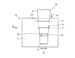
- FIG. 1 It is a partial top view which shows the 1st flexible printed wiring board which comprises the connection structure of the flexible printed wiring board which concerns on Embodiment 1 of this invention, and a 2nd flexible printed wiring board. It is a top view which shows the state by which the 1st flexible printed wiring board and the 2nd flexible printed wiring board were latched in the same embodiment. It is the side view seen from the arrow III direction of FIG. It is a top view which shows the state which connected the 1st wiring of the 1st flexible printed wiring board, and the 2nd wiring of the 2nd flexible printed wiring board with solder. It is the side view seen from the arrow V direction of FIG.
- FIG. 1 is a partial plan view showing a first flexible printed wiring board and a second flexible printed wiring board that constitute a flexible printed wiring board connection structure according to Embodiment 1 of the present invention.
- the first wiring 14 of the first flexible printed wiring board 10 and the second wiring of the second flexible printed wiring board 20. 22 is electrically connected.
- the first flexible printed wiring board 10 has a first wiring 14 on one main surface, extends at a predetermined interval from each other, and a part of the second flexible printed wiring board 20 is inserted therethrough. 1 opening 12 and 2nd opening 13 are included.
- Part of the second flexible printed wiring board 20 is inserted into the first flexible printed wiring board 10 in the direction indicated by the arrow 30 in the drawing.
- the width direction orthogonal to the insertion direction is the direction indicated by the arrow 31 in the drawing.
- the first wiring 14 is formed on one main surface of the substrate 11. In FIG. 1, only the soldering portion of the first wiring 14 is shown.
- a rectangular first opening 12 and a second opening 13 extending in the width direction are formed in the base material 11 substantially in parallel.
- the width in the width direction of the first opening 12 and the second opening 13 is L 0 .
- a space between the first opening 12 and the second opening 13 in the insertion direction is a folded portion 15 described later.
- the second flexible printed wiring board 20 has one main surface in a narrow width portion 26 having a width narrower than the width L 0 of the first opening 12 and the second opening 13 in the width direction and positioned at the distal end portion in the insertion direction.
- a positioning portion 24 having a second wiring 22 on the upper side and connected to the narrow width portion 26 and having a width L 2 wider than the width L 0 of the first opening 12 and the second opening 13 in the width direction is included.
- the narrow portion 26 of the second flexible printed wiring board 20 has a tapered shape whose width becomes wider as the distance from the tip 23 is the width L 1.
- the width L 2 of the positioning portion 24 is slightly wider than the width L 0 .
- the second wiring 22 is formed on one main surface of the base material 21. In FIG. 1, only the soldered portion of the second wiring 22 is shown. The soldering portion of the second wiring 22 is formed in the vicinity of the tip 23 of the second flexible printed wiring board 20.
- FIG. 2 is a plan view showing a state in which the first flexible printed wiring board and the second flexible printed wiring board are locked in the present embodiment.
- FIG. 3 is a side view seen from the direction of arrow III in FIG.
- the wiring board 20 is located on the other main surface side of the first flexible printed wiring board 10 between the first opening 12 and the second opening 13, and is opposite to the second opening 13 side of the first opening 12 and
- the second opening 13 is located on the one main surface side of the first flexible printed wiring board 10 on the side opposite to the first opening 12 side.
- the second flexible printed wiring board 20 is folded at the folded portion 15 located between the first opening 12 and the second opening 13.
- the width L 2 of the positioning part 24 of the second flexible printed wiring board 20 is slightly wider than the width L 0 of the first opening 12, when the narrow width part 26 passes through the first opening 12, the first opening 12 and the positioning part 24 is engaged.
- the soldered portion of the first wiring 14 of the first flexible printed wiring board 10 and the soldered portion of the second wiring 22 of the second flexible printed wiring board 20 are located close to each other.
- the second flexible printed wiring board 20 is positioned at a predetermined position with respect to the first flexible printed wiring board 10.
- FIG. 4 is a plan view showing a state where the first wiring of the first flexible printed wiring board and the second wiring of the second flexible printed wiring board are connected by soldering.
- FIG. 5 is a side view seen from the direction of arrow V in FIG.
- the solder 40 extends across the soldering portion of the first wiring 14 of the first flexible printed wiring board 10 and the soldering portion of the second wiring 22 of the second flexible printed wiring board 20. Applied. The first flexible printed wiring board 10 and the second flexible printed wiring board 20 are electrically connected by the solder 40.
- first flexible printed wiring board 10 and the second flexible printed wiring board 20 are engaged by the engagement of the first opening 12 of the first flexible printed wiring board 10 and the positioning portion 24 of the second flexible printed wiring board 20.
- the first wiring 14 and the second wiring 22 are connected in a locked state.
- the width direction indicated by the arrow 31 with respect to the base material 21 of the second flexible printed wiring board 20 is as follows.
- the second flexible printed circuit is formed by the folded portion 15 of the first flexible printed wiring board 10. Since the wiring board 20 is folded, it can suppress that force acts on the connection part by the solder 40.
- first opening 12 and the second opening 13 are parallel to each other and have the same width.
- present invention is not limited to this, and the extending direction of the first opening 12 and the second opening 13 The extending directions may intersect and have different widths.
- connection structure of the flexible printed wiring board according to the second embodiment of the present invention will be described.
- the connection structure of the flexible printed wiring board according to the present embodiment is different from the connection structure of the flexible printed wiring board according to the first embodiment only in the positions of the first opening and the second opening of the first flexible printed wiring board. The description of the configuration will not be repeated.
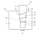
- FIG. 6 is a partial plan view showing a first flexible printed wiring board and a second flexible printed wiring board constituting a flexible printed wiring board connection structure according to Embodiment 2 of the present invention.
- the first wiring 14 of the first flexible printed wiring board 50 and the second wiring of the second flexible printed wiring board 20. 22 is electrically connected.
- the first flexible printed wiring board 50 has a first wiring 14 on one main surface, extends at a predetermined interval from each other, and a part of the second flexible printed wiring board 20 is inserted therethrough.
- a first opening 52 and a second opening 53 are included.
- the first wiring 14 is formed on one main surface of the substrate 11. In FIG. 6, only the soldering portion of the first wiring 14 is shown.
- first openings 52 and second openings 53 extending in a direction intersecting with the insertion direction at an angle ⁇ are formed substantially in parallel.
- the width in the width direction of the first opening 52 and the second opening 53 is L 0 .
- a space between the first opening 52 and the second opening 53 in the insertion direction is a folded portion 55.
- the angle ⁇ is an acute angle. That is, the insertion direction and the extending direction of the first opening 52 intersect at an acute angle.
- FIG. 7 is a plan view showing a state in which the tip of the second flexible printed wiring board is inserted into the first opening of the first flexible printed wiring board in the present embodiment.
- the tip 23 of the second flexible printed wiring board 20 is inserted into the first opening 52 of the first flexible printed wiring board 50.
- the tip corner 25 first passes through the first opening 52.
- the 1st flexible printed wiring board 50 is easy.
- the narrow portion 26 of the second flexible printed wiring board 20 can be inserted into the first opening 52.
- the tip angle of the second flexible printed wiring board 20 is inserted into the second opening 53 of the first flexible printed wiring board 50.
- the part 25 first passes through the second opening 53.
- FIG. 8 is a plan view showing a state in which the first flexible printed wiring board and the second flexible printed wiring board are locked in the present embodiment.
- the second flexible printed wiring board. 20 is located on the other main surface side of the first flexible printed wiring board 50 between the first opening 52 and the second opening 53, and the second opening 53 side opposite to the second opening 53 side and the second opening.
- the opening 53 is located on one side of the first flexible printed wiring board 10 on the side opposite to the first opening 52 side.
- the second flexible printed wiring board 20 is folded back at the folded portion 55 located between the first opening 52 and the second opening 53.
- the width L 2 of the positioning portion 24 of the second flexible printed wiring board 20 is slightly wider than the width L 0 of the first opening 52 in the width direction, when the narrow width portion 26 passes through the first opening 52, the first opening 52 and the positioning part 24 engage.
- the soldering portion of the first wiring 14 of the first flexible printed wiring board 50 and the soldering portion of the second wiring 22 of the second flexible printed wiring board 20 are located close to each other. In this manner, the second flexible printed wiring board 20 is positioned at a predetermined position with respect to the first flexible printed wiring board 50.
- Solder is applied across the soldered portion of the first wiring 14 of the first flexible printed wiring board 50 and the soldered portion of the second wiring 22 of the second flexible printed wiring board 20.
- the first flexible printed wiring board 50 and the second flexible printed wiring board 20 are electrically connected by solder.
- first flexible printed wiring board 50 and the second flexible printed wiring board 20 are engaged by the engagement of the first opening 52 of the first flexible printed wiring board 50 and the positioning portion 24 of the second flexible printed wiring board 20.
- the first wiring 14 and the second wiring 22 are connected in a locked state.
- the width direction indicated by the arrow 31 with respect to the base material 21 of the second flexible printed wiring board 20 is as follows.
- the first opening 52 of the first flexible printed wiring board 50 and the positioning portion 24 of the second flexible printed wiring board 20 are engaged with each other, so that the force acts on the connecting portion by solder. This can be suppressed.
- the second flexible printed wiring board is folded at the folded portion 55 of the first flexible printed wiring board 50. Since 20 is folded, it can suppress that force acts on the connection part by solder.
- first opening 52 and the second opening 53 are parallel to each other and have the same width.
- present invention is not limited to this, and the extending direction of the first opening 52 and the second opening 53 The extending directions may intersect and have different widths.
- connection structure of the flexible printed wiring board according to Embodiment 3 of the present invention will be described.
- connection structure of the flexible printed wiring board which concerns on this embodiment is only the width
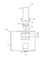
- FIG. 9 is a partial plan view showing a first flexible printed wiring board and a second flexible printed wiring board constituting a flexible printed wiring board connection structure according to Embodiment 3 of the present invention.
- the first wiring 14 of the first flexible printed wiring board 60 and the second wiring of the second flexible printed wiring board 70. 72 is electrically connected.
- the first flexible printed wiring board 60 has the first wiring 14 on one main surface, extends at a predetermined interval from each other, and a part of the second flexible printed wiring board 70 is inserted therethrough. 1 opening 62 and 2nd opening 13 are included.
- the first wiring 14 is formed on one main surface of the substrate 11. In FIG. 9, only the soldering portion of the first wiring 14 is shown.
- a rectangular first opening 62 and a second opening 13 extending in the width direction are formed in the base material 11 substantially in parallel.
- the width of the first opening 62 in the width direction is L 3 .
- the width of the second opening 13 in the width direction is L 0 .
- L 3 > L 0 and the first opening 62 has a width wider than the second opening 13 in the width direction.
- a portion 65 between the first opening 62 and the second opening 13 in the insertion direction is a folded portion 65.
- the second flexible printed wiring board 70 has a constant width narrower than the width L 0 of the second opening 13 in the width direction and has a first width on one main surface in a narrow width portion 76 located at the tip in the insertion direction.
- a positioning portion 74 having two wirings 72 and connected to the narrow width portion 76 and having a width L 4 wider than the width L 0 of the second opening 13 in the width direction is included.
- Positioning portion 74 has the width L 4 than the width L 0 of the second opening 13 in the narrower and the width direction than the width L 3 of the first opening 62 in the width direction.
- the positioning part 74 is formed at the end of the narrow part 76 so as to protrude in the width direction.
- the second wiring 72 is formed on one main surface of the base material 71. In FIG. 9, only the soldered portion of the second wiring 72 is shown. The soldering portion of the second wiring 72 is formed in the vicinity of the tip 73 of the second flexible printed wiring board 70.
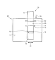
- FIG. 10 is a plan view showing a state in which the first flexible printed wiring board and the second flexible printed wiring board are locked in the present embodiment.
- the second flexible printed wiring board in a state where the narrow portion 76 of the second flexible printed wiring board 70 is inserted into the first opening 62 and the second opening 13 of the first flexible printed wiring board 60.
- 70 is located on the other main surface side of the first flexible printed wiring board 60 between the first opening 62 and the second opening 13, and is opposite to the second opening 13 side and the second opening of the first opening 62.
- the opening 13 is located on the one main surface side of the first flexible printed wiring board 60 on the side opposite to the first opening 62 side.
- the second flexible printed wiring board 70 is folded back at the folded portion 65 located between the first opening 62 and the second opening 13.
- the width L 4 of the positioning portion 74 of the second flexible printed wiring board 70 is wider than the width L 0 of the second opening 13, when the narrow width portion 76 passes through the second opening 13, the second opening 13, the positioning portion 74, Engage.
- the soldered portion of the first wiring 14 of the first flexible printed wiring board 60 and the soldered portion of the second wiring 72 of the second flexible printed wiring board 70 are located close to each other.
- the second flexible printed wiring board 70 is positioned at a predetermined position with respect to the first flexible printed wiring board 60.
- Solder is applied across the soldered portion of the first wiring 14 of the first flexible printed wiring board 60 and the soldered portion of the second wiring 72 of the second flexible printed wiring board 70.
- the first flexible printed wiring board 60 and the second flexible printed wiring board 70 are electrically connected by solder.
- first flexible printed wiring board 60 and the second flexible printed wiring board 70 are engaged by the engagement of the second opening 13 of the first flexible printed wiring board 60 and the positioning portion 74 of the second flexible printed wiring board 70.
- the first wiring 14 and the second wiring 72 are connected.
- the width direction indicated by the arrow 31 with respect to the base material 71 of the second flexible printed wiring board 70 is as follows.
- the second opening 13 of the first flexible printed wiring board 60 and the positioning portion 74 of the second flexible printed wiring board 70 are engaged with each other, so that the force acts on the connecting portion by solder. This can be suppressed.
- the second flexible printed wiring board 70 is folded by the folded portion 65 of the first flexible printed wiring board 60. Since 70 is folded back, it can suppress that force acts on the connection part by solder.
- first opening 62 and the second opening 13 are parallel to each other.
- present invention is not limited to this, and the extending direction of the first opening 62 and the extending direction of the second opening 13 intersect. You may do it.
Landscapes
- Engineering & Computer Science (AREA)
- Manufacturing & Machinery (AREA)
- Microelectronics & Electronic Packaging (AREA)
- Combinations Of Printed Boards (AREA)
Abstract
第1フレキシブルプリント配線板(10)は、第1配線(14)を有して、互いに所定の間隔を置いて延在して第2フレキシブルプリント配線板(20)の一部が挿通される第1開口(12)および第2開口(13)を含む。第2フレキシブルプリント配線板(20)は、第1フレキシブルプリント配線板(10)への挿通方向(30)に直交する幅方向(31)において第1開口(12)および第2開口(13)の幅より狭い幅を持って挿通方向(30)の先端部に位置する狭幅部(26)において第2配線(22)を有して、狭幅部(26)に繋がって上記幅方向(31)において第1開口(12)および第2開口(13)のいずれかの幅より広い幅を持つ位置決め部(24)を含む。第1開口(12)または第2開口(13)と位置決め部(24)とが係合することにより第1フレキシブルプリント配線板(10)と第2フレキシブルプリント配線板(20)とが係止された状態で、第1配線(14)と第2配線(22)とが接続されている。
Description
本発明は、フレキシブルプリント配線板の接続構造に関し、特に、フレキシブルプリント配線板同士の接続構造に関する。
フレキシブルプリント配線板の接続構造を開示した先行文献として、実開平4-116176号公報(特許文献1)がある。特許文献1に記載されたフレキシブルプリント配線板の接続構造においては、硬質基板とフレキシブルプリント配線板との電気的な接続部と、硬質基板に形成されたフレキシブルプリント配線板の幅と等しい長さの切欠きとフレキシブルプリント配線板に形成された切欠きとが組み合わされる硬質基板とフレキシブルプリント配線板との係合部とが構成される。
硬質基板に形成された切欠きとフレキシブルプリント配線板に形成された切欠きとを係合させて硬質基板とフレキシブルプリント配線板とを係止する場合、フレキシブルプリント配線板に力が負荷された際に切欠き同士の係合が外れやすいため、硬質基板とフレキシブルプリント配線板との接続部に力が作用することを安定して防止することができない。
本発明は上記の問題点に鑑みてなされたものであって、フレキシブルプリント配線板を所定の位置で位置決めしつつ接続部に力が作用することを抑制することができる、フレキシブルプリント配線板の接続構造を提供することを目的とする。
本発明に基づくフレキシブルプリント配線板の接続構造は、第1フレキシブルプリント配線板の第1配線と第2フレキシブルプリント配線板の第2配線とを電気的に接続するフレキシブルプリント配線板の接続構造である。第1フレキシブルプリント配線板は、一方の主面上に第1配線を有して、互いに所定の間隔を置いて延在して第2フレキシブルプリント配線板の一部が挿通される第1開口および第2開口を含む。第2フレキシブルプリント配線板は、第1フレキシブルプリント配線板への挿通方向に直交する幅方向において第1開口および第2開口の幅より狭い幅を持って挿通方向の先端部に位置する狭幅部において一方の主面上に第2配線を有して、狭幅部に繋がって上記幅方向において第1開口および第2開口のいずれかの幅より広い幅を持つ位置決め部を含む。第1開口および第2開口に狭幅部が挿通された状態において、第2フレキシブルプリント配線板は、第1開口と第2開口との間で第1フレキシブルプリント配線板の他方の主面側に位置し、第1開口の第2開口側とは反対側および第2開口の第1開口側とは反対側で第1フレキシブルプリント配線板の一方の主面側に位置する。第1開口または第2開口と位置決め部とが係合することにより第1フレキシブルプリント配線板と第2フレキシブルプリント配線板とが係止された状態で、第1配線と第2配線とが接続されている。
本発明の一形態においては、上記挿通方向と第1開口の延在方向とが鋭角に交差している。
本発明の一形態においては、第2フレキシブルプリント配線板の狭幅部は、先端から離れるにしたがって幅が広くなるテーパ形状を有している。
本発明の一形態においては、第1開口が上記幅方向において第2開口より広い幅を持っている。狭幅部は上記幅方向における第2開口の幅より狭い一定の幅を持っている。位置決め部は、上記幅方向における第1開口の幅より狭くかつ上記幅方向における第2開口の幅より広い幅を持っている。
本発明によれば、フレキシブルプリント配線板を所定の位置で位置決めしつつ接続部に力が作用することを抑制することができる。
以下、本発明の実施形態1に係るフレキシブルプリント配線板の接続構造について説明する。以下の実施形態の説明においては、図中の同一または相当部分には同一符号を付して、その説明は繰り返さない。なお、実施形態の説明において、説明の便宜上、上、下、左、右の表現を用いるが、これらの表現は示した図に基づくものであって発明の構成を限定するものではない。
(実施形態1)
図1は、本発明の実施形態1に係るフレキシブルプリント配線板の接続構造を構成する第1フレキシブルプリント配線板および第2フレキシブルプリント配線板を示す一部平面図である。
図1は、本発明の実施形態1に係るフレキシブルプリント配線板の接続構造を構成する第1フレキシブルプリント配線板および第2フレキシブルプリント配線板を示す一部平面図である。
図1に示すように、本発明の実施形態1に係るフレキシブルプリント配線板の接続構造においては、第1フレキシブルプリント配線板10の第1配線14と、第2フレキシブルプリント配線板20の第2配線22とが電気的に接続される。
第1フレキシブルプリント配線板10は、一方の主面上に第1配線14を有して、互いに所定の間隔を置いて延在して第2フレキシブルプリント配線板20の一部が挿通される第1開口12および第2開口13を含む。
第2フレキシブルプリント配線板20の一部は、第1フレキシブルプリント配線板10に対して、図中の矢印30で示す向きに挿通される。この挿通方向に直交する幅方向は、図中の矢印31で示す向きである。
第1フレキシブルプリント配線板10においては、基材11の一方の主面上に第1配線14が形成されている。図1においては、第1配線14の半田付け部のみ図示している。
基材11には、上記幅方向に延在する矩形状の第1開口12および第2開口13が略平行に形成されている。第1開口12および第2開口13の上記幅方向の幅はL0である。上記挿通方向における第1開口12と第2開口13との間が、後述する折返し部15となる。
第2フレキシブルプリント配線板20は、上記幅方向において第1開口12および第2開口13の幅L0より狭い幅を持って上記挿通方向の先端部に位置する狭幅部26において一方の主面上に第2配線22を有して、狭幅部26に繋がって上記幅方向において第1開口12および第2開口13の幅L0より広い幅L2を持つ位置決め部24を含む。
本実施形態においては、第2フレキシブルプリント配線板20の狭幅部26は、幅L1である先端23から離れるにしたがって幅が広くなるテーパ形状を有している。位置決め部24の幅L2は、幅L0より僅かに広い。
第2フレキシブルプリント配線板20においては、基材21の一方の主面上に第2配線22が形成されている。図1においては、第2配線22の半田付け部のみ図示している。第2配線22の半田付け部は、第2フレキシブルプリント配線板20の先端23の近傍に形成されている。
図2は、本実施形態において第1フレキシブルプリント配線板と第2フレキシブルプリント配線板とが係止された状態を示す平面図である。図3は、図2の矢印III方向から見た側面図である。
図2,3に示すように、第1フレキシブルプリント配線板10の第1開口12および第2開口13に第2フレキシブルプリント配線板20の狭幅部26が挿通された状態において、第2フレキシブルプリント配線板20は、第1開口12と第2開口13との間で第1フレキシブルプリント配線板10の他方の主面側に位置し、第1開口12の第2開口13側とは反対側および第2開口13の第1開口12側とは反対側で第1フレキシブルプリント配線板10の一方の主面側に位置している。
すなわち、第2フレキシブルプリント配線板20は、第1開口12と第2開口13との間に位置する折返し部15で折り返されている。
第2フレキシブルプリント配線板20の位置決め部24の幅L2は第1開口12の幅L0より僅かに広いため、狭幅部26が第1開口12を通過すると、第1開口12と位置決め部24とが係合する。
その状態で、第1フレキシブルプリント配線板10の第1配線14の半田付け部と第2フレキシブルプリント配線板20の第2配線22の半田付け部とが近接して位置している。このように、第2フレキシブルプリント配線板20は、第1フレキシブルプリント配線板10に対して所定の位置で位置決めされる。
図4は、第1フレキシブルプリント配線板の第1配線と第2フレキシブルプリント配線板の第2配線とを半田で接続した状態を示す平面図である。図5は、図4の矢印V方向から見た側面図である。
図4,5に示すように、第1フレキシブルプリント配線板10の第1配線14の半田付け部と第2フレキシブルプリント配線板20の第2配線22の半田付け部とに跨るように半田40が塗布される。半田40により第1フレキシブルプリント配線板10と第2フレキシブルプリント配線板20とが電気的に接続される。
すなわち、第1フレキシブルプリント配線板10の第1開口12と第2フレキシブルプリント配線板20の位置決め部24とが係合することにより第1フレキシブルプリント配線板10と第2フレキシブルプリント配線板20とが係止された状態で、第1配線14と第2配線22とが接続されている。
上記のように第1フレキシブルプリント配線板10と第2フレキシブルプリント配線板20とを電気的に接続することにより、第2フレキシブルプリント配線板20の基材21に対して矢印31で示す幅方向の力が負荷された場合に、第1フレキシブルプリント配線板10の第1開口12と第2フレキシブルプリント配線板20の位置決め部24とが係合しているため、半田40による接続部に力が作用することを抑制することができる。
また、第2フレキシブルプリント配線板20の基材21に対して図5中の矢印32で示す方向の力が負荷された場合に、第1フレキシブルプリント配線板10の折返し部15で第2フレキシブルプリント配線板20が折り返されているため、半田40による接続部に力が作用することを抑制することができる。
すなわち、第2フレキシブルプリント配線板20を第1フレキシブルプリント配線板10に対して所定の位置で位置決めしつつ半田40による接続部に力が作用することを抑制することができる。その結果、安定して第1フレキシブルプリント配線板10と第2フレキシブルプリント配線板20とを接続しつつ接続部の耐久性を向上することができる。
なお、本実施形態においては、第1開口12と第2開口13とは互いに平行で同じ幅を有していたが、これに限られず、第1開口12の延在方向と第2開口13の延在方向とが交差して互いに異なる幅を有していてもよい。
以下、本発明の実施形態2に係るフレキシブルプリント配線板の接続構造について説明する。なお、本実施形態に係るフレキシブルプリント配線板の接続構造は、第1フレキシブルプリント配線板の第1開口および第2開口の位置のみ実施形態1に係るフレキシブルプリント配線板の接続構造と異なるため、他の構成については説明を繰り返さない。
(実施形態2)
図6は、本発明の実施形態2に係るフレキシブルプリント配線板の接続構造を構成する第1フレキシブルプリント配線板および第2フレキシブルプリント配線板を示す一部平面図である。
図6は、本発明の実施形態2に係るフレキシブルプリント配線板の接続構造を構成する第1フレキシブルプリント配線板および第2フレキシブルプリント配線板を示す一部平面図である。
図6に示すように、本発明の実施形態2に係るフレキシブルプリント配線板の接続構造においては、第1フレキシブルプリント配線板50の第1配線14と、第2フレキシブルプリント配線板20の第2配線22とが電気的に接続される。
第1フレキシブルプリント配線板50は、一方の主面上に第1配線14を有して、互いに所定の間隔を置いて延在して第2フレキシブルプリント配線板20の一部が挿通される第1開口52および第2開口53を含む。
第1フレキシブルプリント配線板50においては、基材11の一方の主面上に第1配線14が形成されている。図6においては、第1配線14の半田付け部のみ図示している。
基材11には、上記挿通方向に対して角度θで交差する方向に延在する矩形状の第1開口52および第2開口53が略平行に形成されている。第1開口52および第2開口53の上記幅方向の幅はL0である。上記挿通方向における第1開口52と第2開口53との間が、折返し部55となる。
本実施形態においては、角度θは鋭角である。すなわち、上記挿通方向と第1開口52の延在方向とが鋭角に交差している。
図7は、本実施形態において第1フレキシブルプリント配線板の第1開口に第2フレキシブルプリント配線板の先端を挿入させた状態を示す平面図である。
図7に示すように、第1開口52が上記挿通方向に対して傾斜しているため、第1フレキシブルプリント配線板50の第1開口52に第2フレキシブルプリント配線板20の先端23を挿入する際、先端角部25が最初に第1開口52を通過する。
このようにすることにより、第2フレキシブルプリント配線板20の先端23全体を同時に第1フレキシブルプリント配線板50の第1開口52に挿入する場合に比べて、容易に第1フレキシブルプリント配線板50の第1開口52に第2フレキシブルプリント配線板20の狭幅部26を挿通させることができる。
同様に、第2開口53が上記挿通方向に対して傾斜しているため、第1フレキシブルプリント配線板50の第2開口53に第2フレキシブルプリント配線板20の先端23を挿入する際、先端角部25が最初に第2開口53を通過する。
このようにすることにより、第2フレキシブルプリント配線板20の先端23全体を同時に第1フレキシブルプリント配線板50の第2開口53に挿入する場合に比べて、容易に第1フレキシブルプリント配線板50の第2開口53に第2フレキシブルプリント配線板20の狭幅部26を挿通させて折り返すことができる。
図8は、本実施形態において第1フレキシブルプリント配線板と第2フレキシブルプリント配線板とが係止された状態を示す平面図である。
図8に示すように、第1フレキシブルプリント配線板50の第1開口52および第2開口53に第2フレキシブルプリント配線板20の狭幅部26が挿通された状態において、第2フレキシブルプリント配線板20は、第1開口52と第2開口53との間で第1フレキシブルプリント配線板50の他方の主面側に位置し、第1開口52の第2開口53側とは反対側および第2開口53の第1開口52側とは反対側で第1フレキシブルプリント配線板10の一方の主面側に位置している。
すなわち、第2フレキシブルプリント配線板20は、第1開口52と第2開口53との間に位置する折返し部55で折り返されている。
第2フレキシブルプリント配線板20の位置決め部24の幅L2は第1開口52の上記幅方向の幅L0より僅かに広いため、狭幅部26が第1開口52を通過すると、第1開口52と位置決め部24とが係合する。
その状態で、第1フレキシブルプリント配線板50の第1配線14の半田付け部と第2フレキシブルプリント配線板20の第2配線22の半田付け部とが近接して位置している。このように、第2フレキシブルプリント配線板20は、第1フレキシブルプリント配線板50に対して所定の位置で位置決めされる。
第1フレキシブルプリント配線板50の第1配線14の半田付け部と第2フレキシブルプリント配線板20の第2配線22の半田付け部とに跨るように半田が塗布される。半田により第1フレキシブルプリント配線板50と第2フレキシブルプリント配線板20とが電気的に接続される。
すなわち、第1フレキシブルプリント配線板50の第1開口52と第2フレキシブルプリント配線板20の位置決め部24とが係合することにより第1フレキシブルプリント配線板50と第2フレキシブルプリント配線板20とが係止された状態で、第1配線14と第2配線22とが接続されている。
上記のように第1フレキシブルプリント配線板50と第2フレキシブルプリント配線板20とを電気的に接続することにより、第2フレキシブルプリント配線板20の基材21に対して矢印31で示す幅方向の力が負荷された場合に、第1フレキシブルプリント配線板50の第1開口52と第2フレキシブルプリント配線板20の位置決め部24とが係合しているため、半田による接続部に力が作用することを抑制することができる。
また、第2フレキシブルプリント配線板20の基材21に対して上記挿通方向とは反対方向の力が負荷された場合に、第1フレキシブルプリント配線板50の折返し部55で第2フレキシブルプリント配線板20が折り返されているため、半田による接続部に力が作用することを抑制することができる。
すなわち、第2フレキシブルプリント配線板20を第1フレキシブルプリント配線板50に対して所定の位置で位置決めしつつ半田による接続部に力が作用することを抑制することができる。その結果、安定して第1フレキシブルプリント配線板50と第2フレキシブルプリント配線板20とを接続しつつ接続部の耐久性を向上することができる。
なお、本実施形態においては、第1開口52と第2開口53とは互いに平行で同じ幅を有していたが、これに限られず、第1開口52の延在方向と第2開口53の延在方向とが交差して互いに異なる幅を有していてもよい。
以下、本発明の実施形態3に係るフレキシブルプリント配線板の接続構造について説明する。なお、本実施形態に係るフレキシブルプリント配線板の接続構造は、第1フレキシブルプリント配線板の第1開口の幅、および、第2フレキシブルプリント配線板の形状のみ実施形態1に係るフレキシブルプリント配線板の接続構造と異なるため、他の構成については説明を繰り返さない。
(実施形態3)
図9は、本発明の実施形態3に係るフレキシブルプリント配線板の接続構造を構成する第1フレキシブルプリント配線板および第2フレキシブルプリント配線板を示す一部平面図である。
図9は、本発明の実施形態3に係るフレキシブルプリント配線板の接続構造を構成する第1フレキシブルプリント配線板および第2フレキシブルプリント配線板を示す一部平面図である。
図9に示すように、本発明の実施形態3に係るフレキシブルプリント配線板の接続構造においては、第1フレキシブルプリント配線板60の第1配線14と、第2フレキシブルプリント配線板70の第2配線72とが電気的に接続される。
第1フレキシブルプリント配線板60は、一方の主面上に第1配線14を有して、互いに所定の間隔を置いて延在して第2フレキシブルプリント配線板70の一部が挿通される第1開口62および第2開口13を含む。
第1フレキシブルプリント配線板60においては、基材11の一方の主面上に第1配線14が形成されている。図9においては、第1配線14の半田付け部のみ図示している。
基材11には、上記幅方向に延在する矩形状の第1開口62および第2開口13が略平行に形成されている。第1開口62の上記幅方向の幅はL3である。第2開口13の上記幅方向の幅はL0である。L3>L0であり、第1開口62は上記幅方向において第2開口13より広い幅を持っている。上記挿通方向における第1開口62と第2開口13との間が、折返し部65となる。
第2フレキシブルプリント配線板70は、上記幅方向において第2開口13の幅L0より狭い一定の幅を持って上記挿通方向の先端部に位置する狭幅部76において一方の主面上に第2配線72を有して、狭幅部76に繋がって上記幅方向において第2開口13の幅L0より広い幅L4を持つ位置決め部74を含む。
位置決め部74は、上記幅方向における第1開口62の幅L3より狭くかつ幅方向における第2開口13の幅L0より広い幅L4を持っている。位置決め部74は、狭幅部76の端部において、上記幅方向に突き出すように形成されている。
第2フレキシブルプリント配線板70においては、基材71の一方の主面上に第2配線72が形成されている。図9においては、第2配線72の半田付け部のみ図示している。第2配線72の半田付け部は、第2フレキシブルプリント配線板70の先端73の近傍に形成されている。
図10は、本実施形態において第1フレキシブルプリント配線板と第2フレキシブルプリント配線板とが係止された状態を示す平面図である。
図10に示すように、第1フレキシブルプリント配線板60の第1開口62および第2開口13に第2フレキシブルプリント配線板70の狭幅部76が挿通された状態において、第2フレキシブルプリント配線板70は、第1開口62と第2開口13との間で第1フレキシブルプリント配線板60の他方の主面側に位置し、第1開口62の第2開口13側とは反対側および第2開口13の第1開口62側とは反対側で第1フレキシブルプリント配線板60の一方の主面側に位置している。
すなわち、第2フレキシブルプリント配線板70は、第1開口62と第2開口13との間に位置する折返し部65で折り返されている。
第2フレキシブルプリント配線板70の位置決め部74の幅L4は第2開口13の幅L0より広いため、狭幅部76が第2開口13を通過すると、第2開口13と位置決め部74とが係合する。
その状態で、第1フレキシブルプリント配線板60の第1配線14の半田付け部と第2フレキシブルプリント配線板70の第2配線72の半田付け部とが近接して位置している。このように、第2フレキシブルプリント配線板70は、第1フレキシブルプリント配線板60に対して所定の位置で位置決めされる。
第1フレキシブルプリント配線板60の第1配線14の半田付け部と第2フレキシブルプリント配線板70の第2配線72の半田付け部とに跨るように半田が塗布される。半田により第1フレキシブルプリント配線板60と第2フレキシブルプリント配線板70とが電気的に接続される。
すなわち、第1フレキシブルプリント配線板60の第2開口13と第2フレキシブルプリント配線板70の位置決め部74とが係合することにより第1フレキシブルプリント配線板60と第2フレキシブルプリント配線板70とが係止された状態で、第1配線14と第2配線72とが接続される。
上記のように第1フレキシブルプリント配線板60と第2フレキシブルプリント配線板70とを電気的に接続することにより、第2フレキシブルプリント配線板70の基材71に対して矢印31で示す幅方向の力が負荷された場合に、第1フレキシブルプリント配線板60の第2開口13と第2フレキシブルプリント配線板70の位置決め部74とが係合しているため、半田による接続部に力が作用することを抑制することができる。
また、第2フレキシブルプリント配線板70の基材71に対して上記挿通方向とは反対方向の力が負荷された場合に、第1フレキシブルプリント配線板60の折返し部65で第2フレキシブルプリント配線板70が折り返されているため、半田による接続部に力が作用することを抑制することができる。
すなわち、第2フレキシブルプリント配線板70を第1フレキシブルプリント配線板60に対して所定の位置で位置決めしつつ半田による接続部に力が作用することを抑制することができる。その結果、安定して第1フレキシブルプリント配線板60と第2フレキシブルプリント配線板70とを接続しつつ接続部の耐久性を向上することができる。
なお、本実施形態においては、第1開口62と第2開口13とは互いに平行であるが、これに限られず、第1開口62の延在方向と第2開口13の延在方向とが交差していてもよい。
今回開示された実施形態はすべての点で例示であって制限的なものではないと考えられるべきである。本発明の範囲は上記した説明ではなくて請求の範囲によって示され、請求の範囲と均等の意味および範囲内でのすべての変更が含まれることが意図される。
10,50,60 第1フレキシブルプリント配線板、11,21,71 基材、12,52,62 第1開口、13,53 第2開口、14 第1配線、15,55,65 折返し部、20,70 第2フレキシブルプリント配線板、22,72 第2配線、23,73 先端、24,74 位置決め部、25 先端角部、26,76 狭幅部、40 半田。
Claims (4)
- 第1フレキシブルプリント配線板(10,50,60)の第1配線(14)と第2フレキシブルプリント配線板(20,70)の第2配線(22,72)とを電気的に接続するフレキシブルプリント配線板の接続構造であって、
前記第1フレキシブルプリント配線板(10,50,60)は、一方の主面上に前記第1配線(14)を有して、互いに所定の間隔を置いて延在して前記第2フレキシブルプリント配線板(20,70)の一部が挿通される第1開口(12,52,62)および第2開口(13,53)を含み、
前記第2フレキシブルプリント配線板(20,70)は、前記第1フレキシブルプリント配線板(10,50,60)への挿通方向に直交する幅方向において前記第1開口(12,52,62)および前記第2開口(13,53)の幅より狭い幅を持って前記挿通方向の先端部に位置する狭幅部(26,76)において一方の主面上に前記第2配線(22,72)を有して、前記狭幅部(26,76)に繋がって前記幅方向において前記第1開口(12,52,62)および前記第2開口(13,53)のいずれかの幅より広い幅を持つ位置決め部(24,74)を含み、
前記第1開口(12,52,62)および前記第2開口(13,53)に前記狭幅部(26,76)が挿通された状態において、前記第2フレキシブルプリント配線板(20,70)は、前記第1開口(12,52,62)と前記第2開口(13,53)との間で前記第1フレキシブルプリント配線板(10,50,60)の他方の主面側に位置し、前記第1開口(12,52,62)の前記第2開口(13,53)側とは反対側および前記第2開口(13,53)の前記第1開口(12,52,62)側とは反対側で前記第1フレキシブルプリント配線板(10,50,60)の一方の主面側に位置し、
前記第1開口(12,52,62)または前記第2開口(13,53)と前記位置決め部(24,74)とが係合することにより前記第1フレキシブルプリント配線板(10,50,60)と前記第2フレキシブルプリント配線板(20,70)とが係止された状態で、前記第1配線(14)と前記第2配線(22,72)とが接続されている、フレキシブルプリント配線板の接続構造。 - 前記挿通方向と前記第1開口(52)の延在方向とが鋭角に交差している、請求項1に記載のフレキシブルプリント配線板の接続構造。
- 前記第2フレキシブルプリント配線板(20)の前記狭幅部(26)は、前記先端から離れるにしたがって幅が広くなるテーパ形状を有している、請求項1または2に記載のフレキシブルプリント配線板の接続構造。
- 前記第1開口(62)が前記幅方向において前記第2開口(13)より広い幅を持ち、
前記狭幅部(76)は前記幅方向における前記第2開口(13)の幅より狭い一定の幅を持ち、
前記位置決め部(74)は、前記幅方向における前記第1開口(62)の幅より狭くかつ前記幅方向における前記第2開口(13)の幅より広い幅を持っている、請求項1または2に記載のフレキシブルプリント配線板の接続構造。
Priority Applications (1)
| Application Number | Priority Date | Filing Date | Title |
|---|---|---|---|
| US14/117,849 US20140065853A1 (en) | 2011-05-23 | 2012-05-16 | Connecting structure for flexible printed wiring boards |
Applications Claiming Priority (2)
| Application Number | Priority Date | Filing Date | Title |
|---|---|---|---|
| JP2011114434 | 2011-05-23 | ||
| JP2011-114434 | 2011-05-23 |
Publications (1)
| Publication Number | Publication Date |
|---|---|
| WO2012161046A1 true WO2012161046A1 (ja) | 2012-11-29 |
Family
ID=47217126
Family Applications (1)
| Application Number | Title | Priority Date | Filing Date |
|---|---|---|---|
| PCT/JP2012/062502 Ceased WO2012161046A1 (ja) | 2011-05-23 | 2012-05-16 | フレキシブルプリント配線板の接続構造 |
Country Status (2)
| Country | Link |
|---|---|
| US (1) | US20140065853A1 (ja) |
| WO (1) | WO2012161046A1 (ja) |
Families Citing this family (4)
| Publication number | Priority date | Publication date | Assignee | Title |
|---|---|---|---|---|
| CN105376937B (zh) * | 2015-11-10 | 2018-11-20 | 武汉华星光电技术有限公司 | 一种fpc结构 |
| FI20175786A1 (en) | 2017-09-01 | 2019-03-02 | Teknologian Tutkimuskeskus Vtt Oy | Electric membrane |
| EP4546761A4 (en) * | 2022-08-18 | 2025-09-10 | Samsung Electronics Co Ltd | ELECTRONIC DEVICE COMPRISING A FIXING ELEMENT |
| JP2025069775A (ja) * | 2023-10-18 | 2025-05-01 | アルプスアルパイン株式会社 | フレキシブル配線基板の規制装置および前記規制装置を用いた表示装置 |
Citations (5)
| Publication number | Priority date | Publication date | Assignee | Title |
|---|---|---|---|---|
| JPS6116708Y2 (ja) * | 1980-03-19 | 1986-05-22 | ||
| JPH08102575A (ja) * | 1994-09-30 | 1996-04-16 | Toshiba Corp | 基板接続機構 |
| JP2002270979A (ja) * | 2001-03-06 | 2002-09-20 | Aiwa Co Ltd | 導電部材の取付構造および取付方法 |
| JP2002359447A (ja) * | 2001-05-30 | 2002-12-13 | Sumitomo Wiring Syst Ltd | フラットケーブルとプリント基板の接続構造 |
| WO2009037796A1 (ja) * | 2007-09-21 | 2009-03-26 | Mitsubishi Electric Corporation | フレキシブル配線基板の固定構造 |
Family Cites Families (2)
| Publication number | Priority date | Publication date | Assignee | Title |
|---|---|---|---|---|
| JP2002141631A (ja) * | 2000-10-31 | 2002-05-17 | Yazaki Corp | フレキシブル回路体の接続構造 |
| US6538207B1 (en) * | 2002-01-18 | 2003-03-25 | Agilent Technologies, Inc. | Strain relief structures for lead connections |
-
2012
- 2012-05-16 WO PCT/JP2012/062502 patent/WO2012161046A1/ja not_active Ceased
- 2012-05-16 US US14/117,849 patent/US20140065853A1/en not_active Abandoned
Patent Citations (5)
| Publication number | Priority date | Publication date | Assignee | Title |
|---|---|---|---|---|
| JPS6116708Y2 (ja) * | 1980-03-19 | 1986-05-22 | ||
| JPH08102575A (ja) * | 1994-09-30 | 1996-04-16 | Toshiba Corp | 基板接続機構 |
| JP2002270979A (ja) * | 2001-03-06 | 2002-09-20 | Aiwa Co Ltd | 導電部材の取付構造および取付方法 |
| JP2002359447A (ja) * | 2001-05-30 | 2002-12-13 | Sumitomo Wiring Syst Ltd | フラットケーブルとプリント基板の接続構造 |
| WO2009037796A1 (ja) * | 2007-09-21 | 2009-03-26 | Mitsubishi Electric Corporation | フレキシブル配線基板の固定構造 |
Also Published As
| Publication number | Publication date |
|---|---|
| US20140065853A1 (en) | 2014-03-06 |
Similar Documents
| Publication | Publication Date | Title |
|---|---|---|
| US20090120670A1 (en) | Bendable area design for flexible printed circuitboard | |
| WO2012161046A1 (ja) | フレキシブルプリント配線板の接続構造 | |
| US7364460B2 (en) | Fixing member and fixing structure | |
| JP4626680B2 (ja) | 保持部材、電子部品、及び電子装置 | |
| CN104813543A (zh) | 电接触件和电子电路 | |
| JP4143926B2 (ja) | フレキシブルプリント基板のプリント基板への接続構造 | |
| JP5515849B2 (ja) | プリント基板の結合構造 | |
| JP2017033698A (ja) | コネクタ | |
| JP5293688B2 (ja) | 保持部材 | |
| JP2010258190A (ja) | プリント基板の接続体 | |
| JP2008288359A (ja) | プリント基板 | |
| JP3111232U (ja) | 基板実装構造 | |
| JP2006294932A (ja) | 回路実装基板のランドおよび表面実装部品が搭載された回路実装基板 | |
| JP3110160U (ja) | プリント基板の接続構造 | |
| JP2013004788A (ja) | 基板実装構造 | |
| JP4885181B2 (ja) | 電気接続部材 | |
| JP6738688B2 (ja) | 基板セット及び固定用サブ基板 | |
| JP2008258248A (ja) | 基板固定構造 | |
| JP2008098398A (ja) | 回路装置及びその製造方法 | |
| JPWO2019194093A1 (ja) | コネクタ | |
| JP2014045091A (ja) | フレキシブルケーブルおよびフレキシブルケーブルに対する電子部品の取付構造 | |
| JP2019160472A (ja) | コネクタ取付具 | |
| JP2009064928A (ja) | リードフレーム付きハイブリッドic | |
| JP2011187709A (ja) | 表面実装用基板 | |
| JP2009088455A (ja) | 電子回路モジュール |
Legal Events
| Date | Code | Title | Description |
|---|---|---|---|
| 121 | Ep: the epo has been informed by wipo that ep was designated in this application |
Ref document number: 12789095 Country of ref document: EP Kind code of ref document: A1 |
|
| WWE | Wipo information: entry into national phase |
Ref document number: 14117849 Country of ref document: US |
|
| NENP | Non-entry into the national phase |
Ref country code: DE |
|
| 122 | Ep: pct application non-entry in european phase |
Ref document number: 12789095 Country of ref document: EP Kind code of ref document: A1 |
|
| NENP | Non-entry into the national phase |
Ref country code: JP |