WO2012157569A1 - 集積回路装置 - Google Patents
集積回路装置 Download PDFInfo
- Publication number
- WO2012157569A1 WO2012157569A1 PCT/JP2012/062175 JP2012062175W WO2012157569A1 WO 2012157569 A1 WO2012157569 A1 WO 2012157569A1 JP 2012062175 W JP2012062175 W JP 2012062175W WO 2012157569 A1 WO2012157569 A1 WO 2012157569A1
- Authority
- WO
- WIPO (PCT)
- Prior art keywords
- voltage
- output terminal
- boost converter
- integrated circuit
- clock signal
- Prior art date
- Legal status (The legal status is an assumption and is not a legal conclusion. Google has not performed a legal analysis and makes no representation as to the accuracy of the status listed.)
- Ceased
Links
Images


Classifications
-
- H—ELECTRICITY
- H02—GENERATION; CONVERSION OR DISTRIBUTION OF ELECTRIC POWER
- H02M—APPARATUS FOR CONVERSION BETWEEN AC AND AC, BETWEEN AC AND DC, OR BETWEEN DC AND DC, AND FOR USE WITH MAINS OR SIMILAR POWER SUPPLY SYSTEMS; CONVERSION OF DC OR AC INPUT POWER INTO SURGE OUTPUT POWER; CONTROL OR REGULATION THEREOF
- H02M3/00—Conversion of DC power input into DC power output
- H02M3/02—Conversion of DC power input into DC power output without intermediate conversion into AC
- H02M3/04—Conversion of DC power input into DC power output without intermediate conversion into AC by static converters
- H02M3/10—Conversion of DC power input into DC power output without intermediate conversion into AC by static converters using discharge tubes with control electrode or semiconductor devices with control electrode
- H02M3/145—Conversion of DC power input into DC power output without intermediate conversion into AC by static converters using discharge tubes with control electrode or semiconductor devices with control electrode using devices of a triode or transistor type requiring continuous application of a control signal
- H02M3/155—Conversion of DC power input into DC power output without intermediate conversion into AC by static converters using discharge tubes with control electrode or semiconductor devices with control electrode using devices of a triode or transistor type requiring continuous application of a control signal using semiconductor devices only
-
- G—PHYSICS
- G11—INFORMATION STORAGE
- G11C—STATIC STORES
- G11C16/00—Erasable programmable read-only memories
- G11C16/02—Erasable programmable read-only memories electrically programmable
- G11C16/06—Auxiliary circuits, e.g. for writing into memory
-
- G—PHYSICS
- G11—INFORMATION STORAGE
- G11C—STATIC STORES
- G11C16/00—Erasable programmable read-only memories
- G11C16/02—Erasable programmable read-only memories electrically programmable
- G11C16/06—Auxiliary circuits, e.g. for writing into memory
- G11C16/26—Sensing or reading circuits; Data output circuits
-
- G—PHYSICS
- G11—INFORMATION STORAGE
- G11C—STATIC STORES
- G11C16/00—Erasable programmable read-only memories
- G11C16/02—Erasable programmable read-only memories electrically programmable
- G11C16/06—Auxiliary circuits, e.g. for writing into memory
- G11C16/30—Power supply circuits
-
- G—PHYSICS
- G11—INFORMATION STORAGE
- G11C—STATIC STORES
- G11C16/00—Erasable programmable read-only memories
- G11C16/02—Erasable programmable read-only memories electrically programmable
- G11C16/06—Auxiliary circuits, e.g. for writing into memory
- G11C16/34—Determination of programming status, e.g. threshold voltage, overprogramming or underprogramming, retention
- G11C16/3418—Disturbance prevention or evaluation; Refreshing of disturbed memory data
-
- H—ELECTRICITY
- H02—GENERATION; CONVERSION OR DISTRIBUTION OF ELECTRIC POWER
- H02M—APPARATUS FOR CONVERSION BETWEEN AC AND AC, BETWEEN AC AND DC, OR BETWEEN DC AND DC, AND FOR USE WITH MAINS OR SIMILAR POWER SUPPLY SYSTEMS; CONVERSION OF DC OR AC INPUT POWER INTO SURGE OUTPUT POWER; CONTROL OR REGULATION THEREOF
- H02M3/00—Conversion of DC power input into DC power output
- H02M3/02—Conversion of DC power input into DC power output without intermediate conversion into AC
- H02M3/04—Conversion of DC power input into DC power output without intermediate conversion into AC by static converters
- H02M3/10—Conversion of DC power input into DC power output without intermediate conversion into AC by static converters using discharge tubes with control electrode or semiconductor devices with control electrode
- H02M3/145—Conversion of DC power input into DC power output without intermediate conversion into AC by static converters using discharge tubes with control electrode or semiconductor devices with control electrode using devices of a triode or transistor type requiring continuous application of a control signal
- H02M3/155—Conversion of DC power input into DC power output without intermediate conversion into AC by static converters using discharge tubes with control electrode or semiconductor devices with control electrode using devices of a triode or transistor type requiring continuous application of a control signal using semiconductor devices only
- H02M3/156—Conversion of DC power input into DC power output without intermediate conversion into AC by static converters using discharge tubes with control electrode or semiconductor devices with control electrode using devices of a triode or transistor type requiring continuous application of a control signal using semiconductor devices only with automatic control of output voltage or current, e.g. switching regulators
- H02M3/158—Conversion of DC power input into DC power output without intermediate conversion into AC by static converters using discharge tubes with control electrode or semiconductor devices with control electrode using devices of a triode or transistor type requiring continuous application of a control signal using semiconductor devices only with automatic control of output voltage or current, e.g. switching regulators including plural semiconductor devices as final control devices for a single load
-
- H—ELECTRICITY
- H02—GENERATION; CONVERSION OR DISTRIBUTION OF ELECTRIC POWER
- H02M—APPARATUS FOR CONVERSION BETWEEN AC AND AC, BETWEEN AC AND DC, OR BETWEEN DC AND DC, AND FOR USE WITH MAINS OR SIMILAR POWER SUPPLY SYSTEMS; CONVERSION OF DC OR AC INPUT POWER INTO SURGE OUTPUT POWER; CONTROL OR REGULATION THEREOF
- H02M1/00—Details of apparatus for conversion
- H02M1/0067—Converter structures employing plural converter units, other than for parallel operation of the units on a single load
- H02M1/007—Plural converter units in cascade
Definitions
- the present invention relates to an integrated circuit device, and more particularly, an integrated circuit chip on which an integrated circuit is mounted, and a boost supply circuit that can boost a power supply side voltage supplied from the power supply side and supply the boosted voltage to the integrated circuit of the integrated circuit chip.
- the present invention relates to an integrated circuit device including an interposer mounted thereon.
- this type of integrated circuit device includes a plurality of flash memory chips each equipped with a flash memory, and each flash memory chip is divided into a plurality of banks, and each flash memory is read and written by memory interleaving.
- One that reads and writes data in parallel from each chip has been proposed (see, for example, Non-Patent Document 1). In this apparatus, it is assumed that data can be read and written at high speed by such an operation.
- the above-mentioned flash memory requires a relatively high voltage when reading and writing data.
- a relatively low power supply voltage is obtained using a boost supply circuit having a boost converter that boosts a voltage supplied with switching of a field effect transistor.
- the voltage is boosted and supplied to the integrated circuit.
- it is desired to boost the power supply voltage to the operating voltage necessary for the operation of the integrated circuit quickly.
- the load during boosting is large, the power supply voltage is quickly boosted to the operating voltage.
- a method of quickly boosting the power supply voltage to the operating voltage a method of lowering the threshold voltage of the field effect transistor is conceivable.
- the breakdown voltage of the field effect transistor is lowered, In some cases, a voltage exceeding the threshold voltage is applied, the field effect transistor cannot be protected, and the device cannot be protected.
- the main object of the integrated circuit device of the present invention is to boost the power supply side voltage and supply it to the integrated circuit more quickly and to protect the device.
- the integrated circuit device of the present invention employs the following means in order to achieve the main object described above.
- the integrated circuit device of the present invention is An integrated circuit device comprising: an integrated circuit chip on which an integrated circuit is mounted; and an interposer on which a boosting supply circuit capable of boosting a power supply side voltage supplied from a power supply side and supplying the boosted supply circuit to the integrated circuit of the integrated circuit chip is mounted Because
- the boost supply circuit includes: A first inductor connected in series between a first input terminal to which the power supply side voltage is supplied and a first output terminal for outputting a voltage; and a series between the first inductor and the first output terminal. And a first rectifying element that rectifies current in a direction from the first input terminal toward the first output terminal, and the first inductor and the first rectifying element between the first inductor and the first inductor.
- a first boost converter having a first field effect transistor connected in parallel to one output terminal;
- a second inductor connected in series between a second input terminal to which the voltage of the first output terminal of the first boost converter is input and a second output terminal for supplying a voltage to the integrated circuit of the integrated circuit chip;
- a second rectifier connected in series between the second inductor and the second output terminal and rectifying a current in a direction from the second input terminal toward the second output terminal; the second inductor;
- An operating voltage which is connected in parallel to the second output terminal as viewed from the second inductor between the second rectifying element and has a threshold voltage higher than that of the first field effect transistor and which operates the integrated circuit.
- a second field-effect transistor having a breakdown voltage with respect to the above voltage, a second boost converter When the voltage at the first output terminal of the first boost converter is equal to or lower than a predetermined low voltage which is predetermined as a voltage lower than the operating voltage, the first output terminal voltage is set to the predetermined low voltage. Switching control of the first field effect transistor of one boost converter, and after the voltage of the first output terminal of the first boost converter reaches the predetermined low voltage, the voltage of the second output terminal of the second boost converter A switching control circuit for controlling the switching of the second field effect transistor of the second boost converter so that becomes the operating voltage;
- the gist is that the circuit comprises
- the second field effect transistor of the second boost converter has a threshold voltage higher than that of the first field effect transistor of the first boost converter and a predetermined operating voltage as a voltage at which the integrated circuit operates.
- the voltage of the first output terminal of the first boost converter is equal to or lower than a predetermined low voltage that is lower than the operating voltage, the voltage of the first output terminal is predetermined.
- the first field effect transistor of the first boost converter is subjected to switching control so that the voltage becomes low. Since the threshold voltage of the first field effect transistor of the first boost converter is lower than the threshold voltage of the second field effect transistor of the second converter, as compared with the case where the second field effect transistor is used instead of the first field effect transistor.
- the voltage at the first output terminal of the first boost converter can be boosted more quickly to a predetermined low voltage. Then, after the voltage at the first output terminal of the first boost converter reaches a predetermined low voltage, the second electric field effect of the second boost converter is set so that the voltage at the second output terminal of the second boost converter becomes the operating voltage. Switching control of the transistor. Since the second field-effect transistor of the second boost converter is a transistor having a threshold voltage higher than that of the first field-effect transistor of the first boost converter and having a withstand voltage with respect to the operating voltage, The voltage of the second output terminal can be boosted to the operating voltage and supplied to the integrated circuit of the integrated circuit chip. Therefore, the power supply side voltage can be boosted and supplied to the integrated circuit more quickly, and the device can be protected.
- the switching control circuit uses a first voltage detection circuit for detecting a voltage at the first output terminal of the first boost converter, and a voltage at the second output terminal of the second boost converter.
- a second voltage detection circuit to detect, and control of predetermined first on-time and first off-time when the detected voltage of the first output terminal of the first boost converter is equal to or lower than the predetermined low voltage
- a clock signal is generated, the first field effect transistor is subjected to switching control using the generated clock signal, and the detected voltage of the first output terminal of the first boost converter reaches the predetermined low voltage Thereafter, a control clock signal for a predetermined second on-time and second off-time is generated, and the generated clock signal is used.
- a control clock signal generating circuit for controlling switching of said second field effect transistor may be assumed to be a circuit having a.
- the switching control circuit includes a first voltage detection circuit that detects a voltage of the first output terminal of the first boost converter, and a voltage of the second output terminal of the second boost converter. And a second output terminal of the detected second boost converter after the detected voltage of the first output terminal of the first boost converter reaches the predetermined low voltage.
- the on-time of the control clock signal tends to become longer as the elapsed time from when the detected voltage at the first output terminal of the first boost converter reaches the predetermined low voltage until the voltage becomes the operating voltage.
- the on-time setting circuit for setting the voltage and the detected voltage of the first output terminal of the first boost converter are equal to or lower than the predetermined low voltage
- a first on-time and a first off-time control clock signal are generated, the first field-effect transistor is controlled to be switched using the generated clock signal, and the detected first boost converter
- the ON time set by the ON time setting circuit until the detected voltage of the second output terminal of the second boost converter becomes the operating voltage.
- a control clock signal generation circuit that generates a control clock signal for a predetermined second off time and controls the switching of the second field effect transistor using the generated clock signal. It can also be.
- the on-time of the control clock signal is set so as to increase as the elapsed time after the voltage at the first output terminal of the first boost converter reaches a predetermined low voltage, and the detected second boost converter first 2
- a smoothing capacitor that smoothes the voltage at the first output terminal of the first inductor may be provided.
- a third input terminal to which a voltage is supplied from the power supply side voltage and a third output terminal that outputs a voltage to the integrated circuit of the integrated circuit chip are connected in series.
- the switching control circuit when instructed to operate the integrated circuit in the first mode, when the voltage at the first output terminal of the first boost converter is equal to or lower than the predetermined low voltage, Switching control of the first field effect transistor of the first boost converter so that the voltage of the output terminal becomes the predetermined low voltage, and the detected voltage of the first output terminal of the first boost converter is the predetermined low voltage. And the switching control of the second field effect transistor of the second boost converter so that the detected voltage of the second output terminal of the second boost converter becomes the first control voltage, and the integrated circuit Is instructed to operate in the second mode, the third boost converter of the detected third boost converter is Controlling switching of said third field effect transistor of the third boost converter such that the voltage of the output terminal becomes the second control voltage may be a thing.
- the voltage at the first output terminal of the first boost converter When instructed to operate the integrated circuit in the first mode, when the voltage at the first output terminal of the first boost converter is equal to or lower than a predetermined low voltage, the voltage at the first output terminal becomes a predetermined low voltage.
- the first field effect transistor of the first boost converter is subjected to switching control, and after the detected voltage of the first output terminal of the first boost converter reaches a predetermined low voltage, the second boost converter second detected is detected.
- the second field effect transistor of the second boost converter By switching the second field effect transistor of the second boost converter so that the voltage at the output terminal becomes the first control voltage, the power supply side voltage is stepped up to the first control voltage and supplied to the integrated circuit more quickly. And the device can be protected.
- the third field effect transistor of the third boost converter is set so that the detected voltage of the third output terminal of the third boost converter becomes the second control voltage.
- the power supply side voltage can be boosted to the second control voltage and supplied to the integrated circuit, and the device can be protected.
- the third field effect transistor may be configured as a transistor having a withstand voltage against a voltage equal to or higher than the second control voltage. In this way, the withstand voltage of the transistor can be secured and the device can be protected.
- the switching control circuit includes: a first voltage detection circuit that detects a voltage of a first output terminal of the first boost converter; and a second boost converter.
- a second voltage detection circuit for detecting a voltage at a second output terminal; a third voltage detection circuit for detecting a voltage at a third output terminal of the third boost converter; and the integrated circuit operating in the second mode.
- An on-time setting circuit that sets the on-time of the control clock signal so that the elapsed time from when the instruction is given becomes longer, and the detected voltage of the first output terminal of the first boost converter is the predetermined voltage.
- a control clock signal having a predetermined first on-time and first off-time is generated, and the generated clock is Switching control of the first field effect transistor using a clock signal, and after the detected voltage of the first output terminal of the first boost converter reaches the predetermined low voltage, the detected second The detected clock signals for the predetermined second on-time and second off-time are generated until the voltage at the second output terminal of the boost converter reaches the first control voltage, and the generated clock signal is The second field effect transistor is used for switching control, and after the detected voltage of the second output terminal of the second boost converter reaches the first control voltage, the detected second boost converter of the third boost converter is used.
- a control clock signal generating circuit for controlling switching of said third field-effect transistor with a clock signal the generating may be assumed to be a circuit having a.
- the on-time of the control clock signal is set so as to become longer as the elapsed time becomes longer, and is set by the on-time setting circuit until the detected voltage of the third output terminal of the third boost converter becomes the control voltage.
- the control circuit generates a control clock signal having a predetermined on-time and a predetermined second off-time, and performs switching control of the third field-effect transistor using the generated clock signal, so that the voltage of the third output terminal can be more appropriately Can be boosted up to the operating voltage.
- the integrated circuit mounted on the integrated circuit chip includes a control gate and a floating gate, and has a data gate according to a voltage applied to the control gate.
- a NAND type flash memory composed of a plurality of flash memory cells capable of reading and writing, wherein the first mode is a mode for executing a read operation for reading data from the NAND type flash memory, and The second mode is a mode in which a write operation for writing data to the NAND flash memory is executed, and the first control voltage is applied to a control gate of a flash memory cell different from the flash memory cell from which data is read in the read operation.
- the second control voltage is a voltage that is predetermined as a voltage that is applied to a control gate of a flash memory cell that is different from a flash memory cell that writes data in the write operation. It can also be.
- the integrated circuit is a NAND flash memory composed of a plurality of flash memory cells
- the voltage applied to the control gate of the flash memory cell that is different from the flash memory cell that reads the data on the power supply side voltage The voltage applied to the control gate of a flash memory cell different from the flash memory cell to which data is written can be supplied to the integrated circuit more quickly, and the device can be protected.
- the integrated circuit mounted on the integrated circuit chip may be a flash memory.
- FIG. 1 is a configuration diagram showing an outline of a configuration of an SSD 10 as an internal storage device of a computer as an embodiment of the present invention.
- 3 is a circuit diagram for explaining an outline of a configuration of a main part of a NAND flash memory mounted on a flash memory chip 22;
- FIG. 2 is a circuit diagram showing an outline of a configuration of a booster circuit 40 mounted on an interposer 30.
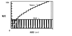
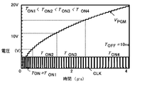
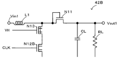
- FIG. It is a circuit diagram which shows the outline of a structure of oscillator 80b, 80c. It is explanatory drawing which shows an example of the time change of the clock signal CLK for control and the voltage Vpass of the output terminal Vout2. It is explanatory drawing which shows an example of the time change of the clock signal for control CLK and the voltage Vpgm of the output terminal Vout3. It is explanatory drawing which shows an example of the boost converter 42B of a modification.
- FIG. 1 is a block diagram showing an outline of a configuration of an SSD (Solid State Disk) 10 as an internal storage device of a computer as an embodiment of the present invention.
- the SSD 10 has a DRAM chip 20 as a silicon chip on which DRAM (Dynamic Random Access Memory) is mounted, a plurality of stacked flash memory chips 22 which are silicon chips on which a NAND flash memory is mounted, and arranged on the top surface.
- the interposer 30 is provided.
- the SSD 10 is supplied with a voltage V0 (for example, 1.6V, 1.8V, 2.0V, etc.) as a power supply voltage from an external power supply (not shown).
- V0 for example, 1.6V, 1.8V, 2.0V, etc.
- the DRAM mounted on the DRAM chip 20 is a DRAM.
- the flash memory mounted on the flash memory chip 22 has a read voltage of the voltage V1 (for example, 9.0V, 10.0V, 11.0V, etc.) and a write voltage of the voltage. V2 (for example, 18V, 20V, 22V, etc.).
- the DRAM chip 20 and the flash memory chip 22 are formed with through holes (not shown) penetrating from the front surface to the back surface of the chip, and the through holes are formed between the DRAM chip 20 and the flash memory chip 22 and are relatively conductive. They are electrically connected by connection wiring formed by embedding with a high metal material (for example, copper).
- FIG. 2 is a circuit diagram for explaining an outline of a configuration of a main part of a NAND flash memory mounted on the flash memory chip 22.
- a drain of a memory cell Mcell having a control gate and a floating gate connected to a word line WL is connected between the bit line BL and the ground GND to the source of the adjacent memory cell Mcell.
- selection MOS transistors ST1 and ST2 having respective gates connected to the selection gate lines SGD and SGS are arranged.
- the voltage V2 is supplied to the word line WL connected to the control gate of the other memory cell Mcell and the selection gate line SGD of the selection MOS transistor ST1, and data corresponding to the voltage of the bit line BL is written. It can be stored in the cell Mcell.
- the interposer 30 boosts the voltage V0 supplied from the NAND controller 32 for controlling the flash memory mounted on the flash memory chip 22 and the power source to the voltage V1 and the voltage V2 and supplies the boosted voltage to the flash memory chip 22.
- a connection wiring (not shown) from the circuit 40, the booster circuit 40 and the NAND controller 32 is mounted.
- FIG. 3 is a circuit diagram showing an outline of the configuration of the booster circuit 40 mounted on the interposer 30.
- the booster circuit 40 boosts the voltage V0 supplied to the input terminal Vin1 and outputs it as the voltage Vmid from the output terminal Vout1, and boosts the voltage supplied to the output terminal Vout1 of the boost converter 42.
- a boost converter 44 that supplies a voltage from Vout2 to the flash memory
- a boost converter 46 that boosts the voltage V0 supplied to the input terminal Vin3 and supplies the voltage from the output terminal Vout3 to the flash memory
- a control clock signal CLK are used.
- a switching control circuit 70 for controlling the boost converters 42, 44, 46.
- An enhancement type NMOS (N-channel Metal Oxide Semiconductor) transistor N11 (hereinafter referred to as transistor N11) and a depletion type connected in parallel to the output terminal Vout1 between the inductor L1 and the transistor N11 as viewed from the inductor L1.
- NMOS transistor N12 hereinafter referred to as transistor N12
- switching of the transistor N12 is controlled by a control clock signal CLK from the switching control circuit 70.
- a smoothing capacitor 42a that smoothes the voltage of the output terminal Vout1 is connected to the output terminal Vout1.
- the transistors N11 and N12 are transistors having a withstand voltage against a voltage slightly higher than a predetermined voltage Vm (eg, 3.6V, 3.8V, 4.0V, etc.) as a voltage between the voltage V0 and the voltage V1. It is configured as.
- Vm a predetermined voltage
- the inductor L2 connected in series between the input terminal Vin2 connected to the output terminal Vout1 of the boost converter 42 and the output terminal Vout2, the gate and the source are connected to each other, and the source is the inductor L2.
- an enhancement type NMOS transistor N21 having a drain connected to the output terminal Vout2 (hereinafter referred to as transistor N21) and an inductor L2 and a transistor N21 connected in parallel to the output terminal Vout2 as viewed from the inductor L2.
- a depletion type NMOS transistor N22 (hereinafter referred to as transistor N22), and switching of the transistor N22 is controlled by a control clock signal CLK from the switching control circuit 70.
- the transistors N21 and N22 are configured as transistors having a threshold voltage higher than that of the transistors N11 and N12 and having a withstand voltage against a voltage slightly higher than the voltage V1.
- the inductor L3 connected in series between the input terminal Vin3 to which the voltage V0 is supplied and the output terminal Vout3, the gate and the source are connected to each other, and the source is connected to the inductor L3.
- An enhancement type NMOS transistor N31 (hereinafter referred to as transistor N31) having a drain connected to the output terminal Vout3, and a depletion type NMOS connected in parallel to the output terminal Vout3 as viewed from the inductor L3 between the inductor L3 and the transistor N31
- a transistor N32 (hereinafter referred to as transistor N32), and switching of the transistor N32 is controlled by a control clock signal CLK from the switching control circuit 70.
- the transistors N31 and N32 are configured as transistors having a threshold voltage higher than those of the transistors N11 and N12 and having a withstand voltage against a voltage slightly higher than the voltage V2.
- the switching control circuit 70 includes a voltage detection circuit 72 that detects the voltage Vmid of the output terminal Vout1 of the boost converter 42, a voltage detection circuit 74 that detects the voltage Vpass of the output terminal Vout2 of the boost converter 44, and an output terminal of the boost converter 46.
- the control clock CLK is an on-time Ton (the control clock signal CLK is a signal of a high-level logic voltage).
- the selection circuit 78a generates a control clock signal CLK that can boost the voltage of the output terminal Vout2 relatively quickly and with low power consumption when the voltage Vmid detected by the voltage detection circuit 72 reaches the voltage Vm.
- the relationship between the on-time Ton and the off-time Toff and the voltage Vpass of the output terminal Vout2 is obtained and stored in advance through experiments or simulations, and the voltage Vmid detected by the voltage detection circuit 72 exceeds the voltage Vm.
- the stored on-time Ton and off-time Toff corresponding to the voltage Vpass detected by the detection circuit 74 are selected and output to the oscillator 80b.
- the selection circuit 78a outputs a standby signal STB to the oscillator 80b when the voltage Vpass detected by the voltage detection circuit 74 exceeds the voltage V1.
- the selection circuit 78b compares the on-time Ton and the off-time Toff of the control clock signal CLK capable of quickly boosting the voltage of the output terminal Vout3 and the elapsed time after the write instruction to write data to the flash memory is made. The relationship is obtained in advance through experiments or simulations and stored in advance, and the stored on-time Ton and off-time Toff are output to the oscillator 80c.
- the ON time Ton of the control clock signal CLK is set so as to increase as the elapsed time after the write instruction to write data to the flash memory is increased, and the OFF time Toff of the control clock signal CLK is the elapsed time. Regardless of what is constant. The reason for setting the on time Ton and the off time Toff in this way will be described later.
- the selection circuit 78b outputs a standby signal STB to the oscillator 80c when the voltage Vpgm detected by the voltage detection circuit 76 exceeds the voltage V2.
- the oscillator 80 a is configured as a well-known oscillator circuit that generates a control clock signal CLK having predetermined on-time and off-time and outputs the clock signal CLK to the transistor N 11 of the boost converter 42, and is detected by the voltage detection circuit 72.
- a control clock signal CLK having a predetermined on time and off time is generated and output to the transistor N12 of the boost converter 42 and detected by the voltage detection circuit 72.
- the control clock signal CLK fixed to a low level logic voltage (for example, 0V) is generated so that the gate of the transistor N11 is turned off, and the boost converter 42 Output to transistor N12.
- FIG. 4 is a circuit diagram showing an outline of the configuration of the oscillators 80b and 80c.
- the oscillators 80b and 80c include a first circuit M1 configured as a constant current circuit, a second circuit M2, a third circuit M3 that forms a current mirror with the first circuit M1, and a first circuit M2, And a clock signal output circuit CKO that generates and outputs a control clock signal CLK from the output of M3.
- the first circuit M1 includes a resistor R and an NMOS transistor NM1 to which the power supply voltage Vdd is supplied to the drain via the resistor R, the gate and the drain are connected, and the source is grounded.
- the second circuits M2 and M3 have the same configuration, and the PMOS (P-channel Metal Oxide Semiconductor) transistor PM1 to which the power supply voltage Vdd is supplied to the source, and the gate and drain of the transistor PM1 are the gate and drain, respectively. And an NMOS transistor NM3 having a gate connected to the gate of the transistor NM1 and a drain connected to the drain of the transistor NM2. Capacitors C1 to C5 are connected in parallel via the switches SW1 to SW5 between the drain of the transistor PM1 of the second circuit M2 and M3 and the ground.
- PMOS P-channel Metal Oxide Semiconductor
- the clock signal output circuit CKO has a reference voltage Vref, which is a voltage between the drain of the transistor NM1 of the first circuit M1 and the ground, and a voltage between the drain of the transistor PM1 of the second circuit M2 and the ground, that is, the capacitor C1.
- the comparator CMP111 that compares the capacitor voltage Vcap1 that is the inter-electrode voltage of .about.C5 and outputs the comparison result, the voltage between the reference voltage Vref and the drain of the transistor PM1 of the third circuit M3 and the ground, that is, the capacitor C1.
- a comparator CMP112 that compares the capacitor voltage Vcap2 that is the inter-electrode voltage of C5 to C5 and outputs a comparison result, and a flip-flop FF that is set or reset in accordance with the comparison results from CMP111 and 112.
- the flip-flop FF is set when the capacitor voltage Vcap1 is equal to or lower than the reference voltage Vref and outputs a low-level logic voltage signal as the control clock signal CLK, and is reset when the capacitor voltage Vcap2 is equal to or lower than the reference voltage Vref.
- a level logic voltage signal is output as a clock signal CLK, and a clock signal CLKB having a phase opposite to that of the control clock signal CLK is also output.
- the oscillators 80b and 80c also include a transistor (not shown) that fixes the voltage of the control clock signal CLK to a low-level logic voltage when the standby signal STB is input from the selection circuits 78a and 78b.
- the ON time Ton and the OFF time Toff of the control clock signal CLK output from the selection circuits 78a and 78b are switched between the resistance value R of the resistor R and the second circuit M2 and the third circuit. Since it is determined by the combined capacitance C of the capacitors connected to the switches that are turned on among SW1 to SW5, the control clock signal CLK for the desired on time and off time is obtained by controlling the on / off of the switches SW1 to SW5. Can be output.
- the booster circuit 40 of the SSD 10 when a read request for reading data from the flash memory mounted on the flash memory chip 22 is made, a boost operation described below is performed.
- a read request when the voltage Vmid of the output terminal Vout1 detected by the voltage detection circuit 72 is equal to or lower than the voltage V1, the oscillator 80a generates a control clock signal CLK having predetermined on-time and off-time. And output to the transistor N12 of the boost converter 42 to control the switching of the transistor N12. Thereby, the voltage Vmid of the output terminal Vout1 can be stepped up.
- the transistor N12 is configured as a transistor having a threshold voltage lower than that of the transistor N22, the voltage Vmid of the output terminal Vout1 is quickly boosted to the voltage Vm as compared with the transistor N22 instead of the transistor N11. can do.
- the selection circuit 78a Based on the detected voltage Vpass, the on time Ton and the off time Toff are selected and output to the oscillator 80b.
- the oscillator 80b generates the control clock signal CLK of the input on time Ton and off time Toff to generate a boost converter.
- the transistor N22 is output to the transistor N22 to control the switching of the transistor N21. Thereby, the voltage Vpass of the output terminal Vout2 can be stepped up in a stepped manner.
- the selection circuit 78a selects the on-time Ton and the off-time Toff that can be boosted relatively quickly and with low power consumption, and outputs the voltage Vpass of the output terminal Vout2 to the oscillator 80b.
- Boosting can be performed relatively quickly and with low power consumption.
- the transistor N22 is configured as a transistor having a higher threshold voltage and higher withstand voltage than the transistor N12, a withstand voltage can be ensured as compared with a transistor using the transistor N12 instead of the transistor N22.
- FIG. 5 shows an example of the time variation of the control clock signal CLK and the voltage Vpass of the output terminal Vout2.
- the selection circuit 78b is based on the detected voltage Vpgm and the ON time Ton of the control clock signal CLK.
- the off time Toff is selected and output to the oscillator 80b.
- the oscillator 80b generates the control clock signal CLK for the input on time Ton and off time Toff and outputs it to the transistor N32 of the boost converter 46 to output the transistor N32. Control switching.
- the reason why the ON time Ton of the control clock signal CLK in the selection circuit 78b is set to become longer as the elapsed time from the request for writing data to the flash memory becomes longer will be described.
- the voltage at the output terminal Vout3 of the boost converter 46 increases, the energy loss of the transistor N32 at the time of boosting increases, and if the on-time of the control clock signal CLK is short, boosting may not be sufficient. Therefore, the voltage Vpgm of the output terminal Vout3 can be sufficiently boosted to the voltage V2 by setting the ON time Ton of the control clock signal CLK so that the elapsed time after the write request is made becomes longer. Because it is considered.
- FIG. 6 shows an example of the time variation of the control clock signal CLK and the voltage Vpgm of the output terminal Vout3.
- the voltage Vpgm of the output terminal Vout3 can be more appropriately boosted to the voltage V2 and supplied to the flash memory 22.
- the oscillator 80a is determined in advance when the voltage Vmid of the output terminal Vout1 detected by the voltage detection circuit 72 is equal to or lower than the voltage V1.
- the on-time and off-time control clock signal CLK is generated and output to the transistor N12 of the boost converter 42 to control the switching of the transistor N12, and the voltage detection circuit indicates that the voltage Vmid of the output terminal Vout1 becomes the voltage Vm.
- the selection circuit 78a selects an on-time Ton and an off-time Toff that can quickly boost the voltage of the output terminal Vout2 with a small amount of power based on the voltage Vpass of the output terminal Vout2, and outputs it to the oscillator 80b.
- Osley 80b are then generates and outputs the control clock signal CLK on time Ton on and off-time Toff which is input to the transistor N22 of the boost converter 44 controls the switching transistor N22.
- the voltage Vpass of the output terminal Vout2 can be stepped up to the voltage V1 stepwise.
- the selection circuit 78b is The on-time Ton and off-time Toff that can quickly boost the stored voltage of the output terminal Vout2 with low power are selected and output to the oscillator 80b.
- the oscillator 80b is a control clock signal for the on-time Ton and off-time Toff.
- CLK is generated and output to the transistor N32 of the boost converter 46 to control the switching of the transistor N32. With such an operation, the voltage Vpgm of the output terminal Vout3 can be more appropriately boosted to the voltage V3 and supplied to the flash memory 22.
- the selection circuit 78a selects an on-time Ton and an off-time Toff that can quickly boost the voltage of the output terminal Vout2 with a small amount of power based on the voltage Vpass of the output terminal Vout2, and outputs it to the oscillator 80b
- the off time Toff is fixed to a certain time, and the on time Ton and the off time Toff time are set so as to become longer as the elapsed time after the read request for reading data from the flash memory becomes longer. It is good also as what outputs to the oscillator 80b. In this way, it is possible to boost the pressure more appropriately.
- the selection circuit 78b is instructed to write data to the flash memory and the on-time Ton and off-time Toff of the control clock signal CLK that can quickly boost the voltage of the output terminal Vout3.
- the relationship with the elapsed time from the time is obtained in advance through experiments or simulations and stored in advance, and the stored on-time Ton and off-time Toff are output to the oscillator 80c.
- the ON time Ton of the control clock signal CLK is set so as to increase as the elapsed time after the write instruction to write data to the flash memory is increased, and the OFF time Toff of the control clock signal CLK is the elapsed time.
- the OFF time Toff may be changed according to the elapsed time together with the ON time Ton.
- the transistors N21 and N22 are configured as transistors having a threshold voltage higher than that of the transistors N11 and N12 and having a withstand voltage against a voltage slightly higher than the voltage V1, but the threshold voltage is higher than that of the transistors N11 and N12. May be a transistor having a high withstand voltage with respect to the voltage V1.
- a transistor having a withstand voltage with respect to the voltage V2 or higher may be used.
- the transistors N31 and N32 are configured as transistors having a threshold voltage higher than those of the transistors N11 and N12 and having a withstand voltage against a voltage slightly higher than the voltage V2.
- the transistors N31 and N32 have a threshold voltage higher than that of the transistors N11 and N12. Any transistor having a withstand voltage with respect to V2 may be used. For example, a transistor having a withstand voltage with respect to a voltage (for example, 30 V) much higher than the voltage V2 may be used.
- the boost converter 42 includes the depletion type NMOS transistor N12 connected in parallel to the output terminal Vout1 when viewed from the inductor L between the inductor L1 and the transistor N11.
- a depletion type NMOS transistor like the boost converter 42B of the modified example illustrated in FIG. 7 may be provided as long as it includes an element that switches with the clock signal CLK in parallel with the output terminal Vout1 as viewed from the inductor L1.
- a depletion type NMOS transistor N13 (hereinafter referred to as transistor N13) connected between the inductor L1 and the transistor N11, and an enhancement type NMOS transistor in series with the transistor N13.
- Njisuta N12B (hereinafter, transistor N12B) assumed to have a, may be used to input control clock signal CLK to the gate of the transistor N12B fixes the voltage of the gate of the transistor N13 to the predetermined voltage VH.
- the predetermined voltage VH is a voltage (for example, 1.8 V) between the voltage V0 and the voltage Vm.
- the boost converter 42 includes the enhancement type NMOS transistor N111 in which the gate and the source are connected to each other, the source is connected to the inductor L1, and the drain is connected to the output terminal Vout1, but the inductor L1 And the output terminal Vout1 are connected in series to rectify the current in the direction from the input terminal Vin1 toward the output terminal Vout1, so that a diode may be provided instead of the transistor N11.
- the boost converter 42 is illustrated, but the boost converters 44 and 46 may be applied to the boost converter of the modified example illustrated in FIG. 7 or the boost converter of another modified example.
- the interposer 30 is arranged on the upper surface of the flash memory chip 22, but it can also be arranged on the lower surface. Further, another integrated circuit chip or an interposer may be stacked on the interposer 30.
- the SSD 10 includes the flash memory chip 22 on which the flash memory is mounted.
- the integrated circuit mounted on the chip is not limited to the flash memory, and is an integrated circuit that operates at a predetermined voltage. It does not matter as long as there is any.
- the present invention is applied to the SSD 10.
- the integrated circuit chip on which the integrated circuit is mounted and the power supply side voltage supplied from the power supply side can be boosted and supplied to the integrated circuit of the integrated circuit chip.
- the integrated circuit device may be used for any device, for example, a microcomputer.
- the flash memory chip 22 corresponds to an “integrated circuit chip”
- the interposer 30 corresponds to an “interposer”
- the booster circuit 40 corresponds to a “boost supply circuit”
- an inductor L1 a transistor N11, a transistor N12, Is equivalent to the “first boost converter”
- the boost converter 44 having the inductor L2 the transistor N21, and the transistor N22 is equivalent to the “second boost converter”
- the switching control circuit 70 is the “switching control circuit”. Is equivalent to.
- the voltage detection circuit 72 corresponds to the “first voltage detection circuit”
- the voltage detection circuit 74 corresponds to the “second voltage detection circuit”
- the voltage Vmid of the output terminal Vout1 detected by the voltage detection circuit 72 and the output Based on the voltage Vpass of the terminal Vout2, the control clock signal CLK is generated and output to the transistor N12 and the transistor N22 to control the transistors N12 and N22, and the oscillators 80a and 80b are connected to the “control clock signal”.
- the boost converter 46 including the inductor L3, the transistor N31, and the transistor N32 corresponds to a “third boost converter”.
- the voltage detection circuit 76 corresponds to a “third voltage detection circuit”, generates a control clock signal CLK based on the voltage at the output terminal Vout3 detected by the voltage detection circuit 76, and outputs the control clock signal CLK to the transistor N31.
- the selection circuit 78b for controlling N31 and the oscillator 80c correspond to a “control clock signal generation circuit”.
- the present invention can be used in the manufacturing industry of integrated circuit devices.
Landscapes
- Engineering & Computer Science (AREA)
- Power Engineering (AREA)
- Dc-Dc Converters (AREA)
Abstract
Description
集積回路が搭載された集積回路チップと、電源側から供給される電源側電圧を昇圧して前記集積回路チップの集積回路に供給可能な昇圧供給回路が搭載されたインターポーザと、を備える集積回路装置であって、
前記昇圧供給回路は、
前記電源側電圧を供給される第1入力端子と電圧を出力する第1出力端子との間に直列に接続された第1インダクタと、前記第1インダクタと前記第1出力端子との間に直列に接続され電流を前記第1入力端子から前記第1出力端子に向かう方向へ整流する第1整流素子と、前記第1インダクタと前記第1整流素子との間に前記第1インダクタからみて前記第1出力端子に並列に接続された第1電界効果トランジスタと、を有する第1ブーストコンバータと、
前記第1ブーストコンバータの第1出力端子の電圧が入力される第2入力端子と前記集積回路チップの集積回路に電圧を供給する第2出力端子との間に直列に接続された第2インダクタと、前記第2インダクタと前記第2出力端子との間に直列に接続され電流を前記第2入力端子から前記第2出力端子に向かう方向へ整流する第2整流素子と、前記第2インダクタと前記第2整流素子との間に前記第2インダクタからみて前記第2出力端子に並列に接続され前記第1電界効果トランジスタより閾値電圧が高く且つ前記集積回路が動作する電圧として予め定められた動作電圧以上の電圧に対して耐圧を有する第2電界効果トランジスタと、を有する第2ブーストコンバータと、
前記第1ブーストコンバータの第1出力端子の電圧が前記動作電圧より低い電圧として予め定められた所定の低電圧以下であるときには前記第1出力端子の電圧が前記所定の低電圧になるよう前記第1ブーストコンバータの第1電界効果トランジスタをスイッチング制御し、前記第1ブーストコンバータの第1出力端子の電圧が前記所定の低電圧に至ったとき以降は前記第2ブーストコンバータの第2出力端子の電圧が前記動作電圧になるよう前記第2ブーストコンバータの前記第2電界効果トランジスタをスイッチング制御するスイッチング制御回路と、
を備える回路であることを要旨とする。
Claims (7)
- 集積回路が搭載された集積回路チップと、電源側から供給される電源側電圧を昇圧して前記集積回路チップの集積回路に供給可能な昇圧供給回路が搭載されたインターポーザと、を備える集積回路装置であって、
前記昇圧供給回路は、
前記電源側電圧を供給される第1入力端子と電圧を出力する第1出力端子との間に直列に接続された第1インダクタと、前記第1インダクタと前記第1出力端子との間に直列に接続され電流を前記第1入力端子から前記第1出力端子に向かう方向へ整流する第1整流素子と、前記第1インダクタと前記第1整流素子との間に前記第1インダクタからみて前記第1出力端子に並列に接続された第1電界効果トランジスタと、を有する第1ブーストコンバータと、
前記第1ブーストコンバータの第1出力端子の電圧が入力される第2入力端子と前記集積回路チップの集積回路に電圧を供給する第2出力端子との間に直列に接続された第2インダクタと、前記第2インダクタと前記第2出力端子との間に直列に接続され電流を前記第2入力端子から前記第2出力端子に向かう方向へ整流する第2整流素子と、前記第2インダクタと前記第2整流素子との間に前記第2インダクタからみて前記第2出力端子に並列に接続され前記第1電界効果トランジスタより閾値電圧が高く且つ前記集積回路が動作する電圧として予め定められた動作電圧以上の電圧に対して耐圧を有する第2電界効果トランジスタと、を有する第2ブーストコンバータと、
前記第1ブーストコンバータの第1出力端子の電圧が前記動作電圧より低い電圧として予め定められた所定の低電圧以下であるときには前記第1出力端子の電圧が前記所定の低電圧になるよう前記第1ブーストコンバータの第1電界効果トランジスタをスイッチング制御し、前記第1ブーストコンバータの第1出力端子の電圧が前記所定の低電圧に至ったとき以降は前記第2ブーストコンバータの第2出力端子の電圧が前記動作電圧になるよう前記第2ブーストコンバータの前記第2電界効果トランジスタをスイッチング制御するスイッチング制御回路と、
を備える回路である
集積回路装置。 - 請求項1記載の集積回路装置であって、
前記スイッチング制御回路は、
前記第1ブーストコンバータの第1出力端子の電圧を検出する第1電圧検出回路と、
前記第2ブーストコンバータの第2出力端子の電圧を検出する第2電圧検出回路と、
前記検出された第1ブーストコンバータの第1出力端子の電圧が前記所定の低電圧以下であるときには予め定められた第1オン時間および第1オフ時間の制御用クロック信号を生成し、前記生成したクロック信号を用いて前記第1電界効果トランジスタをスイッチング制御し、前記検出された第1ブーストコンバータの第1出力端子の電圧が前記所定の低電圧に至ったとき以降は予め定められた第2オン時間および第2オフ時間の制御用クロック信号を生成し、前記生成したクロック信号を用いて前記第2電界効果トランジスタをスイッチング制御する制御用クロック信号生成回路と、
を有する回路である
集積回路装置。 - 請求項1記載の集積回路装置であって、
前記スイッチング制御回路は、
前記第1ブーストコンバータの第1出力端子の電圧を検出する第1電圧検出回路と、
前記第2ブーストコンバータの第2出力端子の電圧を検出する第2電圧検出回路と、
前記検出された第1ブーストコンバータの第1出力端子の電圧が前記所定の低電圧に至ったとき以降は前記検出された第2ブーストコンバータの第2出力端子の電圧が前記動作電圧になるまで前記検出された第1ブーストコンバータの第1出力端子の電圧が前記所定の低電圧に至ってからの経過時間が長くなるほど長くなる傾向に制御用クロック信号のオン時間を設定するオン時間設定回路と、
前記検出された第1ブーストコンバータの第1出力端子の電圧が前記所定の低電圧以下であるときには予め定められた第1オン時間および第1オフ時間の制御用クロック信号を生成し、前記生成したクロック信号を用いて前記第1電界効果トランジスタをスイッチング制御し、前記検出された第1ブーストコンバータの第1出力端子の電圧が前記所定の低電圧に至ったときには前記検出された第2ブーストコンバータの第2出力端子の電圧が前記動作電圧になるまで前記オン時間設定回路により設定されたオン時間および予め定められた第2オフ時間の制御用クロック信号を生成し、前記生成したクロック信号を用いて前記第2電界効果トランジスタをスイッチング制御する制御用クロック信号生成回路と、
を有する回路である
集積回路装置。 - 請求項1記載の集積回路装置であって、
前記電源側電圧から電圧を供給される第3入力端子と前記集積回路チップの集積回路に電圧を出力する第3出力端子との間に直列に接続された第3インダクタと、前記第3インダクタと前記第3出力端子との間に直列に接続され電流を前記第3入力端子から前記第3出力端子に向かう方向へ整流する第3整流素子と、前記第3インダクタと前記第3整流素子との間に前記第3インダクタからみて前記第3出力端子に並列に接続された第3電界効果トランジスタと、を有する第3ブーストコンバータ、を備え、
前記集積回路は、前記動作電圧を第1制御電圧にして動作する第1モードおよび前記動作電圧を前記第1制御電圧より高い第2制御電圧にして動作する第2モードで動作が可能な回路であり、
前記スイッチング制御回路は、前記集積回路を前記第1モードで動作するよう指示がなされたとき、前記第1ブーストコンバータの第1出力端子の電圧が前記所定の低電圧以下であるときには前記第1出力端子の電圧が前記所定の低電圧になるよう前記第1ブーストコンバータの第1電界効果トランジスタをスイッチング制御すると共に前記検出された第1ブーストコンバータの第1出力端子の電圧が前記所定の低電圧に至ったとき以降は前記検出された第2ブーストコンバータの第2出力端子の電圧が前記第1制御電圧になるよう前記第2ブーストコンバータの前記第2電界効果トランジスタをスイッチング制御し、前記集積回路を前記第2モードで動作するよう指示がなされたときには、前記検出された第3ブーストコンバータの第3出力端子の電圧が前記第2制御電圧になるよう前記第3ブーストコンバータの前記第3電界効果トランジスタをスイッチング制御する回路である、
集積回路装置。 - 請求項4記載の集積回路装置であって、
前記スイッチング制御回路は、
前記第1ブーストコンバータの第1出力端子の電圧を検出する第1電圧検出回路と、
前記第2ブーストコンバータの第2出力端子の電圧を検出する第2電圧検出回路と、
前記第3ブーストコンバータの第3出力端子の電圧を検出する第3電圧検出回路と、
経過時間が長くなるほど長くなる傾向に制御用クロック信号のオン時間を設定するオン時間設定回路と、
前記検出された第1ブーストコンバータの第1出力端子の電圧が前記所定の低電圧以下であるときには予め定められた第1オン時間および第1オフ時間の制御用クロック信号を生成し、前記生成したクロック信号を用いて前記第1電界効果トランジスタをスイッチング制御し、前記検出された第1ブーストコンバータの第1出力端子の電圧が前記所定の低電圧に至ったとき以降は予め定められた第2オン時間および第2オフ時間の制御用クロック信号を生成し、前記生成したクロック信号を用いて前記第2電界効果トランジスタをスイッチング制御し、前記検出された第2ブーストコンバータの第2出力端子の電圧が前記第1制御電圧に至ったとき以降は前記検出された第3ブーストコンバータの第3出力端子の電圧が前記第2制御電圧になるまで前記オン時間設定回路により設定されたオン時間および予め定められた第3オフ時間の制御用クロック信号を生成し、前記生成したクロック信号を用いて前記第3電界効果トランジスタをスイッチング制御する制御用クロック信号生成回路と、
を有する回路である
集積回路装置。 - 請求項4または5記載の集積回路装置であって、
前記集積回路チップに搭載されている集積回路は、コントロールゲートとフローティングゲートとを有しコントロールゲートに印加される電圧に応じてデータの読み出しおよび書き込みが可能な複数のフラッシュメモリセルから構成されたNAND型のフラッシュメモリであり、
前記第1モードは、前記NAND型のフラッシュメモリからデータを読み出す読み出し動作を実行するモードであり、
前記第2モードは、前記NAND型のフラッシュメモリにデータを書き込む書き込み動作を実行するモードであり、
前記第1制御電圧は、前記読み出し動作においてデータを読み出すフラッシュメモリセルと異なるフラッシュメモリセルのコントロールゲートに印加される電圧として予め定められた電圧であり、
前記第2制御電圧は、前記書き込み動作においてデータを書き込むフラッシュメモリセルと異なるフラッシュメモリセルのコントロールゲートに印加される電圧として予め定められた電圧である、
集積回路装置。 - 請求項1ないし5いずれか1つの請求項に記載の集積回路装置であって、
前記集積回路チップに搭載されている集積回路は、フラッシュメモリである
集積回路装置。
Priority Applications (2)
| Application Number | Priority Date | Filing Date | Title |
|---|---|---|---|
| JP2013515127A JP5888754B2 (ja) | 2011-05-18 | 2012-05-11 | 集積回路装置 |
| US14/118,464 US9036443B2 (en) | 2011-05-18 | 2012-05-11 | Integrated circuit device |
Applications Claiming Priority (2)
| Application Number | Priority Date | Filing Date | Title |
|---|---|---|---|
| JP2011111660 | 2011-05-18 | ||
| JP2011-111660 | 2011-05-18 |
Publications (1)
| Publication Number | Publication Date |
|---|---|
| WO2012157569A1 true WO2012157569A1 (ja) | 2012-11-22 |
Family
ID=47176887
Family Applications (1)
| Application Number | Title | Priority Date | Filing Date |
|---|---|---|---|
| PCT/JP2012/062175 Ceased WO2012157569A1 (ja) | 2011-05-18 | 2012-05-11 | 集積回路装置 |
Country Status (3)
| Country | Link |
|---|---|
| US (1) | US9036443B2 (ja) |
| JP (1) | JP5888754B2 (ja) |
| WO (1) | WO2012157569A1 (ja) |
Families Citing this family (11)
| Publication number | Priority date | Publication date | Assignee | Title |
|---|---|---|---|---|
| EP2810349B1 (en) * | 2012-02-01 | 2018-06-27 | Schneider Electric IT Corporation | Offline power supply |
| CN106330142B (zh) * | 2015-06-17 | 2023-09-29 | 意法半导体研发(深圳)有限公司 | 时钟相移电路 |
| US10141845B2 (en) | 2016-04-13 | 2018-11-27 | Texas Instruments Incorporated | DC-DC converter and control circuit with low-power clocked comparator referenced to switching node for zero voltage switching |
| US10177658B2 (en) | 2016-04-14 | 2019-01-08 | Texas Instruments Incorporated | Methods and apparatus for adaptive timing for zero voltage transition power converters |
| US10141846B2 (en) * | 2016-04-15 | 2018-11-27 | Texas Instruments Incorporated | Methods and apparatus for adaptive timing for zero voltage transition power converters |
| US10148212B2 (en) * | 2017-01-06 | 2018-12-04 | Thermo King Corporation | DC to DC converter sourcing variable DC link voltage |
| US10003337B1 (en) | 2017-05-17 | 2018-06-19 | International Business Machines Corporation | Resonant virtual supply booster for synchronous logic circuits and other circuits with use of on-chip integrated magnetic inductor |
| US10840797B2 (en) | 2018-11-26 | 2020-11-17 | Texas Instruments Incorporated | Load release detection circuit |
| US10839918B1 (en) * | 2019-06-24 | 2020-11-17 | Sandisk Technologies Llc | Boost converter in memory chip |
| KR102718858B1 (ko) * | 2020-08-26 | 2024-10-17 | 삼성전자주식회사 | 저전력 입출력을 위한 송신기, 수신기 및 이를 포함하는 메모리 시스템 |
| CN120600079B (zh) * | 2025-05-14 | 2026-01-13 | 新存微科技(北京)有限责任公司 | 存储器的外围电路和存储器 |
Citations (3)
| Publication number | Priority date | Publication date | Assignee | Title |
|---|---|---|---|---|
| JP2008071935A (ja) * | 2006-09-14 | 2008-03-27 | Toshiba Corp | 半導体装置 |
| JP2008206317A (ja) * | 2007-02-20 | 2008-09-04 | Institute Of National Colleges Of Technology Japan | 高圧電源回路 |
| WO2010047140A1 (ja) * | 2008-10-20 | 2010-04-29 | 国立大学法人東京大学 | 集積回路装置 |
Family Cites Families (3)
| Publication number | Priority date | Publication date | Assignee | Title |
|---|---|---|---|---|
| JPH0515148A (ja) * | 1991-06-03 | 1993-01-22 | Sony Corp | 電源装置 |
| JP2007102687A (ja) * | 2005-10-07 | 2007-04-19 | Sony Corp | 電源制御装置、電源制御方法、電子機器 |
| JP5709197B2 (ja) * | 2010-05-21 | 2015-04-30 | 国立大学法人 東京大学 | 集積回路装置 |
-
2012
- 2012-05-11 WO PCT/JP2012/062175 patent/WO2012157569A1/ja not_active Ceased
- 2012-05-11 JP JP2013515127A patent/JP5888754B2/ja not_active Expired - Fee Related
- 2012-05-11 US US14/118,464 patent/US9036443B2/en not_active Expired - Fee Related
Patent Citations (3)
| Publication number | Priority date | Publication date | Assignee | Title |
|---|---|---|---|---|
| JP2008071935A (ja) * | 2006-09-14 | 2008-03-27 | Toshiba Corp | 半導体装置 |
| JP2008206317A (ja) * | 2007-02-20 | 2008-09-04 | Institute Of National Colleges Of Technology Japan | 高圧電源回路 |
| WO2010047140A1 (ja) * | 2008-10-20 | 2010-04-29 | 国立大学法人東京大学 | 集積回路装置 |
Also Published As
| Publication number | Publication date |
|---|---|
| US9036443B2 (en) | 2015-05-19 |
| JPWO2012157569A1 (ja) | 2014-07-31 |
| JP5888754B2 (ja) | 2016-03-22 |
| US20140104952A1 (en) | 2014-04-17 |
Similar Documents
| Publication | Publication Date | Title |
|---|---|---|
| JP5888754B2 (ja) | 集積回路装置 | |
| JP5504507B2 (ja) | 集積回路装置 | |
| JP6768776B2 (ja) | フラッシュメモリ装置のハイブリッドチャージポンプ並びに調節手段及び方法 | |
| US9460797B2 (en) | Non-volatile memory cell structure and non-volatile memory apparatus using the same | |
| US7372739B2 (en) | High voltage generation and regulation circuit in a memory device | |
| US20170076800A1 (en) | Voltage generating circuit and semiconductor memory device | |
| US20100124140A1 (en) | Power supply circuit and nand-type flash memory | |
| US20120275226A1 (en) | Nonvolatile semiconductor memory device capable of reducing power consumption | |
| JP5709197B2 (ja) | 集積回路装置 | |
| JP4359319B2 (ja) | 電源回路 | |
| JP6359479B2 (ja) | チャージポンプおよび電圧発生回路 | |
| KR102450890B1 (ko) | 비휘발성 메모리 회로 | |
| JP6298240B2 (ja) | 半導体装置及びその消去方法 | |
| JP5087669B2 (ja) | 電圧発生回路 | |
| US10515669B2 (en) | Voltage generation circuits | |
| JP6164048B2 (ja) | 半導体記憶装置及びそれに用いられる回路装置 | |
| JP2011054735A (ja) | 半導体集積回路装置 | |
| KR101582691B1 (ko) | 플래시 메모리의 바이어스 회로 | |
| JP2009026356A (ja) | データ書き込み方法及び不揮発性半導体記憶装置 | |
| KR20100088924A (ko) | 불휘발성 메모리 장치 |
Legal Events
| Date | Code | Title | Description |
|---|---|---|---|
| 121 | Ep: the epo has been informed by wipo that ep was designated in this application |
Ref document number: 12786758 Country of ref document: EP Kind code of ref document: A1 |
|
| ENP | Entry into the national phase |
Ref document number: 2013515127 Country of ref document: JP Kind code of ref document: A |
|
| NENP | Non-entry into the national phase |
Ref country code: DE |
|
| WWE | Wipo information: entry into national phase |
Ref document number: 14118464 Country of ref document: US |
|
| 122 | Ep: pct application non-entry in european phase |
Ref document number: 12786758 Country of ref document: EP Kind code of ref document: A1 |