WO2012147866A1 - 操作入力装置及び操作入力検出装置 - Google Patents
操作入力装置及び操作入力検出装置 Download PDFInfo
- Publication number
- WO2012147866A1 WO2012147866A1 PCT/JP2012/061249 JP2012061249W WO2012147866A1 WO 2012147866 A1 WO2012147866 A1 WO 2012147866A1 JP 2012061249 W JP2012061249 W JP 2012061249W WO 2012147866 A1 WO2012147866 A1 WO 2012147866A1
- Authority
- WO
- WIPO (PCT)
- Prior art keywords
- coil
- operation input
- input device
- operation unit
- yoke
- Prior art date
- Legal status (The legal status is an assumption and is not a legal conclusion. Google has not performed a legal analysis and makes no representation as to the accuracy of the status listed.)
- Ceased
Links
Images










Classifications
-
- G—PHYSICS
- G06—COMPUTING OR CALCULATING; COUNTING
- G06F—ELECTRIC DIGITAL DATA PROCESSING
- G06F3/00—Input arrangements for transferring data to be processed into a form capable of being handled by the computer; Output arrangements for transferring data from processing unit to output unit, e.g. interface arrangements
- G06F3/01—Input arrangements or combined input and output arrangements for interaction between user and computer
- G06F3/016—Input arrangements with force or tactile feedback as computer generated output to the user
-
- G—PHYSICS
- G01—MEASURING; TESTING
- G01B—MEASURING LENGTH, THICKNESS OR SIMILAR LINEAR DIMENSIONS; MEASURING ANGLES; MEASURING AREAS; MEASURING IRREGULARITIES OF SURFACES OR CONTOURS
- G01B7/00—Measuring arrangements characterised by the use of electric or magnetic techniques
- G01B7/003—Measuring arrangements characterised by the use of electric or magnetic techniques for measuring position, not involving coordinate determination
-
- G—PHYSICS
- G01—MEASURING; TESTING
- G01D—MEASURING NOT SPECIALLY ADAPTED FOR A SPECIFIC VARIABLE; ARRANGEMENTS FOR MEASURING TWO OR MORE VARIABLES NOT COVERED IN A SINGLE OTHER SUBCLASS; TARIFF METERING APPARATUS; MEASURING OR TESTING NOT OTHERWISE PROVIDED FOR
- G01D5/00—Mechanical means for transferring the output of a sensing member; Means for converting the output of a sensing member to another variable where the form or nature of the sensing member does not constrain the means for converting; Transducers not specially adapted for a specific variable
- G01D5/12—Mechanical means for transferring the output of a sensing member; Means for converting the output of a sensing member to another variable where the form or nature of the sensing member does not constrain the means for converting; Transducers not specially adapted for a specific variable using electric or magnetic means
- G01D5/14—Mechanical means for transferring the output of a sensing member; Means for converting the output of a sensing member to another variable where the form or nature of the sensing member does not constrain the means for converting; Transducers not specially adapted for a specific variable using electric or magnetic means influencing the magnitude of a current or voltage
- G01D5/20—Mechanical means for transferring the output of a sensing member; Means for converting the output of a sensing member to another variable where the form or nature of the sensing member does not constrain the means for converting; Transducers not specially adapted for a specific variable using electric or magnetic means influencing the magnitude of a current or voltage by varying inductance, e.g. by a movable armature
- G01D5/2006—Mechanical means for transferring the output of a sensing member; Means for converting the output of a sensing member to another variable where the form or nature of the sensing member does not constrain the means for converting; Transducers not specially adapted for a specific variable using electric or magnetic means influencing the magnitude of a current or voltage by varying inductance, e.g. by a movable armature by influencing the self-induction of one or more coils
- G01D5/2013—Mechanical means for transferring the output of a sensing member; Means for converting the output of a sensing member to another variable where the form or nature of the sensing member does not constrain the means for converting; Transducers not specially adapted for a specific variable using electric or magnetic means influencing the magnitude of a current or voltage by varying inductance, e.g. by a movable armature by influencing the self-induction of one or more coils by a movable ferromagnetic element, e.g. a core
Definitions
- the present invention relates to an operation input device and an operation input detection device including an operation unit on which an operation input acts, and more particularly to an apparatus capable of applying vibration to the operation unit.
- an input device that detects an input position and a pressing force when a user's finger is pressed using a resistive film type touch panel and applies vibration to the touch panel (for example, see Patent Document 1).
- an input position and a pressing force are detected by a voltage measurement circuit, while vibration is given to a user by a vibration motor or the like.
- the function of detecting an operation input acting on the operation unit and the function of applying vibration to the operation unit are realized by separate and independent configurations, and thus the input device is easily increased in size. Also, the configuration for realizing the function of giving vibration is complicated.
- an object of the present invention is to provide an operation input device and an operation input detection device that can realize a function of detecting an operation input acting on the operation unit and a function of applying vibration to the operation unit with a simple configuration.
- an operation input device comprises: Coils, An operation unit that is displaced in the axial direction of the coil by the action of an operation input; A core whose positional relationship with the coil changes due to displacement of the operation unit; A yoke disposed outside the coil; A magnet for generating magnetic flux flowing through the core and the yoke; The coil outputs a signal corresponding to a displacement amount of the operation unit, The operation unit is movable by a current flowing through the coil and a magnetic flux of the magnet.
- an operation input device includes: Coils, An operation unit that is displaced in the axial direction of the coil by the action of an operation input; A core and a yoke whose positional relationship with the coil changes due to the displacement of the operation unit; A magnet disposed between the core and the yoke; The coil outputs a signal corresponding to a displacement amount of the operation unit, The operation unit is movable by a current flowing through the coil and a magnetic flux of the magnet.
- an operation input detection device includes: An operation input device according to the present invention; Detecting means for detecting a change in inductance of the coil; And a control means for moving the operation portion by passing a current through the coil.
- a function of detecting an operation input acting on the operation unit and a function of applying vibration to the operation unit can be realized with a simple configuration.
- FIG. 1 It is a perspective sectional view of operation input device 1 which is a 1st embodiment of the present invention.
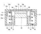
- 2 is a front sectional view of the operation input device 1.
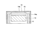
- FIG. It is sectional drawing of the initial position state where the operation input is not provided. It is sectional drawing of the pushing position state to which the operation input is provided. It is explanatory drawing of a magnetic circuit.
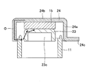
- FIG. 3 is a front sectional view of the operation input device 2.
- FIG. 3 is a front sectional view of a part of the operation input device 2.
- FIG. 3 is a front sectional view of the operation input device 3.
- FIG. It is a perspective sectional view of operation input device 4 which is the 4th embodiment of the present invention.
- 4 is a front sectional view of the operation input device 4.
- FIG. It is a perspective sectional view of operation input device 5 which is a 5th embodiment of the present invention.
- 4 is a front sectional view of the operation input device 5.
- FIG. It is a perspective sectional view of operation input device 6 which is a 6th embodiment of the present invention. 4 is a front sectional view of the operation input device 6.
- An operation input device is an operation interface that receives a force from an operator's finger or the like and outputs an output signal that changes in accordance with the received force.
- An operation input by the operator is detected based on the output signal. By detecting the operation input, it is possible to make the computer grasp the operation content corresponding to the detected operation input.
- an electronic device such as a remote controller for operation of a game machine, a TV, a portable terminal such as a mobile phone or a music player, a personal computer, or an electric appliance
- a display object For example, it is possible to move an instruction display such as a cursor or a pointer or a character according to the operation content intended by the operator.
- an operator gives a predetermined operation input, a desired function of the electronic device corresponding to the operation input can be exhibited.
- the inductance L of an inductor such as a coil (winding) usually has a coefficient K, permeability ⁇ , n number of coil turns, cross-sectional area S, and magnetic path length d.
- L K ⁇ n 2 S / d
- This operation input device receives an operator's force input from a positive Z coordinate direction in an orthogonal coordinate system determined by X, Y, and Z axes.
- the operation input device includes a displacement member that changes the inductance of the coil when the positional relationship with the coil is changed by the action of the operation input.
- the operation input detection device can detect the operation input by detecting the movement of the displacement member that is displaced by the operation input of the operator based on a predetermined signal that changes in accordance with the magnitude of the inductance. .
- the operation input detection device passes a current that generates a magnetic field around the coil to the coil. Due to the magnetic field generated in this manner, a movement that is a stimulus for the operator is generated in the operation unit where the force of the operator can act.
- FIG. 1 is a cross-sectional perspective view of an operation input device 1 according to the first embodiment of the present invention.
- FIG. 2 is a cross-sectional view of the operation input device 1. 1 and 2 illustrate a non-operation state in which an operation input does not act on the operation unit 12. Since the structure of the operation input device 1 is substantially symmetric with respect to the cross section shown in the drawing, the overall view is omitted. The same applies to other operation input devices described later.
- the operation input device 1 includes a coil 11, an operation unit 12, a core 13, a yoke 14, and a magnet 15.
- the coil 11 is formed by winding a wire (conductive wire) into a cylindrical shape.
- the operation unit 12 is a part that is displaced in the axial direction of the coil 11 (vertical direction in the figure) by the action of an operation input.
- the core 13 is a magnetic body whose positional relationship with the coil 11 changes due to the displacement of the operation unit 12.
- the yoke 14 is a magnetic body disposed outside the coil 11.
- the magnet 15 is a source of magnetic flux flowing through the core 13 and the yoke 14.
- the permeability around the coil 11 changes, so the self-inductance of the coil 11 changes.
- the coil 11 outputs a signal waveform corresponding to the amount of displacement of the operation unit 12 according to the change in inductance. Therefore, the displacement amount (operation amount) of the operation unit 12 can be calculated by detecting the signal waveform.
- the operation input device 1 having such a configuration, it is possible to apply vibration of one or more reciprocations to the operation unit 12 only by passing a current through the coil that can detect the displacement amount of the operation unit 12. Therefore, the function of detecting the operation input acting on the operation unit 12 and the function of applying vibration to the operation unit 12 can be realized with a simple configuration.
- the coil 11 is a cylindrical material wound with a wire (conductive wire) and fixed to the base.
- the coil 11 has a cylindrical shape, but may have another cylindrical shape such as a rectangular tube shape.
- 1 and 2 illustrate a configuration in which the coil 11 is wound around and fixed to the outer side surface of the cylindrical portion of the bobbin 18.
- the coil 11 is located between the side surface portion of the columnar core 13 and the side surface portion 14 a of the cylindrical yoke 14.
- the operation unit 12 is configured to continuously change the amount of displacement from the opening of the case 17 to the inside of the case 17 according to the input amount of the operation input acting on the upper operation surface.
- the operation unit 12 is a displacement member that increases the inductance of the coil 2 by being displaced downward in an upper space on the axial extension of the coil 11 by an operation input that directly or indirectly acts on the operation surface.
- the operation unit 12 is provided on the side where an operation input is input to the coil 11, and includes a lower surface facing the upper end surface of the coil 11 and an upper surface on which an operator's force acts directly or indirectly. Have.
- the core 13 is a displacement member that changes the inductance of the coil 11 by displacing the hollow portion of the coil 11 in the axial direction of the coil 11 by the operation input.
- the core 13 is preferably a columnar magnetic body if the coil 11 is cylindrical, and is preferably a prismatic magnetic body if the coil 11 is a rectangular tube.
- the yoke 14 is provided on the upper end surface side of the coil 11, and the positional relationship with the coil 11 changes due to the displacement of the operation unit 12.
- the yoke may be made of a material having a relative permeability higher than 1.
- the relative magnetic permeability is preferably 1.001 or more, specifically, a steel plate (relative magnetic permeability 5000) or the like is preferable.
- the magnet 15 is disposed between the core 13 and the yoke 14 and generates a magnetic flux penetrating the cross section of the core 13 and the cross section of the yoke 14.
- the magnet 15 is formed in a cylindrical shape whose outer diameter is substantially equal to that of the core 13.
- the operation input device 1 is formed with a magnetic circuit including a yoke 14, a magnet 15 having the same movement as the displacement of the yoke 14, and a core 13 made of soft magnetic material.
- the magnet 15 generates a magnetic flux in this magnetic circuit.
- the yoke 14, the magnet 15, the core 13, and the coil 11 are arranged so that the magnetic flux ⁇ generated in the air gap in the magnetic circuit is orthogonal to the axial direction of the coil 11.
- the core 13 is displaced together with the yoke 14 and the magnet 15 due to the displacement of the operation portion 12 due to the operation input. As shown in FIG.
- FIG. 5 is an explanatory diagram of the magnetic circuit.
- the magnet 15 has an outer diameter smaller than the inner diameter of the coil 11 and is end-face magnetized in a magnetization direction D1 that is substantially the same as the operation direction of the operation unit 12.
- the core 13 is disposed on the lower surface 15 b of the magnet 15 and has an outer diameter smaller than the inner diameter of the coil 11.
- the yoke 14 is disposed on the upper surface 15 a of the magnet 15 and has a cup shape in which a cylindrical portion having an inner diameter larger than the outer diameter of the coil 11 is formed.
- the magnet 15, the core 13, and the yoke 14 are displaced in the same downward direction by an operation input acting on the operation unit 12.
- the magnet 15 and the core 13 move in the inner space of the coil 11 in the axial direction of the coil 11, and the side surface portion 14 a of the cylindrical yoke 14 moves in the outer space of the coil 11 along the outer side surface of the coil 11.
- a part of the coil 11 overlaps the side surface portion 14a of the core 13 and the yoke 14 as shown in FIG. 5 in a non-operation state where the operation portion 12 is not operated (initial position state of the operation portion 12). (Overlapping). If they are arranged so as to overlap, a force due to excitation of the coil 11 can be generated from a non-operation state.
- a part of the core 13 and a part of the yoke 14 overlap with a part of the coil 11.
- the lower surface 13 b of the core 13 and the lower end of the side surface portion 14 a of the yoke 14 are positioned below the upper end surface of the coil 11.
- the operation unit 12 can increase the stroke amount by which the inductance can be changed.
- the amount of change in inductance with respect to twelve manipulated variables can be increased, and detection sensitivity can be improved.
- the upper surface 13 a of the core 13 and a part of the side surface portion 14 a of the yoke 14 are located above the upper end surface of the coil 11. That is, the core 13 and the yoke 14 have a portion located above the upper end surface in the axial direction of the coil 11 in a non-operation state.
- the yoke 14 is fixed to the upper surface 15 a of the magnet 15, and the operation unit 12 is fixed in surface contact with the upper surface 14 b of the yoke 14.
- the magnetic flux from the magnet 15 is concentrated in the areas S1 and S2 shown in FIGS. 2 and 5, but if the operating portion 12 is a yoke material (magnetic material) like the yoke 14, the cross-sectional area of the yoke through which the magnetic flux passes is the area. Since it becomes large as shown in S2, the leakage phenomenon due to the magnetic flux saturation of the yoke 14 can be mitigated.
- the operation part 12 is a multistage cup shape in which a plurality of cylindrical parts are formed, as shown in FIG.
- the operation unit 12 has two cylindrical parts, an inner cylindrical part and an outer cylindrical part.
- the side surface portion 12 a of the inner cylindrical portion of the operation portion 12 is fitted into the upper surface opening portion of the case 17 of the operation input device 1, and the side surface portion 12 b of the outer cylindrical portion of the operation portion 12 is fitted to the inner side surface of the cylindrical case 17.
- the case 17 is a housing that houses the operation unit 12.
- the return spring 16 is a support member that elastically supports the operation unit 12 so as to be displaceable in a direction approaching the coil 11.
- the return spring 16 is a coil spring that constantly applies to the operation unit 12 a force in which the operation unit 12 moves away from the coil 11, and the outer cylindrical portion of the operation unit 12 is in contact with the upper surface of the case 17. It is attached in the case 17.
- the return spring 16 is disposed in a cylindrical annular space constituted by the side surface portion 14 a of the yoke 14 and the side surface portion 12 b of the operation unit 12.
- the return spring 16 returns the operating portion 12 to its initial position with initial force on the upper surface of the lower flange of the bobbin 18 and the spring receiving portion 12c of the operating portion 12.
- the spring receiving portion 12 c corresponds to the bottom portion of the outer cylindrical portion of the operation portion 12.
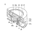
- FIG. 6 is a perspective sectional view of the operation input device 2 according to the second embodiment of the present invention.
- FIG. 7 is a front sectional view of the operation input device 2. The description of the same configurations and effects as those of the above-described embodiment is omitted.
- the operation input device 2 is a cup-shaped core 23 fixed to the lower surface of the magnet 15.
- the core 23 can be formed by press molding or the like, and a concave portion 23 c is formed on the end surface facing the coil 11. Thereby, cost reduction and weight reduction are possible.
- the magnetic flux density of the magnet 15 increases from the central axis of the magnet 15 toward the outer peripheral end. Further, even if the recess 23c is provided as shown in FIG. 8, the gap length between the side surface portion of the core 23 and the side surface portion 24a of the yoke 24 does not change. Therefore, even if the core 23 is cup-shaped, the efficiency of the magnetic circuit and the feedback force that gives vibration to the operation unit 12 can be maintained. Moreover, since the weight of the core 23 which is a movable part can be reduced, the responsiveness of the yoke 24 which has the operation part 24b can be raised. As a result, parts cost reduction and operational feeling (feedback tactile feeling) are improved.
- the yoke 24 can be manufactured by press working or the like. One or more flange portions projecting outward are formed on the side surface portion 24 a of the yoke 24.
- FIG. 9 shows two flange portions 24c and 24d.
- the yoke 24 having the operation surface 24 b rotates around the axial direction of the coil 11 by fitting the flange portion 24 c and the like into the grooves 27 a and 27 b provided in the case 17. Can be stopped. That is, the groove 27 a and the like function as a rotation stop for the yoke 24.
- the operation input device 2 includes a return spring 26 that is disposed inside the coil 11 and has a smaller diameter than the core 23.
- the return spring 26 is fixed to the lower surface of the core 23 and the upper surface of the bottom of the hollow portion of the bobbin 28, and returns the yoke 24 to its initial position with an initial force.
- the lower end of the return spring 26 is positioned by a groove-like spring receiving portion 28 a formed on the upper surface of the bottom of the hollow portion of the bobbin 28, and the upper end of the return spring 26 is positioned by being fitted into the recess 23 c of the core 23. . Since the spring length of the return spring 24 can be increased by using the concave portion 23c of the core 23, various characteristics of the spring such as improved durability and reduced spring rate can be improved.
- FIG. 10 is a perspective sectional view of the operation input device 3 according to the third embodiment of the present invention.
- FIG. 11 is a front sectional view of the operation input device 3. The description of the same configurations and effects as those of the above-described embodiment is omitted.
- the operation input device 3 is a device in which the position of the yoke 34 provided outside the coil 11 is fixed.
- the yoke 34 is a cylindrical member in which a cylindrical portion having an inner diameter larger than the outer diameter of the operation portion 32 that is a yoke material is formed.
- the height of the cylindrical portion of the yoke 34 is from the lower end 11b of the coil 11 to the upper end 32a of the operation portion 32, and is fixed by a case 37A. Since the yoke 34 is not movable while being surrounded by the case 37 and the bobbin 28, the weight of the movable part displaced by the operation input can be reduced, so that the responsiveness when applying the feedback force can be improved.
- the magnet 15 has an outer diameter smaller than the inner diameter of the coil 11, and is end-face magnetized in the magnetization direction D1 substantially the same as the operation direction of the operation unit 32.
- the core 23 is fixed to the lower surface 15 b of the magnet 15 and is smaller than the inner diameter of the coil 11.
- the operation unit 32 is a disk-shaped member that is fixed to the upper surface 15a of the magnet 15 and has an upper surface 32a on which an operation input acts.
- the case 37B is a stopper for the operation unit 32.
- the magnet 15 and the core 23 are displaced in the same direction downward by an operation input acting on the operation unit 32. Even if the magnet 15 and the core 23 move in the inner space of the coil 11 in the axial direction of the coil 11 and the operation portion 32 is displaced, the cylindrical yoke 34 does not move.
- FIG. 12 is a perspective sectional view of the operation input device 4 according to the fourth embodiment of the present invention.
- FIG. 13 is a front sectional view of the operation input device 4. The description of the same configurations and effects as those of the above-described embodiment is omitted.
- the operation input device 4 is a device in which the coil 11 is displaced without displacement of the magnetic circuit portion composed of the core 13, the yoke 14, and the magnet 15 due to the displacement of the operation unit 48. Responsiveness when applying a feedback force can be improved by using a core, yoke, or magnet mainly composed of iron as a fixed part instead of a movable part.
- the operation unit 48 also functions as a bobbin for the coil 11. This configuration can also be applied to other operation input devices of the present application, for example.
- FIG. 14 is a perspective sectional view of the operation input device 5 according to the fifth embodiment of the present invention.
- FIG. 15 is a front sectional view of the operation input device 5. The description of the same configurations and effects as those of the above-described embodiment is omitted.
- a cylindrical magnet 55 in which a cylindrical portion having an outer diameter smaller than the inner diameter of the coil 11 is formed generates magnetic flux in the magnetic circuit.
- the cylindrical portion of the magnet 55 is end-face magnetized in a magnetization direction D2 substantially perpendicular to the operation direction of the operation unit 12 (the axial direction of the coil 11).
- the core 53 is formed in a columnar shape, and is fitted and fixed inside the cylindrical portion of the magnet 55.
- the magnet 55, the core 53, and the yoke 14 are displaced in the same downward direction by an operation input that acts on the operation unit 12.
- the magnet 55 and the core 53 move in the inner space of the coil 11 in the axial direction of the coil 11, and the side surface portion 14 a of the cylindrical yoke 14 moves in the outer space of the coil 11 along the outer side surface of the coil 11.
- FIG. 16 is a perspective sectional view of the operation input device 6 according to the sixth embodiment of the present invention.
- FIG. 17 is a front sectional view of the operation input device 6. The description of the same configurations and effects as those of the above-described embodiment is omitted.
- a cylindrical magnet 65 in which a cylindrical portion having an inner diameter larger than the outer diameter of the coil 11 is formed generates magnetic flux in the magnetic circuit.
- the cylindrical portion of the magnet 65 is end-surface magnetized in a magnetization direction D2 that is substantially perpendicular to the operation direction of the operation unit 12 (the axial direction of the coil 11).
- the cylindrical magnet 65 is fitted and fixed inside the side surface of the cup-shaped yoke 14.
- the core 63 is formed in a columnar shape, is fixed to the lower surface of the yoke 14, and is slidably fitted inside the cylindrical portion of the bobbin 18.
- the yoke 14 is a cylindrical member having an inner diameter larger than the outer diameter of the coil 11 and larger than the outer diameter of the cylindrical magnet 65.
- the magnet 65, the core 63, and the yoke 14 are displaced downward in the same manner by an operation input that acts on the operation unit 12.
- the core 53 moves in the inner space of the coil 11 in the axial direction of the coil 11, and the cylindrical portion of the magnet 65 and the side surface portion 14 a of the cylindrical yoke 14 move in the outer space of the coil 11 along the outer side surface of the coil 11.
- the cylindrical magnet 65 may be divided into several pieces.
- the detection unit is a detection unit that outputs a detection signal corresponding to the continuously changing analog displacement of the operation unit by electrically detecting a change in the inductance of the coil.
- the detection unit may be configured by a detection circuit mounted on a substrate (not shown).
- the detection unit detects a physical quantity that changes equivalently to a change in the inductance of the coil, and outputs the detected value of the physical quantity as a value equivalent to the displacement amount of the operation unit.
- the detection unit may calculate the inductance of the coil by detecting a physical quantity that changes equivalently to the change in the inductance of the coil, and output the calculated value of the inductance as a value equivalent to the displacement of the operation unit. Good.
- the detection unit may calculate the displacement amount of the operation unit from the detected value of the physical quantity or the calculated value of the inductance, and output the calculated value of the displacement amount.
- the detection unit supplies a pulse signal to the coil to generate a signal waveform that changes in accordance with the magnitude of the inductance of the coil, and changes the inductance of the coil based on the signal waveform. Is preferably detected electrically.
- the detection unit detects the amplitude and sets the detected value of the amplitude as a value equivalent to the displacement amount of the operation unit. Can be output.
- the detection unit can also calculate the inductance of the coil from the detected value of the amplitude, and output the calculated value of the inductance as a value equivalent to the displacement amount of the operation unit.
- the detection unit detects the inclination and sets the detected value of the inclination as a value equivalent to the displacement amount of the operation unit. Can be output.
- the detection unit can also calculate the inductance of the coil from the detected value of the tilt, and output the calculated value of the inductance as a value equivalent to the displacement amount of the operation unit.
- the detecting unit is, for example, a detecting unit that detects a change in the inductance of the coil by supplying a first pulse signal to the coil.
- the detection unit supplies a pulse current (first pulse current) corresponding to the first pulse signal to the coil, and based on a pulse voltage (first pulse voltage) generated at both ends of the coil, the inductance of the coil Detect changes.
- the displacement amount of the operation unit can be calculated according to the detection result of the change in the inductance of the coil.
- control unit is a control unit that generates, for example, a magnetic field that moves the operation unit by supplying a second pulse signal having a phase different from that of the first pulse signal to the coil.
- a magnetic field generated by a pulse current (second pulse current) corresponding to the second pulse signal flowing through the coil generates a force that pulls the operation unit to and from the coil together with the core.
- the operation unit is vibrated by fluctuations in the magnitude of the force generated when the second pulse signal is supplied to the coil. That is, since the second pulse signal is a signal whose amplitude temporarily changes, the magnitude of the force applied to the operation unit can be varied.
- the first pulse signal and the second pulse signal may be a rectangular wave, a triangular wave, or a sawtooth wave.
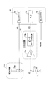
- FIG. 18 is a block diagram of a first example of a control circuit including a detection unit that detects a change in inductance and a control unit that moves the operation unit.
- the control circuit is calculation means for detecting a change in inductance of the coil L.
- the control circuit is connected to an arithmetic circuit 70 such as a CPU, a drive circuit 76 connected to the first output port 71 of the arithmetic circuit 70, and a second output port 72 and an AD port 73 of the arithmetic circuit 70.
- a receiving circuit 77 The coil L is connected to the arithmetic circuit 60 via the receiving circuit 77 and the driving circuit 76.
- the drive circuit 76 controls the output current of the constant current source 76a in accordance with the output signal from the output port 71 of the arithmetic circuit 70, thereby causing a current to flow through the coil L.
- the receiving circuit 77 inputs a voltage generated when a current flows through the coil L to the peak hold circuit 77b through the amplifier 77a (may be input to the bottom hold circuit).
- the peak value (analog value) peak-held by the peak hold circuit 77b is input to the AD port 73 and converted into a digital value by the AD converter.
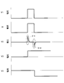
- FIG. 19 is a diagram showing waveforms at each point in FIG.
- a rectangular wave voltage waveform is output from the output port 71 of the arithmetic circuit 70.
- the constant current circuit 76a passes a constant current through the coil.
- the coil generates a voltage V2 having a differential waveform.
- As the voltage waveform V2 a waveform 2-1 synchronized with the rising of the voltage waveform V1 is obtained, and a waveform 2-2 synchronized with the falling of the voltage waveform V1 is obtained.
- the waveform 2-2 is a waveform having positive and negative sides opposite to the waveform 2-1.
- the amplifier 77a amplifies the voltage waveform V2 to a size suitable for the dynamic range of the AD converter.
- the held value is taken into the AD converter (AD port 73). Since the amplitude values of the waveforms 2-1 and 2-2 increase in proportion to the magnitude of the inductance of each coil, the magnitude of the inductance of each coil can be evaluated by detecting this amplitude value.
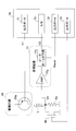
- FIG. 20 is a block diagram of a second example of a control circuit including a detection unit that detects a change in inductance and a control unit that moves the operation unit.
- the driving circuit 86 applies a constant voltage output to the coil L by controlling the transistor 86a according to the output signal from the output port 71 of the arithmetic circuit 70.
- a resistor R1 is connected between the operation detection coil L and the ground, and a low-pass filter is formed by the coil L and the resistor R1.
- a voltage V4 (a voltage across the resistor R1) generated between the coil L and the resistor R1 is input to the peak hold circuit 77b via the amplifier 77a.
- the peak value (analog value) peak-held by the peak hold circuit 77b is input to the AD port 73 and converted into a digital value by the AD converter.
- the switch element 88 connected in parallel with the resistor R1 is off when a pulse for detecting the displacement amount of the operation unit is applied.
- the switch element 88 is turned on in synchronization with the application of the feedback pulse in accordance with the output signal from the output port 74 of the arithmetic circuit 70.
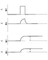
- FIG. 21 is a diagram showing waveforms at each point in FIG.
- a rectangular wave voltage waveform is output from the output port 71 of the arithmetic circuit 70.
- the drive circuit 86 applies a constant voltage to the coil L.
- a voltage waveform V4 as shown is generated.
- the amplifier 77a amplifies such a voltage waveform V4 to a size suitable for the dynamic range of the AD converter.
- the held value is taken into the AD converter (AD port 73). Since the amplitude value of the voltage waveform V3 decreases in inverse proportion to the inductance of the coil L, the magnitude of the inductance of the coil can be evaluated by detecting this amplitude value.
- FIG. 22 is a block diagram of a third example of the control circuit including a detection unit that detects a change in inductance and a control unit that moves the operation unit.
- the resistor R1 is set to have a smaller variation error of the resistance value with respect to the temperature than the internal resistance (resistance component) of the coil L.
- the resistance value increases due to the temperature rise of the internal resistance of the coil L, and the voltage waveform V4 when the rectangular wave is applied to the coil L is evaluated. Can be detected.
- the inductance of the coil L is 0.6 mH when the operation unit is in the initial position, and 1.0 mH when the operation unit is pushed down to the maximum.
- the time constant of the filter constituted by the coil L and the resistance R1 is 1.28 ⁇ sec.
- the applied voltage V5 output from the drive circuit 86 is 3V and the internal resistance of the coil L is set to 15 ⁇
- the voltage waveform V3 at the initial position of the operation unit is about 2.33V, which is the maximum displacement of the operation unit.
- the voltage waveform V3 is about 1.77V.
- the push amount of the operation unit can be detected by detecting the voltage waveform V3.
- the resistance element exists from one having a large temperature characteristic to one having a small temperature characteristic. % / ° C. is also readily available.
- the coil L when an element having a resistance temperature characteristic of 0.4% / ° C. is used as the coil L and an element having a resistance temperature characteristic of 0.01% / ° C. is used as the resistor R1, the coil The voltage value of the voltage V3 when the heating upper limit value of the internal temperature of L is 100 ° C. is reduced to 2.88V with respect to 2.91V at room temperature.
- the pulse signal output method to the coil L is changed or stopped. Thereby, before the internal temperature of the coil L exceeds an allowable range, damage to the coil L and the like can be prevented in advance.
- the switch element 88 is an element for decreasing the impedance when applying the feedback pulse and increasing the value of the current flowing through the coil L.
- an element having a resistance value of 2 ⁇ and a temperature characteristic of the resistance value of 0.01% / ° C. is used as the resistance R2, the resistance value of the internal resistance is 15 ⁇ , and the temperature characteristic of the resistance value is 0. Assuming that the element of 4% / ° C.
- the voltage difference between the voltage V3 at a room temperature of 25 ° C. and the voltage V3 at a high temperature of 100 ° C. is 30 V with respect to the voltage difference when the resistor R2 is not provided. Therefore, the detection error of the voltage difference can be suppressed.
- FIG. 23 is a waveform diagram when the operation input device is operated.
- the operation control method of the operation input device includes an inductance detection step of detecting a change in the inductance of the coil L by supplying a first pulse signal to the coil L.
- the in arithmetic circuit 70 has a pulse waveform corresponding to the first pulse signal supplied to the coil L from the output port 71 as a rectangular wave voltage waveform V1, as shown in FIG. p (p1 to p9) is output.
- the pulse waveform p is intermittently output from the output port 71 to the coil L, whereby the first pulse signal is intermittently supplied to the coil L.
- the pulse waveforms p1 to p9 of the voltage waveform V1 are output at a constant cycle.
- the pulse waveform p is a drive voltage for detecting a change in the inductance of the coil L.
- the detection voltage V3 accompanying the increase in inductance is generated by the drive voltage V1 in accordance with the pressing amount W of the operation unit shown in (a).
- the amplitude of the detection voltage V3 also increases in proportion to the pressing amount W.
- the amplitudes of the pulse waveforms s3, s4, and s5 of the detection voltage V3 increase with the increase of the push amount W, and the amplitudes of the pulse waveforms s6 and s7 of the detection voltage V3 decrease with the decrease of the press amount W.
- the amplitude of the pulse waveform of the detection voltage V3 is the same (s1, s2, s8, s9).
- the operation control method of the operation input device is such that a second pulse signal having a phase different from that of the first pulse signal supplied in the inductance detection step is supplied to the coil L, so that the operation unit is moved to the core or yoke.
- the arithmetic circuit 70 has a pulse waveform q corresponding to the second pulse signal supplied to the coil L as a rectangular wave voltage waveform V1 from the output port 71 as shown in FIG. (Q1 to q5) are output.
- the pulse waveform q is output from the output port 71 to the coil L, whereby the second pulse signal is supplied to the coil L.
- a force F that attracts the operating portion to the coil L side is generated.
- FIG. 23 shows a control method for outputting the pulse waveforms q1 to q5 according to the amplitude of the detection voltage V3, which is the detection result of the change in inductance. That is, when the detection voltage V3 has an amplitude less than a predetermined threshold, the pulse waveform q is not output. When the detection voltage V3 having an amplitude greater than or equal to the predetermined threshold occurs, the pulse waveform q corresponding to the amplitude of the detection voltage V3. Is output. That is, the pulse waveform q that generates the displacement of the operation unit in accordance with the pressing amount W is generated with an amplitude proportional to the amplitude of the detection voltage V3. Then, a suction force F having a magnitude corresponding to the amplitude of the pulse waveform q is generated.
- the amplitude voltage, pulse width, and output period of the pulse waveform p for detecting the change in inductance need only be large enough to detect the change in inductance by the detection voltage V3, and the displacement of the operation unit that can be sensed by the operator. It is sufficient that the magnetic field H is large enough not to be generated. Thereby, it is possible to prevent the operator from feeling the displacement of the operation unit every time the change in inductance is detected.
- the amplitude voltage, the pulse width, and the period of the pulse waveform q are determined by the displacement of the operation unit that can be sensed by the operator so that the operator can reliably detect the displacement of the operation unit that accompanies the pulse waveform q. As long as the magnetic field H can be generated, the size of the magnetic field H may be sufficient. For example, at least one of the amplitude voltage and the pulse width of the pulse waveform q is made larger than the pulse waveform p.
- the arithmetic circuit 70 erroneously detects the detection voltage V3 generated by outputting the pulse waveform q for giving displacement to the operation unit as a signal representing a change in inductance.
- a reset signal VR for preventing the reception circuit 77 from operating may be generated at least in a period in which the pulse waveform q is generated. Thereby, it is possible to prevent the detection voltage V3 from being generated as shown in (c) during the period in which the pulse waveform q is output.
- the arithmetic circuit 70 Since the pulse waveform q is output by the arithmetic circuit 70 itself, the arithmetic circuit 70 does not evaluate (ignore) the detection voltage V3 generated along with the pulse waveform q as a signal representing a change in inductance. May be.
- (b) shows a control method in which a pulse waveform q having an amplitude corresponding to the magnitude of the push-down amount W is output, but as shown in (f), it depends on the magnitude of the push-down amount W.
- a control method for outputting the pulse waveform q having a pulse width to displace the operation unit may be used. As the push-down amount W increases, the pulse width of the pulse waveform q is increased.
- a control method may be used in which the number of pulse waveforms q corresponding to the amount of push-down amount W is output to displace the operation unit. As the push-down amount W increases, the number of pulse waveforms q is increased.
- the pulse waveform q Is not necessarily synchronized with the pulse waveform p
- the time interval for generating the pulse waveform q (the output interval of the pulse waveform q) may be changed across the plurality of pulse waveforms p.
- the pulse waveform p for detecting the change in inductance corresponds to the temporal resolution (follow-up speed) of detecting the change in inductance, and is preferably output at a short time interval.
- the pulse waveform q for imparting displacement to the operation unit needs to make the operator feel that the displacement of the operation unit has occurred, so the output interval is made longer than the pulse waveform p.
- the pulse waveform q may be output during an arbitrary period in which the pulse waveform p is not output so as not to overlap with the pulse waveform p.
- the pulse waveform q is prioritized over the pulse waveform p, and the pulse waveform is output during the output period of the pulse waveform q.
- the output of p may be stopped.
- the displacement of the operation unit according to the push-down amount W is generated.
- the supply mode of the pulse waveform q the flow of current flowing in the coil changes, so that the operator
- the mode of vibration applied to the can be changed. For example, it is possible to change the strength of vibration, the vibration frequency, and the number of vibrations given to the operator by changing the flow of current flowing through the coil by changing the supply mode of the second pulse signal.
- the occurrence timing of the displacement of the operation unit is not limited to change according to the push-down amount W, but the push-down speed of the operation unit and the object that moves by the operation of the operation unit (for example, a cursor on the display, a pointer, etc.)
- the movement position and the operation input device may be changed according to the occurrence of an event on the application used. For example, when the pressing amount W of the operating unit reaches a predetermined value, a magnetic field that displaces the operating unit is generated by supplying the second pulse signal to the coil. Thus, the operator can feel a click feeling due to the displacement generated in the operation unit.
- vibration can be generated simply by applying an applied voltage to the coil for detecting the inductance for feedback.
- the detection function of the operation unit and the vibration generation function can be realized only by changing the frequency, voltage, interval, and the like of the waveform output from the drive circuit of the detection circuit unit for detecting the inductance.
- the configuration is extremely simple, and no additional actuator is required.
- the method of vibrating the entire product including an operation input device such as a vibration motor can be changed only by the strength and time for vibrating the entire product.
- the change of force can be directly output to an operation part. Therefore, for example, if a plurality of operation input devices are mounted, feedback can be output (vibrated) for each operation unit.
- a direct tactile sensation can be given.
- the vibration motor needs to increase the rotation speed in order to increase the vibration amplitude, and it takes time until the rotation increases, so the response is low and the vibration frequency and amplitude cannot be controlled individually.
- the force is output only to the relatively light part of the operation unit, so that the tactile sensation such as a click feeling is output with one pulse by changing the output pulse.
- the tactile sensation like vibration by repeating pulses.
- the amplitude, frequency, pulse width, and the like can be freely changed, the tactile sensation can be changed as necessary.
- the support member that elastically supports the operation unit is not limited to an elastic member such as a return spring, but may be a rubber member, a sponge member, or a cylinder filled with air or oil.
- the operation input device of the present invention is not limited to fingers and may be operated with the palm of the hand. Moreover, you may operate with a toe or a sole.
- the surface touched by the operator may be a flat surface, a concave surface, or a convex surface.
- Operation input device 11 Coil 11a Upper end 11b Lower end 12 Operation unit (yoke) 12a, 12b Side surface portion 12c Spring receiving portion 13 Core 13a Upper surface 13b Lower surface 14 Yoke 14a Side surface portion 14b Upper surface 15 Magnet 15a Upper surface 15b Lower surface 16 Return spring 17 Case 17a Groove 18 Bobbin 18a Spring receiving portion 23 Core 23b Lower surface 23c Recessed portion 23c Surface 24 York 24a Side surface 24b Operation surface (operation unit) 24c, 24d Flange part 26
Landscapes
- Engineering & Computer Science (AREA)
- Physics & Mathematics (AREA)
- General Physics & Mathematics (AREA)
- General Engineering & Computer Science (AREA)
- Theoretical Computer Science (AREA)
- Human Computer Interaction (AREA)
- Position Input By Displaying (AREA)
- Electromagnets (AREA)
- Measurement Of Length, Angles, Or The Like Using Electric Or Magnetic Means (AREA)
Abstract
コイル11と、操作入力の作用によりコイル11の軸方向に変位する操作部12と、操作部12の変位により、コイル11との位置関係が変化するコア13と、コイル11の外側に配置されたヨーク14と、コア13とヨーク14に流れる磁束を発生させるマグネット15とを有し、コイル11は、操作部12の変位量に応じた信号を出力し、操作部12は、コイル11に流れる電流とマグネット15の磁束によって可動する、ことを特徴とする、操作入力装置。
Description
本発明は、操作入力が作用する操作部を備える操作入力装置及び操作入力検出装置に関し、より詳細には、操作部に振動を与えることが可能なものに関する。
従来、抵抗膜方式のタッチパネルを用いて使用者の指の押圧時の入力位置及び押圧力を検知するとともに、タッチパネルに振動を与える入力装置が知られている(例えば、特許文献1参照)。この入力装置では、電圧測定回路によって入力位置及び押圧力を検知する一方で、振動モータなどによって使用者に対して振動を与えている。
しかしながら、上述の従来技術では、操作部に作用する操作入力を検出する機能と操作部に振動を与える機能を別々の独立した構成で実現しているため、入力装置が大型化しやすい。また、振動を与える機能を実現するための構成も複雑である。
そこで、本発明は、操作部に作用する操作入力を検出する機能と操作部に振動を与える機能を単純な構成で実現できる、操作入力装置及び操作入力検出装置の提供を目的とする。
上記目的を達成するため、本発明に係る操作入力装置は、
コイルと、
操作入力の作用により前記コイルの軸方向に変位する操作部と、
前記操作部の変位により、前記コイルとの位置関係が変化するコアと、
前記コイルの外側に配置されたヨークと、
前記コアと前記ヨークに流れる磁束を発生させるマグネットとを備え、
前記コイルは、前記操作部の変位量に応じた信号を出力し、
前記操作部は、前記コイルに流れる電流と前記マグネットの磁束によって可動する、ことを特徴とするものである。
コイルと、
操作入力の作用により前記コイルの軸方向に変位する操作部と、
前記操作部の変位により、前記コイルとの位置関係が変化するコアと、
前記コイルの外側に配置されたヨークと、
前記コアと前記ヨークに流れる磁束を発生させるマグネットとを備え、
前記コイルは、前記操作部の変位量に応じた信号を出力し、
前記操作部は、前記コイルに流れる電流と前記マグネットの磁束によって可動する、ことを特徴とするものである。
また、上記目的を達成するため、本発明に係る操作入力装置は、
コイルと、
操作入力の作用により前記コイルの軸方向に変位する操作部と、
前記操作部の変位により、前記コイルとの位置関係が変化するコア及びヨークと、
前記コアと前記ヨークとの間に配置されたマグネットとを有し、
前記コイルは、前記操作部の変位量に応じた信号を出力し、
前記操作部は、前記コイルに流れる電流と前記マグネットの磁束によって可動する、ことを特徴とするものである。
コイルと、
操作入力の作用により前記コイルの軸方向に変位する操作部と、
前記操作部の変位により、前記コイルとの位置関係が変化するコア及びヨークと、
前記コアと前記ヨークとの間に配置されたマグネットとを有し、
前記コイルは、前記操作部の変位量に応じた信号を出力し、
前記操作部は、前記コイルに流れる電流と前記マグネットの磁束によって可動する、ことを特徴とするものである。
また、上記目的を達成するため、本発明に係る操作入力検出装置は、
本発明に係る操作入力装置と、
前記コイルのインダクタンスの変化を検出する検出手段と、
前記コイルに電流を流すことによって、前記操作部を可動させる制御手段とを備えることを特徴とするものである。
本発明に係る操作入力装置と、
前記コイルのインダクタンスの変化を検出する検出手段と、
前記コイルに電流を流すことによって、前記操作部を可動させる制御手段とを備えることを特徴とするものである。
本発明によれば、操作部に作用する操作入力を検出する機能と操作部に振動を与える機能を単純な構成で実現できる。
以下、図面を参照しながら、本発明を実施するための形態の説明を行う。本発明の一実施形態である操作入力装置は、操作者の手指等による力を受けて、その受けた力に応じて変化する出力信号を出力する操作インターフェイスである。その出力信号に基づいて操作者による操作入力が検出される。操作入力の検出によって、その検出された操作入力に対応する操作内容をコンピュータに把握させることができる。
例えば、ゲーム機、テレビ等の操作用リモートコントローラ、携帯電話や音楽プレーヤーなどの携帯端末、パーソナルコンピュータ、電化製品などの電子機器において、そのような電子機器に備えられるディスプレイの画面上の表示物(例えば、カーソルやポインタなどの指示表示や、キャラクターなど)を、操作者が意図した操作内容に従って、移動させることができる。また、操作者が所定の操作入力を与えることにより、その操作入力に対応する電子機器の所望の機能を発揮させることができる。
一方、通常、コイル(巻線)等のインダクタのインダクタンスLは、係数をK、透磁率をμ、コイルの巻数をn、断面積をS、磁路長をdとした場合、
L=Kμn2S/d
という関係式が成り立つ。この関係式から明らかなように、コイルの巻数や断面積といった形状に依存するパラメータを固定した場合、周囲の透磁率と磁路長の少なくともいずれかを変化させるかによって、インダクタンスが変化する。
L=Kμn2S/d
という関係式が成り立つ。この関係式から明らかなように、コイルの巻数や断面積といった形状に依存するパラメータを固定した場合、周囲の透磁率と磁路長の少なくともいずれかを変化させるかによって、インダクタンスが変化する。
このインダクタンスの変化を利用する操作入力装置及び操作入力検出装置の実施例について以下説明する。この操作入力装置は、X,Y,Z軸によって定まる直交座標系において、正のZ座標の方向から入力される操作者の力を受け付けるものである。操作入力装置は、操作入力の作用によりコイルとの位置関係が変化することによって、そのコイルのインダクタンスを変化させる変位部材を備えている。操作入力検出装置は、そのインダクタンスの大きさに応じて変化する所定の信号に基づいて、操作者の操作入力により変位する変位部材の動きを検知することにより、その操作入力を検出することができる。
また、操作入力検出装置は、コイルの周囲に磁界を発生させる電流をそのコイルに流す。このように発生した磁界によって、操作者の刺激となる動きを、操作者の力が作用しうる操作部に生じさせるものである。
図1は、本発明の第1の実施形態である操作入力装置1の断面斜視図である。図2は、操作入力装置1の断面図である。図1,2は、操作入力が操作部12に作用していない非操作状態を示している。操作入力装置1の構造は、図示の断面に対して略対称であるため、全体図については省略する。後述の他の操作入力装置についても同様である。
操作入力装置1は、コイル11と、操作部12と、コア13と、ヨーク14と、マグネット15とを備えている。コイル11は、線材(導線)が筒状に巻かれて形成されている。操作部12は、操作入力の作用によりコイル11の軸方向(図の場合、上下方向)に変位する部位である。コア13は、操作部12の変位により、コイル11との位置関係が変化する磁性体である。ヨーク14は、コイル11の外側に配置された磁性体である。マグネット15は、コア13とヨーク14に流れる磁束の発生源である。
操作部12の変位によりコイル11とコア13との位置関係が変化すると、コイル11周辺の透磁率が変化するため、コイル11の自己インダクタンスが変化する。コイル11は、そのインダクタンスの変化に応じて、操作部12の変位量に応じた信号波形を出力する。したがって、その信号波形を検出することによって、操作部12の変位量(操作量)を算出できる。
また、コイル11に電流を流すと、コイル11に流れる電流に応じて発生する磁束とマグネット15から発生する磁束によってコア13に力が働くため、コア13に働く力に応じて変位する操作部12を動かすことができる。
したがって、このような構成を有する操作入力装置1によれば、操作部12の変位量を検出可能にするコイルに電流を流すだけで、操作部12に一又は二往復以上の振動を与えることができるので、操作部12に作用する操作入力を検出する機能と操作部12に振動を与える機能を単純な構成で実現できる。
次に、操作入力装置の構成について更に詳細に説明する。
コイル11は、円筒状に線材(導線)が巻かれて、基部に固定されたものである。コイル11は、円筒状であるが、角筒状等の他の筒状の形状でもよい。図1,2には、コイル11が、ボビン18の円筒部の外側側面に巻き回されて固定されている構成が例示されている。コイル11は、円柱状のコア13の側面部と円筒状のヨーク14の側面部14aとの間に位置する。
操作部12は、その上側の操作面に作用する操作入力の入力量に応じて、ケース17の開口部からケース17の内方への変位量が連続的に変化するものである。操作部12は、操作面に直接又は間接的に作用する操作入力により、コイル11の軸方向延長上の上方空間において下方に変位することによって、コイル2のインダクタンスを増加させる変位部材である。操作部12は、コイル11に対して操作入力が入力されてくる側に設けられており、コイル11の上端面に対向する下面と、操作者の力が直接又は間接的に作用する上面とを有している。
コア13は、操作入力の作用によりコイル11の中空部をコイル11の軸方向に変位することによって、コイル11のインダクタンスを変化させる変位部材である。コア13は、コイル11が円筒状であれば、円柱状の磁性体であることが好ましく、コイル11が角筒状であれば、角柱状の磁性体であることが好ましい。
ヨーク14は、コイル11の上端面側に設けられ、操作部12の変位によりコイル11との位置関係が変化する。ヨークは、比透磁率が1よりも高い材質であればよい。例えば、比透磁率は1.001以上あると好適であり、具体的には、鋼板(比透磁率5000)などが好ましい。
マグネット15は、コア13とヨーク14との間に配置され、コア13の断面及びヨーク14の断面を貫く磁束を発生させる。マグネット15は、コア13と外径が略等しい円柱状に形成されている。
操作入力装置1は、ヨーク14と、ヨーク14の変位と同一の移動を伴うマグネット15と、軟磁性体のコア13とによって構成された磁気回路が形成されている。マグネット15は、この磁気回路に磁束を発生させる。図3に示されるように、その磁気回路中の空隙に発生する磁束Φがコイル11の軸方向に対して直交するように、ヨーク14とマグネット15とコア13とコイル11が配置されている。操作入力の作用による操作部12に変位により、コア13がヨーク14及びマグネット15と共に変位する。図4に示されるように、コア13がコイル11に近づく方向に変位すると、コイル11周辺の透磁率が増加することで、コイル11の自己インダクタンスが増加する。そのインダクタンスの値を検出することにより、操作部12の変位量を検出できる。さらに、コイル11に印加された電流とマグネット15の磁束とによりコア13に働いた力によって、操作部12を通して操作者に強制的なフィードバック力を与えることができる。この際、コイル11に流れる電流の向きを切り替えることにより、コア13に働く力の向きが切り替わるので、操作部12の操作方向と同一又は逆方向の力を、操作部12を通して操作者に与えることができる。
図5は、磁気回路の説明図である。マグネット15は、コイル11の内径よりも外径が小さく、操作部12の操作方向と略同一の着磁方向D1に端面着磁されている。コア13は、マグネット15の下面15bに配設され、コイル11の内径よりも外径が小さい。ヨーク14は、マグネット15の上面15aに配設され、コイル11の外径よりも内径が大きい円筒部が形成されたカップ型形状である。操作入力装置1は、操作部12に作用する操作入力により、マグネット15とコア13とヨーク14が下方へ同一の変位をする。マグネット15とコア13がコイル11の内側空間をコイル11の軸方向に移動し、円筒状のヨーク14の側面部14aがコイル11の外側空間をコイル11の外側側面に沿って移動する。
コイル11の一部は、操作部12が操作されていない非操作状態(操作部12の初期位置状態)において、図5に示されるように、コア13とヨーク14の側面部14aに重なっている(オーバーラップしている)。このようにオーバーラップして配置されていると、非操作状態からコイル11の励振による力を発生することができる。図5の場合、コア13の一部とヨーク14の一部が、コイル11の一部に重なっている。コア13の下面13bとヨーク14の側面部14aの下端が、コイル11の上端面よりも下方に位置する。
また、コア13とヨーク14は、非操作状態において、コイル11の軸方向の端面よりも外側に位置する部分を有すると、操作部12がインダクタンスを変化させられるストローク量を大きくできるので、操作部12の操作量に対するインダクタンスの変化量を増加させ、検出感度を向上させることができる。図5の場合、コア13の上面13aとヨーク14の側面部14aの一部が、コイル11の上端面よりも上方に位置している。つまり、コア13とヨーク14は、非操作状態において、コイル11の軸方向の上端面よりも上方に位置する部分を有している。
ヨーク14は、マグネット15の上面15aに固定され、操作部12は、ヨーク14の上面14bに面接触して固定されている。マグネット15からの磁束は図2,5に示される領域S1,S2に集中するが、操作部12がヨーク14と同様にヨーク材(磁性体)であると、磁束が通るヨークの断面積が領域S2に示されるように大きくなるので、ヨーク14の磁束飽和による漏れ現象を緩和できる。
操作部12は、図2に示されるように、複数の円筒部が形成された多段カップ形状である。図2の場合、操作部12は、内側円筒部と外側円筒部の2つの円筒部が形成されている。操作部12の内側円筒部の側面部12aが操作入力装置1のケース17の上面開口部に嵌合し、操作部12の外側円筒部の側面部12bが円筒状のケース17の内側側面に嵌合する。外側円筒部の側面部12bがケース17の内側側面にスライド可能に嵌合することで、操作部12をコイル11の軸方向に安定的にガイドできる。ケース17は、操作部12を収容する筐体である。
リターンバネ16は、操作部12をコイル11に近づく方向に変位可能に弾性的に支持する支持部材である。リターンバネ16は、操作部12がコイル11から離れる方向に向かう力を操作部12に常時付与するコイルバネであって、ケース17の上面内側に操作部12の外側円筒部を当接させた状態でケース17内に取り付けられたものである。
リターンバネ16は、ヨーク14の側面部14aと操作部12の側面部12bによって構成される円筒型環状空間に配設される。リターンバネ16は、ボビン18の下側フランジの上面と操作部12のバネ受け部12cに初期力を伴って操作部12をその初期位置に復帰させる。ボビン18の下側フランジの上面には、リターンバネ16の下端を位置決めする溝状のバネ受け部18aが形成されている。バネ受け部12cは、操作部12の外側円筒部の底部に相当する。
図6は、本発明の第2の実施形態である操作入力装置2の斜視断面図である。図7は、操作入力装置2の正面視断面図である。上述の実施形態と同様の構成や効果については、その説明を省略する。
操作入力装置2は、マグネット15の下面に固定されたコア23をカップ型としたものである。コア23は、プレス成形加工などで作成可能であり、コイル11に対向する側の端面に凹部23cが形成されている。これにより、コスト低減と重量低減が可能である。
マグネット15の磁束密度は、マグネット15の中心軸からその外周端に向かうにつれて高くなる。また、図8のように凹部23cを設けたとしても、コア23の側面部とヨーク24の側面部24aとの間のギャップ長は変わらない。そのため、コア23をカップ状にしても、磁気回路の効率と操作部12に振動を与えるフィードバック力を維持できる。また、可動部であるコア23の重量を低減できるので、操作部24bを有するヨーク24の応答性を上げることができる。結果として、部品コスト低減と操作感(フィードバック触感)が向上する。
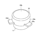
ヨーク24は、プレス加工等で製作できる。ヨーク24の側面部24aに1個以上の外側へ突出したフランジ部が形成されている。図9には、2つのフランジ部24c,24dが示されている。図6,7に示されるように、フランジ部24c等がケース17に設けた溝27a,27b等に嵌合することにより、操作面24bを有するヨーク24がコイル11の軸方向周りに回転することを止めることができる。すなわち、溝27a等は、ヨーク24の回転止めとして機能する。
操作入力装置2は、コイル11の内部に配置され、コア23よりも小径なリターンバネ26を有する。リターンバネ26は、コア23の下面とボビン28の中空部の底部上面に固定され、初期力を伴ってヨーク24をその初期位置に復帰させる。リターンバネ26の下端は、ボビン28の中空部の底部上面に形成された溝状のバネ受け部28aで位置決めされ、リターンバネ26の上端は、コア23の凹部23cに嵌合して位置決めされる。コア23の凹部23cを利用することで、リターンバネ24のバネ長を長くできるため、耐久性向上やバネレート低減等のバネの諸特性を向上させることができる。
図10は、本発明の第3の実施形態である操作入力装置3の斜視断面図である。図11は、操作入力装置3の正面視断面図である。上述の実施形態と同様の構成や効果については、その説明を省略する。
操作入力装置3は、コイル11の外側に設けられたヨーク34の位置が固定されたものである。ヨーク34は、ヨーク材である操作部32の外径よりも内径の大きい円筒部が形成された円筒状部材である。ヨーク34の円筒部の高さは、コイル11の下端11bから操作部32の上端32aまであり、ケース37Aによって固定されている。ヨーク34はケース37とボビン28に囲まれて固定されたまま可動しないので、操作入力により変位する可動部の重量を低減できるので、フィードバック力を付与する時の応答性を向上できる。
マグネット15は、コイル11の内径よりも外径が小さく、操作部32の操作方向と略同一の着磁方向D1に端面着磁されている。コア23は、マグネット15の下面15bに固定され、コイル11の内径よりも小さい。操作部32は、マグネット15の上面15aに固定され、操作入力が作用する上面32aを有する円盤状部材である。ケース37Bは、操作部32の抜け止めである。操作入力装置2は、操作部32に作用する操作入力により、マグネット15とコア23が下方へ同一の変位をする。マグネット15とコア23がコイル11の内側空間をコイル11の軸方向に移動し、操作部32が変位しても、円筒状のヨーク34は可動しない。
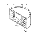
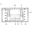
図12は、本発明の第4の実施形態である操作入力装置4の斜視断面図である。図13は、操作入力装置4の正面視断面図である。上述の実施形態と同様の構成や効果については、その説明を省略する。
操作入力装置4は、操作部48の変位により、コア13とヨーク14とマグネット15から構成される磁気回路部分は変位せずに、コイル11が変位するものである。鉄を主成分とするコアやヨークやマグネットを可動部とせずに固定部とすることで、フィードバック力を付与する時の応答性を向上できる。操作部48は、コイル11のボビンとしても機能する。この構成は、例えば本願の他の操作入力装置にも応用できる。
図14は、本発明の第5の実施形態である操作入力装置5の斜視断面図である。図15は、操作入力装置5の正面視断面図である。上述の実施形態と同様の構成や効果については、その説明を省略する。
操作入力装置5は、コイル11の内径よりも小さい外径を有する円筒部が形成された円筒状マグネット55が、磁気回路に磁束を発生させるものである。マグネット55の円筒部は、操作部12の操作方向(コイル11の軸方向)に対して略直角な着磁方向D2に端面着磁されている。コア53は、円柱状に形成され、マグネット55の円筒部の内側に嵌合して固定されている。操作入力装置5は、操作部12に作用する操作入力により、マグネット55とコア53とヨーク14が下方へ同一の変位をする。マグネット55とコア53がコイル11の内側空間をコイル11の軸方向に移動し、円筒状のヨーク14の側面部14aがコイル11の外側空間をコイル11の外側側面に沿って移動する。
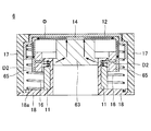
図16は、本発明の第6の実施形態である操作入力装置6の斜視断面図である。図17は、操作入力装置6の正面視断面図である。上述の実施形態と同様の構成や効果については、その説明を省略する。
操作入力装置6は、コイル11の外径よりも大きい内径を有する円筒部が形成された円筒状マグネット65が、磁気回路に磁束を発生させるものである。マグネット65の円筒部は、操作部12の操作方向(コイル11の軸方向)に対して略直角な着磁方向D2に端面着磁されている。円筒状のマグネット65は、カップ状のヨーク14の側面部の内側に嵌合して固定されている。コア63は、円柱状に形成され、ヨーク14の下面に固定され、ボビン18の円筒部の内側にスライド可能に嵌合している。ヨーク14は、コイル11の外径よりも大きく且つ円筒状マグネット65の外径よりも大きい内径を有する円筒状部材である。操作入力装置6は、操作部12に作用する操作入力により、マグネット65とコア63とヨーク14が下方へ同一の変位をする。コア53がコイル11の内側空間をコイル11の軸方向に移動し、マグネット65の円筒部と円筒状のヨーク14の側面部14aがコイル11の外側空間をコイル11の外側側面に沿って移動する。円筒状のマグネット65は、数個に分割されたものでもよい。
次に、コイル11のインダクタンスの変化を検出する検出部と、コイル11に電流を流すことによって、操作部12を可動させる制御部について説明する。
検出部は、コイルのインダクタンスの変化を電気的に検出することで、操作部の連続的に変化するアナログ変位量に応じた検出信号を出力する検出手段である。検出部は、不図示の基板に実装される検出回路によって構成されるとよい。
例えば、検出部は、コイルのインダクタンスの変化に等価的に変化する物理量を検出し、その物理量の検出値を操作部の変位量に等価な値として出力する。また、検出部は、コイルのインダクタンスの変化に等価的に変化する物理量を検出することによりコイルのインダクタンスを算出し、そのインダクタンスの算出値を操作部の変位量に等価な値として出力するものでもよい。また、検出部は、その物理量の検出値又はそのインダクタンスの算出値から操作部の変位量を演算し、その変位量の演算値を出力するものでもよい。
具体的には、検出部は、パルス信号をコイルに供給することによって、コイルのインダクタンスの大きさに対応して変化する信号波形をコイルに発生させ、その信号波形に基づいてコイルのインダクタンスの変化を電気的に検出するとよい。
例えば、コイルの上端面の上方領域における操作部の下方への変位量が増加するにつれて、コイル周辺の透磁率が増加し、コイルのインダクタンスが増加する。コイルのインダクタンスが増加するにつれて、パルス信号の供給によりコイルの両端に発生するパルス電圧波形の振幅も大きくなる。そこで、その振幅をコイルのインダクタンスの変化に等価的に変化する物理量とすることで、検出部は、その振幅を検出することによって、その振幅の検出値を操作部の変位量に等価な値として出力することができる。また、検出部は、その振幅の検出値からコイルのインダクタンスを算出し、そのインダクタンスの算出値を操作部の変位量に等価な値として出力することもできる。
また、コイルのインダクタンスが増加するにつれて、パルス信号の供給によりコイルに流れるパルス電流波形の傾きが緩やかになる。そこで、その傾きをコイルのインダクタンスの変化に等価的に変化する物理量とすることで、検出部は、その傾きを検出することによって、その傾きの検出値を操作部の変位量に等価な値として出力することができる。また、検出部は、その傾きの検出値からコイルのインダクタンスを算出し、そのインダクタンスの算出値を操作部の変位量に等価な値として出力することもできる。
検出部は、例えば、コイルに第1のパルス信号を供給することによってコイルのインダクタンスの変化を検出する検出手段である。検出部は、コイルに第1のパルス信号に対応するパルス電流(第1のパルス電流)を供給することによってコイルの両端に発生するパルス電圧(第1のパルス電圧)に基づいて、コイルのインダクタンスの変化を検出する。コイルのインダクタンスの変化の検出結果に応じて、操作部の変位量を算出することができる。
一方、制御部は、例えば、コイルに第1のパルス信号に対して位相が異なる第2のパルス信号を供給することによって操作部を可動させる磁界を発生させる制御手段である。コイルに第2のパルス信号に対応するパルス電流(第2のパルス電流)が流れることによって生ずる磁界によって、操作部をコアと共にコイルに引き寄せたり引き離したりする力が発生する。コイルに第2のパルス信号が供給されることによって生ずる力の大きさ変動によって、操作部を振動させる。すなわち、第2のパルス信号は、一時的に振幅が変化する信号であるので、操作部に与える力の大きさに変動を与えることができる。
第1のパルス信号及び第2のパルス信号は、矩形波でもよいし、三角波でもよいし、ノコギリ波でもよい。
図18は、インダクタンスの変化を検出する検出部と、操作部を可動させる制御部とを含む制御回路の第1例のブロック図である。制御回路は、コイルLのインダクタンスの変化を検出する算出手段である。制御回路は、CPU等の演算回路70と、演算回路70の第1の出力ポート71に接続された駆動回路76と、演算回路70の第2の出力ポート72とADポート73とに接続された受信回路77とを備える。コイルLは、受信回路77及び駆動回路76を介して、演算回路60に接続される。
駆動回路76は、演算回路70の出力ポート71からの出力信号に応じて定電流源76aの出力電流をコントロールすることによって、コイルLに電流を流す。受信回路77は、コイルLに電流を流すことに伴い発生する電圧を、アンプ77aを通してピークホールド回路77bに入力する(ボトムホールド回路に入力されてもよい)。ピークホールド回路77bによってピークホールドされたピーク値(アナログ値)は、ADポート73に入力されて、ADコンバータによって、デジタル値に変換される。
図19は、図18の各点における波形を示した図である。演算回路70の出力ポート71から矩形波の電圧波形が出力される。この電圧によって、定電流回路76aは、コイルに一定の電流を流す。これにより、コイルは微分波形の電圧V2を発生させる。電圧波形V2として、電圧波形V1の立ち上がりに同期した波形2-1が得られるとともに、電圧波形V1の立下りに同期した波形2-2が得られる。波形2-2は、波形2-1に対して正負が逆側の波形である。アンプ77aは、電圧波形V2を、ADコンバータのダイナミックレンジに適した大きさに増幅する。電圧波形V2をピークホールドするか又はボトムホールドするかによって、そのホールドした値がADコンバータ(ADポート73)に取り込まれる。波形2-1,2-2の振幅値は、各コイルのインダクタンスの大きさに比例して大きくなるため、この振幅値を検出することによって、各コイルのインダクタンスの大きさを評価できる。
図20は、インダクタンスの変化を検出する検出部と、操作部を可動させる制御部とを含む制御回路の第2例のブロック図である。
駆動回路86は、演算回路70の出力ポート71からの出力信号に応じてトランジスタ86aをコントロールすることによって、定電圧出力をコイルLに印加する。操作検出用のコイルLとグランドとの間には抵抗R1が接続され、コイルLと抵抗R1によるローパスフィルタが形成されている。コイルLと抵抗R1の間に発生する電圧V4(抵抗R1の両端電圧)を、アンプ77aを介してピークホールド回路77bに入力する。ピークホールド回路77bによってピークホールドされたピーク値(アナログ値)は、ADポート73に入力されて、ADコンバータによって、デジタル値に変換される。
抵抗R1と並列に接続されているスイッチ素子88は、操作部の変位量を検出するためのパルスを印加する時はオフである。一方、操作部に振動を与えるためのフィードバックパルスを印加する時にコイルLを励起する際、抵抗R1でインピーダンスが高くなり、印加電流が必要分流れないことを回避する必要がある。そのため、スイッチ素子88は、演算回路70の出力ポート74からの出力信号に応じて、フィードバックパルス印加時に同期してオンする。
図21は、図20の各点における波形を示した図である。演算回路70の出力ポート71から矩形波の電圧波形が出力される。この電圧によって、駆動回路86は、コイルLに一定の電圧を印加する。コイルLと抵抗R1との時定数を矩形波パルスの幅以上に設定することにより、図示のような電圧波形V4が発生する。アンプ77aは、このような電圧波形V4を、ADコンバータのダイナミックレンジに適した大きさに増幅する。電圧波形V4をピークホールドすることによって、そのホールドした値がADコンバータ(ADポート73)に取り込まれる。電圧波形V3の振幅値は、コイルLにインダクタンスの大きさに反比例して低くなるため、この振幅値を検出することによって、コイルのインダクタンスの大きさを評価できる。
図22は、インダクタンスの変化を検出する検出部と、操作部を可動させる制御部とを含む制御回路の第3例のブロック図である。
図22に制御回路において、抵抗R1は、コイルLの内部抵抗(抵抗分)に比べて、温度に対する抵抗値の変動誤差が小さいものに設定されている。このように設定された場合、フィードバック力を継続的に出力することによりコイルLの内部抵抗の温度上昇による抵抗値の増加を、矩形波をコイルLに印加したときの電圧波形V4を評価することにより、検知できる。
例えば、コイルLのインダクタンスを操作部が初期位置の場合で0.6mH、最大に押し下げた場合で1.0mHとする。この場合、出力ポート71から出力される矩形波の制御パルスを2μsecの幅に設定し、抵抗R1を470Ωとすると、コイルLと抵抗R1で構成されるフィルターの時定数は1.28μsecである。駆動回路86から出力される印加電圧V5を3Vとし、コイルLの内部抵抗を15Ωに設定すると、操作部の初期位置での電圧波形V3は約2.33Vになり、操作部の最大変位時の電圧波形V3は約1.77Vになる。このように、操作部の変位量に応じて電圧波形V3が変化することから、電圧波形V3を検出することで、操作部の押し込み量を検出できる。
ここで、制御パルスの幅をコイルLと抵抗R1による時定数よりも十分大きい幅にし(又は、制御パルスを直流信号にし)、コイルLに電圧を印加すると、コイルLの内部抵抗と抵抗R1の分圧比に基づいて、電圧波形V3は、2.91V(=3V×470Ω/(470+15)Ω)になる。この2.91Vを、常温23度のときの電圧V3の電圧値とする。
コイルに使用される巻線は一般的に0.4%/℃の温度特性を有している一方、抵抗素子は温度特性を大きく持つものから小さく持つものまで存在し、少ないものでは0.01%/℃程度のものも容易に入手可能である。
そこで、内部抵抗の抵抗値の温度特性が0.4%/℃である素子をコイルLとして使用し、抵抗値の温度特性が0.01%/℃である素子を抵抗R1として使用すると、コイルLの内部温度の加熱上限値100℃のときの電圧V3の電圧値は、常温時の2.91Vに対して2.88Vまで低下する。この温度変化による電圧差30mVを制御回路後段のADコンバータで検出した場合、コイルLへのパルス信号の出力方法を変更又は停止する。これにより、コイルLの内部温度が許容範囲を超える前に、コイルLの破損等を未然に防ぐことができる。
また、インダクタンスの変化を検出するための抵抗R1とは別に、コイルLの内部抵抗を測定するための抵抗R2を、スイッチ素子88とグランドとの間に設けることにより、コイルLの内部抵抗の温度変化を検出する感度を上げてもよい。スイッチ素子88は、フィードバックパルス印加時にインピーダンスを下げて、コイルLに流れる電流値を上げるための素子である。例えば、抵抗値が2Ωであり、その抵抗値の温度特性が0.01%/℃である素子を抵抗R2として使用し、内部抵抗の抵抗値が15Ωであり、その抵抗値の温度特性が0.4%/℃である素子をコイルLとすると、常温25℃のときの電圧V3と高温100℃のときの電圧V3との電圧差は、抵抗R2を設けていない場合の電圧差30mVに対して、74mVに増大させることができるため、その電圧差の検知誤差を抑えることができる。
図23は、操作入力装置を動作させたときの波形図である。
操作入力装置の動作制御方法は、コイルLに第1のパルス信号を供給することによってコイルLのインダクタンスの変化を検出するインダクタンス検出ステップを有する。イン演算回路70は、そのインダクタンス検出ステップで、(b)に示されるように、出力ポート71から、矩形波の電圧波形V1として、コイルLに供給される第1のパルス信号に対応するパルス波形p(p1~p9)を出力する。パルス波形pが出力ポート71から間欠的にコイルLに出力されることによって、第1のパルス信号がコイルLに間欠的に供給される。また、インダクタンス検出ステップが一定の周期で繰り返されることによって、電圧波形V1の各パルス波形p1~p9が一定の周期で出力される。パルス波形pは、コイルLのインダクタンスの変化を検出するための駆動電圧である。
駆動電圧V1によって、(a)に示される操作部の押し下げ量Wに応じて、(c)に示されるように、インダクタンスの増加に伴う検出電圧V3が発生する。押し下げ量Wが(a)に示されるように変化した場合、検出電圧V3の振幅も押し下げ量Wに比例して増加する。押し下げ量Wの増加に伴って検出電圧V3のパルス波形s3,s4,s5の振幅が増加し、押し下げ量Wの減少に伴って検出電圧V3のパルス波形s6,s7の振幅が減少する。押し下げ量Wに変化が無い場合、検出電圧V3のパルス波形の振幅は同一である(s1,s2,s8,s9)。
また、操作入力装置の動作制御方法は、インダクタンス検出ステップで供給される第1のパルス信号に対して位相が異なる第2のパルス信号を、コイルLに供給することによって、操作部をコアやヨークによって可動させる磁界Hを生成する磁界生成ステップを有する。演算回路70は、その磁界生成ステップで、(b)に示されるように、出力ポート71から、矩形波の電圧波形V1として、コイルLに供給される第2のパルス信号に対応するパルス波形q(q1~q5)を出力する。パルス波形qが出力ポート71からコイルLに出力されることによって、第2のパルス信号がコイルLに供給される。パルス波形qが出力されることに伴って、(e)に示されるように、操作部をコイルL側に吸引する力Fが発生する。
図23は、インダクタンスの変化の検出結果である検出電圧V3の振幅に応じて、パルス波形q1~q5を出力する制御方法を示している。すなわち、振幅が所定の閾値未満の検出電圧V3の場合、パルス波形qは出力されず、振幅が所定の閾値以上の検出電圧V3が発生した場合、該検出電圧V3の振幅に対応するパルス波形qが出力される。つまり、押し下げ量Wに応じて操作部の変位を発生させるパルス波形qが、検出電圧V3の振幅に比例した振幅で発生する。そして、パルス波形qの振幅に応じた大きさの吸引力Fが発生する。
インダクタンスの変化を検出するためのパルス波形pの振幅電圧、パルス幅及び出力周期は、インダクタンスの変化を検出電圧V3によって検出できる程度の大きさであればよく、操作者が感知できる操作部の変位を引き起こすことが可能な磁界Hを発生させない程度の大きさであればよい。これにより、インダクタンスの変化を検出するタイミングのたびに、操作者に操作部の変位を感じさせてしまうことを防止することができる。これに対し、パルス波形qに伴い発生する操作部の変位は操作者に確実に感知できるようにするため、パルス波形qの振幅電圧、パルス幅及び周期は、操作者が感知できる操作部の変位を引き起こすことが可能な磁界Hを発生させる程度の大きさであればよい。例えば、パルス波形qの振幅電圧とパルス幅の少なくともいずれか一方は、パルス波形pに比べて、大きくする。
このとき、何ら手当てをしていない場合、操作部に変位を与えるためのパルス波形qが出力されることによって生成された検出電圧V3を、インダクタンスの変化を表す信号として、演算回路70が誤検出することを防ぐため、例えば、(d)に示されるように、パルス波形qが少なくとも発生している期間では、受信回路77を動作させないようにするためのリセット信号VRを発生させてもよい。これにより、パルス波形qが出力されている期間では、(c)に示されるように、検出電圧V3が生成されないようにすることができる。また、パルス波形qは演算回路70が自ら出力するものであるため、パルス波形qに伴い発生する検出電圧V3を、インダクタンスの変化を表す信号として、演算回路70が評価しない(無視する)ようにしてもよい。
また、(b)は、押し下げ量Wの大きさに応じた振幅のパルス波形qが出力される制御方法を示しているが、(f)に示されるように、押し下げ量Wの大きさに応じたパルス幅のパルス波形qを出力して操作部を変位させる制御方法でもよい。押し下げ量Wが大きくなるほど、パルス波形qのパルス幅を広くする。
また、(g)に示されるように、押し下げ量Wの大きさに応じた個数のパルス波形qを出力して操作部を変位させる制御方法でもよい。押し下げ量Wが大きくなるほど、パルス波形qの個数を増大させる。
また、(h)に示されるように、本操作入力装置を使用するアプリケーション(例えば、操作者によって使用される電子機器、より具体的には、ゲーム機器や携帯電話など)によっては、パルス波形qはパルス波形pと必ずしも同期している必要はないため、複数のパルス波形pをまたいで、パルス波形qを発生させる時間間隔(パルス波形qの出力間隔)を変更してもよい。インダクタンスの変化を検出するためのパルス波形pは、インダクタンス変化の検出の時間的分解能(追従速度)に相当するため、短い時間間隔で出力されることが望ましい。一方、操作部に変位を付与するためのパルス波形qは、操作者に操作部の変位が生じたことを感じさせることが必要であるため、パルス波形pに比べて出力間隔を長くする。例えば、(h)に示されるように、パルス波形pに重複しないように、パルス波形pが出力されていない任意の期間に、パルス波形qが出力されればよい。
また、パルス波形pの出力間隔が狭くなり、パルス波形qの出力タイミングを確保することができない場合には、パルス波形qをパルス波形pよりも優先させて、パルス波形qの出力期間ではパルス波形pの出力を停止させてもよい。
また、図23の場合、押し下げ量Wに応じた操作部の変位を発生させているが、パルス波形qの供給態様を変化させることによって、コイルに流れる電流の流れ方が変化するので、操作者に与える振動の態様を変化させることができる。例えば、第2のパルス信号の供給態様を変化させることによりコイルに流す電流の流れ方を変化させることによって、操作者に与える振動の強さ、振動周波数、振動の回数を変化させることができる。また、操作部の変位の発生タイミングを、押し下げ量Wに応じて変化させることに限らず、操作部の押し下げ速度、操作部の操作によって動く対象物(例えば、ディスプレイ上のカーソル、ポインターなど)の移動位置、操作入力装置が使用されるアプリケーション上でのイベント発生に応じて、変化させてもよい。例えば、操作部の押し下げ量Wが所定の値に到達した時に、第2のパルス信号をコイルに供給することによって操作部を変位させる磁界を発生させる。このように操作部に発生させた変位によって、操作者にクリック感を感じさせることができる。
このように、上述の本発明の実施形態の場合、インダクタンスを検出するコイルに印加電圧をフィードバック用に加えるだけで振動を発生できる。例えば、インダクタンスを検出するための検出回路部の駆動回路から出力させる波形の周波数、電圧、間隔などを変化させるだけで、操作部の検出機能と振動の発生機能を実現できる。このように、極めて構成が単純であり、追加するアクチュエータも必要ない。
いわゆる、振動モータのような操作入力装置を含む製品全体(例えば、コントローラー)を振動させるような方法は、製品全体を振動させる強さと時間でしか変化がつけられない。しかしながら、本発明の実施形態であれば、操作部に力の変化を直接出力できる。そのため、例えば複数個の操作入力装置を搭載すれば、その操作部ごとにフィードバックを出力できる(振動させることができる)。また、コントローラーのような製品を持っている手に対してフィードバック振動が伝わることを抑制できるため、直接的な触感を与えることができる。
また、振動モータは振動の振幅を上げるために回転数を上げる必要があり、回転が上がるまでの時間がかかるため応答性が低く、振動周波数と振幅を個別に制御できない。しかしながら、本発明の実施形態であれば、操作部という重量の比較的軽い部位にのみ力を出力するため、出力されるパルスを変更することにより、1パルスでクリック感のような触感を出力することも、パルスを繰り返して振動のような触感を出力することもできる。また、振幅、周波数、パルス幅などを自在に変更できるため、必要に応じて触感を変化させることができる。
以上、本発明の好ましい実施例について詳説したが、本発明は、上述した実施例に制限されることはなく、本発明の範囲を逸脱することなく、上述した実施例に種々の変形、改良及び置換を加えることができる。上述の実施例それぞれの各部の構成を組み合わせてもよい。
例えば、操作部を弾性的に支持する支持部材は、リターンバネのような弾性部材に限らず、ゴム部材でもよいし、スポンジ部材でもよいし、空気や油が充填されたシリンダーでもよい。
また、本発明の操作入力装置は、手指に限らず、手のひらで操作するものあってもよい。また、足指や足の裏で操作するものであってもよい。また、操作者が触れる面は、平面でも、凹面でも、凸面でもよい。
本国際出願は、2011年4月27日に出願した日本国特許出願第2011-100197号に基づく優先権を主張するものであり、日本国特許出願第2011-100197号の全内容を本国際出願に援用する。
本国際出願は、2011年4月27日に出願した日本国特許出願第2011-100197号に基づく優先権を主張するものであり、日本国特許出願第2011-100197号の全内容を本国際出願に援用する。
1~6 操作入力装置
11 コイル
11a 上端
11b 下端
12 操作部(ヨーク)
12a,12b 側面部
12c バネ受け部
13 コア
13a 上面
13b 下面
14 ヨーク
14a 側面部
14b 上面
15 マグネット
15a 上面
15b 下面
16 リターンバネ
17 ケース
17a 溝
18 ボビン
18a バネ受け部
23 コア
23b 下面
23c 凹部
23d バネ受け面
24 ヨーク
24a 側面部
24b 操作面(操作部)
24c,24d フランジ部
26 リターンバネ
27 ケース
27a,27b 溝
28 ボビン
28a バネ受け部
32 ヨーク(操作部)
32a 上端
34 ヨーク
37A,37B ケース
42 ヨーク
47 ケース
48 ボビン(操作部)
53 コア
55 マグネット
63 コア
65 マグネット
70 演算回路
76 駆動回路
77 受信回路
D1,D2 着磁方向
Φ 磁束
S1,S2 領域
11 コイル
11a 上端
11b 下端
12 操作部(ヨーク)
12a,12b 側面部
12c バネ受け部
13 コア
13a 上面
13b 下面
14 ヨーク
14a 側面部
14b 上面
15 マグネット
15a 上面
15b 下面
16 リターンバネ
17 ケース
17a 溝
18 ボビン
18a バネ受け部
23 コア
23b 下面
23c 凹部
23d バネ受け面
24 ヨーク
24a 側面部
24b 操作面(操作部)
24c,24d フランジ部
26 リターンバネ
27 ケース
27a,27b 溝
28 ボビン
28a バネ受け部
32 ヨーク(操作部)
32a 上端
34 ヨーク
37A,37B ケース
42 ヨーク
47 ケース
48 ボビン(操作部)
53 コア
55 マグネット
63 コア
65 マグネット
70 演算回路
76 駆動回路
77 受信回路
D1,D2 着磁方向
Φ 磁束
S1,S2 領域
Claims (26)
- コイルと、
操作入力の作用により前記コイルの軸方向に変位する操作部と、
前記操作部の変位により、前記コイルとの位置関係が変化するコアと、
前記コイルの外側に配置されたヨークと、
前記コアと前記ヨークに流れる磁束を発生させるマグネットとを備え、
前記コイルは、前記操作部の変位量に応じた信号を出力し、
前記操作部は、前記コイルに流れる電流と前記マグネットの磁束によって可動する、操作入力装置。 - 前記コイルが、前記コアと前記ヨークの間に位置する、請求項1に記載の操作入力装置。
- 前記コイルと前記コアと前記ヨークは、前記コアと前記ヨークの間のギャップに発生する磁束が前記軸方向に対して直交するように配置される、請求項2に記載の操作入力装置。
- 前記コイルが、前記操作部が操作されていない非操作状態において、前記コアと前記ヨークに重なっている、請求項1に記載の操作入力装置。
- 前記コアと前記ヨークは、前記操作部が操作されていない非操作状態において、前記軸方向における前記コイルの端面よりも外側に位置する部分を有する、請求項1に記載の操作入力装置。
- 前記ヨークは、前記操作部の変位により、前記コイルとの位置関係が変化する、請求項1に記載の操作入力装置。
- 前記ヨークは、前記コイルの外径よりも大きい内径を有する円筒部が形成された、請求項1に記載の操作入力装置。
- 前記コアは、前記コイルに対向する側の端面に凹部を有する、請求項1に記載の操作入力装置。
- 前記ヨークに形成されたフランジが、前記ヨークを収容する筐体に形成された溝に嵌合する、請求項1に記載の操作入力装置。
- 前記操作部が操作されていない非操作状態の位置に前記操作部を復帰させる付勢部材を備える、請求項1に記載の操作入力装置。
- 前記付勢部材は、前記コイルの内部に配置された、請求項10に記載の操作入力装置。
- 前記付勢部材は、前記コアの前記コイルに対向する側の端面の凹部に嵌合する、請求項11に記載の操作入力装置。
- 前記操作部が、ヨーク材である、請求項1に記載の操作入力装置。
- 前記操作部と前記ヨークが面接触している、請求項13に記載の操作入力装置。
- 前記操作部が、前記操作部を収容する筐体の内面に嵌合する筒部を有する、請求項1に記載の操作入力装置。
- 前記操作部が操作されていない非操作状態の位置に前記操作部を復帰させる付勢部材が、前記操作部の前記筒部に嵌合する、請求項15に記載の操作入力装置。
- 前記ヨークの位置が、固定された、請求項1に記載の操作入力装置。
- 前記マグネットは、前記コイルの内径よりも小さい外径を有する円筒部が形成された、請求項1に記載の操作入力装置。
- 前記コアは、前記マグネットの前記円筒部に嵌合する、請求項18に記載の操作入力装置。
- 前記マグネットは、前記コイルの外径よりも大きい内径を有する円筒部が形成された、請求項1に記載の操作入力装置。
- 前記ヨークは、前記コイルの外径よりも大きく且つ前記マグネットの前記円筒部の外径よりも大きい内径を有する円筒部が形成された、請求項20に記載の操作入力装置。
- 前記操作部の変位により、前記コイルが変位する、請求項1に記載の操作入力装置。
- 前記コアの位置が、固定された、請求項22に記載の操作入力装置。
- 前記マグネットの位置が、固定された、請求項23に記載の操作入力装置。
- コイルと、
操作入力の作用により前記コイルの軸方向に変位する操作部と、
前記操作部の変位により、前記コイルとの位置関係が変化するコア及びヨークと、
前記コアと前記ヨークとの間に配置されたマグネットとを有し、
前記コイルは、前記操作部の変位量に応じた信号を出力し、
前記操作部は、前記コイルに流れる電流と前記マグネットの磁束によって可動する、操作入力装置。 - 請求項1に記載の操作入力装置と、
前記コイルのインダクタンスの変化を検出する検出手段と、
前記コイルに電流を流すことによって、前記操作部を可動させる制御手段とを備える、操作入力検出装置。
Priority Applications (2)
| Application Number | Priority Date | Filing Date | Title |
|---|---|---|---|
| CN201280020373.4A CN103492830B (zh) | 2011-04-27 | 2012-04-26 | 操作输入装置以及操作输入检测装置 |
| US14/113,246 US9075440B2 (en) | 2011-04-27 | 2012-04-26 | Operation input device and operation input detecting device |
Applications Claiming Priority (2)
| Application Number | Priority Date | Filing Date | Title |
|---|---|---|---|
| JP2011-100197 | 2011-04-27 | ||
| JP2011100197A JP5842376B2 (ja) | 2011-04-27 | 2011-04-27 | 操作入力装置及び操作入力検出装置 |
Publications (1)
| Publication Number | Publication Date |
|---|---|
| WO2012147866A1 true WO2012147866A1 (ja) | 2012-11-01 |
Family
ID=47072381
Family Applications (1)
| Application Number | Title | Priority Date | Filing Date |
|---|---|---|---|
| PCT/JP2012/061249 Ceased WO2012147866A1 (ja) | 2011-04-27 | 2012-04-26 | 操作入力装置及び操作入力検出装置 |
Country Status (4)
| Country | Link |
|---|---|
| US (1) | US9075440B2 (ja) |
| JP (1) | JP5842376B2 (ja) |
| CN (1) | CN103492830B (ja) |
| WO (1) | WO2012147866A1 (ja) |
Families Citing this family (14)
| Publication number | Priority date | Publication date | Assignee | Title |
|---|---|---|---|---|
| JP6190751B2 (ja) * | 2014-04-11 | 2017-08-30 | 株式会社Soken | タッチパネル式入力装置 |
| JP6278355B2 (ja) * | 2014-08-08 | 2018-02-14 | アルプス電気株式会社 | 振動発生装置及び入力装置 |
| DE102014226976A1 (de) * | 2014-12-23 | 2016-06-23 | Continental Automotive Gmbh | Eingabevorrichtung, aufweisend eine Vorrichtung zur Erzeugung haptischer Rückmeldungen |
| JP6418642B2 (ja) * | 2015-01-22 | 2018-11-07 | アルプス電気株式会社 | 入力装置 |
| JP6464927B2 (ja) * | 2015-03-03 | 2019-02-06 | 株式会社Soken | 入力装置 |
| US11295935B2 (en) * | 2015-05-11 | 2022-04-05 | Ebara Corporation | Electromagnet device, electromagnet controller, electromagnet control method, and electromagnet system |
| EP3321775A4 (en) * | 2015-07-08 | 2018-07-04 | Alps Electric Co., Ltd. | Tactile sensation reproduction device |
| CN107957231B (zh) * | 2017-12-28 | 2024-02-02 | 湖南北斗微芯产业发展有限公司 | 一种地质类磁传动位移检测器及检测方法 |
| US20210173491A1 (en) * | 2018-02-08 | 2021-06-10 | Hewlett-Packard Development Company, L.P. | Keyboard keys |
| US11450462B2 (en) | 2019-02-18 | 2022-09-20 | Canon Kabushiki Kaisha | Operation device that produces clicking sensation, and electronic apparatus |
| CN112881206B (zh) * | 2021-01-14 | 2025-02-14 | 西北工业大学 | 一种产生大位移的电磁加载装置及其试验方法 |
| FI20215680A1 (en) | 2021-06-10 | 2021-06-10 | Ps Audio Design Oy | SURFACE AUDIO DEVICE WITH HAPTIC OR AUDIO FEEDBACK |
| CN113871240B (zh) * | 2021-09-30 | 2024-04-30 | 歌尔股份有限公司 | 扳机按键装置和电子设备 |
| CN114470739B (zh) * | 2021-12-31 | 2024-10-18 | 歌尔股份有限公司 | 一种按键结构和游戏机 |
Citations (7)
| Publication number | Priority date | Publication date | Assignee | Title |
|---|---|---|---|---|
| JPH04362722A (ja) * | 1991-06-10 | 1992-12-15 | Fujitsu Ltd | 抗力可変装置、及びキースイッチ装置 |
| JPH09222301A (ja) * | 1996-02-19 | 1997-08-26 | Zexel Corp | 位置検出方法及び磁気飽和型位置検出装置 |
| JPH09231008A (ja) * | 1996-02-20 | 1997-09-05 | Fujitsu Takamizawa Component Kk | 小型コンピュータおよびポインティングデバイス |
| JPH1055251A (ja) * | 1996-08-09 | 1998-02-24 | N T T Data Tsushin Kk | マウス |
| JP2003173725A (ja) * | 2001-12-05 | 2003-06-20 | Parusumo Kk | 照光型押しボタンスイッチ、発光機構及び発光制御プログラム |
| JP2007129678A (ja) * | 2005-10-06 | 2007-05-24 | Sony Corp | アクチュエータおよびタッチパネルディスプレイ装置並びに電子機器 |
| JP2009123245A (ja) * | 2009-03-10 | 2009-06-04 | Fujitsu Component Ltd | 入力装置および電子機器 |
Family Cites Families (7)
| Publication number | Priority date | Publication date | Assignee | Title |
|---|---|---|---|---|
| JPH01199101A (ja) * | 1988-02-04 | 1989-08-10 | Kougakushiya:Kk | 位置検出機能を有する電磁アクチュエータ |
| JPH0313802A (ja) * | 1989-06-13 | 1991-01-22 | Furukawa Electric Co Ltd:The | ソレノイドの鉄芯位置判別方法 |
| CN2086311U (zh) * | 1991-02-28 | 1991-10-09 | 浙江省玉环县西台红旗机械一厂 | 电磁开关 |
| US6816049B2 (en) * | 2002-09-19 | 2004-11-09 | Fuji Xerox Co., Ltd. | Actuator |
| US7336006B2 (en) * | 2002-09-19 | 2008-02-26 | Fuji Xerox Co., Ltd. | Magnetic actuator with reduced magnetic flux leakage and haptic sense presenting device |
| JP2005275632A (ja) | 2004-03-23 | 2005-10-06 | Fujitsu Component Ltd | 入力パネル及び入力装置 |
| JP2007087274A (ja) * | 2005-09-26 | 2007-04-05 | Jr Higashi Nippon Consultants Kk | 触覚装置及び触覚情報伝達システム |
-
2011
- 2011-04-27 JP JP2011100197A patent/JP5842376B2/ja active Active
-
2012
- 2012-04-26 CN CN201280020373.4A patent/CN103492830B/zh not_active Expired - Fee Related
- 2012-04-26 WO PCT/JP2012/061249 patent/WO2012147866A1/ja not_active Ceased
- 2012-04-26 US US14/113,246 patent/US9075440B2/en not_active Expired - Fee Related
Patent Citations (7)
| Publication number | Priority date | Publication date | Assignee | Title |
|---|---|---|---|---|
| JPH04362722A (ja) * | 1991-06-10 | 1992-12-15 | Fujitsu Ltd | 抗力可変装置、及びキースイッチ装置 |
| JPH09222301A (ja) * | 1996-02-19 | 1997-08-26 | Zexel Corp | 位置検出方法及び磁気飽和型位置検出装置 |
| JPH09231008A (ja) * | 1996-02-20 | 1997-09-05 | Fujitsu Takamizawa Component Kk | 小型コンピュータおよびポインティングデバイス |
| JPH1055251A (ja) * | 1996-08-09 | 1998-02-24 | N T T Data Tsushin Kk | マウス |
| JP2003173725A (ja) * | 2001-12-05 | 2003-06-20 | Parusumo Kk | 照光型押しボタンスイッチ、発光機構及び発光制御プログラム |
| JP2007129678A (ja) * | 2005-10-06 | 2007-05-24 | Sony Corp | アクチュエータおよびタッチパネルディスプレイ装置並びに電子機器 |
| JP2009123245A (ja) * | 2009-03-10 | 2009-06-04 | Fujitsu Component Ltd | 入力装置および電子機器 |
Also Published As
| Publication number | Publication date |
|---|---|
| CN103492830B (zh) | 2016-08-31 |
| US9075440B2 (en) | 2015-07-07 |
| US20140049514A1 (en) | 2014-02-20 |
| JP2012230086A (ja) | 2012-11-22 |
| CN103492830A (zh) | 2014-01-01 |
| JP5842376B2 (ja) | 2016-01-13 |
Similar Documents
| Publication | Publication Date | Title |
|---|---|---|
| JP5842376B2 (ja) | 操作入力装置及び操作入力検出装置 | |
| JP5782917B2 (ja) | 操作入力装置 | |
| US10586431B2 (en) | Haptic system with increased LRA bandwidth | |
| JP4213539B2 (ja) | 座標入力装置 | |
| JP7371895B2 (ja) | アクチュエーター | |
| US10845883B2 (en) | Method for generating a haptic effect and device employing the method | |
| JP2011090963A (ja) | 操作入力装置及びその制御方法 | |
| JP2021081876A (ja) | 振動アクチュエータ及び振動呈示装置 | |
| JP7605554B2 (ja) | 振動アクチュエータ及び振動提示装置 | |
| KR101324201B1 (ko) | 진동발생 모듈, 이를 이용한 액추에이터, 및 휴대용 기기 | |
| JP5120422B2 (ja) | 操作入力装置 | |
| US20170153722A1 (en) | Capacitive stylus and operation system for the same | |
| JP2014146208A (ja) | 振動発生装置及びタッチパネル装置 | |
| KR101224432B1 (ko) | 진동발생 모듈, 이를 이용한 액추에이터, 및 휴대용 기기 | |
| KR101286471B1 (ko) | 진동발생 모듈, 이를 이용한 액추에이터, 및 휴대용 기기 | |
| KR20110036142A (ko) | 전자기유도현상을 이용한 외력 반응형 햅틱제공장치, 이를 이용한 햅틱제공모듈, 이를 이용한 휴대단말기 및 그 제어방법 | |
| TW202435551A (zh) | 控制裝置以及振動呈現裝置 | |
| KR102360110B1 (ko) | 포스 센서를 포함하는 진동 발생 장치 | |
| JP2013065495A (ja) | 入力検知装置 | |
| EP4343496B1 (en) | Control device and vibration presenting apparatus | |
| JP5751142B2 (ja) | 操作検出回路、操作検出装置、操作検出制御装置及び電子機器 | |
| KR101067639B1 (ko) | 방향전환수단을 구비한 강성구현장치, 이를 이용한 햅틱장치, 이를 이용한 초소형 이동체 및 그 제어방법 |
Legal Events
| Date | Code | Title | Description |
|---|---|---|---|
| 121 | Ep: the epo has been informed by wipo that ep was designated in this application |
Ref document number: 12777505 Country of ref document: EP Kind code of ref document: A1 |
|
| WWE | Wipo information: entry into national phase |
Ref document number: 14113246 Country of ref document: US |
|
| NENP | Non-entry into the national phase |
Ref country code: DE |
|
| 122 | Ep: pct application non-entry in european phase |
Ref document number: 12777505 Country of ref document: EP Kind code of ref document: A1 |