WO2012147753A1 - 中継衛星および衛星通信システム - Google Patents
中継衛星および衛星通信システム Download PDFInfo
- Publication number
- WO2012147753A1 WO2012147753A1 PCT/JP2012/060995 JP2012060995W WO2012147753A1 WO 2012147753 A1 WO2012147753 A1 WO 2012147753A1 JP 2012060995 W JP2012060995 W JP 2012060995W WO 2012147753 A1 WO2012147753 A1 WO 2012147753A1
- Authority
- WO
- WIPO (PCT)
- Prior art keywords
- signal
- reception
- transmission
- delay
- unit
- Prior art date
Links
Images


Classifications
-
- H—ELECTRICITY
- H04—ELECTRIC COMMUNICATION TECHNIQUE
- H04B—TRANSMISSION
- H04B7/00—Radio transmission systems, i.e. using radiation field
- H04B7/14—Relay systems
- H04B7/15—Active relay systems
- H04B7/185—Space-based or airborne stations; Stations for satellite systems
- H04B7/18578—Satellite systems for providing broadband data service to individual earth stations
-
- H—ELECTRICITY
- H04—ELECTRIC COMMUNICATION TECHNIQUE
- H04B—TRANSMISSION
- H04B7/00—Radio transmission systems, i.e. using radiation field
- H04B7/14—Relay systems
- H04B7/15—Active relay systems
- H04B7/185—Space-based or airborne stations; Stations for satellite systems
- H04B7/1851—Systems using a satellite or space-based relay
- H04B7/18515—Transmission equipment in satellites or space-based relays
-
- H—ELECTRICITY
- H04—ELECTRIC COMMUNICATION TECHNIQUE
- H04B—TRANSMISSION
- H04B7/00—Radio transmission systems, i.e. using radiation field
- H04B7/14—Relay systems
- H04B7/15—Active relay systems
- H04B7/204—Multiple access
- H04B7/2041—Spot beam multiple access
Definitions
- the present invention relates to a relay satellite that relays various signals from a narrowband signal to an ultra-wideband signal, and a satellite communication system using the relay satellite.
- each sampling rate of the AD converter (A / D), DA converter (D / A), and digital signal processing unit is set.
- a technique related to such a relay satellite equipped with a digital channelizer is disclosed in Patent Document 1 below.
- space devices with excellent radiation resistance generally have a lower sampling rate and processing speed than consumer devices used on the ground. There was a problem that it could not be realized due to device performance limitations.
- the present invention has been made in view of the above, and an object of the present invention is to obtain a relay satellite and a satellite communication system that can relay a signal having a wider band than before and that are resistant to failure and interference.
- a relay satellite includes a plurality of reception antennas, a plurality of reception processing means, a plurality of transmission processing means, a plurality of transmission antennas, First switching means for outputting a signal received by each of the receiving antennas to one or more of the reception processing means, and a digital reception signal obtained by performing reception processing by each of the plurality of reception processing means.
- Second switch means for outputting to one or more of the transmission processing means, and a second switch means for outputting an analog signal obtained by each of the plurality of transmission processing means to one of the transmission antennas.
- the first switch means receives the wideband received signal when a received signal having a wider band than the band that can be processed by the reception processing means is input.
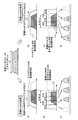
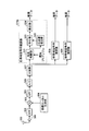
- FIG. 1 is a diagram showing a configuration of a relay satellite according to the present invention.
- FIG. 2 is a diagram illustrating an internal configuration example of components that perform processing on the reception side in the relay satellite.
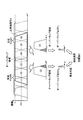
- FIG. 3 is a diagram illustrating an internal configuration example of components that perform transmission-side processing in the relay satellite.
- FIG. 4 is a diagram illustrating a configuration example of a receiving station.
- FIG. 5 is a diagram illustrating a configuration example of a combining unit included in the receiving station.
- FIG. 6 is a diagram showing an outline of a signal relay operation example.
- FIG. 7 is a diagram illustrating an example of the signal relay operation (reception side).
- FIG. 1 is a diagram showing a configuration of a relay satellite according to the present invention.
- FIG. 2 is a diagram illustrating an internal configuration example of components that perform processing on the reception side in the relay satellite.
- FIG. 3 is a diagram illustrating an internal configuration example of components that perform transmission-side processing in the relay satellite.
- FIG. 8 is a diagram illustrating a relationship between spectrums of signals processed by the demultiplexing unit of the reception port #n and the demultiplexing unit of the reception port # n + 1.
- FIG. 9 is a diagram illustrating an example of a signal received by the reception port # 2.
- FIG. 10 is a diagram illustrating an example of the signal relay operation (transmission side).
- FIG. 11 is a diagram illustrating an example of a wideband signal transmitted from the relay satellite to the receiving station.
- FIG. 12 is a diagram illustrating an example of delay processing in the signal relay operation.
- FIG. 13 is a diagram illustrating an example of cross-correlation characteristics.
- FIG. 14 is a diagram illustrating an example of a signal vector synthesized at the receiving station.
- FIG. 15 is a diagram illustrating a frame format of a signal processed by the relay satellite according to the second embodiment.
- FIG. 16 is a diagram illustrating a configuration example of a receiving station that receives a signal relayed by the relay satellite according to the second embodiment.
- FIG. 17 is a diagram illustrating a configuration example of a digital switch matrix unit according to the fourth embodiment.
- FIG. 18 is a diagram illustrating an example of processing of the phase compensation unit included in the digital switch matrix unit.
- FIG. 19 is a diagram illustrating an example of the relationship between the same components of reception signals input to two different reception ports.
- FIG. 20 is a diagram illustrating an example of the relationship between the same components of reception signals input to two different reception ports.
- FIG. 21 is a diagram illustrating an operation example of the path delay difference detection unit provided in the digital switch matrix unit.
- FIG. 22 is a diagram illustrating a configuration example of a digital switch matrix unit according to the fourth embodiment.
- FIG. 23 is a diagram illustrating an example of a wideband signal transmitted from the relay satellite to the receiving station.
- FIG. 24 is a diagram illustrating an example of a relationship between signals output from two different transmission ports and transmitted from the same transmission antenna.
- FIG. 25 is a diagram illustrating an example of cross-correlation characteristics.
- FIG. 26 is a diagram showing details of the cross-correlation characteristics shown in FIG.
- FIG. 27 is a diagram illustrating an internal configuration example of a receiving unit that performs processing on the receiving side in the relay satellite according to the sixth embodiment.
- FIG. 28 is a diagram illustrating an internal configuration example of a transmission unit that performs processing on the transmission side in the relay satellite according to the sixth embodiment.
- Embodiment 1 FIG.
- a relay satellite and a satellite communication system capable of relaying a wideband signal using a device having a low sampling rate and a processing rate will be described.
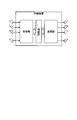
- the relay satellite relays four uplink signal meters ( ⁇ A, B, C, D ⁇ ) from two beam areas to the two beam areas. This is also applicable to the case where is 3 or more, or the case where there are 5 or more signals to be relayed.
- FIG. 1 is a diagram illustrating a configuration example of a relay satellite according to the present invention.
- the relay satellite includes a receiving unit that receives a signal, a transmitting unit that transmits the signal, and a connection that passes the signal received by the receiving unit to the transmitting unit. , A plurality of receiving antennas connected to the receiving unit, and a plurality of transmitting antennas connected to the transmitting unit, performing signal processing to be described later on a signal received via the receiving antenna, Relay signals by transmitting.
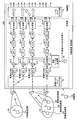
- FIG. 2 is a diagram showing an example of the internal configuration of a component that performs processing on the receiving side in the relay satellite shown in FIG. 1, specifically, a receiving unit and a connecting unit.
- a signal transmission source device transmission station
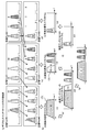
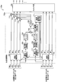
- the relay satellite 200 is a receiving antenna 21-1, 21-2,... That receives signals from the wideband beam area 100, the narrowband beam area 102, as a component that performs processing on the reception side.
- 21-N reception analog switch matrix unit 22, bandpass filters 23-1, 23-2, 23-3,..., 23-N, mixers 24-1, 24-2, 24-3,.
- 24-N reception local generation unit 25, original oscillation 26, low pass filters (LPF) 27-1, 27-2, 27-3,..., 27-N, and AD converter (A / D) 28 , 28-N, delay circuits 29-1, 29-2, 29-3,..., 29-N, demultiplexing units 30-1, 30-2, 30-3,..., 30-N, and the digital switch matrix unit 31 Equipped with a.
- the reception analog switch matrix unit to the demultiplexing unit constitute the reception unit shown in FIG.
- the digital switch matrix part constitutes the connection part shown in FIG.
- a broadband transmission station 101 exists in the broadband beam area 100, and narrowband transmission stations 103, 104, and 105 exist in the narrowband beam area 102.
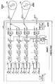
- FIG. 3 is a diagram illustrating an example of an internal configuration of a component that performs processing on the transmission side in the relay satellite illustrated in FIG. 1, specifically, a transmission unit.
- a transmission destination device receiving station
- the relay satellite 200 includes, as components for performing processing on the transmission side, multiplexing units 32-1, 32-2, 32-3,..., 32-N, and a delay circuit 33-1. , 33-2, 33-3, ..., 33-N, DA converters (D / A) 34-1, 34-2, 34-3, ..., 34-N, and a low-pass filter (LPF) 35- 1, 35-2, 35-3,..., 35-N, mixers 36-1, 36-2, 36-3,..., 36-N, a transmission local generator 37, and a band pass filter (BPF).
- D / A DA converters
- LPF low-pass filter
- a receiving station 401 exists in the beam area 400 and a receiving station 403 exists in the beam area 402.
- FIG. 4 is a diagram showing a configuration example of the receiving station 401 in the present embodiment, and the receiving station 401 is a spread spectrum receiving station. That is, in this embodiment, a relay satellite that relays signals to a spread spectrum receiving station will be described.
- the receiving station 401 of this embodiment includes an antenna 500, an amplifier 501, a band pass filter (BPF) 502, a mixer 503, a reception local generation unit 504, a low pass filter (LPF). ) 505, an AD converter (A / D) 506, a demultiplexing unit 507, a wideband signal demodulator 510, and narrowband signal demodulators 508 and 509.
- the broadband signal demodulator 510 includes a cross correlator 511, a vector phase detector 512, a combiner 513, and a detector 514.
- FIG. 5 is a diagram illustrating a configuration example of the combining unit 513 provided in the receiving station 401.
- the synthesizer 513 includes delay units 600 and 601 that process delay amounts and cross-correlation data, and a transfer unit 610 and a phase shifter for data processed by the delay units 600 and 601. 611, an adder 620, and a latch 630.
- FIG. 6 is a diagram illustrating an example of a signal relay operation by the relay satellite according to the present embodiment.
- relay satellite 200 simultaneously relays the following signals A, B, C, and D in the frequency arrangement shown in FIG. ⁇ 1>
- a wideband signal A from the wideband transmitting station 101 in the wideband beam area 100 is transmitted to the receiving station 401 in the beam area 400.
- B is transmitted to the receiving station 403 in the beam area 402
- the narrowband signal C from the narrowband transmitting station 104 in the narrowband beam area 102 is transmitted to the receiving station 401 in the beam area 400
- narrow Narrowband signal D from narrowband transmitting station 105 in band beam area 102 is transmitted to receiving station 401 in beam area 400.
- the upper limit of the signal bandwidth that can be processed by a set of ⁇ AD converter, demultiplexing unit, multiplexing unit, DA converter ⁇ in the relay satellite 200 is set to 1, and the bandwidth of the wideband signal A is Assuming a case where the width is 1.5 and the bandwidths of the narrowband signals B, C, and D are 0.25, the prior art cannot digitally demultiplex, multiplex, or switch the wideband signal A. .
- the present embodiment details will be described later, but each signal ⁇ A, B, C, D ⁇ including such a broadband signal A is relayed while preventing deterioration in communication quality. .
- the broadband signal A is received by the reception antenna 21-1 and input to the reception analog switch matrix unit 22.
- the narrowband signals B, C, and D are received by the receiving antenna 21-2 and similarly input to the receiving analog switch matrix unit 22.
- the reception analog switch matrix unit 22 is controlled by a command signal from the ground control station 110.
- the command signal is transmitted from the control station 110 to the relay satellite 200 via a separate line.
- the reception analog switch matrix unit 22 follows the command signal from the control station 110, and for the wideband signal A from the reception antenna 21-1, the bandpass filter (BPF) 23 corresponding to the subsequent reception port # 0. ⁇ 1 and the band pass filter (BPF) 23-2 corresponding to the reception port # 1 at the subsequent stage are simultaneously input.
- the wideband signal A input to the BPF 23-1 is frequency-converted from a radio frequency band to an intermediate frequency band or a baseband band via a mixer 24-1 and a low-pass filter (LPF) 27-1 at the subsequent stage.
- the analog signal (pass bandwidth 1.0) of the BPF 23-1 and the LPF 27-1 causes the wideband signal A to be cut in almost half of the lower band from the center frequency as shown in FIG. And its bandwidth is reduced from 1.5 to 0.75 + ⁇ .
- the wideband signal A input to the BPF 23-2 is frequency-converted from the radio frequency band to the intermediate frequency band or the baseband band via the mixer 24-2 and the low pass filter (LPF) 27-2 in the subsequent stage. Is done.
- the analog signal (pass bandwidth 1.0) by the BPF 23-2 and the LPF 27-2 is used to reduce the band half of the wide band signal A from the center frequency. And its bandwidth is reduced from 1.5 to 0.75 + ⁇ .
- the bandwidth may not be half, and the signal bandwidth input to the AD converters 28-1 and 28-2 at the subsequent stage is not limited. Any ratio (for example, 0.9 + ⁇ : 0.6 + ⁇ ) may be used as long as it is 1 or less (below the upper limit of the processing speed).
- the relationship of this ratio is that the frequency of the local signal input from the reception local generation unit 25 to the mixer 24-1 and the frequency of the local signal input from the reception local generation unit 25 to the mixer 24-2 This is realized by controlling with a command signal from 110. Since each local signal generated from the reception local generation unit 25 is generated based on the original oscillation 26, the frequency relationship of each local signal is stable and no frequency shift occurs.
- the frequency interval of these reception local signals is 1. That is, by setting the frequency interval of the received local signal to the same value as the upper limit value 1 of the signal bandwidth that can be processed by each ⁇ AD converter, demultiplexing unit, multiplexing unit, DA converter ⁇ , the relay satellite 200 Realizes relay processing of a wideband signal having the maximum bandwidth N with the configuration of the reception ports # 0 to # N-1 shown in FIG.
- the signal in FIG. 7A sampled by the AD converter 28-1 is subjected to a time delay of ⁇ R0 [seconds] by the delay circuit 29-1, and is then demultiplexed including an out-of-band signal.
- the signal is decomposed into four signals by the unit 30-1.
- the signal input to the AD converter 28-1 is an intermediate frequency (IF) signal
- the AD converter 28-1 samples the IF signal.
- the signal input to the AD converter 28-1 is a baseband signal
- the AD converter 28-1 samples the baseband signal with two types of in-phase (I) and quadrature (Q).
- the number of demultiplexing is four, but the number of demultiplexing is not limited to this, and any value may be used as long as it is an integer of 2 or more.
- the characteristics of the four filters (demultiplexing filters) used in the demultiplexing unit 30-1 are indicated by dotted lines in FIG. With this processing, the demultiplexing unit 30-1 deletes ⁇ from the signal having the bandwidth 0.75 + ⁇ shown in FIG. 7A, and the signal (A) having the bandwidth 0.75 shown in FIG. As shown in FIG. 7C, the signal is decomposed into three signals (1), (2), and (3) having a bandwidth of 0.25. As shown in FIG. 7C, the demultiplexing unit 30-1 demultiplexes signals including out-of-band signals.
- the signal (bandwidth 0.75 + ⁇ ) of FIG. 7D sampled by the AD converter 28-2 is demultiplexed after being given a time delay of ⁇ R1 [seconds] by the delay circuit 29-2.
- the signals including the out-of-band signals are decomposed into four signals as shown in FIG. 7 (f) by the four demultiplexing filters having the characteristics shown by the dotted lines in FIG. 7 (e). That is, the demultiplexing unit 30-2 deletes ⁇ from the signal having the bandwidth 0.75 + ⁇ shown in FIG. 7D, and the signal (A) having the bandwidth 0.75 shown in FIG. As shown in FIG. 7F, the signal is decomposed into three signals (4), (5), and (6) having a bandwidth of 0.25.
- Fig. 8 shows the relationship between the frequency vs. amplitude characteristics of the demultiplexer corresponding to each port.
- the four frequency versus amplitude characteristics indicated by the solid line are the characteristics of the four filters provided in the demultiplexing unit corresponding to the reception port #n
- the four frequency versus amplitude characteristics indicated by the dotted line are The characteristics of the four filters provided in the demultiplexing unit corresponding to the reception port # n + 1.
- the characteristics of the filters used in each demultiplexing unit are designed such that the characteristics overlap between adjacent filters, including between reception port #n and reception port # n + 1.
- the amplitude at which the characteristics of each filter intersect is 0.5, and the sum of the frequency-amplitude characteristics of each filter is 1.
- each filter shown in FIG. 8A is designed to be a straight line without any discontinuity, for example, the input signal A once becomes signals (1), (2), (3), Even if it is decomposed into six (4), (5), and (6) (see FIGS. 7 (c) and (f)), by the multiplexing process by the multiplexing units 32-1 to 32-N in the subsequent stage, The signals (a) and (a) are restored (FIG. 8B), and the original signal A is restored by signal synthesis processing in the transmission analog switch matrix unit 39 (FIG. 8C).
- the design in which the frequency vs. phase characteristic of each filter shown in FIG. 8A is a straight line within the reception port (reception port #n, reception port # n + 1) is the demultiplexing unit 30-1 to 30-N. Is possible because it is composed of digital circuits.
- the frequency vs. phase characteristic of each filter including a straight line including between the reception port #n and the reception port # n + 1 is different from the characteristics of the analog filter at each reception port, and the phase noise of each reception local signal Difficult because of its characteristics. This countermeasure will be described later.
- the reception analog switch matrix unit 22 applies the signal ⁇ B, C, D ⁇ from the reception antenna 21-2 to the bandpass filter (BPF) corresponding to the reception port # 2 according to the command signal from the control station 110. ) Input to 23-3.
- the narrowband signal ⁇ B, C, D ⁇ input to the BPF 23-3 passes from the radio frequency band to the intermediate frequency band or the baseband band via the mixer 24-3 and the low-pass filter (LPF) 27-3. Frequency conversion is performed.
- the analog filter by the BPF 23-3 and the LPF 27-3 extracts the signal ⁇ B, C, D ⁇ , and removes the unnecessary wave when the unnecessary wave exists in the adjacent frequency band (FIG. 9A). FIG. 9 (b)).
- the signal ⁇ B, C, D ⁇ of FIG. 9B sampled by the AD converter 28-3 is given a time delay of ⁇ R2 [seconds] by the delay circuit 29-3, and then the demultiplexing unit 30- 3, the four filter characteristics indicated by the dotted lines in FIG. 9C are decomposed into four signals as shown in FIG. 9D, including signals outside the band.
- the demultiplexing unit 30-3 decomposes (demultiplexes) the signals ⁇ B, C, D ⁇ shown in FIG. 9C into three narrowband signals B, C, D.
- the digital switch matrix unit 31 receives the signals output from the preceding demultiplexing units, and distributes the input signals to the subsequent combining units 32-1 to 32-N.
- the signals B, C, and D output from the demultiplexing unit 30-3 are input, and the switch process shown in FIG. 10A is performed.
- the signal (1) is the terminal # 0 0 , that is, the 0th terminal among the m terminals corresponding to the transmission port # 0, and the signal (2) is the terminal # 0 1 ( Signal (3) is at terminal # 0 2 (second terminal corresponding to transmission port # 0) and signal (4) is at terminal # 0 3 (transmission port # 0).
- Signal (5) corresponds to terminal # 1 0 (0th terminal corresponding to transmission port # 1)
- signal (6) corresponds to terminal # 1 1 (3rd terminal corresponding to transmission port # 1).
- Each multiplexing unit (multiplexing units 32-1 to 32-N) synthesizes four input signals by arranging them at a frequency interval of 0.25.
- each multiplexing unit has a circuit design in which the frequency-to-phase characteristic of the combined signal is a straight line like the demultiplexing units 30-1 to 30-N.
- the multiplexing unit 32-1 combines the signals (1), (2), (3), and (4) input from the digital switch matrix unit 31, and the result is shown in FIG.
- the signal (C) shown is generated.
- the multiplexing unit 32-2 multiplexes the signals (5), (6), C, and D to generate signals ⁇ (d), C, D ⁇ having the frequency arrangement shown in FIG.
- the multiplexing unit 32-3 generates the signal B having the frequency arrangement shown in FIG. 10D by the process of multiplexing the signal B and three empty channels.
- the combined signal (c) is converted into a radio frequency band via the delay circuit 33-1, the DA converter 34-1, the LPF 35-1, the mixer 36-1, and the BPF 38-1.
- the combined signals ⁇ (D), C, D ⁇ are transmitted wirelessly via the delay circuit 33-2, DA converter 34-2, LPF 35-2, mixer 36-2, and BPF 38-2.
- the signal B after being converted into the frequency band and combined is converted into the radio frequency band via the delay circuit 33-3, the DA converter 34-3, the LPF 35-3, the mixer 36-3, and the BPF 38-3.
- the number of multiplexing is four is shown.
- the number of multiplexing is not limited to this, and any value can be used as long as it is an integer of 2 or more. It doesn't matter.
- the delay amounts ⁇ T0, ⁇ T1, ⁇ T2,..., ⁇ T (n ⁇ 1) of the delay circuits 33-1, 33-2, 33-3,..., 33-N are determined by command signals from the ground control station 110. Be controlled. The setting of each delay amount will be described later.
- Each transmission signal is converted into a radio frequency band by multiplying each transmission local signal generated by the transmission local generation unit 37 by each mixer 36-1, 36-2, 36-3, ..., 36-N. Realized.
- Each transmission local signal generated by the transmission local generation unit 37 is generated on the basis of the original oscillation 26 in the same manner as each reception local signal generated by the reception local generation unit 25 described above. Therefore, the frequency relationship of each transmission local signal is stable and no frequency shift occurs. Also, the frequency interval of these transmission local signals is set to 1 similarly to the frequency interval of the reception local signals.
- the connection of the transmission analog switch matrix unit 39 is controlled by a command signal from the control station 110 on the ground.
- the signal (c) from the transmission port # 0 (BPF 38-1) and the signal ⁇ (d), C, D ⁇ from the transmission port # 1 (BPF 38-2) are simultaneously transmitted to the transmission antenna 40- Output to 1.
- the signal spectrum output from the transmission antenna 40-1 has a form in which the signal (c) and the signal (d) partially overlap.
- the frequency interval of each transmission local signal is 1, and the combined signal A ′ obtained by combining the signal (c) and the signal (d) due to the characteristics of each demultiplexing filter shown in FIG. 7 is shown in FIG.
- the signal spectrum shape similar to that of the signal A from the original broadband transmitting station 101 is transmitted to the receiving station 401 in the beam area 400.
- the transmission analog switch matrix unit 39 outputs the signal B (FIG. 10 (f)) converted to the radio frequency band output from the transmission port # 2 (BPF 38-3) to the transmission antenna 40-2, Signal B is transmitted to the receiving station 403 in the beam area 402.
- the ground receiving station 401 After receiving the signals ⁇ A ', C, D ⁇ , the ground receiving station 401 demodulates each.
- the ground receiving station 403 receives the signal B and demodulates it.
- the receiving station 401 receives a wideband signal ⁇ A ′, C, D ⁇ having a total bandwidth of 2, but generally, the operation speed of a consumer digital device used on the ground is the digital for space use. Since the operating speed of the device is several times higher, the receiving station 401 can demodulate the signal ⁇ A ′, C, D ⁇ without the problem of the upper limit of the performance of the digital device.
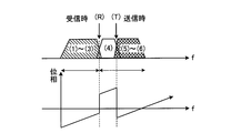
- the frequency vs. phase characteristic of the synthesized signal A ' has discontinuities at the two ⁇ ⁇ (R), (T) ⁇ shown in FIG.
- “ ⁇ ” (R) shown in FIG. 11 represents a discontinuous position generated between the port #n and port # n + 1 (specifically, the reception port # 0 and the reception port # 1) on the reception side as described above.
- “ ⁇ ” (T) shown in FIG. 11 indicates a discontinuous position that occurs between port #n and port # n + 1 (specifically, transmission port # 0 and transmission port # 1) on the transmission side.
- each of the delay circuits 29-1 to 29-N and 33-1 to 33-N in the relay satellite 200 is used in the present embodiment.
- the delay control and the correlation processing in the receiving station 401 a reception sensitivity characteristic equivalent to the case of receiving the original signal A is realized without deterioration of communication quality.
- the processing of the receiving station 401 when the signal A is a spread spectrum signal will be described with reference to FIGS.
- the antenna 500 receives the signal ⁇ A ′, C, D ⁇ , and the amplifier 501 amplifies the level of the signal ⁇ A ′, C, D ⁇ .
- the amplified signal ⁇ A ′, C, D ⁇ is converted from a radio frequency band to an intermediate frequency or baseband via a band pass filter (BPF) 502, a mixer 503, and a low pass filter (LPF) 505. Thereafter, the signal is input to the AD converter 506.
- the AD converter 506, which is a consumer product, samples the signal ⁇ A ′, C, D ⁇ having a total bandwidth of 2 and converts it into a digital signal.
- the demultiplexing unit 507 configured by a consumer digital device Each signal A ′, C, D is demultiplexed from the signal ⁇ A ′, C, D ⁇ of the total bandwidth 2 output from the converter 506.
- the narrowband signal demodulator 508 demodulates the signal C demultiplexed by the demultiplexing unit 507, and the narrowband signal demodulator 509 demodulates the signal D demultiplexed by the demultiplexing unit 507.
- the signals C and D do not cause phase discontinuity in the signal band like the signal A ′. Therefore, in the narrowband signal demodulators 508 and 509, Data demodulation is realized by the demodulation method.
- the broadband signal demodulator 510 performs data demodulation in accordance with correlation processing in accordance with delay control by the relay satellite 200.
- This delay control is to reduce the influence of phase uncertainty that occurs between each port.
- the cross-correlation vector after despreading for each path is received. This is done to separate in the time direction so that communication quality does not deteriorate due to cancellation. Since the correlation vectors separated in the time direction are synthesized by the wideband signal demodulator 510 with the same vector angle, the communication quality does not deteriorate.
- details of the demodulation process will be described.
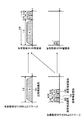
- the control station 110 sets the delay amounts ( ⁇ R0, ⁇ R1, ⁇ T0, ⁇ T1) of the delay circuits 29-1, 29-2, 33-1, 33-2 in the relay satellite 200, for example, as shown in FIG. . Since the control station 110 manages this satellite system such as all the control of the relay satellite 200, the type of each signal to be relayed, the frequency arrangement, etc., each delay set for the relay satellite 200 as necessary. Information useful for demodulating the signal A ′, such as the value and the phase discontinuity position (R), (T) of the signal A ′, is also notified to the receiving station 401.
- FIG. 12A shows an example of delay processing for the signal A on the receiving side of the relay satellite 200
- FIG. 12B shows an example of delay processing for the signal A on the transmitting side of the relay satellite 200.
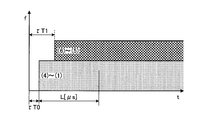
- each delay time is set to a small value with respect to the spreading code length L [ ⁇ sec].
- the signal (( ⁇ (1), (2), (3), (4), (5), (6) ⁇ )) 1), (2), and (3) are given a time delay ⁇ R0 (0 [second] in this example) by the delay circuit 29-1, and the signals (4), (5), and (6) are the delay circuit 29- 2 gives a time delay ⁇ R1 (FIG. 12A).
- the signals (1), (2), (3), (4) are given a time delay ⁇ T0 by the delay circuit 33-1, and the signals (5), (6) are delayed.
- Circuit 33-2 provides a time delay ⁇ T1.
- the relay satellite 200 finally gives the signal A the delay shown in FIG.
- the wideband signal demodulator 510 of the receiving station 401 After performing the delay setting, the wideband signal demodulator 510 of the receiving station 401 starts the despreading process in the cross-correlation unit 511.
- the cross-correlation unit 511 obtains a cross-correlation with the signal A ′ using a known despreading code at a sampling period several times the chip rate for spreading (performs a sliding correlation).
- FIGS. 13A and 13B show examples of cross-correlation characteristics.
- (A) shows the cross-correlation vector characteristic
- (b) shows the cross-correlation power characteristic.
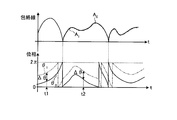
- the cross-correlation power is 1 when any one of the signals ⁇ (1), (2), (3), (4), (5), (6) ⁇ is received, as shown in FIG.
- the cross-correlation vector (power amount: 3) by the signal ⁇ (1), (2), (3) ⁇ , and after the time ( ⁇ R0 + ⁇ T1), the cross-correlation vector (power amount: power): 1) After time ( ⁇ R1 + ⁇ T1), a cross-correlation vector (amount of power: 2) based on the signals ⁇ (5), (6) ⁇ is obtained.
- the vector phase detector 512 determines the number of cross-correlation vectors shown in FIG. 13A, the arrival time of each vector, and each vector from the cross-correlation data series (FIG. 13A) obtained by the cross-correlator 511. The phase angle is detected and notified to the synthesis unit 513.
- the vector phase detector 512 detects each delay amount ( ⁇ R0, ⁇ R1, ⁇ T0, ⁇ T1) collected from the control station 110 when the vector arrival time or vector phase angle is detected, and the phase discontinuity position of the signal A ′.
- the number of vectors to be detected (three in this example), the expected value of the ratio of vector lengths (3: 1: 2 in this example), the time difference between the vectors (in this example, ⁇ T1 ⁇ T0, ⁇ R1 ⁇
- Each information of ( ⁇ R0 + ⁇ T1- ⁇ T0) may be used. In this case, the number of vectors, the arrival time of the vector, and the vector phase angle can be detected more accurately than in the case of detecting without using such information.
- the synthesizer 513 uses each information of the number of vectors detected by the vector phase detector 512, the arrival time of the vector, and the vector phase angle to calculate each correlation vector of the cross-correlation data series output from the cross-correlator 511. Vector composition and output.
- the cross-correlation data series is input to delay units 600 and 601 and adder 620.
- the delay unit 600 performs time delay control for matching the first path vector that arrives first with the arrival time of the third path. Specifically, based on the time difference information of the vector detected by vector phase detection unit 512, vector phase detection unit 512 provides delay device 600 with the delay amount ( ⁇ R1- ⁇ R0 + ⁇ T1- ⁇ T0) of the first path.
- the delay unit 601 performs time delay control for matching the second path vector to the arrival time of the third path. Specifically, based on the vector time difference information detected by the vector phase detector 512, the vector phase detector 512 gives the delay amount of the second path ( ⁇ R1- ⁇ R0) to the delay device 601.
- the positions of the three correlation vectors shown in FIG. 13 can be aligned with the vector positions of the third path by each delay control process of the cross-correlation data series branched in three. However, since the correlation vector phase angles are not aligned, the vector phase angles are also aligned by the following processing.
- the phase shifter 610 matches the vector phase angle of the first path that arrives first with the vector phase angle of the third path. Specifically, based on the vector phase angle information detected by the vector phase detector 512, the vector phase detector 512 gives the phase shift amount of the first path to the phase shifter 610. Similarly, the phase shifter 611 matches the vector phase angle of the second path with the vector phase angle of the third path. Specifically, the vector phase detection unit 512 gives the phase shift amount of the second path to the phase shifter 611.
- the vector phase angles of the three-branched cross correlation data series can all be aligned with the vector position of the third path.
- the adder 620 adds the three cross-correlation data series subjected to the above-described time delay control and phase shift control, and the latch 630 performs the addition based on the arrival time of the vector detected by the vector phase detection unit 512. From the cross-correlation data series, a correlation peak value after vector synthesis is extracted.
- the combined signal vectors output from the combining unit 513 are aligned as shown in FIG. 14, so that a signal with 6 electric energy can be obtained without a decrease in signal level.
- the downstream detection unit 514 receives the combined signal vector output from the combining unit 513 at the spreading code period (L [ ⁇ s]) as an input, performs synchronous detection or delay detection, and demodulates the data.
- each path Since the cross-correlation vectors after despreading can be separated in the time direction so as to cancel each other at the time of reception and the communication quality does not deteriorate, good communication quality can be realized at the time of cross-correlation vector synthesis.
- the relay satellite receives a processing block for receiving a signal from the transmitting station (a set of ⁇ BPF, mixer, LPF, A / D, delay circuit, demultiplexing shown in FIG. And a processing block for transmitting a signal to the receiving station (a set of ⁇ multiplexing unit, delay circuit, D / A, LPF, mixer, BPF ⁇ shown in FIG. 3)
- N reception processing blocks are used and N reception processing blocks are used.
- the block performs reception processing of input wideband signals in parallel for different frequency components and receives each signal received using N reception processing blocks using a plurality of transmission processing blocks.
- each processing block (reception processing block, transmission processing block) gives a delay with a different delay amount for each processing block. did.
- a signal including a broadband signal exceeding the performance limit (bandwidth 1) of the space device can be relayed, and a flexible relay operation can be realized.
- the digital switch matrix unit that relays signals between the reception processing block and the transmission processing block receives a plurality of signals (signals demultiplexed by each reception block in the previous stage) having the same receiving destination (relay destination) receiving station.
- the signal type whether it is a wideband signal or a non-wideband signal
- the total bandwidth is allocated in consideration of being less than or equal to the bandwidth that can be processed by each transmission processing block in the subsequent stage. Can be realized.
- the reception port # 0 path or the reception port # 1 path is faulty or an unexpected interference wave is input, so that the reception port # 0 or the reception port Even if the input of # 1 is saturated and normal received signal processing cannot be realized, the other normal path is used, and communication is not interrupted. Can be relayed.
- the reception port # 1 fails, half of the wideband signal A (signals (4), (5), (6)) is lost, so the second correlation vector ( The power 1) and the third correlation vector (power 2) disappear.
- the first correlation vector (power 3) obtained via the reception port # 0 can be received, the reception characteristic falls within a range of 3 dB (half). For example, the transmission data rate is increased by 0.5 times. Communication can be established by the adaptive modulation control to be dropped.
- the delay control in the relay satellite 200 may not be performed in order to simplify the relay satellite 200 and the satellite communication system. That is, the relay satellite 200 may be configured without the delay circuits 29-1 to 29-N and 33-1 to 33-N. In this case, since the delay difference of each path in the relay satellite 200 is less than one chip, the cross-correlation vector phase angle of each path cancels out, so that communication quality may be deteriorated. Therefore, the relay satellite 200 and the satellite communication system can be simplified in configuration.
- Embodiment 2 the signal processing example in the case where the signal A is a spread spectrum signal has been described.
- the signal A may not be a spread spectrum signal but may be, for example, a wideband PSK modulated signal that does not perform spread spectrum.
- the broadband transmitting station 101 transmits the broadband PSK modulated signal with a transmission path equalizing preamble added thereto.
- the relay satellite 200 relays the broadband signal A by the same processing as in the first embodiment.
- FIG. 16 is a diagram illustrating a configuration example of the receiving station 401 (wideband PSK receiving station) in the second embodiment.
- a receiving station 401 includes an antenna 500, an amplifier 501, a band pass filter 502, a mixer 503, a reception local generation unit 504, a low pass filter 505, an AD converter (A / D) 506, A demultiplexing unit 507, a wideband signal demodulator 510a, and narrowband signal demodulators 508 and 509 are provided.
- Broadband signal demodulator 510 a includes cross-correlation section 521, transmission path estimation section 522, equalization section 523, and detection section 524. That is, the receiving station 401 of this embodiment is obtained by replacing the wideband signal demodulator 510 of the receiving station 401 (see FIG. 4) described in Embodiment 1 with a wideband signal demodulator 510a. The part is the same. Therefore, in the present embodiment, only the operation of wideband signal demodulator 510a will be described.
- the cross-correlation unit 521 performs a cross-correlation process between the received signal A and the known preamble using the same preamble added to the wideband PSK modulation signal (see FIG. 15).
- the transmission path estimation unit 522 extracts the cross-correlation characteristics between the preamble included in the received signal A and the known preamble from the cross-correlation data sequence obtained by the cross-correlation processing by the cross-correlation unit 521 by detecting the cross-correlation power. Then, the extracted cross-correlation characteristic is stored as a transmission path estimation value.
- the equalization unit 523 performs equalization processing of the received signal A using the transmission path estimated value. For example, after the transmission path estimation value and the reception signal A are converted from the time domain to the frequency domain, the reception signal A converted to the frequency domain is divided by the transmission path estimation value converted to the frequency domain. The equalization process is performed. By this equalization processing, the frequency vs. phase characteristics in the signal A band, for example, even if the discontinuity shown in FIG. Processing can correct phase discontinuities. The data series after division is again converted from the frequency domain to the time domain in the equalization unit 523 and then output to the detection unit 524.
- the detection unit 524 may demodulate the signal A (wideband PSK modulation signal) by a general demodulation process because the phase discontinuity in the signal A band is eliminated by the equalization process in the equalization unit 523.
- the satellite communication system including the relay satellite 200 not only the spread spectrum signal described in the first embodiment but also the relay of the wideband PSK modulation signal without performing the spread spectrum can be realized with a good communication quality. I can do it.
- relay satellite 200 may not be performed in this embodiment in order to simplify the relay satellite 200 and the satellite communication system. That is, the relay satellite 200 may be configured without the delay circuits 29-1 to 29-N and 33-1 to 33-N.
- Embodiment 3 FIG.
- the reception analog switch matrix unit 22 performs connection control of signals from the reception antennas 21-1 to 21-N to the reception ports. ), (2), the reception analog switch matrix unit 22 may be eliminated, and the configuration of the relay satellite 200 may be simplified.
- each of the receiving antennas 21-1 to 21-N is made variable by a command from the control station 110.
- the relay satellite 200 not only the reception antenna 21-1, but also the reception antenna 21-2 is controlled to be directed to the wideband beam area 100, so that the wideband signal A is received by the reception port # as in the first embodiment. 0 and receiving port # 1 can be processed.
- the receiving antenna 21-3 By directing the receiving antenna 21-3 to the narrowband beam area 102, the signals B, C, and D received by the receiving antenna 21-3 are processed by the receiving port # 2 as in the first embodiment. I can do it.
- the transmission analog switch matrix unit 39 controls connection of signals from each transmission port to the transmission antennas 40-1 to 40-N.
- the following (3) By adopting (4), the transmission analog switch matrix unit 39 may be eliminated, and the configuration of the relay satellite 200 may be simplified.
- each of the transmission antennas 40-1 to 40-N is made variable by a command from the control station 110.
- the transmission antenna 40-1 not only the transmission antenna 40-1 but also the transmission antenna 40-2 is controlled to be directed to the beam area 400, so that the transmission port # 0 (BPF 38-1) is the same as in the first embodiment. ) And the transmission port # 1 (BPF 38-2), that is, wideband signals ⁇ A ′, C, D ⁇ can be transmitted to the ground receiving station 401.
- the signal B output from the transmission port # 2 (BPF 38-3) can be transmitted to the ground receiving station 403.
- Embodiment 4 the phase discontinuity generated in the relay satellite 200 is compensated by the ground receiving station 401.
- the relay satellite 200 itself has a phase generated on the receiving side. Discontinuity is compensated by digital signal processing.
- the number of phase discontinuities is reduced from two (R and T) shown in FIG. 11 to one (T). Can do.
- phase discontinuity that has occurred on the receiving side of the relay satellite is eliminated, so that the complexity of the processing amount of the ground receiving station 401 is reduced, and the frequency utilization efficiency of the uplink This improves the capacity of existing transmitting / receiving stations.
- details will be described.
- the configuration on the transmission side of the relay satellite 200 of the present embodiment is the same as that of FIG. 3 of the first embodiment.
- the configuration on the receiving side is the configuration in which the delay circuits 29-1, 29-2, 29-3,..., 29-N are excluded from the configuration of FIG. That is, in this embodiment, in FIG. 2, the outputs of the AD converters 28-1, 28-2, 28-3,..., 28-N are separated from the demultiplexers 30-1, 30-2, 30-3. ,..., 30-N.
- a new process not performed in the first embodiment is performed inside the digital switch matrix unit 31. Details of this processing will be described later.
- terrestrial receiving station 401 in the present embodiment when receiving a spread spectrum signal, terrestrial receiving station 401 in the present embodiment eliminates the second path. Therefore, delay unit 601 and phase shifter 611 are excluded from the combining unit shown in FIG. It becomes the composition. Other than this, there is no structural difference between the receiving station 401 of the present embodiment and the receiving station 401 of the first or second embodiment.
- the operation of the satellite communication system of the present embodiment will be described. As in the first embodiment, an example of operation in the case of receiving a signal from broadband transmitting station 101 and signals from narrowband transmitting stations 103, 104, and 105 and transmitting the signals to receiving stations 401 and 403 will be described. To do.
- the signals from the transmitting stations 101, 103, 104, and 105 are demultiplexed by the demultiplexing units 30-1, 30-2, 30-3,..., 30-N of the relay satellite 200 (receiving side).
- a series of processing up to this point is the same as in the first embodiment except that each signal is no longer delayed due to the deletion of the delay circuit. That is, signals (1), (2), (3) from the receiving port # 0 are signals (4), (5), (6) from the receiving port # 1, and signals B, C, D is input to the digital switch matrix unit 31 of the present embodiment.
- FIG. 17 shows a configuration example of the digital switch matrix unit 31 of the present embodiment.
- the digital switch matrix unit 31 of the present embodiment includes a phase compensation unit 700 and a switch unit 701.
- Phase compensation unit 700 includes delay adjustment units 702 and 705, frequency conversion units 703 and 706, low-pass filters 704 and 707, complex multiplier 708, limiter 709, autocorrelation detection unit 710, and path delay difference detection. 711 and complex multipliers 712, 713, 714 and 715.
- the reception section signal output from the demultiplexing unit 30-1 for handling an input signal from the receive port # 0 (see FIG. 2) (1) is input to the terminal # 0 1 according FIG.
- signals output from the demultiplexing unit 30-1 (2) to the terminal # 0 2 the signal (3) is input to the terminal # 0 3.
- the signal output from the demultiplexing unit 30-2 for handling an input signal from the receive port # 1 (4) is input to the terminal # 1 0 according Figure 17.
- signals output from the demultiplexing unit 30-2 (5) to a terminal # 1 1, the signal (6) is input to the terminal # 1 2.
- FIG. 18 is a diagram illustrating an example of processing of the phase compensation unit 700 included in the digital switch matrix unit 31 according to the present embodiment.
- the phase compensation unit 700 includes signals ⁇ (1), (2), (3) ⁇ output from the demultiplexing unit 30-1 of the receiving unit and signals ⁇ (4) output from the demultiplexing unit 30-2. , (5), (6) ⁇ is compensated for.
- the switch unit 701 receives the signals ⁇ (1), (2), (3) ⁇ , ⁇ (4), (5), (6) ⁇ compensated by the phase compensation unit 700 and inputs the signals from the first embodiment. Similarly, the switch processing shown in FIG. 10 is performed together with the signals ⁇ B, C, D ⁇ that are not subject to phase compensation.
- phase compensation unit 700 half of the wideband signal A passes through the reception port # 0 and the other half passes through the reception port # 1, but only a part of overlapping signal components pass through both ports. To do. Specifically, it is the overlap region shown in FIG. 18, and this common signal component is part of the signal (3) (shaded portion) output from the demultiplexing unit 30-1 as shown in FIG. It is included in a part (shaded portion) of the signal (4) output from the demultiplexing unit 30-2.
- the overlap component included in a part of the signal (3) is extracted by the low-pass filter 704 after the signal (3) is converted to baseband (0 Hz) by the frequency converter 703 shown in FIG.
- the overlap component included in a part of the signal (4) is extracted by the low-pass filter 707 after the signal (4) is converted into the baseband (0 Hz) by the frequency converter 706.
- the signals (3) and (4) are delay-adjusted by the delay adjustment units 702 and 705 in the previous stage and then input to the frequency conversion units 703 and 706. The operation regarding delay adjustment will be described later.
- the overlap component extracted by the low-pass filter 704 is indicated by S 0
- the overlap component extracted by the low-pass filter 707 is indicated by S 1 .
- the signal components ⁇ S 0 , S 1 ⁇ all match the signal vectors at the respective sampling points in the time direction, that is, ⁇ S 0 , S 1 ⁇ have the same waveform.
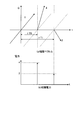
- FIG. 19 shows the envelope and phase of the signal component ⁇ S 0 , S 1 ⁇ when the phase difference ⁇ occurs.
- FIG. 19 is a diagram illustrating an example of a relationship between the same components (respective overlap components extracted by the low-pass filters 704 and 707) of the reception signals input to two different reception ports (reception ports # 0 and # 1). is there.
- a 0 envelope signal overlap component S 0 is, theta 0 phase signal overlap component S 0 is, A 1 is the envelope signal overlap component S 1, ⁇ 1 is overlap component S 1 Phase signal.
- FIG. 20 shows the envelope signal ⁇ A 0 , A 1 ⁇ and the phase signal ⁇ 0 , ⁇ 1 ⁇ of the signal ⁇ S 0 , S 1 ⁇ when the path delay difference ⁇ occurs.
- the envelope signal A 1 is input with a delay of ⁇ with respect to the envelope signal A 0 .
- phase difference of the phase signals ⁇ 0 , ⁇ 1 ⁇ is not constant and varies as is apparent from FIG.
- the phase difference changes from moment to moment, such as at times t1 and t2 in FIG.
- the phase is present between the signal input to reception port # 0 and the reception signal input to reception port # 1 in phase compensation unit 700 using the above-described property. Compensates for discontinuities and path delay differences. Hereinafter, this compensation operation will be described.
- the complex multiplier 708 performs complex multiplication on the signal S 0 and the complex conjugate value of the signal S 1 .
- the vector angle ⁇ corresponds to the phase difference ⁇ between the reception port # 0 and the reception port # 1.
- the path delay difference detection unit 711 obtains the path delay difference ⁇ using this property.
- the path delay difference detection unit 711 intentionally gives a delay difference between each path in units of time Tc by outputting an instruction signal for adjusting the delay amount to the delay adjustment units 702 and 705 in the previous stage.
- FIG. 21 shows an operation example of the path delay difference detection unit 711.
- the autocorrelation power becomes the highest (P +1 in the figure) when “+ Tc” is set that is closest to the actual path delay difference ⁇ .
- the delay difference setting at which the autocorrelation power is the second highest is “0” (P 0 in the figure), and it can be seen that the actual path delay difference ⁇ exists as a peak value between 0 and + Tc. .
- the delay adjustment units 702 and 705 are composed of, for example, polyphase filters, and perform fine sampling phase adjustment on input data based on the delay adjustment signals ⁇ 1 , ⁇ 2 ⁇ from the path delay difference detection unit 711. Do. Specifically, the delay adjustment unit 702 gives a common delay ⁇ 1 to each demultiplexed data from the demultiplexing unit 30-1 and outputs the demultiplexed data. Similarly, the delay adjustment unit 705 gives a common delay ⁇ 2 to each demultiplexed data from the demultiplexing unit 30-2 and outputs the demultiplexed data.
- the path delay difference detection unit 711 fixes the delay adjustment signal ⁇ 2 for the delay adjustment unit 705 to ⁇ 0 ⁇ and The delay adjustment signal ⁇ 1 is given by ⁇ 0, Tc, 2Tc,.
- the path delay difference detection unit 711 performs delay adjustment while fixing the delay adjustment signal ⁇ 1 for the delay adjustment unit 702 to ⁇ 0 ⁇ .
- the delay adjustment signal ⁇ 2 is given to the unit 705 as ⁇ 0, Tc, 2Tc,.
- the path delay difference detection unit 711 performs the following control on the delay adjustment units 702 and 705.
- the path delay difference detection unit 711 When ⁇ is positive, the path delay difference detection unit 711 gives the delay adjustment signal ⁇ 2 to the delay adjustment unit 705 as ⁇ while setting the delay adjustment signal ⁇ 1 for the delay adjustment unit 702 to ⁇ 0 ⁇ . This cancels the path difference in the positive direction.
- the path delay difference detection unit 711 sets the delay adjustment signal ⁇ 1 to the delay adjustment unit 702 to ⁇ while setting the delay adjustment signal ⁇ 2 for the delay adjustment unit 705 to ⁇ 0 ⁇ . By giving it, the path difference in the negative direction is negated.
- the path delay difference detection unit 711 corrects the path difference by the two-stage processing flow of “detection mode” and “correction mode”.
- the phase compensation unit 700a of the digital switch matrix unit 31a illustrated in FIG. 22 has a configuration in which dedicated delay adjustment units 716 and 717 for detecting a path difference are added to the phase compensation unit 700 illustrated in FIG. ing.
- the delay adjustment units 716 and 717 are used for detecting ⁇ , and the delay adjustment units 702 and 705 are used for delay adjustment of each demultiplexed data.
- a delay adjusting unit 716 in accordance with the delay adjustment signal tau '1 from the path delay difference detection unit 711 delays the signal (3) which is input from the terminal # 0 3.
- the delay adjusting unit 717 in accordance with the delay adjustment signal tau '2 from the path delay difference detection unit 711 delays the signal (4) which is input from the terminal # 1 0.
- the path delay difference detection unit 711 controls the delay adjustment units 716 and 717 to give the path delay difference by ⁇ ..., ⁇ 2Tc, ⁇ Tc, 0, + Tc, + 2Tc,.
- the path delay difference can be corrected from moment to moment without stopping.
- the delay adjustment units 702 and 705 are provided inside the phase compensation unit 700a, but may be moved to the previous stage of each port. For example, it may be moved to the previous stage of the demultiplexing units 30-1 and 30-2 in the receiving unit (see FIG. 2).
- delay adjustment is performed before the demultiplexing units 30-1 and 30-2, it is only necessary to perform delay adjustment for one signal before demultiplexing for each port. Therefore, when delay adjustment is performed for each signal after demultiplexing Compared to the above, there is an advantage that the circuit scale and the calculation amount are reduced.
- the path delay difference detection unit 711 performs control to cancel ( ⁇ + ⁇ ) based on the initial control value ⁇ and the newly detected variation ⁇ . 702 and 705 are performed.
- the limiter 709 converts the length of the signal vector output from the complex multiplier 708 into a constant value. That is, the limiter 709 limits the amplitude of the signal vector input from the complex multiplier 708 on the unit circle, thereby removing the amplitude information included in the input signal and allowing only the phase information to pass.
- complex multipliers 712, 713, 714, and 715 and the conjugate value of the complex signal output from limiter 709 and each signal (demultiplexed by demultiplexing unit 30-1 and delayed by delay adjusting unit 702) Each signal after the path delay difference is corrected is subjected to complex multiplication.
- the signal vector phases of the signals ⁇ (1), (2), (3) ⁇ demultiplexed by the demultiplexing unit 30-1 are corrected by ⁇ and demultiplexed by the demultiplexing unit 30-2.
- the phase discontinuity between the waved signals ⁇ (4), (5), (6) ⁇ and the signals ⁇ (1), (2), (3) ⁇ corrected by ⁇ is eliminated.
- Subsequent processing of the relay satellite 200 is the same as that of the first embodiment, and the signal ⁇ A, C, D ⁇ is transmitted to the receiving station 401 and the signal B is transmitted to the receiving station 403.
- phase compensation processing in the phase compensation unit 700 eliminates (R) occurring at the time of reception out of the two phase discontinuities (R) and (T) shown in FIG. 11, and transmission is performed as shown in FIG. It becomes one place of the phase discontinuity point (T) at the time.
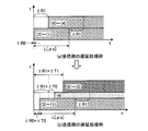
- the delay circuits 29-1, 29-2, 29-3,..., 29-N of the receiving unit provided in the relay satellite 200 are removed, as shown in FIG.
- the time delay difference is given between signals (1) to (4) output from transmission port # 0 and signals (5) to (6) output from transmission port # 1 during transmission. Therefore, as shown in FIG. 25, terrestrial receiving station 401 only needs to synthesize two-wave correlation vectors, so the amount of processing is reduced compared to the case where three waves are synthesized as in the first embodiment. it can.
- the upper limit of the signal bandwidth that can be processed by a set of ⁇ AD converter, demultiplexer, multiplexer, DA converter ⁇ in the relay satellite 200 is set.
- the bandwidth of the wideband signal A is 1.5.
- this signal A is demultiplexed into the signals ⁇ (1), (2), (3), (4) ⁇ shown in FIG.
- phase discontinuity occurs between signals (3) and (4) during reception.
- no phase discontinuity occurs due to the compensation processing performed by the phase compensators 700 and 700a.
- the wideband signal A can be demodulated even by an existing terrestrial receiving station that does not perform special signal processing. That is, if switching control is performed to avoid the phase discontinuity that occurs on the transmission side, the signals on the reception side of the relay satellite 200, that is, the uplink signals, have a total bandwidth of 2.0 processed by the port # 0 and the port # 1. The frequency utilization efficiency of the uplink can be improved, and the capacity of existing transmitting / receiving stations can be increased.
- the relay satellite 200 itself compensates for the phase discontinuity generated on the reception side of the relay satellite by digital signal processing, so that the processing complexity in the ground receiving station 401 is reduced.
- the effect of reducing the amount of processing and the effect of increasing the capacity of the existing system can be obtained.
- phase compensation between port # 0 and port # 1 has been described.
- phase discontinuity between other ports such as port # 1 and port # 2, port # 2 and port # 3, etc. are also compensated in the same way. Therefore, when the number of ports is N, the phase compensators 700 and 700a are required to have a maximum of N ⁇ 1.
- the frequency conversion units 703 and 706, the low-pass filters 704 and 707, the complex multiplier 708, the limiter 709, the autocorrelation detection unit 710, and the path delay difference detection unit 711 are time-division when the time variation of the phase difference or path difference is slow. By using it, the size may be reduced. In this case, since the circuit for obtaining the phase difference and path difference between the ports is shared by one, the scale of the circuit for obtaining the phase difference and path difference is reduced to 1 / (N-1) times.
- Embodiment 5 aims to realize better demodulation performance by changing the processing of the receiving station 401 on the ground.
- the combining unit 513 (see FIG. 4 and FIG. 5) of the receiving station 401 in Embodiment 1 sets the positions of the three correlation vectors shown in FIG.
- each correlation vector includes not only three signal vectors indicating a solid peak value, but also a plurality of dotted lines before and after. A correlation vector is obtained. Therefore, if the combining unit 513 combines not only the three points corresponding to the peak value of each correlation vector but also the respective correlation vectors before and after that, it is possible to realize even better demodulation performance.
- the vector position detecting unit 512 detects each of K vectors
- the combining unit 513 includes K ⁇ 1 delay units, K ⁇ 1. And an adder and a latch for vector synthesis of K cross-correlation data after delay and phase shift.
- Embodiment 6 FIG. In the sixth embodiment, a configuration example in the case where digital beam forming (DBF) is combined will be described.
- DBF digital beam forming
- This embodiment solves the problem that when a beam is formed by digital signal processing by DBF, broadband signal relay cannot be realized due to the performance limit of a space device.
- FIG. 27 is a diagram illustrating an internal configuration example of a receiving unit that performs processing on the receiving side in the relay satellite according to the sixth embodiment.
- the same components as those of the receiving unit (see FIG. 2) described in the first embodiment are denoted by the same reference numerals.
- the receiving unit of the present embodiment has a configuration in which receiving DBF processing units 80-1, 80-2,... Are added between the delay circuit 29 and the demultiplexing unit 30.
- codes are added by embodying each component of port 3 (bandpass filter 23-4, mixer 24-4, lowpass filter 27-4, A / D 28-4, delay circuit 29-4). is doing.
- FIG. 28 is a diagram illustrating an internal configuration example of a transmission unit that performs processing on the transmission side in the relay satellite according to the sixth embodiment.
- the same components as those of the transmission unit (see FIG. 3) described in the first embodiment are denoted by the same reference numerals.
- the transmission unit of the present embodiment has a configuration in which transmission DBF processing units 90-1, 90-2,... Are added between the multiplexing unit 32 and the delay circuit 33.
- symbols are added by embodying each component of port 3 (delay circuit 33-4, D / A 34-4, low-pass filter 35-4, mixer 36-4, band-pass filter 38-4). is doing.
- the relay satellite 200 uses the receiving antennas 21-1 and 21-2 as element antennas, and forms a beam directed to the wideband beam area 100 with these two element antennas.
- the broadband signal A is received.
- the reception analog switch matrix unit 22 connects the signal of the reception antenna 21-1 to the port # 0 and the port # 1, and connects the signal of the reception antenna 21-2 to the port # 2 and the port # 3.
- the operations of the bandpass filter 23-1, the mixer 24-1, the lowpass filter 27-1, the A / D 28-1, and the delay circuit 29-1 that perform processing on the signal input from the port # 0 are described in the first embodiment. It is the same. That is, a signal in the lower half of the wideband signal A received by the receiving antenna 21-1 is extracted.
- a band pass filter 23-3, a mixer 24-3, a low pass filter 27-3, an A / D 28-3, and a delay circuit 29-3 that process the signal input from the port # 2 are input from the port # 0.
- the same processing as that performed on the received signal is executed, and the signal on the lower half of the wideband signal A received by the receiving antenna 21-2 is extracted.
- the delay amount of the delay circuit 29-3 is set to the same ⁇ R0 as the delay amount of the delay circuit 29-1.
- the band pass filter 23-2, the mixer 24-2, the low pass filter 27-2, the A / D 28-2, and the delay circuit 29-2 that process the signal input from the port # 1 are connected to the above ports.
- the same processing as that of each component that processes the signal input from # 0 is performed, and the signal on the high frequency side half of the broadband signal A received by the receiving antenna 21-1 is extracted.
- the band-pass filter 23-4, the mixer 24-4, the low-pass filter 27-4, the A / D 28-4, and the delay circuit 29-4 that perform processing on the signal input from the port # 3 are as described above.
- the same processing as that of each component that processes the signal input from the port # 2 is performed, and the high-frequency half signal of the broadband signal A received by the receiving antenna 21-2 is extracted.
- the delay amount of the delay circuit 29-4 is set to the same ⁇ R1 as the delay amount of the delay circuit 29-2.
- the reception DBF processing unit 80-1 executes the following processes [1], [2], and [3] to generate a low frequency side component of the wideband signal A. [1] The low-frequency component of the signal A input from the delay circuit 29-1 is multiplied by the weight value W1 for the receiving antenna 21-1. [2] The low frequency component of the signal A input from the delay circuit 29-3 is multiplied by the weight value W2 for the receiving antenna 21-2. [3] The multiplication results obtained by executing the processes [1] and [2] are added.
- the reception DBF processing unit 80-2 performs the following processes [4], [5], and [6] to generate a high frequency component of the wideband signal A.
- the high frequency side component of the signal A input from the delay circuit 29-2 is multiplied by the weight value WR1 for the receiving antenna 21-1.
- the high frequency side component of the signal A input from the delay circuit 29-4 is multiplied by the weight value WR2 for the receiving antenna 21-2.
- the multiplication results obtained by executing the processes [4] and [5] are added.
- the subsequent processing is the same as in the first embodiment.
- the demultiplexing unit 30-1 demultiplexes the low-frequency component of the wideband signal A
- the demultiplexing unit 30-2 demultiplexes the high-frequency component of the wideband signal A. To wave.
- the relay satellite 200 uses the transmission antennas 40-1 and 40-2 as element antennas, forms a beam directed to the beam area 400 with these two element antennas, and transmits the broadband signal A to the reception station 401.
- the transmission analog switch matrix unit 39 connects signals from Port # 0 and Port # 1 to the transmission antenna 40-1, and connects signals from Port # 2 and Port # 3 to the transmission antenna 40-2.
- the processing of the multiplexing units 32-1 and 32-2 is the same as in the first embodiment. That is, the multiplexing unit 32-1 combines the signals (1), (2), (3), and (4) shown in FIG. 10 and outputs the signal (c) shown in FIG. Further, the multiplexing unit 32-2 multiplexes the signals (5) and (6) shown in FIG. 10 and outputs the signal (D) shown in FIG.
- the transmission DBF processing unit 90-1 performs the following processes [7] and [8], and generates two low frequency component signals S1-1 and S1-2. [7] The signal input from the multiplexing unit 32-1 is multiplied by the weight value WT1 for the antenna element 40-1, and is output as the low-frequency component signal S1-1. [8] The signal input from the multiplexing unit 32-1 is multiplied by the weight value WT2 for the antenna element 40-2 and output as a low-frequency component signal S1-2.
- the transmission DBF processing unit 90-2 performs the following processes [9] and [10] to generate two high frequency component signals S2-1 and S2-2. [9] The signal input from the multiplexing unit 32-2 is multiplied by the weight value WT1 for the antenna element 40-1, and is output as the high frequency component signal S2-1. [10] The signal input from the multiplexing unit 32-2 is multiplied by the weight value WT2 for the antenna element 40-2, and is output as a high-frequency component signal S2-2.
- the delay circuit 33-1, D / C 34-1, low-pass filter 35-1, mixer 36-1, and band-pass filter 38-1 are as follows: The same processing as in the first embodiment is performed on the low frequency component signal S1-1 output from the transmission DBF processing unit 90-1, and the low frequency component of the signal transmitted from the transmission antenna 40-1 is generated. To do.
- the delay circuit 33-2, D / C 34-2, low-pass filter 35-2, mixer 36-2, and band-pass filter 38-2 include a high-frequency component signal S2- output from the transmission DBF processing unit 90-2. 1, the same processing as in the first embodiment is performed to generate a high-frequency component of the signal transmitted from the transmitting antenna 40-1.
- the delay circuit 33-3, D / C 34-3, low-pass filter 35-3, mixer 36-3, and band-pass filter 38-3 are supplied with the low-frequency component signal S1 output from the transmission DBF processing unit 90-1.
- -2 is processed in the same manner as in Embodiment 1 to generate a low-frequency component of the signal transmitted from the transmitting antenna 40-2.
- the delay circuit 33-4, D / C 34-4, low-pass filter 35-4, mixer 36-4, and band-pass filter 38-4 are high-frequency component signals S2-output from the transmission DBF processing unit 90-2. 2, the same processing as in the first embodiment is executed to generate a high-frequency component of the signal transmitted from the transmitting antenna 40-2.
- the relay satellite 200 of the present embodiment forms a beam to the beam area 400 and, similarly to the first embodiment, transmits the wideband signal A ′ to which the delay difference is given to the receiving station 401. Send.
- the receiving station 401 performs the same processing as in the first embodiment and demodulates the received wideband signal A ′.
- the broadband signal A when the broadband signal A is relayed by DBF by satellite, a configuration in which the low frequency side of the broadband signal is processed and the multiple ports that process the high frequency side are shared and relayed. Therefore, even when DBF is applied, a space device having a low sampling speed can be applied. Furthermore, it is possible to realize high-speed beam pattern switching peculiar to DBF and increase in antenna gain.
- the number of antenna elements may be three or more. In this case, when the number of elements of the reception antenna or transmission antenna is N, the number of ports of the relay satellite 200 is 2N.
- the relay satellite 200 has been described with one reception beam (broadband beam area 100) and one transmission beam (beam area 400).
- the number of reception beams and the number of transmission beams is two or more. But it ’s okay.
- each reception DBF processing unit (reception DBF processing units 80-1 and 80-2) generates M reception beam signals from N pieces of input element data. That is, the reception DBF processing units 80-1 and 80-2 multiply the input N element data by N weight values used for forming one beam and then add all the results to the reception signal of the corresponding beam. Are output simultaneously for M beams.
- each transmission DBF processing unit (transmission DBF processing units 90-1 and 90-2) generates N output element data from M transmission beam signals.
- the transmission DBF processing units 90-1 and 90-2 perform a process of duplicating N transmission beam signals and multiplying each of the duplicated transmission beam signals by N weight values. Run at the same time. Furthermore, the transmission DBF processing units 90-1 and 90-2 generate and output N pieces of output element data by adding all signals addressed to the same transmission antenna.
- the DBF process and the ⁇ demultiplexing process / combining process ⁇ are combined as an example of operation.
- only the DBF process may be performed to relay the signal.
- the function of performing the frequency rearrangement of each signal at the time of satellite relay is lost, and only the satellite connects between the beams, but the demultiplexing units 30-1 and 30-2 and the multiplexing unit 32- 1 and 32-2 are not required, and the digital switch matrix section can be realized with a small circuit scale because it has a simple configuration for simply connecting the beams.
- the relay satellite according to the present invention is useful when constructing a satellite communication system, and in particular, relays even a broadband signal that exceeds the performance limit of the device constituting the satellite (space device). It is suitable for a relay device of a satellite communication system that can do this.
Abstract
Description
本実施の形態では、広帯域信号を、低いサンプリング速度、処理速度のデバイスを用いて中継することが可能な中継衛星、および衛星通信システムについて説明する。
<1>広帯域ビームエリア100内の広帯域送信局101からの広帯域信号Aを、ビームエリア400内の受信局401へ送信
<2>狭帯域ビームエリア102内の狭帯域送信局103からの狭帯域信号Bを、ビームエリア402内の受信局403へ送信
<3>狭帯域ビームエリア102内の狭帯域送信局104からの狭帯域信号Cを、ビームエリア400内の受信局401へ送信
<4>狭帯域ビームエリア102内の狭帯域送信局105からの狭帯域信号Dを、ビームエリア400内の受信局401へ送信
実施の形態1では、信号Aがスペクトラム拡散信号である場合の信号処理例を示したが、信号Aはスペクトラム拡散信号でなく、例えば、スペクトラム拡散を行わない広帯域PSK変調信号としても良い。この場合、広帯域送信局101は、図15に示すように、広帯域PSK変調信号に伝送路等化用のプリアンブルを付加した形で送信する。中継衛星200は実施の形態1と同様の処理で、本広帯域信号Aを中継する。
実施の形態1の中継衛星200では、受信アナログスイッチマトリックス部22が、各受信アンテナ21-1~21-Nからの信号を、各受信ポートに接続制御する例を示したが、以下の(1),(2)とすることで、受信アナログスイッチマトリックス部22を無くした構成とし、中継衛星200の構成を簡易化しても良い。
(2)受信アンテナを、受信ポートと同じ数だけ確保し、各受信アンテナと各受信ポートを1対1で直結する。例えば、図2において、受信アンテナ21-nと受信ポート#n-1(n=1,2,…,N)を直結する。
(4)送信アンテナを、送信ポートと同じ数だけ確保し、各送信アンテナと各送信ポートを1対1で直結する。例えば、図3において、送信アンテナ40-nと送信ポート#n-1(n=1,2,…,N)を直結する。
実施の形態1~3では、中継衛星200で生じた位相不連続を、地上の受信局401で補償する構成としていたが、本実施の形態では、中継衛星200自らが、受信側で生じた位相不連続をデジタル信号処理で補償する。詳細については後述するが、位相不連続を中継装置200において補償する本実施の形態によれば、位相不連続点を図11に示す2箇所(RとT)から1箇所(T)に減らすことができる。また、本実施の形態では、中継衛星の受信側で生じていた位相不連続が解消されるため、地上の受信局401の処理量の複雑さが軽減される効果や、アップリンクの周波数利用効率が向上し、既存の送受信局の収容性が高まる効果も得られる。以降、詳細について説明する。
実施の形態5では、地上の受信局401の処理を変更することで、更に良好な復調性能を実現することを目的としている。
実施の形態6では、デジタルビームフォーミング(DBF:Digital Beam Forming)を組合せた場合の構成例について説明する。
[1]遅延回路29-1から入力される信号Aの低域側成分に、受信アンテナ21-1用のウエイト値W1を乗算する。
[2]遅延回路29-3から入力される信号Aの低域側成分に、受信アンテナ21-2用のウエイト値W2を乗算する。
[3]処理[1],[2]を実行して得られた各乗算結果を加算する。
[4]遅延回路29-2から入力される信号Aの高域側成分に、受信アンテナ21-1用のウエイト値WR1を乗算する。
[5]遅延回路29-4から入力される信号Aの高域側成分に、受信アンテナ21-2用のウエイト値WR2を乗算する。
[6]処理[4],[5]を実行して得られた各乗算結果を加算する。
[7]合波部32-1から入力される信号に、アンテナ素子40-1用のウエイト値WT1を乗算し、低域成分信号S1-1として出力する。
[8]合波部32-1から入力される信号に、アンテナ素子40-2用のウエイト値WT2を乗算し、低域成分信号S1-2として出力する。
[9]合波部32-2から入力される信号に、アンテナ素子40-1用のウエイト値WT1を乗算し、高域成分信号S2-1として出力する。
[10]合波部32-2から入力される信号に、アンテナ素子40-2用のウエイト値WT2を乗算し、高域成分信号S2-2として出力する。
22 受信アナログスイッチマトリックス部
23-1,23-2,23-3,23-N バンドパスフィルタ(BPF)
24-1,24-2,24-3,24-N ミキサ
25 受信ローカル生成部
26 原振
27-1,27-2,27-3,27-N ローパスフィルタ(LPF)
28-1,28-2,28-3,28-N AD変換器(A/D)
29-1,29-2,29-3,29-N 遅延回路
30-1,30-2,30-3,30-N 分波部
31,31a デジタルスイッチマトリックス部
32-1,32-2,32-3,32-N 合波部
33-1,33-2,33-3,33-N 遅延回路
34-1,34-2,34-3,34-N DA変換器(D/A)
35-1,35-2,35-3,35-N ローパスフィルタ(LPF)
36-1,36-2,36-3,36-N ミキサ
37 送信ローカル生成部
38-1,38-2,38-3,38-N バンドパスフィルタ(BPF)
39 送信アナログスイッチマトリックス部
40-1,40-2,40-N 送信アンテナ
80-1,80-2 受信DBF処理部
90-1,90-2 送信DBF処理部
100 広帯域ビームエリア
101 広帯域送信局
102 狭帯域ビームエリア
103,104,105 狭帯域送信局
110 制御局
200 中継衛星
400,402 ビームエリア
401,403 受信局
500 アンテナ
501 アンプ
502 バンドパスフィルタ(BPF)
503 ミキサ
504 受信ローカル生成部
505 ローパスフィルタ(LPF)
506 AD変換器(A/D)
507 分波部
508,509 狭帯域信号用復調器
510,510a 広帯域信号用復調器
511,521 相互相関部
512 ベクトル位相検出部
513 合成部
514,524 検波部
522 伝送路推定部
523 等化部
600,601 遅延器
610,611 移相器
620 加算器
700,700a 位相補償部
701 スイッチ部
702,705,716,717 遅延調整部
703,706 周波数変換部
704,707 ローパスフィルタ
708,712,713,714,715 複素乗算器
709 リミタ
710 自己相関検出部
711 経路遅延差検出部
Claims (16)
- 複数の受信アンテナと、
複数の受信処理手段と、
複数の送信処理手段と、
複数の送信アンテナと、
前記複数の受信アンテナそれぞれで受信した信号を前記受信処理手段の1つまたは2つ以上に出力する第1のスイッチ手段と、
前記複数の受信処理手段それぞれが受信処理を行って得られたデジタル受信信号を前記送信処理手段の1つまたは2つ以上に出力する第2のスイッチ手段と、
前記複数の送信処理手段それぞれが送信処理を行って得られたアナログ信号を前記送信アンテナの1つに出力する第3のスイッチ手段と、
を備え、
前記第1のスイッチ手段は、前記受信処理手段で処理が可能な帯域よりも広帯域の受信信号が入力された場合、当該広帯域受信信号を複数の受信処理手段に出力し、
前記受信処理手段は、自身で処理可能な帯域よりも広帯域の信号が入力された場合、当該入力信号の一部の帯域を対象として受信処理を行うことを特徴とする中継衛星。 - 前記複数の受信アンテナと前記複数の受信処理手段を1対1で接続し、
前記受信アンテナを指向性が調整可能なアンテナとするとともに、前記第1のスイッチ手段を省略した構成としたことを特徴とする請求項1に記載の中継衛星。 - 同一の広帯域受信信号が入力された各受信処理手段は、それぞれ異なる帯域を対象として受信処理を行うことを特徴とする請求項1または2に記載の中継衛星。
- 同一の広帯域受信信号が入力された各受信処理手段におけるそれぞれの処理対象の信号の帯域を、各処理対象の信号を合成した場合に、当該広帯域受信信号と同一帯域となる帯域としたことを特徴とする請求項3に記載の中継衛星。
- 前記受信処理手段は、
自身で処理可能な帯域よりも広帯域の受信信号が入力された場合に自身が処理すべき帯域を抽出するとともに中間周波数信号またはベースバンド信号に変換する処理対象信号抽出手段と、
前記処理対象信号抽出手段から出力された信号をデジタル信号に変換するAD変換手段と、
前記デジタル信号を複数の信号に分波する分波手段と、
を備え、
前記第2のスイッチ手段は、前記分波後の信号を、後段の各送信処理手段で処理可能な帯域に応じて分配することを特徴とする請求項1~4のいずれか一つに記載の中継衛星。 - 前記第2のスイッチ手段は、分配した各信号の送信処理手段ごとの合計帯域が、対応する送信処理手段で処理可能な帯域以下となるように、前記分波後の信号を分配することを特徴とする請求項5に記載の中継衛星。
- 前記受信処理手段は、
前記AD変換手段から出力されたデジタル信号に対して、他の受信処理手段とは異なる値の遅延を与える第1の遅延付加手段、
をさらに備え、
前記分波手段は、前記第1の遅延付加手段により遅延が付加された後の信号を分波し、
前記送信処理手段は、
前記第2のスイッチ手段から入力された各信号を合波する合波手段と、
前記合波後の信号に対して、他の送信処理手段とは異なる値の遅延を与える第2の遅延付加手段と、
前記第2の遅延付加手段から出力された信号をアナログ信号に変換するDA変換手段と、
前記DA変換手段から出力された信号を無線周波数帯信号に変換する変換手段と、
を備えることを特徴とする請求項5または6に記載の中継衛星。 - 前記第2のスイッチ手段は、
同一成分が含まれているデジタル受信信号の間に存在する位相不連続および経路遅延差を補償する補償処理部と、
前記補償処理部で位相不連続および経路遅延差が補償された後のデジタル受信信号を前記送信処理手段の1つまたは2つ以上に出力するスイッチ部と、
を備えることを特徴とする請求項1~6のいずれか一つに記載の中継衛星。 - 前記補償処理部は、
2つのデジタル受信信号の双方に含まれている同一成分の一方に対して他方の複素共役値を周波数領域で複素乗算して相関値を算出する素乗算器と、
前記相関値に基づいて、前記2つのデジタル受信信号の間に存在する経路遅延差を補償する遅延差補償手段と、
前記遅延差補償手段により経路遅延差が補償された後のデジタル受信信号の間に存在する位相不連続を補償する位相補償手段と、
を備えることを特徴とする請求項8に記載の中継衛星。 - ビームフォーミングにより複数の受信ビームを形成する複数の受信アンテナと、
複数の受信処理手段と、
複数の送信処理手段と、
ビームフォーミングにより複数の送信ビームを形成する複数の送信アンテナと、
前記複数の受信アンテナそれぞれで受信した信号を前記受信処理手段の1つまたは2つ以上に出力する第1のスイッチ手段と、
前記複数の受信処理手段それぞれが受信処理を行って得られた複数のデジタル受信信号のうち、同一成分のデジタル受信信号同士を合成する複数の受信信号合成手段と、
前記複数の受信信号合成手段と1対1で対応し、対応する受信信号合成手段から出力された信号を複数の信号に分波する複数の分波手段と、
前記分波手段で分波された後の各信号を前記送信アンテナの1つまたは2つ以上に割り当てる第2のスイッチ手段と、
前記第2のスイッチ手段により同一送信アンテナに割り当てられた各信号を合波する複数の合波手段と、
前記複数の合波手段から出力された各信号を前記複数の受信処理手段の中の2つ以上に分配する分配手段と、
前記複数の送信処理手段それぞれが送信処理を行って得られたアナログ信号のうち、同一成分に基づいて生成された各アナログ信号を、同一送信ビームを形成する異なる送信アンテナに出力する第3のスイッチ手段と、
を備え、
前記第1のスイッチ手段は、前記受信処理手段で処理が可能な帯域よりも広帯域の受信信号が入力された場合、当該広帯域受信信号を複数の受信処理手段に出力し、
前記受信処理手段は、自身で処理可能な帯域よりも広帯域の信号が入力された場合、当該入力信号の一部の帯域を対象として受信処理を行うことを特徴とする中継衛星。 - 請求項1~10のいずれか一つに記載の中継衛星と、
前記中継衛星で中継された信号を受信する受信局と、
を備えることを特徴とする衛星通信システム。 - 請求項7に記載の中継衛星と、
前記中継衛星で中継された信号を受信する受信局と、
を備え、
前記中継衛星は、スペクトラム拡散信号を中継し、
前記受信局は、
前記中継衛星で中継された信号のうち、前記受信処理手段で処理が可能な帯域よりも広帯域の信号を復調するための構成として、
受信信号と既知の逆拡散コードの相互相関を求める相互相関算出手段と、
前記相互相関算出手段による処理で得られた相互相関データ系列に基づいて、当該系列に含まれている相互相関ベクトルの数、各相互相関ベクトルの到来時刻および各相互相関ベクトルの位相角を検出する検出手段と、
前記検出手段による検出結果に基づいて、前記複数の相互相関ベクトルを合成する合成手段と、
前記合成手段により合成された後の相互相関ベクトルに対して検波処理を行う検波手段と、
を備えることを特徴とする衛星通信システム。 - 前記合成手段は、各相互相関ベクトルに対して、各相互相関ベクトルの到来時刻の差に応じた遅延を与えて前記中継衛星の受信処理手段および送信処理手段で個別に付加された遅延量の差をキャンセルするとともに、各相互相関ベクトルの位相角が揃うように調整し、当該調整後の各相互相関ベクトルを加算することを特徴とする請求項12に記載の衛星通信システム。
- 前記合成手段は、受信信号と逆拡散コードの相互相関値のピークを示す相互相関ベクトルおよびピーク前後の所定範囲に含まれる相互相関値を示す相互相関ベクトルを合成することを特徴とする請求項12または13に記載の衛星通信システム。
- 各受信処理手段および各送信処理手段に対して、前記第1の遅延付加手段で与える遅延量および前記第2の遅延付加手段で与える遅延量を指示するとともに、当該指示内容、および当該指示内容に従って中継された信号において位相が不連続となる位置の情報を前記受信局に通知する制御局、
をさらに備え、
前記検出手段は、前記相互相関データ系列および前記制御局からの通知内容に基づいて、前記相互相関ベクトルの数、前記到来時刻および前記位相角を検出することを特徴とする請求項12、13または14に記載の衛星通信システム。 - 前記中継衛星は、スペクトラム拡散が実施されていない変調信号にプリアンブルが付加された信号を中継し、
前記受信局は、
前記中継衛星で中継された信号のうち、前記受信処理手段で処理が可能な帯域よりも広帯域の信号を復調するための構成として、
前記プリアンブルに基づいて伝送路推定を行う伝送路推定手段と、
前記伝送路推定結果に基づいて受信変調信号を等化する等化手段と、
前記等化後の信号に対して検波処理を行う検波手段と、
を備えることを特徴とする請求項11に記載の衛星通信システム。
Priority Applications (3)
| Application Number | Priority Date | Filing Date | Title |
|---|---|---|---|
| US14/111,652 US20140036765A1 (en) | 2011-04-28 | 2012-04-24 | Relay satellite and satellite communication system |
| JP2013512380A JP5372294B2 (ja) | 2011-04-28 | 2012-04-24 | 中継衛星および衛星通信システム |
| EP12777081.6A EP2704337B1 (en) | 2011-04-28 | 2012-04-24 | Relay satellite and satellite communication system |
Applications Claiming Priority (2)
| Application Number | Priority Date | Filing Date | Title |
|---|---|---|---|
| JP2011101854 | 2011-04-28 | ||
| JP2011-101854 | 2011-04-28 |
Publications (1)
| Publication Number | Publication Date |
|---|---|
| WO2012147753A1 true WO2012147753A1 (ja) | 2012-11-01 |
Family
ID=47072271
Family Applications (1)
| Application Number | Title | Priority Date | Filing Date |
|---|---|---|---|
| PCT/JP2012/060995 WO2012147753A1 (ja) | 2011-04-28 | 2012-04-24 | 中継衛星および衛星通信システム |
Country Status (4)
| Country | Link |
|---|---|
| US (1) | US20140036765A1 (ja) |
| EP (1) | EP2704337B1 (ja) |
| JP (1) | JP5372294B2 (ja) |
| WO (1) | WO2012147753A1 (ja) |
Cited By (12)
| Publication number | Priority date | Publication date | Assignee | Title |
|---|---|---|---|---|
| JP2014131164A (ja) * | 2012-12-28 | 2014-07-10 | Mitsubishi Electric Corp | アンテナ装置 |
| WO2014112442A1 (ja) * | 2013-01-15 | 2014-07-24 | 三菱電機株式会社 | 中継装置、中継衛星および衛星通信システム |
| WO2014129038A1 (ja) * | 2013-02-21 | 2014-08-28 | 三菱電機株式会社 | 中継制御局、中継器および干渉抑圧方法 |
| JP5836508B2 (ja) * | 2013-01-15 | 2015-12-24 | 三菱電機株式会社 | 中継装置、中継衛星および衛星通信システム |
| JP5855317B2 (ja) * | 2013-04-18 | 2016-02-09 | 三菱電機株式会社 | 分波装置、合波装置および中継装置 |
| US9749947B2 (en) | 2013-04-19 | 2017-08-29 | Mitsubishi Electric Corporation | Wireless communication apparatus and wireless communication control method that performs communication using a frequency division multiplexing method |
| JP2017532832A (ja) * | 2014-09-04 | 2017-11-02 | エアバス ディフェンス アンド スペイス リミテッド | デジタル信号処理のための拡張可能なアーキテクチャ |
| WO2020158044A1 (ja) * | 2019-01-30 | 2020-08-06 | 三菱電機株式会社 | リソース割当方法、及び通信衛星 |
| JP2021007230A (ja) * | 2015-04-10 | 2021-01-21 | ヴィアサット, インコーポレイテッドViaSat, Inc. | エンドツーエンドビーム形成システム及び衛星 |
| US11258507B2 (en) | 2015-04-10 | 2022-02-22 | Viasat, Inc. | Ground network for end-to-end beamforming |
| US11387894B2 (en) | 2018-02-09 | 2022-07-12 | Mitsubishi Electric Corporation | Satellite receiver and satellite communication system |
| WO2023007630A1 (ja) * | 2021-07-28 | 2023-02-02 | 日本電信電話株式会社 | 無線通信システム、無線通信方法、送信アダプタ装置、及び受信アダプタ装置 |
Families Citing this family (13)
| Publication number | Priority date | Publication date | Assignee | Title |
|---|---|---|---|---|
| US9917634B2 (en) * | 2013-02-14 | 2018-03-13 | Mitsubishi Electric Corporation | Demultiplexing apparatus, multiplexing apparatus, and relay apparatus |
| WO2016195406A2 (ko) * | 2015-06-03 | 2016-12-08 | 주식회사 엘지화학 | 헤테로고리 화합물 및 이를 포함하는 유기 발광 소자 |
| CN106685495A (zh) * | 2015-11-05 | 2017-05-17 | 索尼公司 | 无线通信方法和无线通信设备 |
| WO2017109955A1 (ja) * | 2015-12-25 | 2017-06-29 | 三菱電機株式会社 | 通信衛星、回線制御装置および衛星通信システム |
| US10454567B2 (en) * | 2016-03-02 | 2019-10-22 | Mitsubishi Electric Corporation | Multi-beam satellite communication system |
| US9832007B2 (en) * | 2016-04-14 | 2017-11-28 | Ibiquity Digital Corporation | Time-alignment measurement for hybrid HD radio™ technology |
| US10666416B2 (en) | 2016-04-14 | 2020-05-26 | Ibiquity Digital Corporation | Time-alignment measurement for hybrid HD radio technology |
| US10320712B2 (en) * | 2017-08-17 | 2019-06-11 | The Boeing Company | System and method for configuring a switch matrix on-board a vehicle based on network information |
| US10855366B2 (en) * | 2017-10-10 | 2020-12-01 | Macdonald, Dettwiler And Associates Corporation | Modular channelizer |
| US10756776B2 (en) | 2017-12-01 | 2020-08-25 | Ram Photonics, LLC | Method and system for spread spectrum code acquisition |
| JPWO2020226090A1 (ja) * | 2019-05-09 | 2020-11-12 | ||
| US11569903B2 (en) * | 2020-12-28 | 2023-01-31 | Hughes Network Systems, Llc | Overlay of a forward link on broadband satellite signals |
| CN116094630B (zh) * | 2023-04-07 | 2023-08-08 | 湖南国天电子科技有限公司 | 一种高精度信号延迟计算方法 |
Citations (3)
| Publication number | Priority date | Publication date | Assignee | Title |
|---|---|---|---|---|
| EP0854590A2 (en) * | 1997-01-17 | 1998-07-22 | Com Dev Ltd. | Analog processor for digital satellites |
| JP2006516867A (ja) | 2003-01-28 | 2006-07-06 | ザ・ボーイング・カンパニー | 衛星通信データのデジタル処理のためのシステムおよび方法 |
| JP2011029720A (ja) * | 2009-07-21 | 2011-02-10 | Mitsubishi Electric Corp | 衛星通信装置および衛星通信システム |
Family Cites Families (13)
| Publication number | Priority date | Publication date | Assignee | Title |
|---|---|---|---|---|
| US3095538A (en) * | 1960-10-28 | 1963-06-25 | Silberstein Richard | Satellite relay station using antenna diversity selection |
| US3711855A (en) * | 1969-10-15 | 1973-01-16 | Communications Satellite Corp | Satellite on-board switching utilizing space-division and spot beam antennas |
| DE69229678T2 (de) * | 1991-10-28 | 2000-04-06 | Teledesic Llc Kirkland | Satellitenkommunikationssystem |
| US6307868B1 (en) * | 1995-08-25 | 2001-10-23 | Terayon Communication Systems, Inc. | Apparatus and method for SCDMA digital data transmission using orthogonal codes and a head end modem with no tracking loops |
| JPH1198053A (ja) * | 1997-09-22 | 1999-04-09 | Matsushita Electric Ind Co Ltd | スペクトラム拡散復調回路、スペクトラム拡散通信装置、遅延検波方式復調回路および遅延検波方式通信装置 |
| JP4443939B2 (ja) * | 2004-01-13 | 2010-03-31 | 日本信号株式会社 | 受信時刻計測装置及びこれを用いた距離計測装置 |
| KR100621432B1 (ko) * | 2004-04-21 | 2006-09-08 | 삼성전자주식회사 | 복수의 송신 안테나들을 사용하는 다중셀 직교 주파수분할 다중 방식 통신시스템에서 채널 추정 장치 및 방법 |
| US7747229B2 (en) * | 2004-11-19 | 2010-06-29 | Atc Technologies, Llc | Electronic antenna beam steering using ancillary receivers and related methods |
| US20060223464A1 (en) * | 2005-03-29 | 2006-10-05 | Frank Michael L | Method for switching a power amplifier |
| JP4921378B2 (ja) * | 2005-10-24 | 2012-04-25 | パナソニック株式会社 | 干渉信号特徴量保存方法及び装置、干渉信号特徴量取得方法及び装置、並びに、干渉信号抑圧方法及び装置 |
| US20080064356A1 (en) * | 2006-09-07 | 2008-03-13 | Telefonaktiebolaget Lm Ericsson (Publ) | Method of receiving wideband signal |
| WO2008107710A1 (en) * | 2007-03-03 | 2008-09-12 | Astrium Limited | Satellite beam-pointing error correction in digital beam-forming architecture |
| US8116419B2 (en) * | 2008-07-14 | 2012-02-14 | Alcatel Lucent | Methods and apparatuses for estimating time delay and frequency offset in single frequency networks |
-
2012
- 2012-04-24 WO PCT/JP2012/060995 patent/WO2012147753A1/ja active Application Filing
- 2012-04-24 US US14/111,652 patent/US20140036765A1/en not_active Abandoned
- 2012-04-24 EP EP12777081.6A patent/EP2704337B1/en not_active Not-in-force
- 2012-04-24 JP JP2013512380A patent/JP5372294B2/ja active Active
Patent Citations (3)
| Publication number | Priority date | Publication date | Assignee | Title |
|---|---|---|---|---|
| EP0854590A2 (en) * | 1997-01-17 | 1998-07-22 | Com Dev Ltd. | Analog processor for digital satellites |
| JP2006516867A (ja) | 2003-01-28 | 2006-07-06 | ザ・ボーイング・カンパニー | 衛星通信データのデジタル処理のためのシステムおよび方法 |
| JP2011029720A (ja) * | 2009-07-21 | 2011-02-10 | Mitsubishi Electric Corp | 衛星通信装置および衛星通信システム |
Non-Patent Citations (1)
| Title |
|---|
| See also references of EP2704337A4 * |
Cited By (25)
| Publication number | Priority date | Publication date | Assignee | Title |
|---|---|---|---|---|
| JP2014131164A (ja) * | 2012-12-28 | 2014-07-10 | Mitsubishi Electric Corp | アンテナ装置 |
| WO2014112442A1 (ja) * | 2013-01-15 | 2014-07-24 | 三菱電機株式会社 | 中継装置、中継衛星および衛星通信システム |
| WO2014112040A1 (ja) * | 2013-01-15 | 2014-07-24 | 三菱電機株式会社 | 中継衛星、中継装置および衛星通信システム |
| JP5836508B2 (ja) * | 2013-01-15 | 2015-12-24 | 三菱電機株式会社 | 中継装置、中継衛星および衛星通信システム |
| EP2947788A4 (en) * | 2013-01-15 | 2016-09-07 | Mitsubishi Electric Corp | RELAY DEVICE, RELAY SATELLITE AND SATELLITE COMMUNICATION SYSTEM |
| US9473236B2 (en) | 2013-01-15 | 2016-10-18 | Mitsubishi Electric Corporation | Relay apparatus, relay satellite, and satellite communication system |
| WO2014129038A1 (ja) * | 2013-02-21 | 2014-08-28 | 三菱電機株式会社 | 中継制御局、中継器および干渉抑圧方法 |
| JP5815154B2 (ja) * | 2013-02-21 | 2015-11-17 | 三菱電機株式会社 | 中継制御局、中継器および干渉抑圧方法 |
| JP5855317B2 (ja) * | 2013-04-18 | 2016-02-09 | 三菱電機株式会社 | 分波装置、合波装置および中継装置 |
| EP2988433A4 (en) * | 2013-04-18 | 2016-12-14 | Mitsubishi Electric Corp | DEMULTIPLEXING DEVICE, MULTIPLEXING DEVICE, AND RELAY DEVICE |
| US9749037B2 (en) | 2013-04-18 | 2017-08-29 | Mitsubishi Electric Corporation | Demultiplexing apparatus, multiplexing apparatus, and relay apparatus |
| US9749947B2 (en) | 2013-04-19 | 2017-08-29 | Mitsubishi Electric Corporation | Wireless communication apparatus and wireless communication control method that performs communication using a frequency division multiplexing method |
| JP2017532832A (ja) * | 2014-09-04 | 2017-11-02 | エアバス ディフェンス アンド スペイス リミテッド | デジタル信号処理のための拡張可能なアーキテクチャ |
| JP2021007230A (ja) * | 2015-04-10 | 2021-01-21 | ヴィアサット, インコーポレイテッドViaSat, Inc. | エンドツーエンドビーム形成システム及び衛星 |
| US11258507B2 (en) | 2015-04-10 | 2022-02-22 | Viasat, Inc. | Ground network for end-to-end beamforming |
| US11418254B2 (en) | 2015-04-10 | 2022-08-16 | Viasat, Inc. | Ground network for end-to-end beamforming |
| US11515933B2 (en) | 2015-04-10 | 2022-11-29 | Viasat, Inc. | System and method for return end-to-end beamforming |
| JP7297724B2 (ja) | 2015-04-10 | 2023-06-26 | ヴィアサット,インコーポレイテッド | エンドツーエンドビーム形成システム及び衛星 |
| US11695470B2 (en) | 2015-04-10 | 2023-07-04 | Viasat, Inc. | System and method for return end-to-end beamforming |
| US11843448B2 (en) | 2015-04-10 | 2023-12-12 | Viasat, Inc. | Satellite for end to end beamforming |
| US11387894B2 (en) | 2018-02-09 | 2022-07-12 | Mitsubishi Electric Corporation | Satellite receiver and satellite communication system |
| WO2020158044A1 (ja) * | 2019-01-30 | 2020-08-06 | 三菱電機株式会社 | リソース割当方法、及び通信衛星 |
| JPWO2020158044A1 (ja) * | 2019-01-30 | 2021-10-14 | 三菱電機株式会社 | リソース割当方法、及び通信衛星 |
| JP7154318B2 (ja) | 2019-01-30 | 2022-10-17 | 三菱電機株式会社 | リソース割当方法、及び通信衛星 |
| WO2023007630A1 (ja) * | 2021-07-28 | 2023-02-02 | 日本電信電話株式会社 | 無線通信システム、無線通信方法、送信アダプタ装置、及び受信アダプタ装置 |
Also Published As
| Publication number | Publication date |
|---|---|
| EP2704337A1 (en) | 2014-03-05 |
| US20140036765A1 (en) | 2014-02-06 |
| JP5372294B2 (ja) | 2013-12-18 |
| JPWO2012147753A1 (ja) | 2014-07-28 |
| EP2704337A4 (en) | 2015-05-20 |
| EP2704337B1 (en) | 2019-03-27 |
Similar Documents
| Publication | Publication Date | Title |
|---|---|---|
| JP5372294B2 (ja) | 中継衛星および衛星通信システム | |
| CA2898183C (en) | Relay apparatus, relay satellite, and satellite communication system | |
| JP3338747B2 (ja) | 干渉波除去装置 | |
| KR100312098B1 (ko) | 피드포워드 증폭기 | |
| JP3992489B2 (ja) | 無線通信方法及びその装置 | |
| EP3080929B1 (en) | Phase or amplitude compensation for beam-former | |
| US9231715B2 (en) | I/Q mismatch compensation method and apparatus | |
| WO1998042093A1 (fr) | Dispositif d'etalonnage pour recepteur sans fil d'antenne reseau | |
| JPH1146180A (ja) | アレーアンテナ無線受信装置のキャリブレーション装置 | |
| US9917634B2 (en) | Demultiplexing apparatus, multiplexing apparatus, and relay apparatus | |
| CN101171775A (zh) | 用于上行链路信道的接收装置、接收方法、发送装置以及发送方法 | |
| JP2000013454A (ja) | キャリブレーション装置 | |
| EP1615361B1 (en) | A radio frequency signal receiving apparatus, a radio frequency signal transmitting apparatus, and a calibration method | |
| JP5339450B2 (ja) | 無線通信装置および無線通信方法 | |
| KR20170011906A (ko) | 액티브 어레이 안테나의 캘리브레이션 장치 | |
| WO2019155952A1 (ja) | 衛星受信機、および衛星通信システム | |
| EP3111583A1 (en) | Method and apparatus for high data rate communication | |
| JP5836508B2 (ja) | 中継装置、中継衛星および衛星通信システム | |
| JP3930456B2 (ja) | アレイアンテナ通信装置 | |
| JP2013128224A (ja) | 追尾アンテナ装置および受信系rf特性変動補償方法 | |
| JPH10173580A (ja) | 受信機および受信装置 | |
| JP2020027966A (ja) | 無線通信装置、及び受信信号補正方法 | |
| WO2008029458A1 (fr) | Dispositif de transmission radio, dispositif de réception radio et système de communication sans-fil | |
| JPH03284027A (ja) | ダイバシティ受信装置 | |
| JP2000278055A (ja) | フィードフォワード増幅器 |
Legal Events
| Date | Code | Title | Description |
|---|---|---|---|
| 121 | Ep: the epo has been informed by wipo that ep was designated in this application |
Ref document number: 12777081 Country of ref document: EP Kind code of ref document: A1 |
|
| ENP | Entry into the national phase |
Ref document number: 2013512380 Country of ref document: JP Kind code of ref document: A |
|
| WWE | Wipo information: entry into national phase |
Ref document number: 14111652 Country of ref document: US |
|
| NENP | Non-entry into the national phase |
Ref country code: DE |
|
| WWE | Wipo information: entry into national phase |
Ref document number: 2012777081 Country of ref document: EP |