WO2012144295A1 - 半導体装置 - Google Patents
半導体装置 Download PDFInfo
- Publication number
- WO2012144295A1 WO2012144295A1 PCT/JP2012/057690 JP2012057690W WO2012144295A1 WO 2012144295 A1 WO2012144295 A1 WO 2012144295A1 JP 2012057690 W JP2012057690 W JP 2012057690W WO 2012144295 A1 WO2012144295 A1 WO 2012144295A1
- Authority
- WO
- WIPO (PCT)
- Prior art keywords
- gate wiring
- wiring portion
- gate
- semiconductor device
- power supply
- Prior art date
- Legal status (The legal status is an assumption and is not a legal conclusion. Google has not performed a legal analysis and makes no representation as to the accuracy of the status listed.)
- Ceased
Links
Images









Classifications
-
- H—ELECTRICITY
- H10—SEMICONDUCTOR DEVICES; ELECTRIC SOLID-STATE DEVICES NOT OTHERWISE PROVIDED FOR
- H10D—INORGANIC ELECTRIC SEMICONDUCTOR DEVICES
- H10D62/00—Semiconductor bodies, or regions thereof, of devices having potential barriers
- H10D62/10—Shapes, relative sizes or dispositions of the regions of the semiconductor bodies; Shapes of the semiconductor bodies
- H10D62/124—Shapes, relative sizes or dispositions of the regions of semiconductor bodies or of junctions between the regions
- H10D62/126—Top-view geometrical layouts of the regions or the junctions
- H10D62/127—Top-view geometrical layouts of the regions or the junctions of cellular field-effect devices, e.g. multicellular DMOS transistors or IGBTs
-
- H—ELECTRICITY
- H10—SEMICONDUCTOR DEVICES; ELECTRIC SOLID-STATE DEVICES NOT OTHERWISE PROVIDED FOR
- H10D—INORGANIC ELECTRIC SEMICONDUCTOR DEVICES
- H10D62/00—Semiconductor bodies, or regions thereof, of devices having potential barriers
- H10D62/10—Shapes, relative sizes or dispositions of the regions of the semiconductor bodies; Shapes of the semiconductor bodies
- H10D62/17—Semiconductor regions connected to electrodes not carrying current to be rectified, amplified or switched, e.g. channel regions
- H10D62/393—Body regions of DMOS transistors or IGBTs
-
- H—ELECTRICITY
- H10—SEMICONDUCTOR DEVICES; ELECTRIC SOLID-STATE DEVICES NOT OTHERWISE PROVIDED FOR
- H10D—INORGANIC ELECTRIC SEMICONDUCTOR DEVICES
- H10D64/00—Electrodes of devices having potential barriers
- H10D64/60—Electrodes characterised by their materials
- H10D64/62—Electrodes ohmically coupled to a semiconductor
-
- H—ELECTRICITY
- H10—SEMICONDUCTOR DEVICES; ELECTRIC SOLID-STATE DEVICES NOT OTHERWISE PROVIDED FOR
- H10D—INORGANIC ELECTRIC SEMICONDUCTOR DEVICES
- H10D84/00—Integrated devices formed in or on semiconductor substrates that comprise only semiconducting layers, e.g. on Si wafers or on GaAs-on-Si wafers
- H10D84/01—Manufacture or treatment
- H10D84/0123—Integrating together multiple components covered by H10D12/00 or H10D30/00, e.g. integrating multiple IGBTs
- H10D84/0126—Integrating together multiple components covered by H10D12/00 or H10D30/00, e.g. integrating multiple IGBTs the components including insulated gates, e.g. IGFETs
- H10D84/0165—Integrating together multiple components covered by H10D12/00 or H10D30/00, e.g. integrating multiple IGBTs the components including insulated gates, e.g. IGFETs the components including complementary IGFETs, e.g. CMOS devices
- H10D84/0186—Manufacturing their interconnections or electrodes, e.g. source or drain electrodes
-
- H—ELECTRICITY
- H10—SEMICONDUCTOR DEVICES; ELECTRIC SOLID-STATE DEVICES NOT OTHERWISE PROVIDED FOR
- H10D—INORGANIC ELECTRIC SEMICONDUCTOR DEVICES
- H10D84/00—Integrated devices formed in or on semiconductor substrates that comprise only semiconducting layers, e.g. on Si wafers or on GaAs-on-Si wafers
- H10D84/01—Manufacture or treatment
- H10D84/02—Manufacture or treatment characterised by using material-based technologies
- H10D84/03—Manufacture or treatment characterised by using material-based technologies using Group IV technology, e.g. silicon technology or silicon-carbide [SiC] technology
- H10D84/038—Manufacture or treatment characterised by using material-based technologies using Group IV technology, e.g. silicon technology or silicon-carbide [SiC] technology using silicon technology, e.g. SiGe
-
- H—ELECTRICITY
- H10—SEMICONDUCTOR DEVICES; ELECTRIC SOLID-STATE DEVICES NOT OTHERWISE PROVIDED FOR
- H10D—INORGANIC ELECTRIC SEMICONDUCTOR DEVICES
- H10D89/00—Aspects of integrated devices not covered by groups H10D84/00 - H10D88/00
- H10D89/10—Integrated device layouts
-
- H—ELECTRICITY
- H10—SEMICONDUCTOR DEVICES; ELECTRIC SOLID-STATE DEVICES NOT OTHERWISE PROVIDED FOR
- H10W—GENERIC PACKAGES, INTERCONNECTIONS, CONNECTORS OR OTHER CONSTRUCTIONAL DETAILS OF DEVICES COVERED BY CLASS H10
- H10W20/00—Interconnections in chips, wafers or substrates
- H10W20/40—Interconnections external to wafers or substrates, e.g. back-end-of-line [BEOL] metallisations or vias connecting to gate electrodes
- H10W20/41—Interconnections external to wafers or substrates, e.g. back-end-of-line [BEOL] metallisations or vias connecting to gate electrodes characterised by their conductive parts
- H10W20/427—Power or ground buses
-
- H—ELECTRICITY
- H10—SEMICONDUCTOR DEVICES; ELECTRIC SOLID-STATE DEVICES NOT OTHERWISE PROVIDED FOR
- H10W—GENERIC PACKAGES, INTERCONNECTIONS, CONNECTORS OR OTHER CONSTRUCTIONAL DETAILS OF DEVICES COVERED BY CLASS H10
- H10W72/00—Interconnections or connectors in packages
-
- H—ELECTRICITY
- H10—SEMICONDUCTOR DEVICES; ELECTRIC SOLID-STATE DEVICES NOT OTHERWISE PROVIDED FOR
- H10D—INORGANIC ELECTRIC SEMICONDUCTOR DEVICES
- H10D84/00—Integrated devices formed in or on semiconductor substrates that comprise only semiconducting layers, e.g. on Si wafers or on GaAs-on-Si wafers
- H10D84/80—Integrated devices formed in or on semiconductor substrates that comprise only semiconducting layers, e.g. on Si wafers or on GaAs-on-Si wafers characterised by the integration of at least one component covered by groups H10D12/00 or H10D30/00, e.g. integration of IGFETs
- H10D84/82—Integrated devices formed in or on semiconductor substrates that comprise only semiconducting layers, e.g. on Si wafers or on GaAs-on-Si wafers characterised by the integration of at least one component covered by groups H10D12/00 or H10D30/00, e.g. integration of IGFETs of only field-effect components
- H10D84/83—Integrated devices formed in or on semiconductor substrates that comprise only semiconducting layers, e.g. on Si wafers or on GaAs-on-Si wafers characterised by the integration of at least one component covered by groups H10D12/00 or H10D30/00, e.g. integration of IGFETs of only field-effect components of only insulated-gate FETs [IGFET]
- H10D84/85—Complementary IGFETs, e.g. CMOS
Definitions
- the present invention relates to a semiconductor device, and more particularly to a semiconductor device applied to a logic circuit.
- a plurality of cells are combined with one inverter circuit as one cell.
- the power supply wiring and the ground wiring that are spaced apart from each other extend in the X-axis direction.
- An n-channel field effect transistor and a p-channel field effect transistor are connected in series between the ground wiring and the power supply wiring.
- the gate wiring portion extends in the Y-axis direction orthogonal to the X-axis direction.
- the cell size is indicated by pitch and grid.
- the pitch is the length in the X-axis direction
- the grid is the length in the Y-axis direction.
- the length of one pitch and the length of one grid are the same length.
- one pitch is the minimum pitch of the first wiring, and is a length obtained by combining the wiring width of the first wiring and the interval between the first wirings adjacent to each other.
- the conventional inverter circuit cells include a 3-pitch 9-grid cell or a 3-pitch 7-grid cell.
- the minimum pitch of the first wiring is 360 nm
- the length in the X-axis direction is 1080 nm ( 360 nm ⁇ 3)
- the length in the Y-axis direction is 2520 nm (360 nm ⁇ 7).
- Patent Document 1 Japanese Patent Application Laid-Open No. 11-330461
- Patent Document 2 Japanese Patent Application Laid-Open No. 05-198593
- JP 11-330461 A Japanese Patent Laid-Open No. 05-198593
- the present invention has been made as part of its development, and an object thereof is to provide a semiconductor device capable of reducing the size of cells constituting a logic circuit.
- a semiconductor device is a semiconductor device including an inverter circuit in which complementary switching elements are connected in series between a power supply potential and a ground potential, the semiconductor substrate having a main surface, and a power supply A power supply wiring to which a potential is applied, a ground wiring to which a ground potential is applied, an element formation region for a complementary switching element, and a gate wiring portion are included.
- the power supply wiring is formed on the surface of the semiconductor substrate and extends in parallel with the first direction.
- the ground wiring is formed on the surface of the semiconductor substrate, and extends parallel to the first direction at a distance from the power supply wiring in a second direction orthogonal to the first direction.
- the element formation regions are respectively defined by element isolation insulating films in the region of the semiconductor substrate sandwiched between the power supply wiring and the ground wiring.
- the gate wiring portion is formed so as to cross the element formation region.
- the gate wiring portion includes a first gate wiring portion and a second gate wiring portion.
- the first gate wiring portion is formed in parallel to the second direction from one side to the other side where the power supply wiring and the ground wiring are respectively arranged, and extends to a predetermined position in the element formation region.
- the second gate wiring portion is formed in parallel to a third direction obliquely intersecting the second direction from the first gate wiring portion to the other side, and between the element formation region and the element isolation insulating film. As a boundary, it extends so as to straddle a boundary parallel to the first direction.
- a semiconductor device includes a semiconductor substrate having a main surface, an element formation region, and a gate wiring portion.
- the element formation region is defined by an element isolation insulating film in the semiconductor substrate.
- the gate wiring portion is formed so as to cross the element formation region.
- the gate wiring portion includes a first gate wiring portion and a second gate wiring portion.
- the first gate wiring portion is formed in a direction orthogonal to the direction in which the boundary extends toward the boundary between the element formation region and the element isolation insulating film, and extends to a predetermined position in the element formation region. .
- the second gate wiring portion is bent from the first gate wiring portion and extends so as to cross the boundary diagonally.
- the area of the semiconductor device can be reduced by reducing the cell size.
- the area of the semiconductor device can be reduced by reducing the size of the cell.
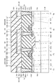
- FIG. 3 is a cross-sectional view taken along a cross-sectional line III-III shown in FIG. 2 in the same embodiment.
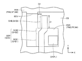
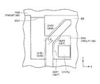
- FIG. 4 is a partially enlarged plan view showing a gate wiring portion and its periphery in the same embodiment. It is a top view which shows the cell of the inverter circuit in the semiconductor device which concerns on a comparative example.
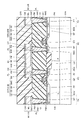
- FIG. 8 is a sectional view taken along section line VIII-VIII shown in FIG. 7 in the embodiment.
- FIG. 4 is a partially enlarged plan view showing a gate wiring portion and its periphery in the same embodiment.
- it is a top view for comparing the size of the cell of the inverter circuit which concerns on the embodiment, and the cell of the inverter circuit which concerns on a comparative example.
- FIG. 12 is a cross sectional view taken along a cross sectional line XII-XII shown in FIG. 11 in the embodiment.
- FIG. 4 is a partially enlarged plan view showing a gate wiring portion and its periphery in the same embodiment. In the embodiment, it is a top view for comparing the size of the cell of the inverter circuit which concerns on the embodiment, and the cell of the inverter circuit which concerns on a comparative example.
- FIG. 12 is a cross sectional view taken along a cross sectional line XII-XII shown in FIG. 11 in the embodiment.
- FIG. 4 is a partially enlarged plan view showing a gate wiring portion and its periphery in the same embodiment. In the embodiment, it is a top view for comparing the size of the cell of the inverter circuit which concerns on the embodiment, and the cell of the inverter circuit which concerns on a comparative example.
- FIG. 12 is a cross sectional view taken along a cross sectional line XII-X
- FIG. 11 is a plan view showing a gate design pattern of the gate wiring body according to the second embodiment for explaining optical proximity effect correction related to a mask pattern for patterning the gate wiring body in the gate wiring part in the embodiment.
- the optical proximity effect correction is applied to the gate design pattern of the gate wiring body according to the second embodiment for explaining the optical proximity effect correction related to the mask pattern for patterning the gate wiring body in the gate wiring portion. It is a top view which shows the performed gate mask pattern.
- FIG. 10 is a plan view showing a gate design pattern of the gate wiring body according to the third embodiment for explaining optical proximity effect correction related to a mask pattern for patterning the gate wiring body in the gate wiring part in the same embodiment; .
- the optical proximity effect correction is applied to the gate design pattern of the gate wiring body according to the third embodiment to explain the optical proximity effect correction related to the mask pattern for patterning the gate wiring body in the gate wiring portion.
- FIG. 5 is a partially enlarged plan view showing an example of a reference gate mask pattern when optical proximity effect correction is performed on the gate design pattern of the gate wiring body in the embodiment. In the same embodiment, it is a top view which shows the array which has arrange
- FIG. 5 is a first partial enlarged plan view showing an example of a gate mask pattern obtained by further correcting the reference gate mask pattern by the arrangement pattern of the gate wiring portion in the embodiment.
- FIG. 10 is a second partial enlarged plan view showing an example of a gate mask pattern obtained by further correcting the reference gate mask pattern by the arrangement pattern of the gate wiring portion in the embodiment.
- inverter circuit which is a basic (unit) for constructing a logic circuit, as shown in FIG. 1, a p-channel field effect transistor QP and an n-channel type transistor are provided between a power supply potential (Vcc) and a ground potential.
- a field effect transistor QN is connected in series.
- a semiconductor device including a gate wiring portion capable of reducing the cell size of the inverter circuit INV will be specifically described.
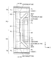
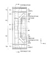
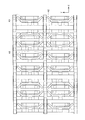
- Embodiment 1 In the first embodiment, a semiconductor device in which a gate wiring portion is bent twice will be described. As shown in FIGS. 2 and 3, two element formation regions PER and NER (active regions) that are electrically insulated from each other by the element isolation insulating film EB are defined on the surface of the semiconductor substrate SUB in the cell of the inverter circuit. Has been. In one element formation region PER, an N well NW is formed from the surface to a predetermined depth. In the other element formation region NER, a P well PW is formed from the surface thereof to a predetermined depth.
- a tap portion TA to which a power supply potential is applied and a p-channel region PC in which a channel of a p-channel field effect transistor is formed are formed.
- N + impurity region NT is formed from the surface of N well NW to a predetermined depth.
- the tap part TA is formed in a region immediately below the power supply line VM which will be described later.
- a tap portion TB to which a ground potential is applied and an n channel region NC in which a channel of an n channel type field effect transistor is formed are formed.
- a P + impurity region PT is formed from the surface of the P well PW to a predetermined depth.
- the tap portion TB is formed directly below the ground wiring EM described later.
- the gate wiring portion GHB is formed so as to cross the element formation region PER and the element formation region NER.
- a gate wiring body GH of a polysilicon film having a thickness of about 200 nm is formed on the gate insulating film GZ having a thickness of about 3 nm.
- the width (gate length direction) of the gate wiring body GH is, for example, about 100 nm.
- a metal silicide film GMS such as cobalt silicide having a film thickness of about 15 nm is formed on the upper surface of the gate wiring body GH.
- a sidewall insulating film GS having a film thickness of about 60 nm made of a laminated film of a silicon oxide film and a silicon nitride film is formed.
- the length of each of the element formation region PER and the element formation region NER in the Y-axis direction is, for example, 0.4 ⁇ m.
- the portion of the gate wiring portion GHB that crosses the element formation region PER is the gate electrode portion GEP of the p-channel field effect transistor QP. Further, in the element formation region PER, one side portion and the other side portion across the gate electrode portion GEP are respectively provided with a P + impurity region PF serving as a source / drain from the surface over a predetermined depth. Is formed.
- the portion of the gate wiring portion GHB that crosses the element formation region NER becomes the gate electrode portion GEN of the n-channel field effect transistor QN. Further, in the element formation region NER, the portion on one side and the portion on the other side across the gate electrode portion GEN have N + impurity regions NF to be a source and a drain over a predetermined depth from the surface, respectively. Is formed.
- a metal silicide film PMS such as a cobalt silicide film is formed on the surface of the N + impurity region NT located in the tap portion TA and the surface of the P + impurity region PF located in the p channel region PC.
- a metal silicide film NMS such as a cobalt silicide film is also formed on the surface of the P + impurity region PT located in the tap portion TB and the surface of the N + impurity region NF located in the n-channel region NC.
- a first interlayer insulating film DF1 having a thickness of about 500 nm is formed on the semiconductor substrate SUB so as to cover the gate wiring portion GHB by a chemical mechanical polishing process.
- a contact hole CH exposing the metal silicide film NMS is formed in the portion of the first interlayer insulating film DF1 located in the tap portion TA.
- a contact hole CH exposing the metal silicide film NMS is formed in the portion of the first interlayer insulating film DF1 located in the p-channel region PC.
- a contact hole CH exposing the metal silicide film PMS is formed in the portion of the first interlayer insulating film DF1 located in the tap portion TB.
- a contact hole CH exposing the metal silicide film PMS is formed in the portion of the first interlayer insulating film DF1 located in the n channel region NC.
- a plug PL including a barrier metal layer BM1 and a buried metal layer PM is formed.
- the barrier metal layer BM1 for example, titanium nitride having a thickness of about 10 nm is laminated on titanium having a thickness of 10 nm.
- tungsten is formed as the metal layer PM.
- a power supply wiring VM to which a power supply potential is applied is formed on the surface of the portion of the first interlayer insulating film DF1 located in the tap portion TA.
- the power supply wiring VM is electrically connected to one source / drain (metal silicide film PMS) of the p-channel field effect transistor through the plug PL.
- a power supply potential (for example, 1.5 V) is applied to N well NW by power supply wiring VM.
- a ground wiring EM to which a ground potential is applied is formed on the surface of the portion of the first interlayer insulating film DF1 located in the tap portion TB.
- the ground wiring is electrically connected to one source / drain (metal silicide film NMS) of the n-channel field effect transistor through the plug PL.
- a ground potential (0 V) is applied to the P well PW by the ground wiring EM.
- the power supply wiring VM and the ground wiring EM each extend in parallel in the X-axis direction (first direction). Further, the power supply wiring VM and the ground wiring EM are spaced from each other in the Y-axis direction orthogonal to the X-axis.
- First metal interconnection M1 is formed to extend between the surface of the portion of first interlayer insulating film DF1 located in p channel region PC and the surface of the portion of first interlayer insulating film DF1 located in n channel region NC.
- the first metal wiring M1 connects the other source / drain (metal silicide film PMS) of the p-channel field effect transistor and the other source / drain (metal silicide film NMS) of the n-channel field effect transistor to the plug PL. Electrical connection through
- Each of the power supply wiring VM, the ground wiring EM, and the first metal wiring M1 has a structure in which a barrier metal layer BM2, a metal layer ML, and a cap metal layer CM are laminated.
- a barrier metal layer BM2 for example, titanium nitride having a thickness of about 20 nm is laminated on titanium having a thickness of 10 nm.
- the metal layer ML for example, an aluminum film having a thickness of about 220 nm is formed.
- the cap metal layer CM for example, titanium nitride having a thickness of about 20 nm is laminated on titanium having a thickness of 10 nm.
- a second interlayer insulating film DF2 is formed on the first interlayer insulating film DF1 so as to cover the power supply wiring VM, the ground wiring EM, and the first metal wiring M1.
- the gate wiring part GHB includes a first gate wiring part GHB1 including a first gate electrode part GEB1, a second gate wiring part GHB2 including a second gate electrode part GEB2, and a third gate wiring part. GHB3.
- the first gate wiring portion GHB1 including the first gate electrode portion GEB1 is formed in parallel to the Y-axis direction (second direction) toward the power supply wiring VM and extends to a predetermined position in the element formation region PER. is doing.
- the second gate wiring portion GHB2 including the second gate electrode portion GEB2 is formed in parallel to a direction (third direction) bent obliquely with respect to the Y-axis direction from the first gate wiring portion GHB1 to the power supply wiring VM side. Thus, it extends so as to straddle the boundary between the element formation region PER and the element isolation insulating film EB, which is parallel to the X-axis direction (first direction).
- the third gate wiring portion GHB3 further extends in parallel with the Y-axis direction (second direction) from the second gate wiring portion GHB2 to the power supply wiring VM side.
- the portion of the gate wiring portion GHB that crosses the element formation region NER is similar to the portion that crosses the element formation region PER, and the first gate wiring portion GHB1, the second gate wiring portion GHB2, and the third Gate wiring portions (see FIG. 2) respectively corresponding to the gate wiring portions GHB3 are provided.
- the cell size of the inverter circuit can be made smaller than the cell size of the conventional inverter circuit by bending the gate wiring portion GHB. This will be described.
- element formation regions JPER and JNER are respectively defined by the element isolation insulating film JEB.
- the power supply wiring JVM and the ground wiring extend in the X-axis direction with a space therebetween.
- a gate wiring portion JGHB is formed in the Y-axis direction orthogonal to the X-axis direction. In the gate wiring portion JGHB, the portion crossing the element forming region JPER that becomes the gate electrode portion JGEP and the portion crossing the element forming region JNER that becomes the gate electrode portion JGEN extend in parallel to the Y-axis direction without bending.
- the gate wiring portion JGHB is electrically connected to the first metal wiring JM1 through the plug JPL.
- the power supply wiring JVM is electrically connected to one source / drain (metal silicide film JPMS) of the p-channel type field effect transistor JQP via the plug JPL.
- the ground wiring JEM is electrically connected to one source / drain (metal silicide film JNMS) of the n-channel field effect transistor JQN through the plug JPL.
- the other source / drain (metal silicide film JPMS) of the p-channel field effect transistor JQP and the other source / drain (metal silicide film JNMS) of the n-channel field effect transistor JQN are connected to the first metal wiring JM1. And electrically connected via a plug JPL.
- two first metal wirings JM1 are formed in parallel to the Y-axis direction with a gap therebetween.
- a plug JPL that electrically connects one first metal wiring JM1 and the gate wiring portion JGHB is formed.
- a plug JPL is formed to electrically connect the other first metal wiring JM1 and the source / drain of each of the two field effect transistors JQP and JQN.
- a length (three pitches) of three times the pitch of the first metal wiring JM1 is required in the X-axis direction.
- the pitch is a minimum pitch of the first metal wiring, and is a length obtained by combining the wiring width of the first metal wiring and the interval between the first metal wirings adjacent to each other.
- a length of 6 grids is required in the Y-axis direction. The length of one grid is the same as the length of one pitch.
- the gate wiring portion JGHB has a predetermined wiring width or the like (shape) in order to exhibit desired performance as a field effect transistor. It is necessary to cross the formation region JPER and the element formation region JNER.
- the wiring width of the gate wiring portion JGHB may be increased or decreased due to variations in manufacturing of the semiconductor device. Moreover, the position may shift. In view of such manufacturing variations, as shown in FIG. 5, in the gate wiring portion JGHB, beyond the element formation region JPER, beyond the boundary between the element formation region JPER and the element isolation insulating film JEB, It is necessary to extend a predetermined length (length JD1) on the element isolation insulating film JEB. The same applies to the gate wiring portion JGHB crossing the element formation region JNER because of the symmetry of the pattern.
- the extension part (length JD1) of the gate wiring part JGHB has the following restrictions.
- the element forming region JPER located immediately below the power supply wiring JVM and the element forming region JPER where the channel of the field effect transistor JQP is formed cover the N + impurity region NJT and the P + impurity region JPF.
- a metal silicide film JPMS is formed on the surface. That is, the metal silicide film JPMS is formed so as to cover the boundary between the N + impurity region JNT and the P + impurity region JPF, which is called a batting diffusion JBDV (JBDE).
- the gate wiring portion JGHB (the extended portion (length JD1) of the gate wiring portion JGHB) is formed so as to overlap the batting diffusion in a planar manner due to manufacturing variations of the semiconductor device
- the metal The region (width) of the silicide film JPMS is further narrowed, and there is a concern about disconnection of the metal silicide film JPMS. This is similarly a concern for the batting diffusion JBDE due to the symmetry of the pattern.
- the extended portion (length JD1) of the gate wiring portion JGHB is planarly formed on the portion of the element formation region JPER where the batting diffusion is located. In order not to overlap, it is necessary that the distance between the two is separated by a predetermined distance JD2. Therefore, in the semiconductor device according to the comparative example, it is not easy to reduce the length of the cell of the inverter circuit, particularly in the X-axis direction.
- the gate wiring portion GHB includes the first gate wiring portion GHB1, the second gate wiring portion GHB2, and the third gate wiring portion GHB3. ing.
- the second gate wiring portion GHB2 is formed in parallel to a direction (third direction) bent obliquely with respect to the Y-axis direction from the first gate wiring portion GHB1 to the power supply wiring VM side. It extends so as to straddle the boundary between the element formation region PER and the element isolation insulating film EB, which is parallel to the (first direction).
- the third gate wiring portion GHB3 further extends in parallel with the Y-axis direction (second direction) from the second gate wiring portion GHB2 to the power supply wiring VM side.
- the length JXL in the X-axis direction is 3 pitches and the length JYL in the Y-axis direction is 7 grids.
- the length XL in the X-axis direction is 2 pitches
- the length YL in the Y-axis direction is 6 grids
- the area occupied by the cells of the inverter circuit is about 57. % Can be reduced.
- the semiconductor device according to the comparative example of 3 pitches and 7 grids has a length in the X axis direction of 1080 nm (360 nm ⁇ 3) and a length in the Y axis direction. Is 2520 nm (360 nm ⁇ 7).
- the length in the X-axis direction is 720 nm (360 nm ⁇ 2)
- the length in the Y-axis direction is 2160 nm (360 nm ⁇ 6).
- the gate wiring portion GHB does not overlap the element forming region PER in plan view, so that there is no concern that the metal silicide film PMS is disconnected in the batting diffusion BDV.
- the length in the X-axis direction (2 grids) is left as it is, and the length in the Y-axis direction (grid) is used as the N well NW or P well.
- the length of the PW in the Y-axis direction may be extended by 1 grid to 7 grids, or may be extended by 2 grids to 8 grids.
- the numerical values such as the film thickness given in the above-described embodiment are merely examples, and are not limited to these.
- the numerical value of 360 nm given as the pitch value is an example, and the pitch may be, for example, 400 nm or 480 nm.
- the pitch value any value that can be subjected to photolithography in the range of 240 nm to 1000 nm can be applied.
- the gate wiring portion GHB includes a first gate wiring portion GHB1 including the first gate electrode portion GEB1, and a second gate wiring portion GHB2 including the second gate electrode portion GEB2. It has.
- the first gate wiring portion GHB1 including the first gate electrode portion GEB1 is formed in parallel to the Y-axis direction (second direction) toward the power supply wiring VM and extends to a predetermined position in the element formation region PER. is doing.
- the second gate wiring portion GHB2 including the second gate electrode portion GEB2 is formed in parallel to a direction (third direction) bent obliquely with respect to the Y-axis direction from the first gate wiring portion GHB1.
- the element isolation insulating film EB is further extended to the power supply wiring VM side beyond the boundary between the PER and the element isolation insulating film EB.
- the angle ⁇ at which the second gate wiring portion GHB2 bends with respect to the first gate wiring portion GHB1 is, for example, about 45 °.
- the second gate wiring portion GHB2 a pattern in which the width of the gate wiring portion GHB gradually narrows is adopted as the pattern of the terminal portion. Since the configuration other than this is the same as the configuration of the semiconductor device described above (see FIGS. 2 and 3), the same members are denoted by the same reference numerals and description thereof will not be repeated.
- the gate wiring portion GHB includes a first gate wiring portion GHB1 and a second gate wiring portion GHB2.
- the second gate wiring portion GHB2 is formed in parallel with the first gate wiring portion GHB1 in a direction (third direction) bent obliquely with respect to the Y-axis direction, and the element formation region PER and the element isolation insulating film
- the element isolation insulating film EB is further extended to the power supply wiring VM side beyond the boundary with the EB.
- the length JXL in the X-axis direction is 3 pitches, and the length in the Y-axis direction.
- JYL is 7 grids
- the length XL in the X-axis direction is 2 pitches
- the length YL in the Y-axis direction is 6 grids
- the inverter The area occupied by the cells of the circuit can be reduced by about 57%.
- the second gate wiring portion GHB2 is gradually separated from the portion of the element formation region PER where the batting diffusion BDV is located, and the metal silicide film PMS is reliably prevented from being disconnected in the batting diffusion BDV. can do. The same applies to the side where the batting diffusion BDE is located due to the symmetry of the pattern.
- the second gate wiring portion GHB2 is bent obliquely with respect to the Y-axis direction from the first gate wiring portion GHB1 and crosses the boundary between the element formation region PER and the element isolation insulating film EB. Extending in the third direction toward the power supply wiring VM. The same can be said for the gate wiring portion crossing the element formation region NER due to the symmetry of the pattern.
- the width (length in the extending direction) of the gate wiring body can be increased, and the current driving capability is increased. Can do.
- the gate width in the region where the second gate wiring portion GHB2 is located can be increased by about 1.4 times ( ⁇ 2).
- the current driving capability of the n (p) channel type field effect transistor can be increased.
- Embodiment 3 In the third embodiment, a second example of a semiconductor device in which a gate wiring portion is bent once will be described.
- the gate wiring portion GHB includes a first gate wiring portion GHB1 including the first gate electrode portion GEB1, and a second gate wiring portion GHB2 including the second gate electrode portion GEB2. It has.
- the first gate wiring portion GHB1 including the first gate electrode portion GEB1 is formed in parallel to the Y-axis direction (second direction) toward the power supply wiring VM and extends to a predetermined position in the element formation region PER. is doing.
- the second gate wiring portion GHB2 including the second gate electrode portion GEB2 is formed in parallel to a direction (third direction) bent obliquely with respect to the Y-axis direction from the first gate wiring portion GHB1.
- the element isolation insulating film EB is further extended to the power supply wiring VM side beyond the boundary between the PER and the element isolation insulating film EB.
- the angle ⁇ at which the second gate wiring portion GHB2 bends with respect to the first gate wiring portion GHB1 is, for example, about 45 °.
- the second gate wiring portion GHB2 terminates at an end portion (end surface) orthogonal to the direction in which the second gate wiring portion extends. Since the configuration other than this is the same as the configuration of the semiconductor device described above (see FIGS. 7, 8, and 9), the same members are denoted by the same reference numerals, and description thereof will not be repeated.
- the gate wiring portion GHB includes a first gate wiring portion GHB1 and a second gate wiring portion GHB2.
- the second gate wiring portion GHB2 is formed in parallel with the first gate wiring portion GHB1 in a direction (third direction) bent obliquely with respect to the Y-axis direction, and the element formation region PER and the element isolation insulating film
- the element isolation insulating film EB is further extended to the power supply wiring VM side beyond the boundary with the EB.
- the length JXL in the X-axis direction is 3 pitches, and the Y-axis Whereas the length JYL in the direction is 7 grids, the length XL in the X-axis direction is 2 pitches and the length YL in the Y-axis direction is 6 grids in the semiconductor device according to the embodiment described above.
- the area occupied by the cells of the inverter circuit can be reduced by about 57%.
- the second gate wiring portion GHB2 is gradually separated from the portion of the element formation region PER where the batting diffusion BDV is located, and the metal silicide film PMS is reliably prevented from being disconnected in the batting diffusion BDV. can do. The same applies to the side where the batting diffusion BDE is located due to the symmetry of the pattern.
- the second gate wiring portion GHB2 is bent obliquely with respect to the Y-axis direction from the first gate wiring portion GHB1 and crosses the boundary between the N well NW and the element isolation insulating film EB. It extends in the third direction toward the power supply wiring VM. The same can be said for the gate wiring portion crossing the element formation region NER due to the symmetry of the pattern.
- the width (length in the extending direction) of the gate wiring body can be increased, and the current driving capability is increased. Can do.
- the gate wiring portion is arranged in the element forming region PER (PER).
- the pattern (shape) of the gate wiring portion substantially depends on the patterning of the gate wiring body.
- the gate wiring body is patterned by, for example, forming a resist pattern on a polysilicon film or the like by photolithography and etching the polysilicon film or the like using the resist pattern as a mask.
- the photomask of the gate wiring body used in this photoengraving process is manufactured based on the data of the gate mask pattern, and the gate mask pattern is obtained based on the gate design pattern of the gate wiring body.
- processing for correcting the data of the gate design pattern is performed so that the resist pattern actually formed approaches the shape of the gate design pattern. This process is called optical proximity correction (OPC: Optical Proximity Correction).
- the cell of the inverter circuit described in the second and third embodiments has a bent second gate wiring portion. Therefore, a photomask (gate mask pattern) used for patterning of the gate electrode portion (gate wiring body) including the second gate wiring portion and the optical proximity effect correction will be described.
- FIG. 15 shows the gate design pattern GDP of the gate wiring body GH of the cell of the inverter circuit according to the second embodiment
- FIG. 16 shows the gate mask pattern GMP obtained by performing optical proximity effect correction on the gate design pattern GDP.
- An example is shown.
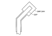
- the width of the gate wiring main body GH is gradually reduced at the end portion (inside the dotted line frame A) of the gate design pattern GDP. There are two end edges.
- the gate mask pattern GMP is a pattern in which the gate design pattern GDP is expanded outward by a predetermined distance as a whole, including its terminal portion.
- FIG. 17 shows a gate design pattern GDP of the gate wiring body GH of the semiconductor device according to the third embodiment.
- FIG. 18 shows a gate mask pattern GMP obtained by performing optical proximity effect correction on the gate design pattern GDP.
- An example is shown.
- One end side orthogonal to is arranged. That is, the terminal side corresponding to the end surface in the direction orthogonal to the direction in which the gate wiring main body extends is arranged.
- the gate design pattern GDP is a pattern that is expanded outward by a predetermined distance as a whole.
- the end portion is greatly retracted from the position corresponding to the end portion of the gate design pattern. Is suppressed.
- a pattern more faithful to the gate design pattern can be formed as the gate wiring body.
- the layout of a logic circuit constructed by combining a plurality of cells there are places where the bent second gate wiring portions are close to each other and places where they are not, depending on how the cells are arranged.
- processing for further correcting the gate design pattern data is performed so that the hammerhead pattern is physically drawn (MPD (Mask Pattern Data). Specification) processing). That is, a process of retreating a part of the patterns so that the two hammer head patterns approaching each other are separated from each other according to the approach mode.
- a gate mask pattern GMP (GHH) shown in FIG. 19 is assumed as a gate mask pattern including a standard (reference) hammerhead pattern by optical proximity effect correction.
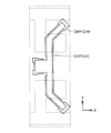
- a layout shown in FIG. 20 is assumed as an array in which cells of a plurality of inverter circuits are arranged.
- the gate mask is formed by retreating the sides facing each other from the reference gate mask pattern GMP while leaving the sides not facing each other as they are.
- the data is corrected so as to be the pattern GMP1.
- the data is corrected so that the gate mask pattern GMP2 in which the sides facing each other are retreated from the reference gate mask pattern GMP. .
- the gate mask pattern GMP (refer to FIG. 19) is used as it is as the gate mask pattern. Become a pattern.
- MPD processing By performing such processing (MPD processing), it is possible to reliably draw a gate mask pattern in which the terminal portion of the gate wiring body has a hammerhead pattern on the photomask. As a result, a gate wiring body more faithful to the gate design pattern can be formed as a logic circuit. As a result, the logic circuit can be stably operated.
- the angle ⁇ at which the second gate wiring portion GHB2 bends with respect to the first gate wiring portion GHB1 is 45 ° has been described as an example.
- the angle ⁇ is preferably 45 ° when the gate mask pattern of the gate wiring body is formed by electronic drawing.
- the angle ⁇ is not limited to 45 °, and may be in the range of 20 ° to 80 °.
- the second gate wiring portion is Y in order to secure a length extending from the element formation region to the element isolation insulating film as the second gate wiring portion. Since it approaches the axial direction, the length in the grid direction becomes disadvantageous in terms of layout.
- the second gate wiring portion GHB2 approaches the element forming region near the batting diffusion BDV (BDE)
- the region where the metal silicide film is formed is narrowed due to manufacturing variations. There is concern that the resistance will rise.
- the second gate wiring portion approaches the X-axis direction, and when the gate wiring portions of adjacent cells approach each other, the short margin disappears.
- the numerical values such as the film thickness and dimensions given in each embodiment are examples, and are not limited to these.
- the structure of the gate wiring portion parallel to the Y-axis direction and the structure of the power supply wiring and ground wiring parallel to the X-axis direction are mathematically parallel to the Y (X) axis direction. It is not intended to be a structure, but includes manufacturing errors.
- the angle formed by the second gate wiring portion with respect to the first gate wiring portion is not intended to be a mathematically exact angle, and this also naturally includes manufacturing errors.
- the semiconductor device including the gate wiring portion described above is not limited to the cell of the inverter circuit, and can be applied to a semiconductor device including a gate wiring portion that crosses the element formation region.
- the present invention can contribute to miniaturization of a semiconductor device provided with a logic circuit or the like.
- INV inverter circuit QP p-channel field effect transistor, QN n-channel field effect transistor, SUB semiconductor substrate, EB element isolation insulating film, PER element formation area, NER element formation area, NW N well, PW P well, PC p Channel region, NC n channel region, PF P + impurity region, PMS metal silicide film, NF N + impurity region, NMS metal silicide film, GHB gate wiring part, GHB1 first gate wiring part, GHB2 second gate wiring part, GHB3 third Gate wiring part, GH gate wiring main body, GZ gate insulating film, GS sidewall insulating film, GMS metal silicide film, GEP gate electrode part, GEN gate electrode part, TA tap part, NT N + impurity region, TB tap part, P P + impurity region, BDV butting diffusion, BDE butting diffusion, DF1, first interlayer insulating film, DF2, second interlayer insulating film, CH contact hole, PL plug, BM1, barrier
Landscapes
- Design And Manufacture Of Integrated Circuits (AREA)
- Semiconductor Integrated Circuits (AREA)
- Engineering & Computer Science (AREA)
- General Engineering & Computer Science (AREA)
Abstract
Description
実施の形態1では、ゲート配線部を2回屈曲させた半導体装置について説明する。図2および図3に示すように、インバータ回路のセルにおける半導体基板SUBの表面には、素子分離絶縁膜EBによって電気的に互いに絶縁された2つの素子形成領域PER,NER(活性領域)が規定されている。一方の素子形成領域PERでは、その表面から所定の深さにわたりNウェルNWが形成されている。他方の素子形成領域NERでは、その表面から所定の深さにわたりPウェルPWが形成されている。
実施の形態2では、ゲート配線部を1回屈曲させた半導体装置の第1の例について説明する。図7、図8および図9に示すように、ゲート配線部GHBは、第1ゲート電極部GEB1を含む第1ゲート配線部GHB1と、第2ゲート電極部GEB2を含む第2ゲート配線部GHB2とを備えている。
実施の形態3では、ゲート配線部を1回屈曲させた半導体装置の第2の例について説明する。
すでに述べたように、所定の寸法等をもってゲート電極部(ゲート配線部)が素子形成領域PERと素子形成領域NERとを横切るようにするためには、ゲート配線部を、素子形成領域PER(PER)から素子分離絶縁膜EB上へ向かって、所定の長さ分延在させる必要がある。ゲート配線部のパターン(形状)は、実質的にゲート配線本体のパターニングに依存する。ゲート配線本体は、たとえば、ポリシリコン膜等の上に写真製版処理によってレジストパターンを形成し、そのレジストパターンをマスクとしてポリシリコン膜等にエッチングを施すことによりパターニングされる。
Claims (7)
- 電源電位と接地電位との間に相補型スイッチング素子を直列に接続したインバータ回路を含む半導体装置であって、
主表面を有する半導体基板と、
前記半導体基板の表面上に形成され、第1の方向に平行に延在し、電源電位が印加される電源配線と、
前記半導体基板の表面上に形成され、前記電源配線に対して前記第1の方向と直交する第2の方向に距離を隔てて前記第1の方向に平行に延在し、接地電位が印加される接地配線と、
前記電源配線と前記接地配線とによって挟まれた前記半導体基板の領域において素子分離絶縁膜によってそれぞれ規定され、前記相補型スイッチング素子のための2つの素子形成領域と、
前記素子形成領域のそれぞれを横切るように形成されたゲート配線部と
を有し、
前記ゲート配線部は、
前記電源配線が配置されている側および前記接地配線が配置されている側の一方の側から他方の側へ前記第2の方向に平行に形成されて、前記素子形成領域内における所定の位置まで延在する第1ゲート配線部と、
前記第1ゲート配線部から前記他方の側へ、前記第2の方向に対して斜めに交差する第3の方向に平行に形成されて、前記素子形成領域と前記素子分離絶縁膜との境界として前記第1の方向に平行な境界を斜めに跨ぐように延在する第2ゲート配線部と
を備えた、半導体装置。 - 前記ゲート配線部は、前記第2ゲート配線部から前記他方の側へ、前記第2の方向に平行にさらに延在する第3ゲート配線部を含む、請求項1記載の半導体装置。
- 前記第2ゲート配線部は、前記他方の側へ、前記第3の方向に平行に前記素子分離絶縁膜上をさらに延在する、請求項1記載の半導体装置。
- 前記第1ゲート配線部に対して前記第2ゲート配線部のなす角度は10°~80°である、請求項1記載の半導体装置。
- 前記第1ゲート配線部に対して前記第2ゲート配線部のなす角度は45°である、請求項4記載の半導体装置。
- 前記ゲート配線部は、互いに間隔を隔てて対向する両側面を有するゲート配線本体を含み、
前記ゲート配線本体は、前記一方の側の終端部および前記他方の側の終端部として、前記両側面に直交する終端面を有する、請求項1記載の半導体装置。 - 主表面を有する半導体基板と、
前記半導体基板において、素子分離絶縁膜によって規定された素子形成領域と、
前記素子形成領域を横切るように形成されたゲート配線部と
を有し、
前記ゲート配線部は、
前記素子形成領域と前記素子分離絶縁膜との境界に向かって前記境界が延在する方向と直交する方向に形成されて、前記素子形成領域内における所定の位置まで延在する第1ゲート配線部と、
前記第1ゲート配線部から屈曲して前記境界を斜めに跨ぐように延在する第2ゲート配線部と
を備えた、半導体装置。
Priority Applications (3)
| Application Number | Priority Date | Filing Date | Title |
|---|---|---|---|
| US14/112,926 US9054103B2 (en) | 2011-04-20 | 2012-03-26 | Semiconductor device |
| JP2013510924A JP5711812B2 (ja) | 2011-04-20 | 2012-03-26 | 半導体装置 |
| US14/711,771 US20150243735A1 (en) | 2011-04-20 | 2015-05-14 | Semiconductor device |
Applications Claiming Priority (2)
| Application Number | Priority Date | Filing Date | Title |
|---|---|---|---|
| JP2011-093880 | 2011-04-20 | ||
| JP2011093880 | 2011-04-20 |
Related Child Applications (2)
| Application Number | Title | Priority Date | Filing Date |
|---|---|---|---|
| US14/112,926 A-371-Of-International US9054103B2 (en) | 2011-04-20 | 2012-03-26 | Semiconductor device |
| US14/711,771 Continuation US20150243735A1 (en) | 2011-04-20 | 2015-05-14 | Semiconductor device |
Publications (1)
| Publication Number | Publication Date |
|---|---|
| WO2012144295A1 true WO2012144295A1 (ja) | 2012-10-26 |
Family
ID=47041413
Family Applications (1)
| Application Number | Title | Priority Date | Filing Date |
|---|---|---|---|
| PCT/JP2012/057690 Ceased WO2012144295A1 (ja) | 2011-04-20 | 2012-03-26 | 半導体装置 |
Country Status (3)
| Country | Link |
|---|---|
| US (2) | US9054103B2 (ja) |
| JP (1) | JP5711812B2 (ja) |
| WO (1) | WO2012144295A1 (ja) |
Citations (5)
| Publication number | Priority date | Publication date | Assignee | Title |
|---|---|---|---|---|
| JPH02170437A (ja) * | 1988-12-22 | 1990-07-02 | Fuji Electric Co Ltd | Mis型半導体装置の製造方法 |
| JPH077143A (ja) * | 1993-01-29 | 1995-01-10 | Sgs Thomson Microelectron Inc | 二重バッファベースゲートアレイセル |
| JPH11103054A (ja) * | 1997-09-29 | 1999-04-13 | Kawasaki Steel Corp | 半導体装置 |
| JPH11330461A (ja) * | 1998-05-14 | 1999-11-30 | Nec Corp | 屈曲ゲート電極を有する半導体装置およびその製造方法 |
| JP2009032788A (ja) * | 2007-07-25 | 2009-02-12 | Renesas Technology Corp | 半導体装置 |
Family Cites Families (1)
| Publication number | Priority date | Publication date | Assignee | Title |
|---|---|---|---|---|
| JPH05198593A (ja) | 1992-01-22 | 1993-08-06 | Hitachi Ltd | パラメータ抽出方法 |
-
2012
- 2012-03-26 WO PCT/JP2012/057690 patent/WO2012144295A1/ja not_active Ceased
- 2012-03-26 JP JP2013510924A patent/JP5711812B2/ja not_active Expired - Fee Related
- 2012-03-26 US US14/112,926 patent/US9054103B2/en active Active
-
2015
- 2015-05-14 US US14/711,771 patent/US20150243735A1/en not_active Abandoned
Patent Citations (5)
| Publication number | Priority date | Publication date | Assignee | Title |
|---|---|---|---|---|
| JPH02170437A (ja) * | 1988-12-22 | 1990-07-02 | Fuji Electric Co Ltd | Mis型半導体装置の製造方法 |
| JPH077143A (ja) * | 1993-01-29 | 1995-01-10 | Sgs Thomson Microelectron Inc | 二重バッファベースゲートアレイセル |
| JPH11103054A (ja) * | 1997-09-29 | 1999-04-13 | Kawasaki Steel Corp | 半導体装置 |
| JPH11330461A (ja) * | 1998-05-14 | 1999-11-30 | Nec Corp | 屈曲ゲート電極を有する半導体装置およびその製造方法 |
| JP2009032788A (ja) * | 2007-07-25 | 2009-02-12 | Renesas Technology Corp | 半導体装置 |
Also Published As
| Publication number | Publication date |
|---|---|
| US9054103B2 (en) | 2015-06-09 |
| JP5711812B2 (ja) | 2015-05-07 |
| JPWO2012144295A1 (ja) | 2014-07-28 |
| US20150243735A1 (en) | 2015-08-27 |
| US20140043063A1 (en) | 2014-02-13 |
Similar Documents
| Publication | Publication Date | Title |
|---|---|---|
| TW202029461A (zh) | 積體電路 | |
| US20150249080A1 (en) | Method and apparatus for forming an integrated circuit with a metalized resistor in a standard cell configuration | |
| WO2012056615A1 (ja) | 半導体装置 | |
| TW201814835A (zh) | 積體電路中採用之自對準局部互連線用之方法、結構與設計 | |
| WO2018042986A1 (ja) | 半導体集積回路装置 | |
| JP2006156778A (ja) | 半導体装置及びそのレイアウト設計方法 | |
| KR102218929B1 (ko) | 브릿징 위험성 감소 및 성능 향상을 위한 상이한 비아 크기의 구성 | |
| CN102891142A (zh) | 具有无方向的去耦合电容器的半导体器件及其制造方法 | |
| KR20180015399A (ko) | 반도체 장치 및 이의 제조 방법 | |
| US8841774B2 (en) | Semiconductor device including a first wiring having a bending portion a via | |
| JP2013161878A (ja) | 半導体装置、および半導体装置の製造方法 | |
| US9000535B2 (en) | Semiconductor device and semiconductor device manufacturing method | |
| JP6094023B2 (ja) | 半導体装置の製造方法 | |
| JP5830400B2 (ja) | 半導体装置、および半導体装置の製造方法 | |
| JP6097434B2 (ja) | 半導体装置、および半導体装置の製造方法 | |
| JP2011199034A (ja) | 半導体装置 | |
| WO2018150913A1 (ja) | 半導体集積回路装置 | |
| JP5711812B2 (ja) | 半導体装置 | |
| TW201507013A (zh) | 半導體裝置之製造方法 | |
| JP3637826B2 (ja) | 半導体記憶装置 | |
| CN107706233A (zh) | 半导体元件及其制作方法 | |
| JP2011187472A (ja) | 半導体装置 | |
| JP2010010590A (ja) | 半導体装置およびその製造方法 | |
| CN103415922B (zh) | 半导体器件和半导体器件的制造方法 | |
| JP5425533B2 (ja) | 半導体集積回路装置の製造方法 |
Legal Events
| Date | Code | Title | Description |
|---|---|---|---|
| 121 | Ep: the epo has been informed by wipo that ep was designated in this application |
Ref document number: 12773948 Country of ref document: EP Kind code of ref document: A1 |
|
| ENP | Entry into the national phase |
Ref document number: 2013510924 Country of ref document: JP Kind code of ref document: A |
|
| WWE | Wipo information: entry into national phase |
Ref document number: 14112926 Country of ref document: US |
|
| NENP | Non-entry into the national phase |
Ref country code: DE |
|
| 122 | Ep: pct application non-entry in european phase |
Ref document number: 12773948 Country of ref document: EP Kind code of ref document: A1 |