WO2012141121A1 - 半導体装置 - Google Patents
半導体装置 Download PDFInfo
- Publication number
- WO2012141121A1 WO2012141121A1 PCT/JP2012/059641 JP2012059641W WO2012141121A1 WO 2012141121 A1 WO2012141121 A1 WO 2012141121A1 JP 2012059641 W JP2012059641 W JP 2012059641W WO 2012141121 A1 WO2012141121 A1 WO 2012141121A1
- Authority
- WO
- WIPO (PCT)
- Prior art keywords
- region
- active region
- sub
- semiconductor device
- threshold voltage
- Prior art date
- Legal status (The legal status is an assumption and is not a legal conclusion. Google has not performed a legal analysis and makes no representation as to the accuracy of the status listed.)
- Ceased
Links
Images
















Classifications
-
- H—ELECTRICITY
- H10—SEMICONDUCTOR DEVICES; ELECTRIC SOLID-STATE DEVICES NOT OTHERWISE PROVIDED FOR
- H10D—INORGANIC ELECTRIC SEMICONDUCTOR DEVICES
- H10D30/00—Field-effect transistors [FET]
- H10D30/60—Insulated-gate field-effect transistors [IGFET]
- H10D30/64—Double-diffused metal-oxide semiconductor [DMOS] FETs
- H10D30/66—Vertical DMOS [VDMOS] FETs
- H10D30/663—Vertical DMOS [VDMOS] FETs having both source contacts and drain contacts on the same surface, i.e. up-drain VDMOS
-
- H—ELECTRICITY
- H10—SEMICONDUCTOR DEVICES; ELECTRIC SOLID-STATE DEVICES NOT OTHERWISE PROVIDED FOR
- H10D—INORGANIC ELECTRIC SEMICONDUCTOR DEVICES
- H10D12/00—Bipolar devices controlled by the field effect, e.g. insulated-gate bipolar transistors [IGBT]
- H10D12/411—Insulated-gate bipolar transistors [IGBT]
- H10D12/441—Vertical IGBTs
- H10D12/461—Vertical IGBTs having non-planar surfaces, e.g. having trenches, recesses or pillars in the surfaces of the emitter, base or collector regions
- H10D12/481—Vertical IGBTs having non-planar surfaces, e.g. having trenches, recesses or pillars in the surfaces of the emitter, base or collector regions having gate structures on slanted surfaces, on vertical surfaces, or in grooves, e.g. trench gate IGBTs
-
- H—ELECTRICITY
- H10—SEMICONDUCTOR DEVICES; ELECTRIC SOLID-STATE DEVICES NOT OTHERWISE PROVIDED FOR
- H10D—INORGANIC ELECTRIC SEMICONDUCTOR DEVICES
- H10D30/00—Field-effect transistors [FET]
- H10D30/01—Manufacture or treatment
- H10D30/021—Manufacture or treatment of FETs having insulated gates [IGFET]
- H10D30/028—Manufacture or treatment of FETs having insulated gates [IGFET] of double-diffused metal oxide semiconductor [DMOS] FETs
- H10D30/0291—Manufacture or treatment of FETs having insulated gates [IGFET] of double-diffused metal oxide semiconductor [DMOS] FETs of vertical DMOS [VDMOS] FETs
- H10D30/0295—Manufacture or treatment of FETs having insulated gates [IGFET] of double-diffused metal oxide semiconductor [DMOS] FETs of vertical DMOS [VDMOS] FETs using recessing of the source electrodes
-
- H—ELECTRICITY
- H10—SEMICONDUCTOR DEVICES; ELECTRIC SOLID-STATE DEVICES NOT OTHERWISE PROVIDED FOR
- H10D—INORGANIC ELECTRIC SEMICONDUCTOR DEVICES
- H10D30/00—Field-effect transistors [FET]
- H10D30/01—Manufacture or treatment
- H10D30/021—Manufacture or treatment of FETs having insulated gates [IGFET]
- H10D30/028—Manufacture or treatment of FETs having insulated gates [IGFET] of double-diffused metal oxide semiconductor [DMOS] FETs
- H10D30/0291—Manufacture or treatment of FETs having insulated gates [IGFET] of double-diffused metal oxide semiconductor [DMOS] FETs of vertical DMOS [VDMOS] FETs
- H10D30/0297—Manufacture or treatment of FETs having insulated gates [IGFET] of double-diffused metal oxide semiconductor [DMOS] FETs of vertical DMOS [VDMOS] FETs using recessing of the gate electrodes, e.g. to form trench gate electrodes
-
- H—ELECTRICITY
- H10—SEMICONDUCTOR DEVICES; ELECTRIC SOLID-STATE DEVICES NOT OTHERWISE PROVIDED FOR
- H10D—INORGANIC ELECTRIC SEMICONDUCTOR DEVICES
- H10D30/00—Field-effect transistors [FET]
- H10D30/60—Insulated-gate field-effect transistors [IGFET]
- H10D30/64—Double-diffused metal-oxide semiconductor [DMOS] FETs
- H10D30/66—Vertical DMOS [VDMOS] FETs
- H10D30/668—Vertical DMOS [VDMOS] FETs having trench gate electrodes, e.g. UMOS transistors
-
- H—ELECTRICITY
- H10—SEMICONDUCTOR DEVICES; ELECTRIC SOLID-STATE DEVICES NOT OTHERWISE PROVIDED FOR
- H10D—INORGANIC ELECTRIC SEMICONDUCTOR DEVICES
- H10D62/00—Semiconductor bodies, or regions thereof, of devices having potential barriers
- H10D62/10—Shapes, relative sizes or dispositions of the regions of the semiconductor bodies; Shapes of the semiconductor bodies
- H10D62/17—Semiconductor regions connected to electrodes not carrying current to be rectified, amplified or switched, e.g. channel regions
- H10D62/393—Body regions of DMOS transistors or IGBTs
-
- H—ELECTRICITY
- H10—SEMICONDUCTOR DEVICES; ELECTRIC SOLID-STATE DEVICES NOT OTHERWISE PROVIDED FOR
- H10D—INORGANIC ELECTRIC SEMICONDUCTOR DEVICES
- H10D64/00—Electrodes of devices having potential barriers
- H10D64/20—Electrodes characterised by their shapes, relative sizes or dispositions
- H10D64/27—Electrodes not carrying the current to be rectified, amplified, oscillated or switched, e.g. gates
- H10D64/311—Gate electrodes for field-effect devices
- H10D64/411—Gate electrodes for field-effect devices for FETs
- H10D64/511—Gate electrodes for field-effect devices for FETs for IGFETs
- H10D64/514—Gate electrodes for field-effect devices for FETs for IGFETs characterised by the insulating layers
- H10D64/516—Gate electrodes for field-effect devices for FETs for IGFETs characterised by the insulating layers the thicknesses being non-uniform
-
- H—ELECTRICITY
- H10—SEMICONDUCTOR DEVICES; ELECTRIC SOLID-STATE DEVICES NOT OTHERWISE PROVIDED FOR
- H10D—INORGANIC ELECTRIC SEMICONDUCTOR DEVICES
- H10D64/00—Electrodes of devices having potential barriers
- H10D64/20—Electrodes characterised by their shapes, relative sizes or dispositions
- H10D64/27—Electrodes not carrying the current to be rectified, amplified, oscillated or switched, e.g. gates
- H10D64/311—Gate electrodes for field-effect devices
- H10D64/411—Gate electrodes for field-effect devices for FETs
- H10D64/511—Gate electrodes for field-effect devices for FETs for IGFETs
- H10D64/517—Gate electrodes for field-effect devices for FETs for IGFETs characterised by the conducting layers
- H10D64/519—Gate electrodes for field-effect devices for FETs for IGFETs characterised by the conducting layers characterised by their top-view geometrical layouts
-
- H—ELECTRICITY
- H10—SEMICONDUCTOR DEVICES; ELECTRIC SOLID-STATE DEVICES NOT OTHERWISE PROVIDED FOR
- H10D—INORGANIC ELECTRIC SEMICONDUCTOR DEVICES
- H10D84/00—Integrated devices formed in or on semiconductor substrates that comprise only semiconducting layers, e.g. on Si wafers or on GaAs-on-Si wafers
- H10D84/01—Manufacture or treatment
- H10D84/0123—Integrating together multiple components covered by H10D12/00 or H10D30/00, e.g. integrating multiple IGBTs
- H10D84/0126—Integrating together multiple components covered by H10D12/00 or H10D30/00, e.g. integrating multiple IGBTs the components including insulated gates, e.g. IGFETs
- H10D84/0165—Integrating together multiple components covered by H10D12/00 or H10D30/00, e.g. integrating multiple IGBTs the components including insulated gates, e.g. IGFETs the components including complementary IGFETs, e.g. CMOS devices
- H10D84/0191—Manufacturing their doped wells
-
- H—ELECTRICITY
- H10—SEMICONDUCTOR DEVICES; ELECTRIC SOLID-STATE DEVICES NOT OTHERWISE PROVIDED FOR
- H10D—INORGANIC ELECTRIC SEMICONDUCTOR DEVICES
- H10D84/00—Integrated devices formed in or on semiconductor substrates that comprise only semiconducting layers, e.g. on Si wafers or on GaAs-on-Si wafers
- H10D84/01—Manufacture or treatment
- H10D84/0123—Integrating together multiple components covered by H10D12/00 or H10D30/00, e.g. integrating multiple IGBTs
- H10D84/0126—Integrating together multiple components covered by H10D12/00 or H10D30/00, e.g. integrating multiple IGBTs the components including insulated gates, e.g. IGFETs
- H10D84/0165—Integrating together multiple components covered by H10D12/00 or H10D30/00, e.g. integrating multiple IGBTs the components including insulated gates, e.g. IGFETs the components including complementary IGFETs, e.g. CMOS devices
- H10D84/0195—Integrating together multiple components covered by H10D12/00 or H10D30/00, e.g. integrating multiple IGBTs the components including insulated gates, e.g. IGFETs the components including complementary IGFETs, e.g. CMOS devices the components including vertical IGFETs
-
- H—ELECTRICITY
- H10—SEMICONDUCTOR DEVICES; ELECTRIC SOLID-STATE DEVICES NOT OTHERWISE PROVIDED FOR
- H10D—INORGANIC ELECTRIC SEMICONDUCTOR DEVICES
- H10D84/00—Integrated devices formed in or on semiconductor substrates that comprise only semiconducting layers, e.g. on Si wafers or on GaAs-on-Si wafers
- H10D84/01—Manufacture or treatment
- H10D84/02—Manufacture or treatment characterised by using material-based technologies
- H10D84/03—Manufacture or treatment characterised by using material-based technologies using Group IV technology, e.g. silicon technology or silicon-carbide [SiC] technology
- H10D84/038—Manufacture or treatment characterised by using material-based technologies using Group IV technology, e.g. silicon technology or silicon-carbide [SiC] technology using silicon technology, e.g. SiGe
-
- H—ELECTRICITY
- H10—SEMICONDUCTOR DEVICES; ELECTRIC SOLID-STATE DEVICES NOT OTHERWISE PROVIDED FOR
- H10D—INORGANIC ELECTRIC SEMICONDUCTOR DEVICES
- H10D84/00—Integrated devices formed in or on semiconductor substrates that comprise only semiconducting layers, e.g. on Si wafers or on GaAs-on-Si wafers
- H10D84/101—Integrated devices comprising main components and built-in components, e.g. IGBT having built-in freewheel diode
- H10D84/141—VDMOS having built-in components
-
- H—ELECTRICITY
- H10—SEMICONDUCTOR DEVICES; ELECTRIC SOLID-STATE DEVICES NOT OTHERWISE PROVIDED FOR
- H10D—INORGANIC ELECTRIC SEMICONDUCTOR DEVICES
- H10D84/00—Integrated devices formed in or on semiconductor substrates that comprise only semiconducting layers, e.g. on Si wafers or on GaAs-on-Si wafers
- H10D84/80—Integrated devices formed in or on semiconductor substrates that comprise only semiconducting layers, e.g. on Si wafers or on GaAs-on-Si wafers characterised by the integration of at least one component covered by groups H10D12/00 or H10D30/00, e.g. integration of IGFETs
- H10D84/82—Integrated devices formed in or on semiconductor substrates that comprise only semiconducting layers, e.g. on Si wafers or on GaAs-on-Si wafers characterised by the integration of at least one component covered by groups H10D12/00 or H10D30/00, e.g. integration of IGFETs of only field-effect components
- H10D84/83—Integrated devices formed in or on semiconductor substrates that comprise only semiconducting layers, e.g. on Si wafers or on GaAs-on-Si wafers characterised by the integration of at least one component covered by groups H10D12/00 or H10D30/00, e.g. integration of IGFETs of only field-effect components of only insulated-gate FETs [IGFET]
- H10D84/85—Complementary IGFETs, e.g. CMOS
- H10D84/856—Complementary IGFETs, e.g. CMOS the complementary IGFETs having different architectures than each other, e.g. high-voltage and low-voltage CMOS
-
- H—ELECTRICITY
- H10—SEMICONDUCTOR DEVICES; ELECTRIC SOLID-STATE DEVICES NOT OTHERWISE PROVIDED FOR
- H10D—INORGANIC ELECTRIC SEMICONDUCTOR DEVICES
- H10D30/00—Field-effect transistors [FET]
- H10D30/60—Insulated-gate field-effect transistors [IGFET]
- H10D30/64—Double-diffused metal-oxide semiconductor [DMOS] FETs
- H10D30/66—Vertical DMOS [VDMOS] FETs
- H10D30/665—Vertical DMOS [VDMOS] FETs having edge termination structures
-
- H—ELECTRICITY
- H10—SEMICONDUCTOR DEVICES; ELECTRIC SOLID-STATE DEVICES NOT OTHERWISE PROVIDED FOR
- H10D—INORGANIC ELECTRIC SEMICONDUCTOR DEVICES
- H10D62/00—Semiconductor bodies, or regions thereof, of devices having potential barriers
- H10D62/10—Shapes, relative sizes or dispositions of the regions of the semiconductor bodies; Shapes of the semiconductor bodies
- H10D62/102—Constructional design considerations for preventing surface leakage or controlling electric field concentration
- H10D62/103—Constructional design considerations for preventing surface leakage or controlling electric field concentration for increasing or controlling the breakdown voltage of reverse-biased devices
- H10D62/105—Constructional design considerations for preventing surface leakage or controlling electric field concentration for increasing or controlling the breakdown voltage of reverse-biased devices by having particular doping profiles, shapes or arrangements of PN junctions; by having supplementary regions, e.g. junction termination extension [JTE]
- H10D62/106—Constructional design considerations for preventing surface leakage or controlling electric field concentration for increasing or controlling the breakdown voltage of reverse-biased devices by having particular doping profiles, shapes or arrangements of PN junctions; by having supplementary regions, e.g. junction termination extension [JTE] having supplementary regions doped oppositely to or in rectifying contact with regions of the semiconductor bodies, e.g. guard rings with PN or Schottky junctions
-
- H—ELECTRICITY
- H10—SEMICONDUCTOR DEVICES; ELECTRIC SOLID-STATE DEVICES NOT OTHERWISE PROVIDED FOR
- H10D—INORGANIC ELECTRIC SEMICONDUCTOR DEVICES
- H10D62/00—Semiconductor bodies, or regions thereof, of devices having potential barriers
- H10D62/10—Shapes, relative sizes or dispositions of the regions of the semiconductor bodies; Shapes of the semiconductor bodies
- H10D62/124—Shapes, relative sizes or dispositions of the regions of semiconductor bodies or of junctions between the regions
- H10D62/126—Top-view geometrical layouts of the regions or the junctions
- H10D62/127—Top-view geometrical layouts of the regions or the junctions of cellular field-effect devices, e.g. multicellular DMOS transistors or IGBTs
-
- H—ELECTRICITY
- H10—SEMICONDUCTOR DEVICES; ELECTRIC SOLID-STATE DEVICES NOT OTHERWISE PROVIDED FOR
- H10D—INORGANIC ELECTRIC SEMICONDUCTOR DEVICES
- H10D64/00—Electrodes of devices having potential barriers
- H10D64/20—Electrodes characterised by their shapes, relative sizes or dispositions
- H10D64/23—Electrodes carrying the current to be rectified, amplified, oscillated or switched, e.g. sources, drains, anodes or cathodes
- H10D64/251—Source or drain electrodes for field-effect devices
- H10D64/256—Source or drain electrodes for field-effect devices for lateral devices wherein the source or drain electrodes are recessed in semiconductor bodies
-
- H—ELECTRICITY
- H10—SEMICONDUCTOR DEVICES; ELECTRIC SOLID-STATE DEVICES NOT OTHERWISE PROVIDED FOR
- H10W—GENERIC PACKAGES, INTERCONNECTIONS, CONNECTORS OR OTHER CONSTRUCTIONAL DETAILS OF DEVICES COVERED BY CLASS H10
- H10W72/00—Interconnections or connectors in packages
- H10W72/071—Connecting or disconnecting
- H10W72/075—Connecting or disconnecting of bond wires
- H10W72/07551—Connecting or disconnecting of bond wires characterised by changes in properties of the bond wires during the connecting
- H10W72/07554—Connecting or disconnecting of bond wires characterised by changes in properties of the bond wires during the connecting changes in dispositions
-
- H—ELECTRICITY
- H10—SEMICONDUCTOR DEVICES; ELECTRIC SOLID-STATE DEVICES NOT OTHERWISE PROVIDED FOR
- H10W—GENERIC PACKAGES, INTERCONNECTIONS, CONNECTORS OR OTHER CONSTRUCTIONAL DETAILS OF DEVICES COVERED BY CLASS H10
- H10W72/00—Interconnections or connectors in packages
- H10W72/50—Bond wires
- H10W72/541—Dispositions of bond wires
- H10W72/5449—Dispositions of bond wires not being orthogonal to a side surface of the chip, e.g. fan-out arrangements
-
- H—ELECTRICITY
- H10—SEMICONDUCTOR DEVICES; ELECTRIC SOLID-STATE DEVICES NOT OTHERWISE PROVIDED FOR
- H10W—GENERIC PACKAGES, INTERCONNECTIONS, CONNECTORS OR OTHER CONSTRUCTIONAL DETAILS OF DEVICES COVERED BY CLASS H10
- H10W72/00—Interconnections or connectors in packages
- H10W72/50—Bond wires
- H10W72/541—Dispositions of bond wires
- H10W72/547—Dispositions of multiple bond wires
- H10W72/5475—Dispositions of multiple bond wires multiple bond wires connected to common bond pads at both ends of the wires
-
- H—ELECTRICITY
- H10—SEMICONDUCTOR DEVICES; ELECTRIC SOLID-STATE DEVICES NOT OTHERWISE PROVIDED FOR
- H10W—GENERIC PACKAGES, INTERCONNECTIONS, CONNECTORS OR OTHER CONSTRUCTIONAL DETAILS OF DEVICES COVERED BY CLASS H10
- H10W72/00—Interconnections or connectors in packages
- H10W72/50—Bond wires
- H10W72/59—Bond pads specially adapted therefor
-
- H—ELECTRICITY
- H10—SEMICONDUCTOR DEVICES; ELECTRIC SOLID-STATE DEVICES NOT OTHERWISE PROVIDED FOR
- H10W—GENERIC PACKAGES, INTERCONNECTIONS, CONNECTORS OR OTHER CONSTRUCTIONAL DETAILS OF DEVICES COVERED BY CLASS H10
- H10W72/00—Interconnections or connectors in packages
- H10W72/90—Bond pads, in general
- H10W72/921—Structures or relative sizes of bond pads
- H10W72/926—Multiple bond pads having different sizes
-
- H—ELECTRICITY
- H10—SEMICONDUCTOR DEVICES; ELECTRIC SOLID-STATE DEVICES NOT OTHERWISE PROVIDED FOR
- H10W—GENERIC PACKAGES, INTERCONNECTIONS, CONNECTORS OR OTHER CONSTRUCTIONAL DETAILS OF DEVICES COVERED BY CLASS H10
- H10W90/00—Package configurations
- H10W90/701—Package configurations characterised by the relative positions of pads or connectors relative to package parts
- H10W90/751—Package configurations characterised by the relative positions of pads or connectors relative to package parts of bond wires
- H10W90/753—Package configurations characterised by the relative positions of pads or connectors relative to package parts of bond wires between laterally-adjacent chips
-
- H—ELECTRICITY
- H10—SEMICONDUCTOR DEVICES; ELECTRIC SOLID-STATE DEVICES NOT OTHERWISE PROVIDED FOR
- H10W—GENERIC PACKAGES, INTERCONNECTIONS, CONNECTORS OR OTHER CONSTRUCTIONAL DETAILS OF DEVICES COVERED BY CLASS H10
- H10W90/00—Package configurations
- H10W90/701—Package configurations characterised by the relative positions of pads or connectors relative to package parts
- H10W90/751—Package configurations characterised by the relative positions of pads or connectors relative to package parts of bond wires
- H10W90/756—Package configurations characterised by the relative positions of pads or connectors relative to package parts of bond wires between a chip and a stacked lead frame, conducting package substrate or heat sink
Definitions
- the present invention is a semiconductor device (or a semiconductor integrated circuit effective device applied to a semiconductor device such as a power MOSFET (Metal Oxide Field Effect Transistor) or a MISFET (Metal Insulator Semiconductor).
- a semiconductor device or a semiconductor integrated circuit effective device applied to a semiconductor device such as a power MOSFET (Metal Oxide Field Effect Transistor) or a MISFET (Metal Insulator Semiconductor).
- Patent Document 1 Japanese Patent Laid-Open No. 2003-133557 (Patent Document 1) or the corresponding US Pat. No. 6,806,548 (Patent Document 2) discloses a trench gate type vertical gate used for switching a power supply circuit.
- a channel Very Channel
- SBD Schottky Barrier Diode
- a power system active element having an insulated gate such as a power MOSFET used for a power source or a power conversion device generates a jumping voltage at the time of switching.
- This jumping voltage causes noise to a power supply circuit such as a digital signal processing circuit and causes a malfunction of a logic circuit or the like.
- This problem is not limited to a single power MOSFET or the like, but an IGBT (Insulated Gate Bipolar Transistor) and CMOS (Complementary Metal Oxide Semiconductor), etc., to which these structures are applied, and these power active devices as a single unit. This is an important problem even in an integrated circuit device integrated on a chip.
- An object of the present invention is to provide a highly reliable semiconductor device.
- the active cell region has a lower threshold voltage than other regions, and the occupied area is relatively small.
- a narrow sub-active cell region is provided.
- a sub-active cell region having a threshold voltage lower than other regions and a relatively small occupation area is provided in the active cell region.
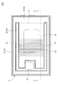
- FIG. 1 is a schematic circuit diagram showing a circuit configuration of a DC-DC converter for a computer, which is a main application field of a semiconductor device according to each embodiment of the present application. It is the whole semiconductor chip top view of power MOSFET which is an example of the semiconductor device of one embodiment of this application.
- FIG. 3 is a schematic cross-sectional view of a chip corresponding to the X-X ′ cross section of FIG. 2. It is a semiconductor chip whole upper surface schematic diagram which shows the distribution condition (single ring-shaped distribution) of the subactive area
- FIG. 5 is a partial cross-sectional view of a semiconductor chip corresponding to an A-A ′ cross section of a main and sub active region boundary peripheral cutout region R3 of FIG. 4.
- FIG. 6 is a detailed cross-sectional view of a unit cell region 20m of the main active region of FIG.
- FIG. 6 is a detailed cross-sectional view of a unit cell region 20s of the sub-active region of FIG.
- FIG. 3 is an enlarged top view of a gate electrode lead-out region R1 in FIG. 2.
- FIG. 6 is a partial cross-sectional view of a wafer during a manufacturing process (epitaxial growth process) of a part corresponding to FIG. 5.
- FIG. 5 is a partial cross-sectional view of a semiconductor chip corresponding to an A-A ′ cross section of a main and sub active region boundary peripheral cutout region R3 of FIG. 4.
- FIG. 6 is a detailed cross-sectional view of a unit cell region 20m of the main active region of FIG.
- FIG. 6 is a partial cross-sectional view of the wafer during the manufacturing process (trench formation process) of the part corresponding to FIG. 5.
- FIG. 6 is a partial cross-sectional view of a wafer during a manufacturing process (gate insulating film formation and polysilicon electrode embedding process) of a part corresponding to FIG. 5.
- FIG. 6 is a partial cross-sectional view of a wafer in the middle of a manufacturing process (a P-type body region introduction step for a main active region) corresponding to FIG. 5.
- FIG. 6 is a partial cross-sectional view of a wafer during a manufacturing process of a portion corresponding to FIG. 5 (P-type body region introduction step of a sub-active region).
- FIG. 6 is a partial cross-sectional view of the wafer in the middle of the manufacturing process of the part corresponding to FIG. 5 (metal film formation and metal source electrode patterning process).
- FIG. 6 is a partial cross-sectional view of a wafer during a manufacturing process (back grinding process) of a portion corresponding to FIG. 5.
- FIG. 6 is a partial cross-sectional view of the wafer during the manufacturing process (back surface metal electrode film forming step) of the portion corresponding to FIG. 5.
- FIG. 7 shows a subactive region corresponding to FIG. 7 relating to the first modification of the active cell structure of the power MOSFET which is an example of the semiconductor device according to the embodiment of the present application (a structure in which the gate insulating film is relatively thin in the subactive region).
- FIG. 4 It is a detailed sectional view of a unit cell region 20s.
- the active region on the upper surface of the semiconductor chip of the power MOSFET corresponding to FIG. 4 relating to the modification 4 (multiple single connection distribution) regarding the distribution of the sub-active region in the active region of the power MOSFET which is an example of the semiconductor device of the one embodiment of the present application It is a semiconductor chip whole upper surface schematic diagram which shows the distribution condition of an internal subactive region.
- the power MOSFET semiconductor chip corresponding to FIG. 4 relating to the modification 6 (the linear dispersion distribution in the gate extending direction) regarding the distribution of the sub-active region in the active region of the power MOSFET which is an example of the semiconductor device according to the embodiment of the present application.
- FIG. 31 is a schematic top view of the entire semiconductor chip showing the distribution of sub-active regions inside the active region on the top surface of the semiconductor chip of the power MOSFET corresponding to FIG. 30 (two-dimensional single-connected end concentration distribution corresponding to FIG. 26);
- FIG. 32 is a chip local enlarged top view corresponding to the gate electrode lead-out region cutout region R1 of FIGS. 30 and 31; It is a terminal arrangement diagram of an IGBT (Insulated gate Bipolar Transistor) which is an example of another active device to which the embodiments and the like described in the present application are applied.
- IGBT Insulated gate Bipolar Transistor
- FIG. 7 is a unit cell cross-sectional view of an IGBT which is an example of another active device to which the embodiments and the like described in the present application corresponding to FIG. 6 are applied.
- FIG. 2 is a chip top view layout diagram of an integrated power supply element in which main parts of the circuit elements in FIG. 1 are integrated on a single chip.
- FIG. 39 is a schematic cross-sectional view of a chip portion corresponding to the Y-Y ′ cross section of FIG. 38. It is an effect explanatory view which shows the occupancy rate dependency of the jumping voltage and power loss for demonstrating the effectiveness of the semiconductor device of each embodiment of this application of the subactive region. It is a package drawing of the semiconductor chip of power MOSFET which is an example of the semiconductor device of one embodiment of this application.
- each unit cell region has the following: (D1) a body region provided in the semiconductor substrate on the first main surface side of the drift region and having a second conductivity type opposite to the first conductivity type; (D2) a gate insulating film provided in a surface region of the semiconductor substrate on the first main surface side so as to be in contact with the body region; (D3) a gate electrode provided in the surface region of the semiconductor substrate via the gate insulating film; (D4) an interlayer insulating film provided on the gate electrode; (D5) A source region having the first conductivity type provided on the first main surface side surface of the semiconductor substrate so as to be in contact with the gate insulating film; (D7) a metal source electrode provided on
- the ratio of the second occupied area to the sum of the first occupied area and the second occupied area is 1% or more and 20% or less.
- the ratio of the second occupied area to the sum of the first occupied area and the second occupied area is 5% or more and 20% or less.
- the difference between the first threshold voltage and the second threshold voltage is caused by an impurity concentration of the body region in the main active region and the sub active region.
- the difference between the first threshold voltage and the second threshold voltage is a difference in thickness of the gate insulating film in the main active region and the sub active region. caused by.
- planar shape of the sub active region is a plurality of dot shapes.
- the sub-active region is a plurality of linear regions.
- the value of the second threshold voltage is 45% or more and 85% or less of the value of the first threshold voltage.
- the semiconductor device further includes the following: (E) a gate pad provided on the first main surface of the semiconductor substrate; (F) a first current path between the gate pad and each gate electrode in the main active region; (G) a second current path between the gate pad and each gate electrode in the sub-active region; Here, the resistance value of the second current path is larger than the resistance value of the first current path.
- the term “semiconductor device” mainly refers to various transistors (active elements) alone, or a device in which resistors, capacitors, etc. are integrated on a semiconductor chip or the like (for example, a single crystal silicon substrate).
- a MISFET Metal Insulator Semiconductor Effect Transistor
- MOSFET Metal Oxide Field Element Effect Transistor
- representative examples of various single transistors include power MOSFETs and IGBTs (Insulated Gate Bipolar Transistors). Note that power active elements such as power MOSFETs described in the present application are normally-off unless otherwise specified.
- MOS metal-oxide-semiconductor
- MIS metal-oxide-semiconductor
- the material, composition, etc. may be referred to as “X consisting of A”, etc., except when clearly stated otherwise and clearly from the context, except for A It does not exclude what makes an element one of the main components.
- the component it means “X containing A as a main component”.
- silicon member is not limited to pure silicon, but also includes SiGe alloys, other multi-component alloys containing silicon as a main component, and members containing other additives. Needless to say.
- silicon oxide film not only relatively pure undoped silicon oxide (Undoped Silicon Dioxide), but also FSG (Fluorosilicate Glass), TEOS-based silicon oxide ( Thermal oxide films such as TEOS-based silicon oxide, SiOC (Silicon Oxicarbide), carbon-doped silicon oxide, or OSG (Organosilicate glass), PSG (Phosphorus Silicate glass), BPSG (Borophosphosilicate glass), CVD Oxide film, SOG (Spin ON Glass), nano-clustering silica (Nano-Clustering Silica: NCS) coated silicon oxide, silica-based low-k insulating film (porous insulating) Needless to say, a film) and a composite film with other silicon-based insulating films including these as main constituent elements are included.
- FSG Fluorosilicate Glass
- TEOS-based silicon oxide Thermal oxide films such as TEOS-based silicon oxide, SiOC (Silicon Oxicarbide), carbon-d
- silicon nitride insulating films that are commonly used in the semiconductor field include silicon nitride insulating films.
- Materials belonging to this system include SiN, SiCN, SiNH, SiCNH, and the like.
- SiN silicon nitride
- SiNH silicon nitride
- SiCNH silicon nitride insulating films.
- SiC has similar properties to SiN, but SiON is often classified as a silicon oxide insulating film.
- “Wafer” usually refers to a single crystal silicon wafer on which a semiconductor device (same as a semiconductor integrated circuit device and an electronic device) is formed, but an insulating substrate such as an epitaxial wafer, an SOI substrate, an LCD glass substrate, and the like. Needless to say, a composite wafer such as a semiconductor layer is also included.
- the structure of the IGBT is such that a semiconductor region opposite to the drift region is interposed on the drain side of a normal vertical power MOSFET. Therefore, the gate and the source are structurally almost the same as the vertical power MOSFET, but in practice, the portion corresponding to the terminal with the bipolar transistor is called the emitter terminal. Yes.
- each element of the IGBT corresponding to the source of the vertical power MOSFET is referred to as a “source region”, “source electrode”, and “source terminal”.
- values such as “threshold voltage” when referred to as “first threshold voltage”, “second threshold voltage”, etc. mean that this is not the case, and unless otherwise stated, the average value in the target set Shall be pointed to.
- hatching or the like may be omitted even in a cross section when it becomes complicated or when it is clearly distinguished from a gap.
- the contour line of the background may be omitted even if the hole is planarly closed.
- it may be hatched to clearly indicate that it is not a void.
- Japanese Patent Application Laid-Open No. 2009-22106 (or corresponding US Patent Publication No. 2009-15224) discloses a prior patent application by the present inventors regarding a DC-DC converter used for a computer power supply or the like.
- Japanese Unexamined Patent Application Publication No. 2010-16035 (or US Patent Publication No. 2010-1790 corresponding thereto).
- FIG. 1 is a schematic circuit diagram showing a circuit configuration of a DC-DC converter for a computer, which is a main application field of the semiconductor device of each embodiment of the present application. Based on this, main application fields of the semiconductor device of each embodiment of the present application will be described.
- a power supply to a microprocessor or the like in a PC (Personal Computer) or the like is usually a constant voltage source (DC power supply Vin ) Using a VRM (Voltage Regulator Module) such as the DC-DC converter 50, for example, at a low voltage of about 1 volt (currently, for example, about 20 amperes). This amount of current may exceed 100 amperes.
- a switching signal of about 200 kHz (a typical range is about 300 kHz to about 500 kHz, and a range applied in the past and the near future is about 20 kHz to about 1 MHz) is sent from the control circuit unit 53 to the high side.
- Complementary pulse signals drive the high-side SW power MOSFET (Qhh) and the low-side SW power MOSFET (Qhl) through the driver 51 and the low-side driver 52, respectively.
- a current is supplied through the high-side SW power MOSFET (Qhh) and passes through a smoothing circuit including an output smoothing inductor 54, an output smoothing capacitor 55, and the like.
- the power supply output terminal Vdd and the ground terminal Vss are supplied to the microprocessor or the like.
- the low-side SW power MOSFET (Qhl) is a synchronous rectification switch that is turned on only when the high-side SW power MOSFET (Qhh) is off, a fast switching speed is required.
- the steep switching operation becomes a factor that increases the jumping voltage.
- the low-side SW power MOSFET (Qhl) is internally divided into a standard threshold voltage portion Qhlm that occupies most and a relatively low threshold voltage portion Qhls that occupies a relatively small portion.
- the low-side SW power MOSFET (Qhl) alleviates the steep rise when turning on, and suppresses the jumping voltage.
- FIG. 38 shows an example of the chip arrangement and wire bonding arrangement of the package configuration example of the actual semiconductor device of the circuit shown in FIG.
- This package configuration example is an embodiment adopting a QFN (Quad Flat Non-leaded package) package which is one of non-lead surface mount packages.
- QFN Quad Flat Non-leaded package
- the package tabs (die pads) 115, 116, 117 are divided into three, and the high side MOSFET (102) is provided with a source pad 118 and a gate pad 119, and a corresponding bonding pad BP of the driver IC (106). Are connected via wires 107 and 108, respectively.
- the low-side MOSFET (103) is connected via a wire 123 and a tab.
- the low-side MOSFET (103) is provided with source pads 120 and 122 and a gate pad 121, and is connected to the driver IC (106) via wirings 109 and 110 using wires, respectively. Further, it is connected to the power ground terminal 127 via a wire 124.
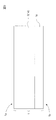
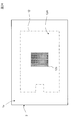
- FIG. 2 is an overall top view of a semiconductor chip of a power MOSFET which is an example of a semiconductor device according to each embodiment of the present application.
- FIG. 3 is a chip schematic cross-sectional view corresponding to the X-X ′ cross section of FIG. 2.
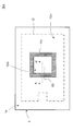
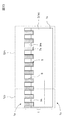
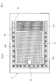
- FIG. 4 is a schematic top view of the entire semiconductor chip showing the distribution of sub-active regions (single ring distribution) inside the active region on the top surface of the semiconductor chip of the power MOSFET that is an example of the semiconductor device according to the embodiment of the present application. is there.
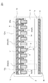
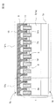
- FIG. 5 is a partial cross-sectional view of the semiconductor chip corresponding to the A-A ′ cross section of the main and sub active region boundary peripheral cutout region R 3 of FIG. FIG.
- FIG. 6 is a detailed sectional view of the unit cell region 20m of the main active region of FIG.
- FIG. 7 is a detailed cross-sectional view of the unit cell region 20s of the sub-active region of FIG.
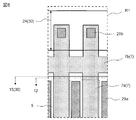
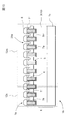
- FIG. 8 is an enlarged top view of the gate electrode lead-out region cutout region R1 of FIG. Based on these, the outline of the structure of the semiconductor chip of the semiconductor device of each embodiment of the present application will be described.
- a ring-shaped guard ring 27 (for example, an aluminum-based metal) that circulates the end is provided at the peripheral end of the semiconductor chip 2 (for example, the chip size is about 3 mm in length and about 5 mm in width).
- the electrode film 30 is composed of the same layer as the electrode film 30, and almost all of the inner part of the gate film part 24 and the metal source electrode 15 (these are also the same as the aluminum metal electrode film 30, for example) Is composed of one layer).
- a part of the gate wiring portion 24 is a gate pad portion 25 for attaching a bonding wire or the like, and the vicinity of the center of the metal source electrode 15 is similarly a source pad portion 26 for attaching a bonding wire or the like.
- a planar band-shaped unit cell region 20 (the repetition cycle of the unit cell, that is, the width of the unit cell is, for example, 0.4 micron).
- a gate polysilicon film (that is, the gate electrode 7) is embedded in the linear trench 5 in the active region 12 (active cell region).
- FIG. 3 shows an X-X ′ cross section of FIG.
- the lower half of the semiconductor chip 2 is, for example, a relatively high concentration N-type semiconductor substrate region 1s (for example, an N-type single crystal silicon substrate), and the surface of the N-type semiconductor substrate region 1s.
- N-type semiconductor substrate region 1s for example, an N-type single crystal silicon substrate
- an N-epitaxial region 1e having a thickness corresponding to the required breakdown voltage is provided, and its main part corresponds to the N-drift region 3 is doing.
- the peripheral portion of the semiconductor chip 2 is mainly an edge termination region 28, and the active region 12 is almost occupied by the internal region of the semiconductor chip 2, and the active region 12 has a strip shape (three-dimensional) in plan view. Specifically, a unit cell region 20 (width, that is, a repetition period is, for example, about 400 nm) of a rectangular parallelepiped is spread.
- the active region 12 is provided with a sub-active region 12s whose threshold voltage is set lower than other regions, that is, the main active region 12m.
- the shape is a ring shape.
- FIG. 5 shows a chip local cross-sectional view corresponding to the A-A ′ cross section of the main and sub active region boundary peripheral cutout region R 3 in FIG.
- a back surface metal electrode 4 drain electrode
- a P-type body region 9 is provided in the surface region of the N ⁇ drift region 3 on the (first main surface) side.
- a large number of trenches 5 penetrating the P-type body region 9 are provided on the semiconductor surface of the chip 2, and a trench gate electrode 7 a is embedded in each trench 5 via a gate insulating film 6. .
- An N-type source region 11 is provided in the semiconductor surface between the trenches 5, and a P-type body contact region 14 is provided in the semiconductor region at the lower end portion of the source contact portion 29a.
- An interlayer insulating film 8 such as a silicon oxide insulating film is provided on the semiconductor surface on the surface 1a (first main surface) side of the chip 2, and an electrode film such as a metal source electrode 15 is provided thereon. And is electrically connected to the P-type body contact region 14 and the N-type source region 11 through the source contact portion 29a and the like.
- the active region 12 includes the main active region 12m and the sub active region 12s.
- the threshold voltages are made different by changing the impurity concentration of each. That is, the impurity concentration of the P-type body region 9s of the sub-active region 12s is set relatively low. Therefore, the structure of the unit cell region 20 (device structure including the impurity concentration) is different between the unit cell region 20m of the main active region 12m and the unit cell region 20s of the sub active region 12s.
- FIG. 6 shows a detailed cross-sectional structure of the unit cell region 20m of the main active region 12m of FIG.
- a back surface metal electrode 4 for example, a drain electrode
- a P-type body region 9m (9) (having the second conductivity type) is provided on the surface 1a side of the N ⁇ drift region 3, and the semiconductor surface region on the surface 1a side of the N ⁇ drift region 3 is provided in the semiconductor surface region.
- Source region 11 and P-type body contact region 14 are provided.
- a trench 5 is provided from the surface 1a (first main surface) side of the semiconductor substrate 2 so as to penetrate the P-type body region 9 and reach the N ⁇ drift region 3.
- a trench gate electrode 7a such as polysilicon is embedded through the insulating film 6.
- An interlayer insulating film 8 is provided on the surface 1a of the semiconductor substrate 2, and a metal source electrode 15 composed of an aluminum-based metal film or the like is provided on the interlayer insulating film 8, via a source contact portion 29a. The source region 11 and the P-type body contact region 14 are electrically connected.
- FIG. 7 shows a detailed cross-sectional structure of the unit cell region 20s of the sub-active region 12s of FIG.
- the geometric structure is the same as in FIG. 6, but the device structure including the impurity concentration is the unit cell region 20m of the main active region 12m and the unit cell region 20s of the sub active region 12s. Is different. That is, the impurity concentration of the P-type body region 9s of the sub-active region 12s is set lower than the impurity concentration of the P-type body region 9m of the unit cell region 20m of the main active region 12m.
- FIG. 8 shows a detailed plan structure of the gate electrode lead-out region R1 shown in FIG. 2 (the same applies to the main active region 12m and the sub active region 12s).
- the gate polysilicon film 7 constituting the trench gate electrode 7a constitutes a gate lead-out polysilicon wiring portion 7b outside the trench 5, and a metal is formed in the gate contact portion 29b. It is electrically connected to the gate wiring portion 24 (a part of the aluminum-based metal electrode film 30).
- FIG. 9 is a partial cross-sectional view of the wafer during the manufacturing process (epitaxial growth process) of the part corresponding to FIG.
- FIG. 10 is a partial cross-sectional view of the wafer during the manufacturing process (trench formation process) of the part corresponding to FIG.
- FIG. 11 is a partial cross-sectional view of the wafer in the middle of the manufacturing process of the part corresponding to FIG. 5 (gate insulating film formation and polysilicon electrode embedding process).
- FIG. 12 is a partial cross-sectional view of the wafer during the manufacturing process of the portion corresponding to FIG. 5 (P-type body region introduction step of the main active region).
- FIG. 13 is a partial cross-sectional view of the wafer during the manufacturing process of the part corresponding to FIG. FIG.
- FIG. 14 is a partial cross-sectional view of the wafer in the middle of the manufacturing process (N-type source region introduction process) of the part corresponding to FIG.
- FIG. 15 is a partial cross-sectional view of the wafer in the middle of the manufacturing process (interlayer insulating film formation and contact hole formation process) of the part corresponding to FIG.
- FIG. 16 is a partial cross-sectional view of the wafer during the manufacturing process (contact hole extending process) of the part corresponding to FIG.
- FIG. 17 is a partial cross-sectional view of the wafer in the middle of the manufacturing process (P-type body contact region introduction process) corresponding to FIG.
- FIG. 18 is a partial cross-sectional view of the wafer in the middle of the manufacturing process of the part corresponding to FIG.
- a 200 ⁇ N-type silicon single crystal wafer 1s with a plane orientation of (100) 300 phi, 450 phi, or other diameter wafer may be used as required.
- the resistivity is, for example, 1 9 to 2 m ⁇ ⁇ cm), depending on the required breakdown voltage (here, the source-drain breakdown voltage is about 30 volts as an example), as shown in FIG.
- N type for example, phosphorus doping
- a silicon oxide film having a thickness of, for example, about 450 nm is formed on almost the entire device surface 1a of the wafer 1 by, eg, low pressure CVD (Chemical Vapor Deposition).
- the silicon oxide film is patterned by, for example, ordinary lithography to form a trench processing hard mask film 10.
- the trench processing hard mask film 10 is used for anisotropic dry etching (the etching atmosphere is, for example, a halogen-based gas atmosphere such as HBr).
- a trench 5 of about 15 micrometers) is formed.
- a gate oxide film 6 (gate insulating film) of, eg, about 40 nm is formed by thermal oxidation or the like.
- the gate polysilicon film 7 (for example, the thickness is formed by CVD (Chemical Vapor Deposition), for example, so as to cover almost the entire surface of the semiconductor wafer 1 on the gate oxide film 6 on the surface 1a side and fill the trench 5. About 500 nm).
- the gate polysilicon film 7 is etched back by dry etching using an etching gas such as SF 6 . Thereby, the trench gate electrode 7a is formed.
- the configuration of the gate insulating film 6 may be a thermal oxide film (silicon oxide film by thermal oxidation), a silicon oxide insulating film by CVD, or the like. Further, a part of the whole (a portion in contact with the silicon substrate) is a thermal oxide film (for example, a thickness of about 15 nm), and the remaining portion (a portion not in contact with the silicon substrate) is a silicon oxide insulating film or the like by CVD or the like (for example, , About 25 nm thick).
- a P-type body region 9m of the main active region 12m is introduced. That is, for example, the P-type body region 9m (P-type well region or channel region) is introduced by ion implantation from the device surface 1a side of the wafer 1 in a state where the sub-active region 12s is covered with a resist film or the like.
- the ion implantation conditions for example, ion species: boron, implantation energy: about 200 keV, concentration: about 7 ⁇ 10 12 / cm 2 can be exemplified as preferable ones. Thereafter, the resist film that has become unnecessary is removed by ashing or the like.
- a P-type body region 9s of the sub-active region 12s is introduced. That is, for example, a P-type body region 9s (P-type well region or channel region) is introduced by ion implantation from the device surface 1a side of the wafer 1 with the main active region 12m or the like covered with a resist film or the like.
- ion implantation conditions for example, ion species: boron, implantation energy: about 200 keV, concentration: about 2 ⁇ 10 12 / cm 2 can be exemplified as preferable ones. Thereafter, the resist film that has become unnecessary is removed by ashing or the like.
- the N-type source region 11 is introduced by ion implantation from the device surface 1 a side of the wafer 1.
- ion implantation conditions for example, ion species: arsenic, implantation energy: about 45 keV, concentration: about 3 ⁇ 10 15 / cm 2 can be exemplified as preferable ones.
- an interlayer insulating film 8 is formed on almost the entire device surface 1a of the wafer 1 by, for example, CVD.
- an insulating film made of a PSG (Phospho-Silicate Glass) film for example, a thickness of about 300 nm
- an etching mask pattern such as a resist film is formed on the device surface 1a of the wafer 1 by ordinary lithography, and anisotropic dry etching is performed using the resist mask pattern as a mask to form the source contact portion 29a (contact A hole or contact groove) is opened.
- the contact groove 29a is extended deeper than the source region 11 by anisotropic dry etching (the etching amount is about 200 nm, for example).
- a P-type body is formed in the surface region of the semiconductor substrate in a self-aligned manner by, for example, ion-implanting P-type impurities into almost the entire surface from the surface 1a side of the semiconductor wafer 1.
- Contact region 14 P-type high-concentration contact impurity region
- ion species for example, ion species: BF 2 , implantation energy: about 30 keV, and concentration: about 1 ⁇ 10 15 / cm 2 can be exemplified as preferable ones.
- a TiW film having a thickness of, for example, about 300 nm (a large portion of titanium in the TiW film is formed by sputtering film formation, for example, on almost the entire surface of the semiconductor wafer 1 on the surface 1a side. Subsequent heat treatment moves to the silicon interface to form silicide and contributes to improving contact characteristics, but these processes are complicated and are not shown in the drawing).
- an aluminum-based metal film having a thickness of, for example, about 3 ⁇ m to 5 ⁇ m (several percent silicon) is formed on almost the entire surface of the semiconductor wafer 1 on the TiW film on the surface 1a side by, for example, sputtering. Etc. to which aluminum is added).
- the TiW film and the aluminum metal film constitute an aluminum metal electrode film 30. Thereafter, by patterning the aluminum-based metal electrode film 30 by normal lithography, as shown in FIG. 2, the metal source electrode 15, the gate wiring portion 24, the guard ring 27, and the like are formed. If necessary, subsequently, as a final passivation film, for example, an organic film containing polyimide as a main component (for example, about 2.5 micrometers in thickness) or the like is applied to almost the entire device surface 1a of the wafer 1. . Further, the final passivation film in portions such as the source pad opening 26 and the gate pad opening 25 in FIG. 2 is removed by ordinary lithography.
- a final passivation film for example, an organic film containing polyimide as a main component (for example, about 2.5 micrometers in thickness) or the like is applied to almost the entire device surface 1a of the wafer 1. .
- a wafer thickness of about 500 to 900 micrometers is required, for example, about 30 to 300 micrometers. Thin film.
- a back electrode 4 for example, a titanium film / nickel film / gold film from the side closer to the wafer
- the wafer 1 is divided into individual chips 2 (FIG. 2) by dicing or the like.
- FIG. 21 shows a sub-corresponding to FIG. 7 relating to Modification 1 (a structure in which the gate insulating film is relatively thin in the sub-active region) of the active cell structure of the power MOSFET which is an example of the semiconductor device according to the embodiment of the present application. It is a detailed sectional view of a unit cell region 20s of an active region. Based on this, a first modification of the active cell structure of the power MOSFET which is an example of the semiconductor device according to the embodiment of the present application (a structure in which the gate insulating film is relatively thin in the sub-active region) will be described.
- the geometric structure is the same, and the threshold voltage of the sub-active region 12s is changed to the main active region by making the impurity concentration of the P-type body region 9 different between the main active region 12m and the sub-active region 12s.
- the threshold voltage is set lower than the threshold voltage of the region 12m, in this example, the impurity concentrations of the P-type body regions 9m and 9s are the same, and the thickness of the gate insulating film 6 of the sub-active region 12s is relative.
- the threshold voltage is set low by reducing the thickness (for example, a thermal oxide film having a thickness of about 20 nm) (the gate insulating film 6 in the sub-active region 12s is a relatively thin gate insulating film 6t).
- the configuration of the gate insulating film 6t may be a thermal oxide film (silicon oxide film by thermal oxidation), a silicon oxide insulating film by CVD, or the like. Further, a part of the whole (part in contact with the silicon substrate) is a thermal oxide film (for example, a thickness of about 10 nm), and the remaining part (part not in contact with the silicon substrate) is a silicon oxide insulating film or the like by CVD or the like (for example, Or a laminated film having a thickness of about 10 nm).
- both the impurity concentration of the P-type body region 9 and the thickness of the gate insulating film 6 can be made different. However, the process is complicated accordingly.
- the thickness of the gate insulating film may be varied to vary the equivalent thickness of the silicon oxide film with respect to the thermal oxide film (silicon oxide film). That is, the threshold voltage may be varied by changing the material of the gate insulating film 6 or a part thereof between the main active region 12m and the sub active region 12s.
- FIG. 22 is a top view of a semiconductor chip of a power MOSFET corresponding to FIG. 4 relating to Modification 1 (multiple ring-shaped distribution) relating to the distribution of sub-active regions in the active region of the power MOSFET which is an example of the semiconductor device according to the embodiment of the present application.
- FIG. 2 is a schematic top view of the entire semiconductor chip showing the distribution of sub-active areas inside the active area in FIG.
- FIG. 23 is a top view of the semiconductor chip of the power MOSFET corresponding to FIG. 4 relating to Modification 2 (dot dispersion distribution) relating to the distribution of the sub-active region in the active region of the power MOSFET which is an example of the semiconductor device according to the embodiment of the present application.
- FIG. 1 multiple ring-shaped distribution
- FIG. 2 is a schematic top view of the entire semiconductor chip showing the distribution of sub-active areas inside the active area in FIG.
- FIG. 23 is a top view of the semiconductor chip of the power MOSFET corresponding to FIG
- FIG. 2 is a schematic top view of the entire semiconductor chip showing the distribution of sub-active areas inside the active area in FIG.
- FIG. 24 is a power MOSFET semiconductor corresponding to FIG. 4 relating to the modification 3 (two-dimensional single-connection concentrated distribution) regarding the distribution of the sub-active region in the active region of the power MOSFET which is an example of the semiconductor device according to the embodiment of the present application. It is a semiconductor chip whole upper surface schematic diagram which shows the distribution condition of the subactive area
- FIG. 25 is a top view of the semiconductor chip of the power MOSFET corresponding to FIG.
- FIG. 2 is a schematic top view of the entire semiconductor chip showing the distribution of sub-active areas inside the active area in FIG.
- FIG. 26 is a power MOSFET corresponding to FIG. 4 relating to the modification 5 (two-dimensional single connection end concentration distribution) regarding the distribution of the sub-active region in the active region of the power MOSFET which is an example of the semiconductor device according to the embodiment of the present application.
- It is a semiconductor chip whole upper surface schematic diagram which shows the distribution condition of the subactive area
- FIG. 27 is a power MOSFET corresponding to FIG. 4 relating to the modification 6 (linear extension distribution in the gate extending direction) regarding the distribution of the sub-active region in the active region of the power MOSFET which is an example of the semiconductor device according to the embodiment of the present application. It is a semiconductor chip whole upper surface schematic diagram which shows the distribution condition of the subactive area
- FIG. 28 is a diagram of a power MOSFET corresponding to FIG. 4 relating to Modification 6 (linear distribution distribution in the direction perpendicular to the gate) regarding the distribution of the sub-active region in the active region of the power MOSFET which is an example of the semiconductor device according to the embodiment of the present application.
- FIG. 22 The layout shown in FIG. 22 is obtained by dividing the ring-shaped sub-active region 12s of FIG. 4 into a plurality of ring-shaped regions. This has the merit that the temperature distribution of the entire active region 12 can be made relatively uniform, like the single ring-shaped sub-active region 12s. That is, the portion corresponding to the sub-active region 12s is on for a long time, so the amount of heat generated is larger than the other portions.
- the number of rings is not limited to two, but may be three or more.
- Dot distribution (mainly FIG. 23):
- the layout shown in FIG. 23 is a layout in which a large number of dot-like sub-active regions 12s having a relatively small area are dispersed. This layout has an advantage that the temperature distribution of the entire active region 12 can be made more uniform.
- FIG. 25 The layout shown in FIG. 25 is obtained by dividing the sub-active region 12s, which is a two-dimensional single connection region, into two in the example of FIG.
- the number of two-dimensional single connected regions is not limited to two, but may be three or more.
- the advantage of this layout is that the boundary between both regions can be arranged on the trench gate electrode 7 substantially. That is, there is an advantage that the boundary line between both regions does not pass through the channel region or the source region.
- Gate-direction linear dispersion distribution (mainly FIG. 27): In the layout shown in FIG. 27, a large number of linear regions parallel to the extending direction of the trench gate 7 are dispersed to form sub-active regions 12s.
- the merit of this layout is that, in addition to uniform temperature, the boundary between both regions can be arranged on the trench gate electrode 7 substantially. That is, there is an advantage that the boundary line between both regions does not pass through the channel region or the source region.
- the number of trenches of a single chip that is, the number of cells is around 10,000 (preferably, about several thousand to several tens of thousands).
- the single element is, for example, a bundle of adjacent cells of about 100 (preferably about several tens to several hundreds).
- Linear dispersion distribution in the gate orthogonal direction (mainly FIG. 28):
- the layout shown in FIG. 28 is obtained by rotating the layout of FIG. 27 by 90 degrees.
- This layout has a merit that it is a relatively simple layout and that the temperature distribution of the entire active region 12 can be made uniform.
- FIG. 29 is a schematic circuit diagram showing a circuit configuration of a DC-DC converter for a computer corresponding to FIG. 1 for explaining a modification of the whole chip structure of the power MOSFET which is an example of the semiconductor device according to the embodiment of the present application.
- FIG. 30 is a top view of the entire semiconductor chip of the power MOSFET corresponding to FIG. 2 relating to the low-side SW power MOSFET (Qhl) of FIG. 31 is a schematic top view of the entire semiconductor chip showing the distribution of sub-active regions inside the active region on the top surface of the semiconductor chip of the power MOSFET corresponding to FIG. 30 (two-dimensional single connection end concentration distribution corresponding to FIG. 26). .
- the low-side SW power MOSFET (Qhl) is divided into a part Qhlm corresponding to the main active region 12m and a part Qhls corresponding to the sub active region 12s in terms of circuit. ing.
- An additional resistor PR is inserted into the gate electrode (gate terminal) of the portion Qhls corresponding to the sub-active region 12s (other circuit configuration is exactly the same as that of FIG. 1). . That is, each of the gate pad 25 and the sub active region 12s is compared with the first current path P1 between the gate pad 25 and each gate electrode of the main active region 12m (the gate electrode of the portion Qhlm corresponding to the main active region).
- the resistance value of the second current path P2 (for example, (About 5 to 20 ⁇ ) is larger than the resistance value of the first current path P1 (for example, about 1 to 2 ⁇ ).
- the gate resistance of the portion Qhls corresponding to the sub-active region is higher than the gate resistance of the portion Qhlm corresponding to the main active region.
- the gate of the partial Qhls corresponding to the sub-active region 12s in the low-side SW power MOSFET (Qhl) becomes unstable together with the original low threshold voltage. That is, when the high-side SW power MOSFET (Qhh) is turned on, the portion Qhls corresponding to the sub-active region 12s in the low-side SW power MOSFET (Qhl) is self-turned on, so that the low-side SW power MOSFET (Qhl) is partially Since the low-side SW power MOSFET (Qhl) is turned on as a whole, the drain voltage can be prevented from jumping up.
- the gate terminal as the external terminal of the low-side SW power MOSFET (Qhl) is single, and the gate branches in the inside. This is advantageous in that it can be handled as a normal power MOSFET from the outside.
- the external gate terminal can actually be divided into two. In that case, an additional resistor PR can be installed outside.
- FIG. 31 shows a layout of main elements on the chip upper surface such as the main active region 12m and the sub active region 12s on the chip upper surface corresponding to FIG.
- the active region 12 is divided into a main active region 12 m and a sub active region 12 s, and the sub active region 12 s is active on the side opposite to the gate pad portion 25.
- a two-dimensional single connected region (rectangular region) occupying the region 12 is formed, and the remaining two-dimensional single connected region is the main active region 12m.
- the metal gate wiring portion 24 has a U-shape along the three sides of the active region 12, and a gate lead-out polysilicon wiring portion 7b (shown here) having a similar shape is formed below the metal gate wiring portion 24.
- the metal gate wiring portion 24 and the gate lead-out polysilicon wiring portion 7b are mutually connected in a number of gate contact portions 29b in a portion close to the main active region 12m. Are connected to each other, but are not connected to each other in the vicinity of the sub-active region 12s.
- FIG. 32 shows an enlarged plan view of the gate electrode lead-out region R1 in FIG. 30 and FIG.
- the additional resistance portion 34 substantially corresponds to (or forms part of) the additional resistance component PR of FIG.
- a desired resistance value may be obtained by, for example, narrowing the width of the doped polysilicon film as in this example.
- High resistance may be formed by ion implantation of a type impurity. In that case, the area occupied by the additional resistance portion 34 can be reduced.
- the gate polysilicon film 7 is formed not by the doped polysilicon film but by the non-doped polysilicon film and the resistance value is controlled later by ion implantation, only the additional resistance portion 34 may be reduced in implantation concentration.
- the low threshold voltage region and the destabilization of part of the gates by gate division are used together, but the threshold voltage of the sub active region 12s may be the same as that of the main active region 12m. In that case, there is an advantage that the process can be simplified.
- FIG. 33 is a terminal arrangement diagram of an IGBT which is an example of another active device to which the embodiments and the like described in the present application are applied.
- FIG. 34 is a unit cell cross-sectional view of an IGBT which is an example of another active device to which the embodiments and the like described in the present application corresponding to FIG. 6 are applied.
- FIG. 35 is a chip top surface layout diagram of an integrated power supply element in which main parts of the circuit elements in FIG. 1 are integrated on a single chip.
- 36 is a chip partial schematic cross-sectional view corresponding to the Y-Y ′ cross section of FIG. 35. Based on these, application to other active devices such as each embodiment described in the present application will be described.
- each terminal of the IGBT is normally referred to as a circuit name in a pin-corresponding relationship with the bipolar transistor.
- the terminal corresponding to the base is the gate terminal G
- the terminal corresponding to the emitter is the emitter terminal E
- the collector is the collector terminal C.
- the emitter terminal E is called the source terminal as a structural name.
- the IGBT is between the back surface 1b side of the N-type semiconductor substrate region 1s of the same portion R2 and the back surface metal electrode 4 (collector electrode) structurally identical to the power MOSFET described in FIG.
- the P-type collector region 18 is inserted. Therefore, in the structural name, the source system portion, that is, the source region 11, the N-type substrate source region 11a, the poly-Si source region 11b, the metal source electrode 15, the source pad portion 26, the source contact portion 29a, etc. Can be used. Since the gate system part corresponds as it is, it can be used as it is.
- FIG. 35 shows an example of an upper surface layout of the chip 2 of a one-chip DC-DC converter (corresponding to FIG. 1) for a personal computer, which is an example of an integrated power system device.
- the device surface 1a of the chip 2 has a high side SW power MOSFET (Qhh), a low side SW power MOSFET (Qhl), a high side driver 51 for driving the high side SW power MOSFET (Qhh), and a low side.
- a low side driver 52 for driving the SW power MOSFET (Qhl), a control circuit unit 53 for controlling the high side driver 51 and the low side driver 52 (for example, the circuit has a CMOS circuit configuration), etc. are laid out.
- the high-side SW power MOSFET (Qhh) is specifically one of the power system active elements (insulated gate type power system active elements) described in FIG. 6, FIG. 7, FIG. 21, FIG. is there.
- the low-side SW power MOSFET (Qhl) can also be composed of any of these.
- the one-chip type DC-DC converter is made on a P-type semiconductor substrate 1p, for example. That is, for example, an N-epitaxial region 1e is provided on the surface 1a (first main surface or device surface) side of the P-type semiconductor substrate 1p (P-type semiconductor substrate region) by epitaxial growth or the like. An N + buried region 19 is provided near the boundary between the epitaxial region 1e and the P-type semiconductor substrate region 1p.
- a P + element isolation region 22 is provided in the N ⁇ epitaxial region 1e such as between the CMOS region Rc and the power MOS region Rh, and a field insulating film 23 (LOCOS type or STI type insulating film) is provided.
- an N + drain extraction region 21 for extracting a drain or the like to the upper surface 1a of the chip 2 is provided, and a semiconductor on the upper surface 1a of the chip 2 is provided.
- a trench 5, a gate insulating film 6, a P-type body region 9, a source region 11, a P-type body contact region 14 and the like are provided.
- a P-well region 31p and an N-well region 31n are provided below the surface of the N-epitaxial region 1e on the top surface 1a side of the chip 2.
- a P-type source / drain region 32 is provided.
- a gate electrode 33 constituting an N-channel MOSFET (Qn) and a P-channel MOSFET (Qp) is provided. ing.
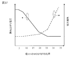
- FIG. 37 is an effect explanatory diagram showing the occupancy ratio dependency of the jumping voltage and the power loss for explaining the effectiveness of the semiconductor device of each embodiment of the present application in the sub-active region. Based on this, a general consideration of the present application and a supplementary explanation regarding each embodiment will be given.
- each embodiment described so far is based on the consideration as shown in FIG. That is, generally, the relationship between the power loss and the jumping voltage of a power system active element (low-side SW power MOSFET) such as a power MOSFET in a DC-DC converter or the like is a trade-off relationship.
- a power system active element low-side SW power MOSFET
- FIG. 37 for example, if a portion having a low threshold voltage is provided in a part of the power MOSFET (relatively narrow region compared to the whole), the power loss does not increase so much. It can be seen that there is a portion where a relatively large improvement can be obtained with respect to the jumping voltage.
- a part of the power MOSFET (a part of the whole cell, or at least a part of the part of the cell) is compared with the other part to make it easy to turn on.
- the idea is to reduce the jumping voltage caused by a steep rise in exchange for power loss.
- One way to achieve this is to create a low threshold voltage part of the low-side SW power MOSFET (Qhl) as described in Sections 2 to 5. In this way, when the low-side SW power MOSFET (Qhl) is turned on, first, the portion with the lower threshold voltage is turned on first, and then the main portion is turned on. Is reduced.
- the threshold voltage (second threshold voltage) of the portion Qhls corresponding to the sub-active region based on the threshold voltage (first threshold voltage) of the portion Qhlm corresponding to the main active region of the low-side SW power MOSFET (Qhl). ) Is generally 45% or more and 85% or less of the reference value. Further, when it is necessary to further reduce the loss, the preferable range of the threshold voltage is 55% or more and 75% or less of the reference value.
- a suitable range (area ratio) of the area ratio of the sub-active area 12s based on the area of the entire active area 12 is 1% or more and 20% or less. This is because power loss increases rapidly when the area ratio exceeds 20%.
- the preferable range of this ratio is 5% or more and 20% or less.
- the power loss rate is estimated to be about 1 to 3%.
- SBD built-in method As a method for reducing the jump voltage, a method of incorporating SBD in the chip of the low-side SW power MOSFET (Qhl) (SBD built-in method) is known, but the SBD built-in method suppresses self turn-on and jump voltage. However, there is a demerit that greatly increases the chip area.
- the present invention does not exclude the combined use of each embodiment of the present invention and the SBD built-in method.
- the N channel device is mainly formed on the upper surface of the N epitaxial layer on the N + silicon single crystal substrate.
- the present invention is not limited thereto, and P + silicon A P channel device may be formed on the upper surface of the N epitaxial layer on the single crystal substrate.
- the power MOSFET has been specifically described as an example.
- the present invention is not limited thereto, and it is needless to say that the present invention can be applied to a bipolar transistor (including IGBT). Needless to say, the present invention can also be applied to a semiconductor integrated circuit device incorporating such power MOSFETs, bipolar transistors, and the like.
- the present invention is not limited thereto, and a GaAs-based semiconductor substrate, a silicon carbide-based semiconductor substrate, and a silicon nitride. Needless to say, the present invention can be applied almost as it is to a device made on a ride-type semiconductor substrate.
- the gate electrode or the like that uses a polysilicon film has been specifically described.
- the present invention is not limited thereto, and may be a polycide film, a silicide film, or the like. Needless to say.
- the metal electrode and the aluminum-based metal film as the main constituent film have been specifically described.
- the present invention is not limited thereto, and titanium, tungsten, and the like are used. Needless to say, the present invention can also be applied to a film using a refractory metal film or a gold film as a main component film of a metal electrode.
- the drift region constituted by a single conductivity type region has been specifically described.
- the present invention is not limited to this, and a superconducting region in which the opposite conductivity type regions are alternately replaced is described. Needless to say, the present invention can also be applied to one having a super-junction type drift region.
- the present invention can be widely applied to a device structure in a semiconductor device (or a semiconductor integrated circuit device) such as a power MOSFET or a MISFET.
Landscapes
- Metal-Oxide And Bipolar Metal-Oxide Semiconductor Integrated Circuits (AREA)
- Dc-Dc Converters (AREA)
Abstract
電源または電力変換機器等に使用されるパワーMOSFET等の絶縁ゲートを有するパワー系能動素子は、スイッチングの際に跳ね上がり電圧が発生する。この跳ね上がり電圧は、ディジタル信号処理回路等の被電源供給回路へのノイズとなり、論理回路等の誤動作の原因になる等の問題がある。 本願発明は、パワーMOSFET等の絶縁ゲートを有するパワー系能動素子を有する半導体装置に於いて、アクティブセル領域に他の領域よりも閾値電圧が低く、且つ、占有面積が比較的狭い副アクティブセル領域を設けるものである。
Description
本発明は、パワーMOSFET(Metal Oxide Semiconductor Field Effect Transistor)またはMISFET(Metal Insulator Semiconductor Field Effect Transistor)等の半導体装置(または半導体集積回路装置)におけるデバイス構造に適用して有効な技術に関する。
日本特開2003-133557号公報(特許文献1)または、これに対応する米国特許第6806548号公報(特許文献2)には、電源回路のスイッチング等に使用するトレンチゲート(Trench Gate)型の縦チャネル(Vertical Channel)パワーMOSFETにおいて、半導体チップ内に組み込んだSBD(Schottky Barrier Diode)の占有面積を削減する技術が開示されている。
日本特開2006-24690号公報(特許文献3)または、これに対応する米国特許第6967374号公報(特許文献4)には、電源回路のスイッチング等に使用され、スーパジャンクション(Super-Junction)構造を有するプレーナ(Planar)型のバーティカル(Vertical)パワーMOSFETにおいて、ソフトスイッチング方式に適合した特性を有するSBDを半導体チップ内に組み込む技術が開示されている。
電源または電力変換機器等に使用されるパワーMOSFET等の絶縁ゲートを有するパワー系能動素子は、スイッチングの際に跳ね上がり電圧が発生する。この跳ね上がり電圧は、ディジタル信号処理回路等の被電源供給回路へのノイズとなり、論理回路等の誤動作の原因になる等の問題がある。この問題は、単体のパワーMOSFET等のみの問題ではなく、同様の構造を適用しているIGBT(Insulated Gate Bipolar Transistor)および、CMOS(Complementary Metal Oxide Semiconductor)等とこれらのパワー能動デバイスを単一のチップ上に集積した集積回路装置に於いても重要な問題である。
本願発明は、これらの課題を解決するためになされたものである。
本発明の目的は、信頼性の高い半導体装置を提供することにある。
本発明の前記並びにその他の目的と新規な特徴は本明細書の記述及び添付図面から明らかになるであろう。
本願において開示される発明のうち代表的なものの概要を簡単に説明すれば下記の通りである。
すなわち、本願の一つの発明は、パワーMOSFET等の絶縁ゲートを有するパワー系能動素子を有する半導体装置に於いて、アクティブセル領域に他の領域よりも閾値電圧が低く、且つ、占有面積が比較的狭い副アクティブセル領域を設けるものである。
本願において開示される発明のうち代表的なものによって得られる効果を簡単に説明すれば下記のとおりである。
すなわち、パワーMOSFET等の絶縁ゲートを有するパワー系能動素子を有する半導体装置に於いて、アクティブセル領域に他の領域よりも閾値電圧が低く、且つ、占有面積が比較的狭い副アクティブセル領域を設けることにより、オンになる際に副アクティブセル領域が先にオンするため、跳ね上がり電圧の発生を低減することができる。
〔実施の形態の概要〕
先ず、本願において開示される発明の代表的な実施の形態について概要を説明する。
先ず、本願において開示される発明の代表的な実施の形態について概要を説明する。
1.以下を含む半導体装置:
(a)第1の主面及び第2の主面を有する半導体基板;
(b)前記半導体基板内に設けられ、第1導電型を有するドリフト領域;
(c)前記第1の主面上に設けられたアクティブ領域;
(d)平面的に見て、前記アクティブ領域内に設けられた多数の単位セル領域、
ここで、各単位セル領域は、以下を有する:
(d1)前記ドリフト領域の前記第1の主面側の前記半導体基板内に設けられ、前記第1導電型と反対導電型の第2導電型を有するボディ領域;
(d2)前記ボディ領域に接するように前記第1の主面側の前記半導体基板の表面領域に設けられたゲート絶縁膜;
(d3)前記ゲート絶縁膜を介して前記半導体基板の前記表面領域に設けられたゲート電極;
(d4)前記ゲート電極上に設けられた層間絶縁膜;
(d5)前記半導体基板の前記第1の主面側表面に、前記ゲート絶縁膜に接するように設けられ、前記第1導電型を有するソース領域;
(d7)前記層間絶縁膜を覆うように、前記半導体基板の前記第1の主面上に設けられたメタルソース電極、
ここで更に、前記アクティブ領域は、以下を有する:
(c1)第1の閾値電圧および第1の占有面積を有する主アクティブ領域;
(c2)前記第1の閾値電圧よりも低い第2の閾値電圧および前記第1の占有面積よりも狭い第2の占有面積を有する副アクティブ領域。
(a)第1の主面及び第2の主面を有する半導体基板;
(b)前記半導体基板内に設けられ、第1導電型を有するドリフト領域;
(c)前記第1の主面上に設けられたアクティブ領域;
(d)平面的に見て、前記アクティブ領域内に設けられた多数の単位セル領域、
ここで、各単位セル領域は、以下を有する:
(d1)前記ドリフト領域の前記第1の主面側の前記半導体基板内に設けられ、前記第1導電型と反対導電型の第2導電型を有するボディ領域;
(d2)前記ボディ領域に接するように前記第1の主面側の前記半導体基板の表面領域に設けられたゲート絶縁膜;
(d3)前記ゲート絶縁膜を介して前記半導体基板の前記表面領域に設けられたゲート電極;
(d4)前記ゲート電極上に設けられた層間絶縁膜;
(d5)前記半導体基板の前記第1の主面側表面に、前記ゲート絶縁膜に接するように設けられ、前記第1導電型を有するソース領域;
(d7)前記層間絶縁膜を覆うように、前記半導体基板の前記第1の主面上に設けられたメタルソース電極、
ここで更に、前記アクティブ領域は、以下を有する:
(c1)第1の閾値電圧および第1の占有面積を有する主アクティブ領域;
(c2)前記第1の閾値電圧よりも低い第2の閾値電圧および前記第1の占有面積よりも狭い第2の占有面積を有する副アクティブ領域。
2.前記1項の半導体装置において、前記第1の占有面積と前記第2の占有面積との和に占める前記第2の占有面積の比率は、1%以上、且つ、20%以下である。
3.前記1項の半導体装置において、前記第1の占有面積と前記第2の占有面積との和に占める前記第2の占有面積の比率は、5%以上、且つ、20%以下である。
4.前記1から3項のいずれか一つの半導体装置において、前記第1の閾値電圧と前記第2の閾値電圧の差は、前記主アクティブ領域と前記副アクティブ領域における前記ボディ領域の不純物濃度に起因する。
5.前記1から4項のいずれか一つの半導体装置において、前記第1の閾値電圧と前記第2の閾値電圧の差は、前記主アクティブ領域と前記副アクティブ領域における前記ゲート絶縁膜の厚さの差に起因する。
6.前記1から5項のいずれか一つの半導体装置において、前記副アクティブ領域の平面形状は、単一又は複数のリング形状である。
7.前記1から5項のいずれか一つの半導体装置において、前記副アクティブ領域の平面形状は、複数のドット形状である。
8.前記1から5項のいずれか一つの半導体装置において、前記副アクティブ領域は、2次元単連結領域として単一の領域を形成する。
9.前記1から5項のいずれか一つの半導体装置において、前記副アクティブ領域は、複数の線状領域である。
10.前記1から9項のいずれか一つの半導体装置において、前記第2の閾値電圧の値は、前記第1の閾値電圧の値の45%以上、且つ、85%以下である。
11.前記1から9項のいずれか一つの半導体装置において、前記第2の閾値電圧の値は、前記第1の閾値電圧の値の55%以上、且つ、75%以下である。
12.前記1から11項のいずれか一つの半導体装置において、更に、以下を含む:
(e)前記半導体基板の前記第1の主面上に設けられたゲートパッド;
(f)前記ゲートパッドと、前記主アクティブ領域内の各ゲート電極間の第1の電流通路;
(g)前記ゲートパッドと、前記副アクティブ領域内の各ゲート電極間の第2の電流通路、
ここで、前記第2の電流通路の抵抗値は、前記第1の電流通路の抵抗値よりも大きい。
(e)前記半導体基板の前記第1の主面上に設けられたゲートパッド;
(f)前記ゲートパッドと、前記主アクティブ領域内の各ゲート電極間の第1の電流通路;
(g)前記ゲートパッドと、前記副アクティブ領域内の各ゲート電極間の第2の電流通路、
ここで、前記第2の電流通路の抵抗値は、前記第1の電流通路の抵抗値よりも大きい。
〔本願における記載形式、基本的用語、用法の説明〕
1.本願において、実施の態様の記載は、必要に応じて、便宜上複数のパートおよびセクションに分けて記載する場合もあるが、特にそうでない旨明示した場合を除き、これらは相互に独立別個のものではなく、単一の例の各部分、一方が他方の一部詳細または一部または全部の変形例等である。また、原則として、同様の部分は繰り返しを省略する。また、実施の態様における各構成要素は、特にそうでない旨明示した場合、理論的にその数に限定される場合および文脈から明らかにそうでない場合を除き、必須のものではない。
1.本願において、実施の態様の記載は、必要に応じて、便宜上複数のパートおよびセクションに分けて記載する場合もあるが、特にそうでない旨明示した場合を除き、これらは相互に独立別個のものではなく、単一の例の各部分、一方が他方の一部詳細または一部または全部の変形例等である。また、原則として、同様の部分は繰り返しを省略する。また、実施の態様における各構成要素は、特にそうでない旨明示した場合、理論的にその数に限定される場合および文脈から明らかにそうでない場合を除き、必須のものではない。
更に、本願において、「半導体装置」というときは、主に、各種トランジスタ(能動素子)単体、またはそれらを中心に、抵抗、コンデンサ等を半導体チップ等(たとえば単結晶シリコン基板)上に集積したものをいう。ここで、各種トランジスタの代表的なものとしては、MOSFET(Metal Oxide Semiconductor Field Effect Transistor)に代表されるMISFET(Metal Insulator Semiconductor Field Effect Transistor)を例示することができる。このとき、各種単体トランジスタの代表的なものとしては、パワーMOSFETやIGBT(Insulated Gate Bipolar Transistor)を例示することができる。なお、本願で説明するパワーMOSFET等のパワー系能動素子は、特に断らない限り、ノーマリオフ(Normally-Off)型である。
なお、本願において、「半導体能動素子」とは、トランジスタ、ダイオード等を指す。
また、「MOS」という表現と「MIS」という表現を使い分けるのは煩雑であり、特にそうでない旨、明示した場合を除き、絶縁膜として酸化物以外を用いたものを含めて、「MOS」という表現を使用するものとする。
2.同様に実施の態様等の記載において、材料、組成等について、「AからなるX」等といっても、特にそうでない旨明示した場合および文脈から明らかに、そうでない場合を除き、A以外の要素を主要な構成要素のひとつとするものを排除するものではない。たとえば、成分についていえば、「Aを主要な成分として含むX」等の意味である。たとえば、「シリコン部材」等といっても、純粋なシリコンに限定されるものではなく、SiGe合金やその他シリコンを主要な成分とする多元合金、その他の添加物等を含む部材も含むものであることはいうまでもない。同様に、「酸化シリコン膜」、「酸化シリコン系絶縁膜」等と言っても、比較的純粋な非ドープ酸化シリコン(Undoped Silicon Dioxide)だけでなく、FSG(Fluorosilicate Glass)、TEOSベース酸化シリコン(TEOS-based silicon oxide)、SiOC(Silicon Oxicarbide)またはカーボンドープ酸化シリコン(Carbon-doped Silicon oxide)またはOSG(Organosilicate glass)、PSG(Phosphorus Silicate Glass)、BPSG(Borophosphosilicate Glass)等の熱酸化膜、CVD酸化膜、SOG(Spin ON Glass)、ナノクラスタリングシリカ(Nano-Clustering Silica:NCS)等の塗布系酸化シリコン、これらと同様な部材に空孔を導入したシリカ系Low-k絶縁膜(ポーラス系絶縁膜)、およびこれらを主要な構成要素とする他のシリコン系絶縁膜との複合膜等を含むことは言うまでもない。
また、酸化シリコン系絶縁膜と並んで、半導体分野で常用されているシリコン系絶縁膜としては、窒化シリコン系絶縁膜がある。この系統の属する材料としては、SiN,SiCN,SiNH,SiCNH等がある。ここで、「窒化シリコン」というときは、特にそうでない旨明示したときを除き、SiNおよびSiNHの両方を含む。同様に、「SiCN」というときは、特にそうでない旨明示したときを除き、SiCNおよびSiCNHの両方を含む。
なお、SiCは、SiNと類似の性質を有するが、SiONは、むしろ、酸化シリコン系絶縁膜に分類すべき場合が多い。
3.同様に、図形、位置、属性等に関して、好適な例示をするが、特にそうでない旨明示した場合および文脈から明らかにそうでない場合を除き、厳密にそれに限定されるものではないことは言うまでもない。
4.さらに、特定の数値、数量に言及したときも、特にそうでない旨明示した場合、理論的にその数に限定される場合および文脈から明らかにそうでない場合を除き、その特定の数値を超える数値であってもよいし、その特定の数値未満の数値でもよい。
5.「ウエハ」というときは、通常は半導体装置(半導体集積回路装置、電子装置も同じ)をその上に形成する単結晶シリコンウエハを指すが、エピタキシャルウエハ、SOI基板、LCDガラス基板等の絶縁基板と半導体層等の複合ウエハ等も含むことは言うまでもない。
6.IGBTの構造は、通常の縦型パワーMOSFETのドレイン側にドリフト領域と反対導電型の半導体領域を介在させたものとなっている。従って、ゲートおよびソースに関しては、構造的に縦型パワーMOSFETとほぼ同一であるが、実用上は、バイポーラトランジスタとの端子対応の関係で、ソース端子に対応する部分は、エミッタ端子と呼ばれている。しかし、本願では、物理的実態に対応して、特に断らない限り、縦型パワーMOSFETのソースに対応するIGBTの各要素をそのまま「ソース領域」、「ソース電極」、「ソース端子」と呼ぶことにする。
7.本願において、「第1の閾値電圧」、「第2の閾値電圧」等というときの「閾値電圧」等の値は、特にそうでない旨、断らないときは、それが対象とする集合における平均値を指すものとする。
なお、「閾値電圧」等の値について、その「大小」をいうときは、その値そのものではなく、その正負符号が同一であることを前提として、それらの絶対値を比較している。
〔実施の形態の詳細〕
実施の形態について更に詳述する。各図中において、同一または同様の部分は同一または類似の記号または参照番号で示し、説明は原則として繰り返さない。
実施の形態について更に詳述する。各図中において、同一または同様の部分は同一または類似の記号または参照番号で示し、説明は原則として繰り返さない。
また、添付図面においては、却って、煩雑になる場合または空隙との区別が明確である場合には、断面であってもハッチング等を省略する場合がある。これに関連して、説明等から明らかである場合等には、平面的に閉じた孔であっても、背景の輪郭線を省略する場合がある。更に、断面でなくとも、空隙でないことを明示するために、ハッチングを付すことがある。
なお、コンピュータ電源等に使用されるDC-DCコンバータに関する本願発明者等による先行特許出願としては、たとえば日本特開2009-22106号公報(または、これに対応する米国特許公開2009-15224号公報)、日本特開2010-16035号公報(または、これに対応する米国特許公開2010-1790号公報)等がある。
1.本願の各実施の形態の半導体装置の主要な応用分野等の説明(主に図1)
以下の実施の形態で説明するパワーMOSFET等は、主にDC-DCコンバータ等におけるロウサイドスイッチに適合したものを例示するが、これらは、他の用途にも有効であることはいうまでもない。
以下の実施の形態で説明するパワーMOSFET等は、主にDC-DCコンバータ等におけるロウサイドスイッチに適合したものを例示するが、これらは、他の用途にも有効であることはいうまでもない。
図1は本願の各実施の形態の半導体装置の主要な応用分野であるコンピュータ用のDC-DCコンバータの回路構成を示す模式回路図である。これに基づいて、本願の各実施の形態の半導体装置の主要な応用分野等を説明する。
図1に示すように、PC(Personal Computer)等におけるマイクロプロセッサ等への電源供給は、通常、90から300ボルト程度の交流から減圧整流された17ボルト程度の直流を定電圧源(直流電源Vin)として、DC-DCコンバータ50等のVRM(Voltage Regulator MOdule)を用いて、例えば、1ボルト程度の低電圧(電流的には、例えば20アンペア程度)にして行われる。この電流量は、100アンペアを超えることもある。制御回路部53から、たとえば200kHz程度(典型的な範囲としては、300kHz程度から500kHz程度、過去および近い将来に適用される範囲としては、20kHz程度から1MHz程度)のスイッチング信号が送出され、ハイサイドドライバ51およびロウサイドドライバ52を通じて、相補的なパルス信号が、それぞれハイサイドSWパワーMOSFET(Qhh)およびロウサイドSWパワーMOSFET(Qhl)を駆動する。ハイサイドSWパワーMOSFET(Qhh)がオンのときは、ハイサイドSWパワーMOSFET(Qhh)を通して電流が供給され、出力平滑用インダクタ54、出力平滑用コンデンサ55等から構成された平滑回路を経由して、電源出力端子Vddおよび接地端子Vssからマイクロプロセッサ等へ供給される。一方、ハイサイドSWパワーMOSFET(Qhh)がオフと時は、ロウサイドSWパワーMOSFET(Qhl)がオンとなり、ロウサイドSWパワーMOSFET(Qhl)から出力平滑用インダクタ54へ抜ける電流経路を通して電流が供給される。このとき電圧の制御は、ハイサイドSWパワーMOSFET(Qhh)がオンとなる時間の長さにより制御される。従って、ハイサイドSWパワーMOSFET(Qhh)には、大電流供給の観点から、できるだけ低いオン抵抗特性が求められる。
一方、ロウサイドSWパワーMOSFET(Qhl)の方は、ハイサイドSWパワーMOSFET(Qhh)がオフの時にのみオンする同期整流スイッチであるため、早いスイッチングスピードが要求される。しかし、急峻なスイッチング動作は、跳ね上がり電圧を強める要素となるという問題がある。
そこで、この例では、ロウサイドSWパワーMOSFET(Qhl)を内部的に、大部分を占める標準的閾値電圧の部分Qhlmと、比較的小さな部分を占める相対的に低い閾値電圧の部分Qhlsとに分割することによって、ロウサイドSWパワーMOSFET(Qhl)はオンする場合の急峻な立ち上がりを緩和して、跳ね上がり電圧を抑制している。
また、図38に図1に示した回路の実際の半導体装置のパッケージ構成例のチップ配置およびワイヤボンディング配置の一例を示す。このパッケージ構成例はノンリード表面実装パッケージの1つであるQFN(Quad Flat Non-leaded package パッケージを採用した実施例である。
具体的には、ハイサイドSWパワーMOSFET(Qhh)の半導体チップ102、ロウサイドSWパワーMOSFET(Qhl)の半導体チップ103と、そして、ハイサイドドライバ51およびロウサイドドライバ52の機能を備えたドライバIC(106)とをレジンで固めて1個のシステムインパッゲージ101として搭載し、このシステムインパッケージ101外の制御回路部53からのスイッチング信号が端子を介してドライバIC(106)に送られるようになっている。パッケージのタブ(ダイパッド)115,116,117は3つに分かれており、ハイサイドMOSFET(102)には、ソースパッド118及びゲートパッド119が設けられ、ドライバIC(106)の対応するボンディングパッドBPとそれぞれワイヤによる配線107,108を介して接続されている。また、ローサイドMOSFET(103)とは、ワイヤによる配線123及びタブ116を介して接続されている。ローサイドMOSFET(103)には、ソースパッド120,122及びゲートパッド121が設けられ、ドライバIC(106)とそれぞれワイヤによる配線109,110を介して接続されている。また、ワイヤによる配線124を介してパワーグラウンド端子127に接続されている。
また、ドライバIC(106)が搭載されているタブ117の電位はロジックグラウンド端子128を介してロジックグラウンドに接続されている。また、このような構成において、ワイヤ123、124による配線の代わりに金属クリップで接続することも可能である。このように、システムインパッケージの構成を採用することで配線の寄生インダクタンスを低減して、更なる高効率化を実現することが出来る。
また、ドライバIC(106)が搭載されているタブ117の電位はロジックグラウンド端子128を介してロジックグラウンドに接続されている。また、このような構成において、ワイヤ123、124による配線の代わりに金属クリップで接続することも可能である。このように、システムインパッケージの構成を採用することで配線の寄生インダクタンスを低減して、更なる高効率化を実現することが出来る。
2.本願の各実施の形態の半導体装置の半導体チップの構造の概要説明(主に図2から図8)
このセクションでは、セクション1で説明したロウサイドスイッチ等に特に適合したパワーMOSFETの構造(図1のロウサイドSWパワーMOSFETQhlに対応したのも)の概要を説明する。
このセクションでは、セクション1で説明したロウサイドスイッチ等に特に適合したパワーMOSFETの構造(図1のロウサイドSWパワーMOSFETQhlに対応したのも)の概要を説明する。
図2は本願の各実施の形態の半導体装置の一例であるパワーMOSFETの半導体チップ全体上面図である。図3は図2のX-X’断面に対応するチップ模式断面図である。図4は本願の前記一実施の形態の半導体装置の一例であるパワーMOSFETの半導体チップ上面におけるアクティブ領域内部の副アクティブ領域の分布状況(単一リング状分布)を示す半導体チップ全体上面模式図である。図5は図4の主及び副アクティブ領域境界周辺切り出し領域R3のA-A’断面に対応する半導体チップの部分断面図である。図6は図5の主アクティブ領域の単位セル領域20mの詳細断面図である。図7は図5の副アクティブ領域の単位セル領域20sの詳細断面図である。図8は図2のゲート電極引き出し部切り出し領域R1の拡大上面図である。これらに基づいて、本願の各実施の形態の半導体装置の半導体チップの構造の概要を説明する。
まず、半導体チップの上面構造を説明する。図2に示すように、半導体チップ2(チップサイズは、たとえば、縦3ミリメートル、横5ミリメートル程度)の周辺端部には、端部を周回するリング状のガードリング27(たとえば、アルミニウム系メタル電極膜30と同一層で構成されている)が設けられており、その内側のほとんど全ての部分は、ゲート配線部24とメタルソース電極15(これらも、たとえば、アルミニウム系メタル電極膜30と同一層で構成されている)が占有している。ゲート配線部24の一部は、ボンディングワイヤ等を取り付けるためのゲートパッド部25となっており、メタルソース電極15の中央付近は、同様にボンディングワイヤ等を取り付けるためのソースパッド部26となっている。また、半導体チップ2の上面主要部のメタルソース電極15下は、主に、たとえば平面的に帯状の単位セル領域20(単位セルの繰返し周期、すなわち、単位セルの幅は、たとえば0.4マイクロメートル程度)を敷き詰めたアクティブ領域12(アクティブセル領域)となっており、たとえば線状のトレンチ5内には、ゲートポリシリコン膜(すなわちゲート電極7)が埋め込まれている。
次に、図2のX-X’断面を図3に示す。図3に示すように、半導体チップ2の下半部は、たとえば比較的高濃度のN型半導体基板領域1s(たとえばN型単結晶シリコン基板)となっており、N型半導体基板領域1sの表面1a(第1の主面)側すなわち裏面1bの反対側には、要求される耐圧に応じた厚さのN-エピタキシャル領域1eが設けられており、その主要部はN-ドリフト領域3に対応している。半導体チップ2の周辺部は、主にエッジターミネーション領域28となっており、半導体チップ2の内部領域は、ほとんどアクティブ領域12が占有しており、このアクティブ領域12には、平面的に帯状(立体的には直方体)の単位セル領域20(幅すなわち繰返し周期は、たとえば、400nm程度)が敷き詰められている。
次に、アクティブ領域12内の大域的構造を説明するための図2に対応するチップ平面図を図4に示す。図4に示すように、アクティブ領域12内には、他の領域とすなわち主アクティブ領域12mと比較して、閾値電圧が低く設定された副アクティブ領域12sが設けられている。たとえば、その形状は、リング状である。
次に、図4の主及び副アクティブ領域境界周辺切り出し領域R3のA-A’断面に対応するチップ局所断面図で図5に示す。図5に示すように、N型半導体基板領域1sの裏面1b(第2の主面)側には、裏面メタル電極4(ドレイン電極)が設けられており、N型半導体基板領域1sの表面1a(第1の主面)側のN-ドリフト領域3の表面領域には、P型ボディ領域9が設けられている。チップ2の半導体表面には、P型ボディ領域9を貫通する多数のトレンチ5が設けられており、各トレンチ5内には、ゲート絶縁膜6を介して、トレンチゲート電極7aが埋め込まれている。トレンチ5間の半導体表面内には、N型ソース領域11が設けられており、ソースコンタクト部29aの下端部の半導体領域には、P型ボディコンタクト領域14が設けられている。チップ2の表面1a(第1の主面)側の半導体表面上には、酸化シリコン系絶縁膜等の層間絶縁膜8が設けられており、その上には、メタルソース電極15等の電極膜が設けられており、ソースコンタクト部29a等を介して、P型ボディコンタクト領域14およびN型ソース領域11と電気的に接続されている。
先に説明したように、アクティブ領域12は、主アクティブ領域12mと副アクティブ領域12sを有し、この例では、主アクティブ領域12mのP型ボディ領域9mと副アクティブ領域12sのP型ボディ領域9sの不純物濃度を異ならせることによって、閾値電圧を異ならせている。すなわち、副アクティブ領域12sのP型ボディ領域9sの不純物濃度が相対的に低く設定されている。従って、単位セル領域20の構造(不純物濃度まで含めたデバイス構造)は、主アクティブ領域12mの単位セル領域20mと副アクティブ領域12sの単位セル領域20sで異なることとなる。
次に、図5の主アクティブ領域12mの単位セル領域20mの詳細断面構造を図6に示す。図6に示すように、半導体チップ2のN型半導体基板領域1sの裏面1b側には、裏面メタル電極4(たとえば、ドレイン電極)が設けられており、N型半導体基板領域1sの表面1a側には、N-ドリフト領域3(第1導電型を有するドリフト領域)が設けられている。N-ドリフト領域3の表面1a側には、(第2導電型を有する)P型ボディ領域9m(9)が設けられており、N-ドリフト領域3の表面1a側の半導体表面領域内には、ソース領域11およびP型ボディコンタクト領域14が設けられている。また、半導体基板2の表面1a(第1の主面)側から、P型ボディ領域9を貫通して、N-ドリフト領域3に達するトレンチ5が設けられており、トレンチ5内には、ゲート絶縁膜6を介して、ポリシリコン等のトレンチゲート電極7aが埋め込まれている。半導体基板2の表面1a上には、層間絶縁膜8が設けられており、その上にはアルミニウム系メタル膜等から構成されたメタルソース電極15が設けられており、ソースコンタクト部29aを介して、ソース領域11およびP型ボディコンタクト領域14と電気的に接続されている。
次に、図5の副アクティブ領域12sの単位セル領域20sの詳細断面構造を図7に示す。図7に示すように、幾何学的構造は、図6と同じであるが、不純物濃度まで含めたデバイス構造が、主アクティブ領域12mの単位セル領域20mと副アクティブ領域12sの単位セル領域20sで異なっている。すなわち、副アクティブ領域12sのP型ボディ領域9sの不純物濃度が、主アクティブ領域12mの単位セル領域20mのP型ボディ領域9mの不純物濃度と比較して低く設定されている。
次に、図8に図2のゲート電極引き出し部切り出し領域R1の詳細平面構造(主アクティブ領域12mおよび副アクティブ領域12sに於いて同じ)を示す。図8に示すように、トレンチゲート電極7aを構成するゲートポリシリコン膜7は、トレンチ5の外部に於いては、ゲート引き出しポリシリコン配線部7bを構成しており、ゲートコンタクト部29bにおいて、メタルゲート配線部24(アルミニウム系メタル電極膜30の一部)と電気的に接続されている。
3.本願の前記一実施の形態の半導体装置の一例であるパワーMOSFETの製造プロセスの説明(主に図9から図20)
このセクションでは、セクション2の構造に対するデバイスの製造方法の一例を説明する。この例では、閾値電圧を低くすべき部分のP型ボディ領域の同土を相対的に薄くすることによって、閾値電圧を下げている。
このセクションでは、セクション2の構造に対するデバイスの製造方法の一例を説明する。この例では、閾値電圧を低くすべき部分のP型ボディ領域の同土を相対的に薄くすることによって、閾値電圧を下げている。
図9は図5に対応する部分の製造工程途中(エピタキシャル成長工程)におけるウエハの部分断面図である。図10は図5に対応する部分の製造工程途中(トレンチ形成工程)におけるウエハの部分断面図である。図11は図5に対応する部分の製造工程途中(ゲート絶縁膜形成及びポリシリコン電極埋め込み工程)におけるウエハの部分断面図である。図12は図5に対応する部分の製造工程途中(主アクティブ領域のP型ボディ領域導入工程)におけるウエハの部分断面図である。図13は図5に対応する部分の製造工程途中(副アクティブ領域のP型ボディ領域導入工程)におけるウエハの部分断面図である。図14は図5に対応する部分の製造工程途中(N型ソース領域導入工程)におけるウエハの部分断面図である。図15は図5に対応する部分の製造工程途中(層間絶縁膜成膜およびコンタクトホール形成工程)におけるウエハの部分断面図である。図16は図5に対応する部分の製造工程途中(コンタクトホール延長工程)におけるウエハの部分断面図である。図17は図5に対応する部分の製造工程途中(P型ボディコンタクト領域導入工程)におけるウエハの部分断面図である。図18は図5に対応する部分の製造工程途中(メタル膜成膜およびメタルソース電極等パターニング工程)におけるウエハの部分断面図である。図19は図5に対応する部分の製造工程途中(バックグラインディング工程)におけるウエハの部分断面図である。図20は図5に対応する部分の製造工程途中(裏面メタル電極成膜工程)におけるウエハの部分断面図である。これらに基づいて、本願の前記一実施の形態の半導体装置の一例であるパワーMOSFETの製造プロセスを説明する。
まず、たとえば、面方位を(100)とした200φのN型シリコン単結晶ウエハ1s(必要に応じて、300ファイでも、450ファイでも、その他の口径のウエハでもよい。抵抗率は、たとえば、1から2mΩ・cm程度)を用意し、必要な耐圧(ここでは、一例としてソースドレイン耐圧を30ボルト程度とする)に応じて、図9に示すように、たとえば、2マイクロメートル程度(範囲としては、たとえば1.3から3.3マイクロメートル程度)のN型(たとえばリンドープ、抵抗率は、たとえば、0.1から0.3mΩ・cm程度)シリコンエピタキシャル層を堆積することにより、エピタキシャル層付ウエハ1とする。
次に、図10に示すように、ウエハ1のデバイス面1aのほぼ全面に、たとえば低圧CVD(Chemical Vapor Deposition)等により、たとえば、450nm程度の厚さの酸化シリコン膜を成膜する。この酸化シリコン膜をたとえば通常のリソグラフィによりパターニングすることにより、トレンチ加工用ハードマスク膜10とする。続いて、トレンチ加工用ハードマスク膜10を用いて、異方性ドライエッチング(エッチング雰囲気は、たとえば、HBr等のハロゲン系ガス雰囲気など)により、たとえば深さ0.8マイクロメートル程度(幅0.15マイクロメートル程度)のトレンチ5を形成する。
次に、図11に示すように、熱酸化等により、たとえば40nm程度のゲート酸化膜6(ゲート絶縁膜)を形成する。続いて、ゲート酸化膜6上の、半導体ウエハ1の表面1a側のほぼ全体を覆い、トレンチ5内を埋め込むように、たとえばCVD(Chemical Vapor Deposition)等により、ゲートポリシリコン膜7(たとえば、厚さ500nm程度)を成膜する。更に、たとえば、SF6等のエッチングガスを用いたドライエッチングによって、ゲートポリシリコン膜7をエッチバックする。これによって、トレンチゲート電極7aが形成される。なお、ゲート絶縁膜6の構成は、熱酸化膜(熱酸化による酸化シリコン膜)のほか、CVD等による酸化シリコン系絶縁膜等としてもよい。また、全体の一部(シリコン基板に接する部分)を熱酸化膜(たとえば、厚さ15nm程度)とし、残りの部分(シリコン基板に接しない部分)をCVD等による酸化シリコン系絶縁膜等(たとえば、厚さ25nm程度)とした積層膜としても良い。
次に、図12に示すように、主アクティブ領域12mのP型ボディ領域9mを導入する。すなわち、たとえば、副アクティブ領域12s等をレジスト膜等で被覆した状態で、ウエハ1のデバイス面1a側からイオン注入することにより、P型ボディ領域9m(P型ウエル領域又はチャネル領域)を導入する。このイオン注入条件としては、たとえば、イオン種:ボロン、打ち込みエネルギ:200keV程度,濃度:7x10¹²/cm2程度を好適なものとして例示することができる。その後、不要になったレジスト膜をアッシング等により除去する。
次に、図13に示すように、副アクティブ領域12sのP型ボディ領域9sを導入する。すなわち、たとえば、主アクティブ領域12m等をレジスト膜等で被覆した状態で、ウエハ1のデバイス面1a側からイオン注入することにより、P型ボディ領域9s(P型ウエル領域又はチャネル領域)を導入する。このイオン注入条件としては、たとえば、イオン種:ボロン、打ち込みエネルギ:200keV程度,濃度:2x10¹²/cm2程度を好適なものとして例示することができる。その後、不要になったレジスト膜をアッシング等により除去する。
次に、図14に示すように、たとえば、ウエハ1のデバイス面1a側からイオン注入することにより、N型ソース領域11を導入する。このイオン注入条件としては、たとえば、イオン種:砒素、打ち込みエネルギ:45keV程度,濃度:3x10¹⁵/cm2程度を好適なものとして例示することができる。
次に、図15に示すように、たとえばCVD等によって、ウエハ1のデバイス面1aのほぼ全面に、層間絶縁膜8を形成する。層間絶縁膜8としては、たとえば、PSG(Phospho-Silicate Glass)膜(たとえば、厚さ300nm程度)からなる絶縁膜を好適なものとして例示することができる。次に通常のリソグラフィによって、ウエハ1のデバイス面1a上に、レジスト膜等の対エッチングマスクパターンを形成し、それをマスクとして、異方性ドライエッチングを実行することによって、ソースコンタクト部29a(コンタクトホールすなわちコンタクト溝)を開口する。続いて、異方性ドライエッチングにより、コンタクト溝29aをソース領域11より深いところまで延長する(エッチング量は、たとえば200nm程度)。
次に、図17に示すように、半導体ウエハ1の表面1a側からほぼ全面に対して、たとえば、P型不純物をイオン注入することにより、自己整合的に、半導体基板の表面領域にP型ボディコンタクト領域14(P型高濃度コンタクト用不純物領域)を導入する。このイオン注入条件としては、たとえば、イオン種:BF2、打ち込みエネルギ:30keV程度,濃度:1x10¹⁵/cm2程度を好適なものとして例示することができる。
次に、図18に示すように、半導体ウエハ1の表面1a側のほぼ全面に、たとえば、スパッタリング成膜により、たとえば300nm程度の厚さのTiW膜(TiW膜中のチタンの多くの部分は、後の熱処理によって、シリコン界面に移動してシリサイドを形成して、コンタクト特性の改善に寄与するが、これらの過程は煩雑であるので図面には表示しない)を形成し、更にその上に、先と同様に、TiW膜上の半導体ウエハ1の表面1a側のほぼ全面に、たとえば、スパッタリング成膜により、たとえば3マイクロメートルから5マイクロメートル程度の厚さのアルミニウム系メタル膜(数%程度のシリコン等を添加したアルミニウム)を形成する。このTiW膜とアルミニウム系メタル膜でアルミニウム系メタル電極膜30を構成する。その後、通常のリソグラフィにより、アルミニウム系メタル電極膜30をパターニングすることにより、図2に示すように、メタルソース電極15、ゲート配線部24、ガードリング27等を形成する。必要であれば、続いて、ファイナルパッシベーション膜として、たとえば、ポリイミドを主要な成分とする有機膜(たとえば、厚さ2.5マイクロメートル程度)等をウエハ1のデバイス面1aのほぼ全面に塗布する。更に、通常のリソグラフィによって、図2のソースパッド開口26、ゲートパッド開口25等の部分のファイナルパッシベーション膜を除去する。
次に、図19に示すように、ウエハ1の裏面1bに対して、バックグラインディング処理を施すことによって、たとえば、500から900マイクロメータ程度のウエハ厚を必要により、たとえば30から300マイクロメータ程度に薄膜化する。
次に、図20に示すように、その後、裏面電極4(たとえばウエハに近い方から、チタン膜/ニッケル膜/金膜)をたとえばスパッタリング成膜により、形成する。更に、ダイシング等により、ウエハ1を個々のチップ2(図2)に分割する。
4.本願の前記一実施の形態の半導体装置の一例であるパワーMOSFETのアクティブセル構造の変形例1(副アクティブ領域においてゲート絶縁膜を相対的に薄くした構造)の説明(主に図21)
このセクションでは、図5の副アクティブ領域12sの単位セル領域20sの構造の変形例を説明する。この例では、閾値電圧を下げるべき部分のゲート絶縁膜の膜厚を通常部分の半分程度にすることによって、相対的に低い閾値電圧としている。
このセクションでは、図5の副アクティブ領域12sの単位セル領域20sの構造の変形例を説明する。この例では、閾値電圧を下げるべき部分のゲート絶縁膜の膜厚を通常部分の半分程度にすることによって、相対的に低い閾値電圧としている。
図21は本願の前記一実施の形態の半導体装置の一例であるパワーMOSFETのアクティブセル構造の変形例1(副アクティブ領域においてゲート絶縁膜を相対的に薄くした構造)に関する図7に対応する副アクティブ領域の単位セル領域20sの詳細断面図である。これに基づいて、本願の前記一実施の形態の半導体装置の一例であるパワーMOSFETのアクティブセル構造の変形例1(副アクティブ領域においてゲート絶縁膜を相対的に薄くした構造)を説明する。
図7の例では、幾何学的構造は同一で、P型ボディ領域9の不純物濃度を主アクティブ領域12mと副アクティブ領域12sの間で異ならせることにより、副アクティブ領域12sの閾値電圧を主アクティブ領域12mの閾値電圧と比較して低く設定しているが、この例では、P型ボディ領域9m、9sの不純物濃度は同じにして、副アクティブ領域12sのゲート絶縁膜6の厚さを相対的に薄くする(たとえば、厚さ20nm程度の熱酸化膜)ことによって(副アクティブ領域12sのゲート絶縁膜6を相対的に薄いゲート絶縁膜6tとしている)閾値電圧を低く設定している。ここで、ゲート絶縁膜6tの構成は、熱酸化膜(熱酸化による酸化シリコン膜)のほか、CVD等による酸化シリコン系絶縁膜等としてもよい。また、全体の一部(シリコン基板に接する部分)を熱酸化膜(たとえば、厚さ10nm程度)とし、残りの部分(シリコン基板に接しない部分)をCVD等による酸化シリコン系絶縁膜等(たとえば、厚さ10nm程度)とした積層膜としても良い。
なお、P型ボディ領域9の不純物濃度とゲート絶縁膜6の厚さの両方を異ならせることも可能である。ただし、その分、工程は複雑となる。また、ゲート絶縁膜の厚さを異ならせることは、熱酸化膜(酸化シリコン膜)を基準とした酸化シリコン膜換算厚さを異ならせるようにしてもよい。すなわち、主アクティブ領域12mと副アクティブ領域12sの間でゲート絶縁膜6の材質又はその一部を異ならせることによって、閾値電圧を異ならせるようにしてもよい。
5.本願の前記一実施の形態の半導体装置の一例であるパワーMOSFETのアクティブ領域における副アクティブ領域の分布に関する各種の変形例の説明(主に図22から図28)
このセクションでは、図4で説明したアクティブ領域12m内における副アクティブ領域12s(閾値電圧が相対的に低く設定された領域)の分布又はレイアウトの変形例を説明する。
このセクションでは、図4で説明したアクティブ領域12m内における副アクティブ領域12s(閾値電圧が相対的に低く設定された領域)の分布又はレイアウトの変形例を説明する。
図22は本願の前記一実施の形態の半導体装置の一例であるパワーMOSFETのアクティブ領域における副アクティブ領域の分布に関する変形例1(複数リング状分布)に関する図4に対応するパワーMOSFETの半導体チップ上面におけるアクティブ領域内部の副アクティブ領域の分布状況を示す半導体チップ全体上面模式図である。図23は本願の前記一実施の形態の半導体装置の一例であるパワーMOSFETのアクティブ領域における副アクティブ領域の分布に関する変形例2(ドット状分散分布)に関する図4に対応するパワーMOSFETの半導体チップ上面におけるアクティブ領域内部の副アクティブ領域の分布状況を示す半導体チップ全体上面模式図である。図24は本願の前記一実施の形態の半導体装置の一例であるパワーMOSFETのアクティブ領域における副アクティブ領域の分布に関する変形例3(2次元単連結集中分布)に関する図4に対応するパワーMOSFETの半導体チップ上面におけるアクティブ領域内部の副アクティブ領域の分布状況を示す半導体チップ全体上面模式図である。図25は本願の前記一実施の形態の半導体装置の一例であるパワーMOSFETのアクティブ領域における副アクティブ領域の分布に関する変形例4(複数単連結分布)に関する図4に対応するパワーMOSFETの半導体チップ上面におけるアクティブ領域内部の副アクティブ領域の分布状況を示す半導体チップ全体上面模式図である。図26は本願の前記一実施の形態の半導体装置の一例であるパワーMOSFETのアクティブ領域における副アクティブ領域の分布に関する変形例5(2次元単連結端部集中分布)に関する図4に対応するパワーMOSFETの半導体チップ上面におけるアクティブ領域内部の副アクティブ領域の分布状況を示す半導体チップ全体上面模式図である。図27は本願の前記一実施の形態の半導体装置の一例であるパワーMOSFETのアクティブ領域における副アクティブ領域の分布に関する変形例6(ゲート延在方向線状分散分布)に関する図4に対応するパワーMOSFETの半導体チップ上面におけるアクティブ領域内部の副アクティブ領域の分布状況を示す半導体チップ全体上面模式図である。図28は本願の前記一実施の形態の半導体装置の一例であるパワーMOSFETのアクティブ領域における副アクティブ領域の分布に関する変形例6(ゲート直交方向線状分散分布)に関する図4に対応するパワーMOSFETの半導体チップ上面におけるアクティブ領域内部の副アクティブ領域の分布状況を示す半導体チップ全体上面模式図である。これらに基づいて、本願の前記一実施の形態の半導体装置の一例であるパワーMOSFETのアクティブ領域における副アクティブ領域の分布に関する各種の変形例を説明する。
(1)複数リング分布(主に図22):
図22に示すレイアウトは、図4のリング状副アクティブ領域12sを複数のリング状領域に分割したものである。これは、単一リング状副アクティブ領域12sと同様に、アクティブ領域12全体の温度分布を比較的均一にできるメリットがある。すなわち、副アクティブ領域12sに対応する部分は、オンしている時間が長いので、他の部分よりも発熱量が大きいからである。
図22に示すレイアウトは、図4のリング状副アクティブ領域12sを複数のリング状領域に分割したものである。これは、単一リング状副アクティブ領域12sと同様に、アクティブ領域12全体の温度分布を比較的均一にできるメリットがある。すなわち、副アクティブ領域12sに対応する部分は、オンしている時間が長いので、他の部分よりも発熱量が大きいからである。
リングの数は、2個に限らず、3個でも、それ以上の複数個でも良い。
(2)ドット分散分布(主に図23):
図23に示すレイアウトは、比較的面積の狭いドット状副アクティブ領域12sを多数分散してレイアウトしたものである。このレイアウトに於いては、アクティブ領域12全体の温度分布を更に均一にできるメリットがある。
図23に示すレイアウトは、比較的面積の狭いドット状副アクティブ領域12sを多数分散してレイアウトしたものである。このレイアウトに於いては、アクティブ領域12全体の温度分布を更に均一にできるメリットがある。
(3)単連結集中分布(主に図24):
図24に示すレイアウトは、副アクティブ領域12sをアクティブ領域12の中央部に設けられた単一の2次元単連結領域としたものでる。このような集中配置は、レイアウトが比較的簡単に行えるメリットがある。
図24に示すレイアウトは、副アクティブ領域12sをアクティブ領域12の中央部に設けられた単一の2次元単連結領域としたものでる。このような集中配置は、レイアウトが比較的簡単に行えるメリットがある。
(4)複数単連結分布(主に図25):
図25に示すレイアウトは、図24の例で、2次元単連結領域とした副アクティブ領域12sを2分割したものである。2次元単連結領域の数は、2個に限らず、3個でも、それ以上の複数個でも良い。
図25に示すレイアウトは、図24の例で、2次元単連結領域とした副アクティブ領域12sを2分割したものである。2次元単連結領域の数は、2個に限らず、3個でも、それ以上の複数個でも良い。
(5)単連結一端集中分布(主に図26):
図26に示すレイアウトは、図24のものと類似するが、配置する場所が、アクティブ領域12の中央部ではなく、ゲートパッド部25と反対側のアクティブ領域12の端部になっている点が特徴となっている。このような集中レイアウトは、アクティブ領域12外部との関係で、副アクティブ領域12sを主アクティブ領域12mと異なる扱いをしたいときに有利である(例えば、セクション6参照)。
図26に示すレイアウトは、図24のものと類似するが、配置する場所が、アクティブ領域12の中央部ではなく、ゲートパッド部25と反対側のアクティブ領域12の端部になっている点が特徴となっている。このような集中レイアウトは、アクティブ領域12外部との関係で、副アクティブ領域12sを主アクティブ領域12mと異なる扱いをしたいときに有利である(例えば、セクション6参照)。
また、主アクティブ領域12mと副アクティブ領域12sとの間の相互作用をできるだけ少なくできるメリットが在る。
更に、このレイアウトのメリットは、実質的に、両領域の境界をトレンチゲート電極7上に配置できることである。すなわち、両領域の境界線がチャネル領域やソース領域を通過しないメリットがある。
(6)ゲート方向線状分散分布(主に図27):
図27に示すレイアウトは、トレンチゲート7の延在方向と平行な線状領域を多数分散して、副アクティブ領域12sとしたものである。このレイアウトのメリットは、温度の均一化のほか、実質的に、両領域の境界をトレンチゲート電極7上に配置できることである。すなわち、両領域の境界線がチャネル領域やソース領域を通過しないメリットがある。
図27に示すレイアウトは、トレンチゲート7の延在方向と平行な線状領域を多数分散して、副アクティブ領域12sとしたものである。このレイアウトのメリットは、温度の均一化のほか、実質的に、両領域の境界をトレンチゲート電極7上に配置できることである。すなわち、両領域の境界線がチャネル領域やソース領域を通過しないメリットがある。
通常、単一のチップのトレンチの数、すなわち、セルの数は、1万本前後(好適な範囲としては、数千本から数万本程度)であるから、ここでの副アクティブ領域12sの単一要素は、たとえば、100本程度(好適な範囲としては、数十本から数百本程度)の隣接するセルを束ねたものとなる。
(7)ゲート直交方向線状分散分布(主に図28):
図28に示すレイアウトは、図27のレイアウトを90度回転させたものである。このレイアウトに於いては、比較的単純なレイアウトであり、且つ、アクティブ領域12全体の温度分布を均一にできるメリットがある。
図28に示すレイアウトは、図27のレイアウトを90度回転させたものである。このレイアウトに於いては、比較的単純なレイアウトであり、且つ、アクティブ領域12全体の温度分布を均一にできるメリットがある。
6.本願の前記一実施の形態の半導体装置の一例であるパワーMOSFETのチップ全体構造の変形例の説明(主に図29から図32)
このセクションの例は、図1に示すDC-DCコンバータの変形例であり、また、そのロウサイドSWパワーMOSFET(Qhl)に対応するパワー系能動素子の変形例である。また、このセクションの例は、図26の副アクティブ領域12sのレイアウトの応用例でもある。
このセクションの例は、図1に示すDC-DCコンバータの変形例であり、また、そのロウサイドSWパワーMOSFET(Qhl)に対応するパワー系能動素子の変形例である。また、このセクションの例は、図26の副アクティブ領域12sのレイアウトの応用例でもある。
図29は本願の前記一実施の形態の半導体装置の一例であるパワーMOSFETのチップ全体構造の変形例を説明するための図1に対応するコンピュータ用のDC-DCコンバータの回路構成を示す模式回路図である。図30は図29のロウサイドSWパワーMOSFET(Qhl)に関する図2に対応するパワーMOSFETの半導体チップ全体上面図である。図31は図30に対応するパワーMOSFETの半導体チップ上面におけるアクティブ領域内部の副アクティブ領域の分布状況(図26に対応する2次元単連結端部集中分布)を示す半導体チップ全体上面模式図である。図32は図30及び図31のゲート電極引き出し部切り出し領域R1に対応するチップ局所拡大上面図である。これに基づいて、本願の前記一実施の形態の半導体装置の一例であるパワーMOSFETのチップ全体構造の変形例を説明する。
図29に示すように、DC-DCコンバータにおいては、ロウサイドSWパワーMOSFET(Qhl)は、回路的には、主アクティブ領域12mに対応する部分Qhlmと副アクティブ領域12sに対応する部分Qhlsに分割されている。そして、副アクティブ領域12sに対応する部分Qhlsのゲート電極(ゲート端子)には、付加的な抵抗PRが挿入されている(なお、その他の回路構成は、図1のものと全く同一である)。すなわち、ゲートパッド25と主アクティブ領域12mの各ゲート電極(主アクティブ領域に対応する部分Qhlmのゲート電極)間の第1の電流通路P1と比較して、ゲートパッド25と副アクティブ領域12sの各ゲート電極(副アクティブ領域に対応する部分Qhlsのゲート電極)間の第2の電流通路P2には、付加的な抵抗成分PRが挿入されているので、第2の電流通路P2の抵抗値(たとえば、5から20Ω程度)は、第1の電流通路P1の抵抗値(たとえば、1から2Ω程度)と比較して大きい。言い換えると、主アクティブ領域に対応する部分Qhlmのゲート抵抗と比較して、副アクティブ領域に対応する部分Qhlsのゲート抵抗は、高くされている。
この付加的な抵抗PRの挿入によって、ロウサイドSWパワーMOSFET(Qhl)の内、副アクティブ領域12sに対応する部分Qhlsのゲートは、もともとの低閾値電圧化とあいまって不安定化する。すなわち、ハイサイドSWパワーMOSFET(Qhh)がオンしたときに、ロウサイドSWパワーMOSFET(Qhl)の内、副アクティブ領域12sに対応する部分Qhlsがセルフターンオンするため、ロウサイドSWパワーMOSFET(Qhl)が部分的にオン状態となるため、ロウサイドSWパワーMOSFET(Qhl)が全体として、オンしたときのドレイン電圧の跳ね上がりを抑制することができる。
ここで、この例の場合は、ロウサイドSWパワーMOSFET(Qhl)の外部端子としてのゲート端子は単一であり、その内部でゲートが分岐する構成をとっている。これは、外部からは通常のパワーMOSFETとして取り扱える点で有利である。しかし、実際に外部ゲート端子を2分割することも可能である。その場合は、外部に付加的な抵抗PRを設置することができる。
次に、このような付加的な抵抗PRが挿入されたMOSFET(Qhl)のデバイス構造を、図30から図32を用いて説明する。図30に図2に対応するチップ上面全体図を示す。図2との違いは、アクティブ領域12の内部分割構造が表示されている点である。すなわち、アクティブ領域12の副アクティブ領域12sのレイアウトが、図26のレイアウトに対応している。
次に、図4に対応するチップ上面の主アクティブ領域12m、副アクティブ領域12s等のチップ上面の主要要素のレイアウトを図31に示す。図31に示すように、この例では、図26と同様に、アクティブ領域12は、主アクティブ領域12mと副アクティブ領域12sに分かれており、副アクティブ領域12sがゲートパッド部25と反対側のアクティブ領域12を占有する2次元単連結領域(矩形領域)をなしており、残余の2次元単連結領域が主アクティブ領域12mとなっている。また、メタルゲート配線部24は、アクティブ領域12の3辺に沿うUの字型をしており、その下層には、同様の形状を呈するゲート引き出しポリシリコン配線部7b(ここに表示したものは、その主幹部である)が配置されており、メタルゲート配線部24とゲート引き出しポリシリコン配線部7bは、主アクティブ領域12mに近接する部分に於いては、相互に、多数のゲートコンタクト部29bを介して相互接続されているが、副アクティブ領域12sに近接した部分に於いては、相互接続されていない。
次に、図30及び図31のゲート電極引き出し部切り出し領域R1の拡大平面図を図32に示す。図32に示すように、付加的抵抗部34が、図29の付加的な抵抗成分PRにほぼ対応する(又は、その一部をなす)。なお、付加的抵抗部34については、たとえば、この例のようにドープトポリシリコン膜の幅を狭くして引き回すことにより、所望の抵抗値を得ても良いが、この部分のみに、逆導電型の不純物をイオン注入して、高抵抗を形成してもよい。その場合には、付加的抵抗部34の占有面積を小さくすることができる。また、ドープトポリシリコン膜ではなく、ノンドープポリシリコン膜でゲートポリシリコン膜7を構成し、後にイオン注入で抵抗値を制御する場合は、付加的抵抗部34のみ、打ち込み濃度を下げればよい。
なお、この例では、低閾値電圧領域とゲート分割による一部ゲートの不安定化を併用したが、副アクティブ領域12sの閾値電圧を主アクティブ領域12mと同じにしてもよい。その場合には、プロセスを簡略化できるメリットがある。
7.本願に於いて説明する各実施の形態等の他の能動デバイスへの適用等の説明(主に図33から図36)
ここまでに説明した例は、主にパワーMOSFETを例に取り具体的に説明したが、各実施の形態の考え方は、絶縁ゲート型パワー系能動素子全般に適用できることは言うまでもない。この絶縁ゲート型パワー系能動素子には、パワーMOSFET以外に、たとえば、IGBT(Insulated gate Bipolar Transistor)や、絶縁ゲート型パワー系能動素子とCMOS(Complementary Metal Oxide Semiconductor)またはCMIS(Complementary Metal Insulator Semiconductor)集積回路等と単一チップ上に集積した集積型パワー系デバイス等がある。以下これらについて簡単に説明する。
ここまでに説明した例は、主にパワーMOSFETを例に取り具体的に説明したが、各実施の形態の考え方は、絶縁ゲート型パワー系能動素子全般に適用できることは言うまでもない。この絶縁ゲート型パワー系能動素子には、パワーMOSFET以外に、たとえば、IGBT(Insulated gate Bipolar Transistor)や、絶縁ゲート型パワー系能動素子とCMOS(Complementary Metal Oxide Semiconductor)またはCMIS(Complementary Metal Insulator Semiconductor)集積回路等と単一チップ上に集積した集積型パワー系デバイス等がある。以下これらについて簡単に説明する。
図33は本願に於いて説明する各実施の形態等の適用対象である他の能動デバイスの一例であるIGBTの端子配置図である。図34は図6に対応する本願に於いて説明する各実施の形態等の適用対象である他の能動デバイスの一例であるIGBTの単位セル断面図である。図35は図1における回路要素の主要部を単一チップ上に集積した集積化電源素子のチップ上面レイアウト図である。図36は図35のY-Y’断面に対応するチップ部分模式断面図である。これらに基づいて、本願に於いて説明する各実施の形態等の他の能動デバイスへの適用等を説明する。
(1)IGBTへの適用について(主に図33及び図34):
図33に示すように、IGBTの各端子は、通常、バイポーラトランジスタとのピン対応の関係で回路的呼称として、ベースに対応する端子をゲート端子G、エミッタに対応する端子をエミッタ端子E、コレクタに対応する端子をコレクタ端子Cとしているが、構造的および動作的観点からは、エミッタ端子Eは、構造的呼称としてはソース端子と呼ぶ方が自然である。
図33に示すように、IGBTの各端子は、通常、バイポーラトランジスタとのピン対応の関係で回路的呼称として、ベースに対応する端子をゲート端子G、エミッタに対応する端子をエミッタ端子E、コレクタに対応する端子をコレクタ端子Cとしているが、構造的および動作的観点からは、エミッタ端子Eは、構造的呼称としてはソース端子と呼ぶ方が自然である。
すなわち、図34に示すように、IGBTは、図6に説明したパワーMOSFETと構造的に同一部分R2のN型半導体基板領域1sの裏面1b側と裏面メタル電極4(コレクタ電極)の間に、P型コレクタ領域18を挿入した構造となっている。従って、構造的呼称では、ソース系の部分、すなわち、ソース領域11、N型基板内ソース領域11a、ポリSiソース領域11b、メタルソース電極15、ソースパッド部26、ソースコンタクト部29a等は、そのまま用いることができる。なお、ゲート系の部分は、そのまま対応しているので、当然、そのまま用いることができる。
(2)パワー系能動素子等を集積化したデバイスへの適用について(主に図35及び図36):
図35に集積型パワー系デバイスの一例であるパーソナルコンピュータ用ワンチップ型DC-DCコンバータ(図1に対応)のチップ2の上面レイアウトの一例を示す。図35に示すように、チップ2のデバイス面1aには、ハイサイドSWパワーMOSFET(Qhh)、ロウサイドSWパワーMOSFET(Qhl)、ハイサイドSWパワーMOSFET(Qhh)を駆動するハイサイドドライバ51、ロウサイドSWパワーMOSFET(Qhl)を駆動するロウサイドドライバ52、およびハイサイドドライバ51とロウサイドドライバ52を制御する制御回路部53(たとえば、回路はCMOS回路構成となっている)等がレイアウトされている。ここで、ハイサイドSWパワーMOSFET(Qhh)は、具体的には、図6、図7、図21、図34等で説明したパワー系能動素子(絶縁ゲート型パワー系能動素子)のいずれかである。なお、ロウサイドSWパワーMOSFET(Qhl)も、これらのいずれかで構成することができる。
図35に集積型パワー系デバイスの一例であるパーソナルコンピュータ用ワンチップ型DC-DCコンバータ(図1に対応)のチップ2の上面レイアウトの一例を示す。図35に示すように、チップ2のデバイス面1aには、ハイサイドSWパワーMOSFET(Qhh)、ロウサイドSWパワーMOSFET(Qhl)、ハイサイドSWパワーMOSFET(Qhh)を駆動するハイサイドドライバ51、ロウサイドSWパワーMOSFET(Qhl)を駆動するロウサイドドライバ52、およびハイサイドドライバ51とロウサイドドライバ52を制御する制御回路部53(たとえば、回路はCMOS回路構成となっている)等がレイアウトされている。ここで、ハイサイドSWパワーMOSFET(Qhh)は、具体的には、図6、図7、図21、図34等で説明したパワー系能動素子(絶縁ゲート型パワー系能動素子)のいずれかである。なお、ロウサイドSWパワーMOSFET(Qhl)も、これらのいずれかで構成することができる。
次に、ハイサイドSWパワーMOSFET(Qhh)のアクティブ領域12とCMOS制御回路部53の部分断面(Y-Y’断面)を図36に基づいて説明する。
図36に示すように、ワンチップ型DC-DCコンバータは、たとえば、P型半導体基板1p上に作られる。すなわち、P型半導体基板1p(P型半導体基板領域)の表面1a(第1の主面またはデバイス面)側には、エピタキシャル成長等により、たとえばN-エピタキシャル領域1eが設けられており、このN-エピタキシャル領域1eとP型半導体基板領域1pの境界付近には、N+埋め込み領域19が設けられている。CMOS領域RcとパワーMOS領域Rhの間等のN-エピタキシャル領域1eには、P+素子分離領域22が設けられており、その上部のチップ2の上面1aには、フィールド絶縁膜23(LOCOS型またはSTI型の絶縁膜)が設けられている。
次に、各デバイス領域を説明する。パワーMOS領域RhすなわちパワーMOSFET(Qh)が作られた領域に於いては、ドレイン等をチップ2の上面1aに引き出すためのN+ドレイン引き出し領域21が設けられており、チップ2の上面1aの半導体表面領域には、トレンチ5、ゲート絶縁膜6、P型ボディ領域9、ソース領域11、P型ボディコンタクト領域14等が設けられている。
一方、CMOS領域Rcに於いては、N-エピタキシャル領域1eのチップ2の上面1a側表面下に、Pウエル領域31pおよびNウエル領域31nが設けられており、これらの表面領域にそれぞれN型およびP型のソースドレイン領域32が設けられている。更に、チップ2の上面1aには、これらのN型およびP型のソースドレイン領域32とともに、Nチャネル型のMOSFET(Qn)およびPチャネル型のMOSFET(Qp)を構成するゲート電極33が設けられている。
8.本願の全般に関する考察並びに各実施の形態に関する補足的説明(主に図1、図4、図29及び図37)
図37は本願の各実施の形態の半導体装置の有効性を説明するための跳ね上がり電圧及び電力損失の副アクティブ領域の占有率依存性を示す効果説明図である。これに基づいて、本願の全般に関する考察並びに各実施の形態に関する補足的説明を行う。
図37は本願の各実施の形態の半導体装置の有効性を説明するための跳ね上がり電圧及び電力損失の副アクティブ領域の占有率依存性を示す効果説明図である。これに基づいて、本願の全般に関する考察並びに各実施の形態に関する補足的説明を行う。
ここまでに説明した各実施の形態の基本的考え方は、図37に示すような考察を背景としている。すなわち、一般に、DC-DCコンバータ等におけるパワーMOSFETのようなパワー系能動素子(ロウサイドSWパワーMOSFET)の電力損失と跳ね上がり電圧の関係は、トレードオフの関係にある。しかし、図37に示すように、たとえば、パワーMOSFETの一部(全体に比較して、比較的狭い領域)に、閾値電圧の低い部分を設けると、あまり電力損失が増えないにもかかわらず、跳ね上がり電圧に関して比較的大きな改善が得られる部分があることがわかる。すなわち、何らかの方法で、パワーMOSFETの一部を(一部のセルの全体、または、少なくとも一部のセルの一部分)を他の部分に比較して、オンしやすい状態にすることで、少しの電力損失と交換に、急峻な立ち上がりに起因する跳ね上がり電圧を低減するという考え方である。
これを実現する方として、一つは、セクション2から5に説明したように、ロウサイドSWパワーMOSFET(Qhl)の一部に閾値電圧が低い部分を作ることである。このようにすると、ロウサイドSWパワーMOSFET(Qhl)がオンする際に、まず、閾値電圧が低い部分が先にオンして、その後に、主要部がオンするので、立ち上がりが緩やかになり、跳ね上がり電圧を低減される。
ここで、ロウサイドSWパワーMOSFET(Qhl)の主アクティブ領域に対応する部分Qhlmの閾値電圧(第1の閾値電圧)を基準とする副アクティブ領域に対応する部分Qhlsの閾値電圧(第2の閾値電圧)の好適な範囲は、一般に基準値の45%以上、且つ、85%以下である。また、更に損失を低減する必要がるときは、閾値電圧の好適な範囲は、基準値の55%以上、且つ、75%以下である。
また、アクティブ領域12全体の面積を基準とする副アクティブ領域12sの面積の割合の好適な範囲(面積割合)は、1%以上、且つ、20%以下である。これは、面積割合が20%を超えると、急速に電力損失が増加するからである。
また、更に確実に跳ね上がり電圧を抑制する必要があるときは、この割合の好適な範囲は、5%以上、且つ、20%以下である。たとえば、この面積割合が、5%から10%程度の場合の電力損失率は1から3%程度と推定される。
一方、もう一つの考え方は、ロウサイドSWパワーMOSFET(Qhl)の一部のゲートを他のゲートから分離して、そこに付加的な抵抗を付加して、容量結合に対して不安定化することにより、あえてセルフターンオンを誘起させることである。セルフターンオンは、ロウサイドSWパワーMOSFET(Qhl)全体で起こるときは、非常に有害な現象であるが、限定された比較的小さな部分で発生しても、それ自体は問題とならない。
なお、跳ね上がり電圧を低減する方法として、ロウサイドSWパワーMOSFET(Qhl)のチップ内にSBDを内蔵させる方法(SBD内蔵方式)が知られているが、SBD内蔵方式は、セルフターンオンおよび跳ね上がり電圧を抑制する効果がある反面、チップ面積を大幅に増加させるデメリットがある。
しかしながら、本願発明は、本願発明の各実施の形態とSBD内蔵方式を併用することを排除するものではない。
9.サマリ
以上本発明者によってなされた発明を実施形態に基づいて具体的に説明したが、本発明はそれに限定されるものではなく、その要旨を逸脱しない範囲において種々変更可能であることは言うまでもない。
以上本発明者によってなされた発明を実施形態に基づいて具体的に説明したが、本発明はそれに限定されるものではなく、その要旨を逸脱しない範囲において種々変更可能であることは言うまでもない。
例えば、前記実施の形態では、N+シリコン単結晶基板上のNエピタキシャル層上面に主にNチャネルデバイスを形成するものを具体的に説明したが、本発明はそれに限定されるものではなく、P+シリコン単結晶基板上のNエピタキシャル層上面にPチャネルデバイスを形成するものでもよい。
また、前記実施の形態では、パワーMOSFETを例にとり具体的に説明したが、本発明はそれに限定されるものではなく、バイポーラトランジスタ(IGBTを含む)等にも適用できることは言うまでもない。なお、これらのパワーMOSFET、バイポーラトランジスタ等を内蔵する半導体集積回路装置等にも適用できることは言うまでもない。
また、前記実施の形態では、主にシリコン系半導体基板に作られるデバイスについて具体的に説明したが、本発明はそれに限定されるものではなく、GaAs系半導体基板、シリコンカーバイド系半導体基板及びシリコンナイトライド系半導体基板に作られるデバイスについてもほぼそのまま適用できることは言うまでもない。
なお、前記実施の形態では、主にゲート電極等として、ポリシリコン膜を使用したものを具体的に説明したが、本発明はそれに限定されるものではなく、ポリサイド膜やシリサイド膜等でもよいことはいうまでもない。
また、前記実施の形態では、主にメタル電極として、アルミニウム系メタル膜を主要構成膜として使用したものを具体的に説明したが、本発明はそれに限定されるものではなく、チタンやタングステン等の高融点金属膜や金膜をメタル電極の主要構成膜として使用したものにも適用できることは言うまでもない。
更に、前記実施の形態では、ドリフト領域として単一の導電型領域から構成されたものを具体的に説明したが、本発明はそれに限定されるものではなく、反対導電型領域が交互に入れ替わるスーパジャンクション(Super-Junction)型のドリフト領域を有するものにも適用できることは言うまでもない。
本発明は、パワーMOSFETまたはMISFET等の半導体装置(または半導体集積回路装置)におけるデバイス構造に広く適用することができる。
1 ウエハ
1a ウエハ又は半導体チップの表面(第1の主面またはデバイス面)
1b ウエハ又は半導体チップの表面(第2の主面)
1e N-エピタキシャル領域
1p P型半導体基板領域
1s N型半導体基板領域
2 半導体チップ
3 N-ドリフト領域
4 裏面メタル電極
5 トレンチ
6 ゲート絶縁膜
6t 相対的に薄いゲート絶縁膜
7 ゲートポリシリコン膜(ゲート電極)
7a トレンチゲート電極
7b ゲート引き出しポリシリコン配線部
8 層間絶縁膜
9 P型ボディ領域
9m 主アクティブ領域のP型ボディ領域
9s 副アクティブ領域のP型ボディ領域
10 トレンチ形成用ハードマスク膜
11 N型ソース領域
12 アクティブ領域
12m 主アクティブ領域
12s 副アクティブ領域
14 P型ボディコンタクト領域
15 メタルソース電極
18 P型コレクタ領域
19 N+埋め込み領域
20 単位セル領域
20m 主アクティブ領域の単位セル領域
20s 副アクティブ領域の単位セル領域
21 N+ドレイン引き出し領域
22 P+素子分離領域
23 フィールド絶縁膜
24 メタルゲート配線部
25 ゲートパッド部
26 ソースパッド部
27 ガードリング
28 エッジターミネーション領域
29a ソースコンタクト部
29b ゲートコンタクト部
30 アルミニウム系メタル電極膜
31p CMOS領域のPウエル領域
31n CMOS領域のNウエル領域
32 CMOS領域のソースドレイン領域
33 CMOS領域のゲート電極等
34 付加的抵抗部
50 DC-DCコンバータ
51 ハイサイドドライバ
52 ロウサイドドライバ
53 制御回路部
54 出力平滑用インダクタ
55 出力平滑用コンデンサ
101 システムインパッケージ
102 ハイサイドMOSFET半導体チップ
103 ロウサイドMOSFET半導体チップ
106 ドライバチップ
107,108,109,110 ボンディングワイヤ(接続配線)
115,116,117 ダイパッド(タブ)
118 ソースパッド
119 ゲートパッド
120 ソースパッド
121 ゲートパッド
122 相互接続用ソースパッド
123,124 ボンディングワイヤ(接続配線)
127 パワーグラウンド端子
128 ロジックグラウンド端子
BP ドライバチップのボンディングパッド
C コレクタ端子
E エミッタ端子
G ゲート端子
P1 第1の電流通路
P2 第2の電流通路
PR 付加的な抵抗成分
Qh パワーMOSFET
Qhh ハイサイドSWパワーMOSFET
Qhl ロウサイドSWパワーMOSFET
Qhlm ロウサイドSWパワーMOSFETの主アクティブ領域に対応する部分(標準的閾値電圧の部分)
Qhls ロウサイドSWパワーMOSFETの副アクティブ領域に対応する部分(相対的に低い閾値電圧の部分)
Qn CMOS領域のNチャネル型MOSFET
Qp CMOS領域のPチャネル型MOSFET
R1 ゲート電極引き出し部切り出し領域
R2 パワーMOSFETと構造的に同一部分
R3 主及び副アクティブ領域境界周辺切り出し領域
Rc CMOS領域
Rh パワーMOS領域
S ソース端子
Vdd 電源出力端子
Vin 直流電源
Vss 接地端子
1a ウエハ又は半導体チップの表面(第1の主面またはデバイス面)
1b ウエハ又は半導体チップの表面(第2の主面)
1e N-エピタキシャル領域
1p P型半導体基板領域
1s N型半導体基板領域
2 半導体チップ
3 N-ドリフト領域
4 裏面メタル電極
5 トレンチ
6 ゲート絶縁膜
6t 相対的に薄いゲート絶縁膜
7 ゲートポリシリコン膜(ゲート電極)
7a トレンチゲート電極
7b ゲート引き出しポリシリコン配線部
8 層間絶縁膜
9 P型ボディ領域
9m 主アクティブ領域のP型ボディ領域
9s 副アクティブ領域のP型ボディ領域
10 トレンチ形成用ハードマスク膜
11 N型ソース領域
12 アクティブ領域
12m 主アクティブ領域
12s 副アクティブ領域
14 P型ボディコンタクト領域
15 メタルソース電極
18 P型コレクタ領域
19 N+埋め込み領域
20 単位セル領域
20m 主アクティブ領域の単位セル領域
20s 副アクティブ領域の単位セル領域
21 N+ドレイン引き出し領域
22 P+素子分離領域
23 フィールド絶縁膜
24 メタルゲート配線部
25 ゲートパッド部
26 ソースパッド部
27 ガードリング
28 エッジターミネーション領域
29a ソースコンタクト部
29b ゲートコンタクト部
30 アルミニウム系メタル電極膜
31p CMOS領域のPウエル領域
31n CMOS領域のNウエル領域
32 CMOS領域のソースドレイン領域
33 CMOS領域のゲート電極等
34 付加的抵抗部
50 DC-DCコンバータ
51 ハイサイドドライバ
52 ロウサイドドライバ
53 制御回路部
54 出力平滑用インダクタ
55 出力平滑用コンデンサ
101 システムインパッケージ
102 ハイサイドMOSFET半導体チップ
103 ロウサイドMOSFET半導体チップ
106 ドライバチップ
107,108,109,110 ボンディングワイヤ(接続配線)
115,116,117 ダイパッド(タブ)
118 ソースパッド
119 ゲートパッド
120 ソースパッド
121 ゲートパッド
122 相互接続用ソースパッド
123,124 ボンディングワイヤ(接続配線)
127 パワーグラウンド端子
128 ロジックグラウンド端子
BP ドライバチップのボンディングパッド
C コレクタ端子
E エミッタ端子
G ゲート端子
P1 第1の電流通路
P2 第2の電流通路
PR 付加的な抵抗成分
Qh パワーMOSFET
Qhh ハイサイドSWパワーMOSFET
Qhl ロウサイドSWパワーMOSFET
Qhlm ロウサイドSWパワーMOSFETの主アクティブ領域に対応する部分(標準的閾値電圧の部分)
Qhls ロウサイドSWパワーMOSFETの副アクティブ領域に対応する部分(相対的に低い閾値電圧の部分)
Qn CMOS領域のNチャネル型MOSFET
Qp CMOS領域のPチャネル型MOSFET
R1 ゲート電極引き出し部切り出し領域
R2 パワーMOSFETと構造的に同一部分
R3 主及び副アクティブ領域境界周辺切り出し領域
Rc CMOS領域
Rh パワーMOS領域
S ソース端子
Vdd 電源出力端子
Vin 直流電源
Vss 接地端子
Claims (12)
- 以下を含む半導体装置:
(a)第1の主面及び第2の主面を有する半導体基板;
(b)前記半導体基板内に設けられ、第1導電型を有するドリフト領域;
(c)前記第1の主面上に設けられたアクティブ領域;
(d)平面的に見て、前記アクティブ領域内に設けられた多数の単位セル領域、
ここで、各単位セル領域は、以下を有する:
(d1)前記ドリフト領域の前記第1の主面側の前記半導体基板内に設けられ、前記第1導電型と反対導電型の第2導電型を有するボディ領域;
(d2)前記ボディ領域に接するように前記第1の主面側の前記半導体基板の表面領域に設けられたゲート絶縁膜;
(d3)前記ゲート絶縁膜を介して前記半導体基板の前記表面領域に設けられたゲート電極;
(d4)前記ゲート電極上に設けられた層間絶縁膜;
(d5)前記半導体基板の前記第1の主面側表面に、前記ゲート絶縁膜に接するように設けられ、前記第1導電型を有するソース領域;
(d7)前記層間絶縁膜を覆うように、前記半導体基板の前記第1の主面上に設けられたメタルソース電極、
ここで更に、前記アクティブ領域は、以下を有する:
(c1)第1の閾値電圧および第1の占有面積を有する主アクティブ領域;
(c2)前記第1の閾値電圧よりも低い第2の閾値電圧および前記第1の占有面積よりも狭い第2の占有面積を有する副アクティブ領域。 - 前記1項の半導体装置において、前記第1の占有面積と前記第2の占有面積との和に占める前記第2の占有面積の比率は、1%以上、且つ、20%以下である。
- 前記1項の半導体装置において、前記第1の占有面積と前記第2の占有面積との和に占める前記第2の占有面積の比率は、5%以上、且つ、20%以下である。
- 前記2項の半導体装置において、前記第1の閾値電圧と前記第2の閾値電圧の差は、前記主アクティブ領域と前記副アクティブ領域における前記ボディ領域の不純物濃度に起因する。
- 前記2項の半導体装置において、前記第1の閾値電圧と前記第2の閾値電圧の差は、前記主アクティブ領域と前記副アクティブ領域における前記ゲート絶縁膜の厚さの差に起因する。
- 前記3項の半導体装置において、前記副アクティブ領域の平面形状は、単一又は複数のリング形状である。
- 前記3項の半導体装置において、前記副アクティブ領域の平面形状は、複数のドット形状である。
- 前記3項の半導体装置において、前記副アクティブ領域は、2次元単連結領域として単一の領域を形成する。
- 前記3項の半導体装置において、前記副アクティブ領域は、複数の線状領域である。
- 前記1項の半導体装置において、前記第2の閾値電圧の値は、前記第1の閾値電圧の値の45%以上、且つ、85%以下である。
- 前記1項の半導体装置において、前記第2の閾値電圧の値は、前記第1の閾値電圧の値の55%以上、且つ、75%以下である。
- 前記1項の半導体装置において、更に、以下を含む:
(e)前記半導体基板の前記第1の主面上に設けられたゲートパッド;
(f)前記ゲートパッドと、前記主アクティブ領域内の各ゲート電極間の第1の電流通路;
(g)前記ゲートパッドと、前記副アクティブ領域内の各ゲート電極間の第2の電流通路、
ここで、前記第2の電流通路の抵抗値は、前記第1の電流通路の抵抗値よりも大きい。
Applications Claiming Priority (2)
| Application Number | Priority Date | Filing Date | Title |
|---|---|---|---|
| JP2011088071A JP2014132600A (ja) | 2011-04-12 | 2011-04-12 | 半導体装置 |
| JP2011-088071 | 2011-04-12 |
Publications (1)
| Publication Number | Publication Date |
|---|---|
| WO2012141121A1 true WO2012141121A1 (ja) | 2012-10-18 |
Family
ID=47009294
Family Applications (1)
| Application Number | Title | Priority Date | Filing Date |
|---|---|---|---|
| PCT/JP2012/059641 Ceased WO2012141121A1 (ja) | 2011-04-12 | 2012-04-09 | 半導体装置 |
Country Status (2)
| Country | Link |
|---|---|
| JP (1) | JP2014132600A (ja) |
| WO (1) | WO2012141121A1 (ja) |
Cited By (8)
| Publication number | Priority date | Publication date | Assignee | Title |
|---|---|---|---|---|
| WO2017067694A1 (de) * | 2015-10-19 | 2017-04-27 | Robert Bosch Gmbh | Halbleiterbauelement mit einer mehrzahl von zellen und steuergerät für ein fahrzeug |
| JP2019024138A (ja) * | 2013-08-28 | 2019-02-14 | ローム株式会社 | 半導体装置 |
| CN109659360A (zh) * | 2018-12-18 | 2019-04-19 | 吉林华微电子股份有限公司 | Igbt器件和制作方法 |
| CN110622320A (zh) * | 2017-03-22 | 2019-12-27 | 丰田自动车株式会社 | 半导体装置 |
| CN110730832A (zh) * | 2017-04-25 | 2020-01-24 | 胜高股份有限公司 | n型单晶硅的制造方法、n型单晶硅锭、硅晶片及外延硅晶片 |
| US10777548B2 (en) | 2013-08-28 | 2020-09-15 | Rohm Co., Ltd. | Method for manufacturing semiconductor device |
| JP2021040062A (ja) * | 2019-09-04 | 2021-03-11 | 株式会社東芝 | 半導体装置 |
| CN114606567A (zh) * | 2017-04-25 | 2022-06-10 | 胜高股份有限公司 | n型单晶硅的制造方法、n型单晶硅的锭、硅晶片及外延硅晶片 |
Families Citing this family (4)
| Publication number | Priority date | Publication date | Assignee | Title |
|---|---|---|---|---|
| JPWO2016113865A1 (ja) * | 2015-01-14 | 2017-07-13 | 三菱電機株式会社 | 半導体装置及びその製造方法 |
| WO2017047286A1 (ja) | 2015-09-16 | 2017-03-23 | 富士電機株式会社 | 半導体装置 |
| JP2020047679A (ja) | 2018-09-14 | 2020-03-26 | 株式会社東芝 | 半導体装置 |
| JP7030665B2 (ja) | 2018-09-15 | 2022-03-07 | 株式会社東芝 | 半導体装置 |
Citations (3)
| Publication number | Priority date | Publication date | Assignee | Title |
|---|---|---|---|---|
| JPH09252126A (ja) * | 1996-03-18 | 1997-09-22 | Fuji Electric Co Ltd | 電流制限回路を備えた絶縁ゲートバイポーラトランジスタ |
| JP3090132U (ja) * | 2002-05-21 | 2002-11-29 | 船井電機株式会社 | Mos型トランジスタおよびスイッチング電源 |
| JP2008263136A (ja) * | 2007-04-13 | 2008-10-30 | Denso Corp | 半導体装置 |
-
2011
- 2011-04-12 JP JP2011088071A patent/JP2014132600A/ja not_active Withdrawn
-
2012
- 2012-04-09 WO PCT/JP2012/059641 patent/WO2012141121A1/ja not_active Ceased
Patent Citations (3)
| Publication number | Priority date | Publication date | Assignee | Title |
|---|---|---|---|---|
| JPH09252126A (ja) * | 1996-03-18 | 1997-09-22 | Fuji Electric Co Ltd | 電流制限回路を備えた絶縁ゲートバイポーラトランジスタ |
| JP3090132U (ja) * | 2002-05-21 | 2002-11-29 | 船井電機株式会社 | Mos型トランジスタおよびスイッチング電源 |
| JP2008263136A (ja) * | 2007-04-13 | 2008-10-30 | Denso Corp | 半導体装置 |
Cited By (13)
| Publication number | Priority date | Publication date | Assignee | Title |
|---|---|---|---|---|
| JP2019024138A (ja) * | 2013-08-28 | 2019-02-14 | ローム株式会社 | 半導体装置 |
| US11610884B2 (en) | 2013-08-28 | 2023-03-21 | Rohm Co., Ltd. | Semiconductor device |
| US10777548B2 (en) | 2013-08-28 | 2020-09-15 | Rohm Co., Ltd. | Method for manufacturing semiconductor device |
| WO2017067694A1 (de) * | 2015-10-19 | 2017-04-27 | Robert Bosch Gmbh | Halbleiterbauelement mit einer mehrzahl von zellen und steuergerät für ein fahrzeug |
| CN110622320B (zh) * | 2017-03-22 | 2023-08-08 | 丰田自动车株式会社 | 半导体装置 |
| CN110622320A (zh) * | 2017-03-22 | 2019-12-27 | 丰田自动车株式会社 | 半导体装置 |
| US11377755B2 (en) | 2017-04-25 | 2022-07-05 | Sumco Corporation | N-type silicon single crystal production method, n-type silicon single crystal ingot, silicon wafer, and epitaxial silicon wafer |
| CN114438587A (zh) * | 2017-04-25 | 2022-05-06 | 胜高股份有限公司 | n型单晶硅的制造方法、n型单晶硅锭、硅晶片及外延硅晶片 |
| CN114606567A (zh) * | 2017-04-25 | 2022-06-10 | 胜高股份有限公司 | n型单晶硅的制造方法、n型单晶硅的锭、硅晶片及外延硅晶片 |
| CN110730832A (zh) * | 2017-04-25 | 2020-01-24 | 胜高股份有限公司 | n型单晶硅的制造方法、n型单晶硅锭、硅晶片及外延硅晶片 |
| US12252803B2 (en) | 2017-04-25 | 2025-03-18 | Sumco Corporation | N-type silicon single crystal production method, n-type silicon single crystal ingot, silicon wafer, and epitaxial silicon wafer |
| CN109659360A (zh) * | 2018-12-18 | 2019-04-19 | 吉林华微电子股份有限公司 | Igbt器件和制作方法 |
| JP2021040062A (ja) * | 2019-09-04 | 2021-03-11 | 株式会社東芝 | 半導体装置 |
Also Published As
| Publication number | Publication date |
|---|---|
| JP2014132600A (ja) | 2014-07-17 |
Similar Documents
| Publication | Publication Date | Title |
|---|---|---|
| WO2012141121A1 (ja) | 半導体装置 | |
| JP6008377B2 (ja) | Pチャネル型パワーmosfet | |
| JP2012178389A (ja) | 半導体装置 | |
| JP4124981B2 (ja) | 電力用半導体装置および電源回路 | |
| JP2012209330A (ja) | 半導体装置 | |
| CN106024854B (zh) | 半导体装置及其制造方法 | |
| US9231082B2 (en) | Power semiconductor device having gate electrode coupling portions for etchant control | |
| JP2011199109A (ja) | パワーmosfet | |
| JP2012054378A (ja) | 半導体装置 | |
| JP2006202931A (ja) | 半導体装置およびその製造方法 | |
| JP2005057050A (ja) | 半導体装置およびその製造方法 | |
| JP2014086569A (ja) | 縦型パワーmosfet | |
| JP2006509360A (ja) | 集積ハーフブリッジ電力回路 | |
| JP2012059938A (ja) | 半導体集積回路装置および半導体集積回路装置の製造方法 | |
| CN104221147A (zh) | 半导体集成电路装置 | |
| JPWO2007013367A1 (ja) | 半導体素子及び電気機器 | |
| JP2014175640A (ja) | 縦型複合パワーmosfet | |
| US9293453B2 (en) | Electronic circuit device | |
| US10134887B2 (en) | Semiconductor device and manufacturing method thereof | |
| JP5684085B2 (ja) | 半導体装置 | |
| US10236374B2 (en) | Semiconductor device manufacturing method and semiconductor device | |
| JP2015222817A (ja) | Pチャネル型パワーmosfetの製造方法 | |
| JP2008112890A (ja) | 半導体装置およびその製造方法 | |
| TWI907031B (zh) | 半導體裝置及其製造方法 | |
| JP6034354B2 (ja) | 半導体装置の製造方法 |
Legal Events
| Date | Code | Title | Description |
|---|---|---|---|
| 121 | Ep: the epo has been informed by wipo that ep was designated in this application |
Ref document number: 12771522 Country of ref document: EP Kind code of ref document: A1 |
|
| NENP | Non-entry into the national phase |
Ref country code: DE |
|
| 122 | Ep: pct application non-entry in european phase |
Ref document number: 12771522 Country of ref document: EP Kind code of ref document: A1 |
|
| NENP | Non-entry into the national phase |
Ref country code: JP |