WO2012141105A1 - 圧電体薄膜素子 - Google Patents
圧電体薄膜素子 Download PDFInfo
- Publication number
- WO2012141105A1 WO2012141105A1 PCT/JP2012/059561 JP2012059561W WO2012141105A1 WO 2012141105 A1 WO2012141105 A1 WO 2012141105A1 JP 2012059561 W JP2012059561 W JP 2012059561W WO 2012141105 A1 WO2012141105 A1 WO 2012141105A1
- Authority
- WO
- WIPO (PCT)
- Prior art keywords
- sample
- thin film
- piezoelectric thin
- leakage current
- piezoelectric
- Prior art date
- Legal status (The legal status is an assumption and is not a legal conclusion. Google has not performed a legal analysis and makes no representation as to the accuracy of the status listed.)
- Ceased
Links
Images

Classifications
-
- C—CHEMISTRY; METALLURGY
- C04—CEMENTS; CONCRETE; ARTIFICIAL STONE; CERAMICS; REFRACTORIES
- C04B—LIME, MAGNESIA; SLAG; CEMENTS; COMPOSITIONS THEREOF, e.g. MORTARS, CONCRETE OR LIKE BUILDING MATERIALS; ARTIFICIAL STONE; CERAMICS; REFRACTORIES; TREATMENT OF NATURAL STONE
- C04B35/00—Shaped ceramic products characterised by their composition; Ceramics compositions; Processing powders of inorganic compounds preparatory to the manufacturing of ceramic products
- C04B35/01—Shaped ceramic products characterised by their composition; Ceramics compositions; Processing powders of inorganic compounds preparatory to the manufacturing of ceramic products based on oxide ceramics
- C04B35/495—Shaped ceramic products characterised by their composition; Ceramics compositions; Processing powders of inorganic compounds preparatory to the manufacturing of ceramic products based on oxide ceramics based on vanadium, niobium, tantalum, molybdenum or tungsten oxides or solid solutions thereof with other oxides, e.g. vanadates, niobates, tantalates, molybdates or tungstates
-
- C—CHEMISTRY; METALLURGY
- C23—COATING METALLIC MATERIAL; COATING MATERIAL WITH METALLIC MATERIAL; CHEMICAL SURFACE TREATMENT; DIFFUSION TREATMENT OF METALLIC MATERIAL; COATING BY VACUUM EVAPORATION, BY SPUTTERING, BY ION IMPLANTATION OR BY CHEMICAL VAPOUR DEPOSITION, IN GENERAL; INHIBITING CORROSION OF METALLIC MATERIAL OR INCRUSTATION IN GENERAL
- C23C—COATING METALLIC MATERIAL; COATING MATERIAL WITH METALLIC MATERIAL; SURFACE TREATMENT OF METALLIC MATERIAL BY DIFFUSION INTO THE SURFACE, BY CHEMICAL CONVERSION OR SUBSTITUTION; COATING BY VACUUM EVAPORATION, BY SPUTTERING, BY ION IMPLANTATION OR BY CHEMICAL VAPOUR DEPOSITION, IN GENERAL
- C23C18/00—Chemical coating by decomposition of either liquid compounds or solutions of the coating forming compounds, without leaving reaction products of surface material in the coating; Contact plating
- C23C18/02—Chemical coating by decomposition of either liquid compounds or solutions of the coating forming compounds, without leaving reaction products of surface material in the coating; Contact plating by thermal decomposition
- C23C18/12—Chemical coating by decomposition of either liquid compounds or solutions of the coating forming compounds, without leaving reaction products of surface material in the coating; Contact plating by thermal decomposition characterised by the deposition of inorganic material other than metallic material
- C23C18/1204—Chemical coating by decomposition of either liquid compounds or solutions of the coating forming compounds, without leaving reaction products of surface material in the coating; Contact plating by thermal decomposition characterised by the deposition of inorganic material other than metallic material inorganic material, e.g. non-oxide and non-metallic such as sulfides, nitrides based compounds
- C23C18/1208—Oxides, e.g. ceramics
- C23C18/1216—Metal oxides
-
- C—CHEMISTRY; METALLURGY
- C23—COATING METALLIC MATERIAL; COATING MATERIAL WITH METALLIC MATERIAL; CHEMICAL SURFACE TREATMENT; DIFFUSION TREATMENT OF METALLIC MATERIAL; COATING BY VACUUM EVAPORATION, BY SPUTTERING, BY ION IMPLANTATION OR BY CHEMICAL VAPOUR DEPOSITION, IN GENERAL; INHIBITING CORROSION OF METALLIC MATERIAL OR INCRUSTATION IN GENERAL
- C23C—COATING METALLIC MATERIAL; COATING MATERIAL WITH METALLIC MATERIAL; SURFACE TREATMENT OF METALLIC MATERIAL BY DIFFUSION INTO THE SURFACE, BY CHEMICAL CONVERSION OR SUBSTITUTION; COATING BY VACUUM EVAPORATION, BY SPUTTERING, BY ION IMPLANTATION OR BY CHEMICAL VAPOUR DEPOSITION, IN GENERAL
- C23C18/00—Chemical coating by decomposition of either liquid compounds or solutions of the coating forming compounds, without leaving reaction products of surface material in the coating; Contact plating
- C23C18/02—Chemical coating by decomposition of either liquid compounds or solutions of the coating forming compounds, without leaving reaction products of surface material in the coating; Contact plating by thermal decomposition
- C23C18/12—Chemical coating by decomposition of either liquid compounds or solutions of the coating forming compounds, without leaving reaction products of surface material in the coating; Contact plating by thermal decomposition characterised by the deposition of inorganic material other than metallic material
- C23C18/1225—Deposition of multilayers of inorganic material
-
- H—ELECTRICITY
- H10—SEMICONDUCTOR DEVICES; ELECTRIC SOLID-STATE DEVICES NOT OTHERWISE PROVIDED FOR
- H10N—ELECTRIC SOLID-STATE DEVICES NOT OTHERWISE PROVIDED FOR
- H10N30/00—Piezoelectric or electrostrictive devices
- H10N30/01—Manufacture or treatment
- H10N30/07—Forming of piezoelectric or electrostrictive parts or bodies on an electrical element or another base
- H10N30/074—Forming of piezoelectric or electrostrictive parts or bodies on an electrical element or another base by depositing piezoelectric or electrostrictive layers, e.g. aerosol or screen printing
- H10N30/077—Forming of piezoelectric or electrostrictive parts or bodies on an electrical element or another base by depositing piezoelectric or electrostrictive layers, e.g. aerosol or screen printing by liquid phase deposition
-
- H—ELECTRICITY
- H10—SEMICONDUCTOR DEVICES; ELECTRIC SOLID-STATE DEVICES NOT OTHERWISE PROVIDED FOR
- H10N—ELECTRIC SOLID-STATE DEVICES NOT OTHERWISE PROVIDED FOR
- H10N30/00—Piezoelectric or electrostrictive devices
- H10N30/01—Manufacture or treatment
- H10N30/07—Forming of piezoelectric or electrostrictive parts or bodies on an electrical element or another base
- H10N30/074—Forming of piezoelectric or electrostrictive parts or bodies on an electrical element or another base by depositing piezoelectric or electrostrictive layers, e.g. aerosol or screen printing
- H10N30/077—Forming of piezoelectric or electrostrictive parts or bodies on an electrical element or another base by depositing piezoelectric or electrostrictive layers, e.g. aerosol or screen printing by liquid phase deposition
- H10N30/078—Forming of piezoelectric or electrostrictive parts or bodies on an electrical element or another base by depositing piezoelectric or electrostrictive layers, e.g. aerosol or screen printing by liquid phase deposition by sol-gel deposition
-
- H—ELECTRICITY
- H10—SEMICONDUCTOR DEVICES; ELECTRIC SOLID-STATE DEVICES NOT OTHERWISE PROVIDED FOR
- H10N—ELECTRIC SOLID-STATE DEVICES NOT OTHERWISE PROVIDED FOR
- H10N30/00—Piezoelectric or electrostrictive devices
- H10N30/704—Piezoelectric or electrostrictive devices based on piezoelectric or electrostrictive films or coatings
-
- H—ELECTRICITY
- H10—SEMICONDUCTOR DEVICES; ELECTRIC SOLID-STATE DEVICES NOT OTHERWISE PROVIDED FOR
- H10N—ELECTRIC SOLID-STATE DEVICES NOT OTHERWISE PROVIDED FOR
- H10N30/00—Piezoelectric or electrostrictive devices
- H10N30/80—Constructional details
- H10N30/85—Piezoelectric or electrostrictive active materials
- H10N30/853—Ceramic compositions
- H10N30/8542—Alkali metal based oxides, e.g. lithium, sodium or potassium niobates
-
- C—CHEMISTRY; METALLURGY
- C04—CEMENTS; CONCRETE; ARTIFICIAL STONE; CERAMICS; REFRACTORIES
- C04B—LIME, MAGNESIA; SLAG; CEMENTS; COMPOSITIONS THEREOF, e.g. MORTARS, CONCRETE OR LIKE BUILDING MATERIALS; ARTIFICIAL STONE; CERAMICS; REFRACTORIES; TREATMENT OF NATURAL STONE
- C04B2235/00—Aspects relating to ceramic starting mixtures or sintered ceramic products
- C04B2235/02—Composition of constituents of the starting material or of secondary phases of the final product
- C04B2235/30—Constituents and secondary phases not being of a fibrous nature
- C04B2235/32—Metal oxides, mixed metal oxides, or oxide-forming salts thereof, e.g. carbonates, nitrates, (oxy)hydroxides, chlorides
- C04B2235/3201—Alkali metal oxides or oxide-forming salts thereof
-
- C—CHEMISTRY; METALLURGY
- C04—CEMENTS; CONCRETE; ARTIFICIAL STONE; CERAMICS; REFRACTORIES
- C04B—LIME, MAGNESIA; SLAG; CEMENTS; COMPOSITIONS THEREOF, e.g. MORTARS, CONCRETE OR LIKE BUILDING MATERIALS; ARTIFICIAL STONE; CERAMICS; REFRACTORIES; TREATMENT OF NATURAL STONE
- C04B2235/00—Aspects relating to ceramic starting mixtures or sintered ceramic products
- C04B2235/02—Composition of constituents of the starting material or of secondary phases of the final product
- C04B2235/30—Constituents and secondary phases not being of a fibrous nature
- C04B2235/32—Metal oxides, mixed metal oxides, or oxide-forming salts thereof, e.g. carbonates, nitrates, (oxy)hydroxides, chlorides
- C04B2235/3205—Alkaline earth oxides or oxide forming salts thereof, e.g. beryllium oxide
- C04B2235/3208—Calcium oxide or oxide-forming salts thereof, e.g. lime
-
- C—CHEMISTRY; METALLURGY
- C04—CEMENTS; CONCRETE; ARTIFICIAL STONE; CERAMICS; REFRACTORIES
- C04B—LIME, MAGNESIA; SLAG; CEMENTS; COMPOSITIONS THEREOF, e.g. MORTARS, CONCRETE OR LIKE BUILDING MATERIALS; ARTIFICIAL STONE; CERAMICS; REFRACTORIES; TREATMENT OF NATURAL STONE
- C04B2235/00—Aspects relating to ceramic starting mixtures or sintered ceramic products
- C04B2235/02—Composition of constituents of the starting material or of secondary phases of the final product
- C04B2235/30—Constituents and secondary phases not being of a fibrous nature
- C04B2235/32—Metal oxides, mixed metal oxides, or oxide-forming salts thereof, e.g. carbonates, nitrates, (oxy)hydroxides, chlorides
- C04B2235/3205—Alkaline earth oxides or oxide forming salts thereof, e.g. beryllium oxide
- C04B2235/3213—Strontium oxides or oxide-forming salts thereof
-
- C—CHEMISTRY; METALLURGY
- C04—CEMENTS; CONCRETE; ARTIFICIAL STONE; CERAMICS; REFRACTORIES
- C04B—LIME, MAGNESIA; SLAG; CEMENTS; COMPOSITIONS THEREOF, e.g. MORTARS, CONCRETE OR LIKE BUILDING MATERIALS; ARTIFICIAL STONE; CERAMICS; REFRACTORIES; TREATMENT OF NATURAL STONE
- C04B2235/00—Aspects relating to ceramic starting mixtures or sintered ceramic products
- C04B2235/02—Composition of constituents of the starting material or of secondary phases of the final product
- C04B2235/30—Constituents and secondary phases not being of a fibrous nature
- C04B2235/32—Metal oxides, mixed metal oxides, or oxide-forming salts thereof, e.g. carbonates, nitrates, (oxy)hydroxides, chlorides
- C04B2235/3205—Alkaline earth oxides or oxide forming salts thereof, e.g. beryllium oxide
- C04B2235/3215—Barium oxides or oxide-forming salts thereof
-
- C—CHEMISTRY; METALLURGY
- C04—CEMENTS; CONCRETE; ARTIFICIAL STONE; CERAMICS; REFRACTORIES
- C04B—LIME, MAGNESIA; SLAG; CEMENTS; COMPOSITIONS THEREOF, e.g. MORTARS, CONCRETE OR LIKE BUILDING MATERIALS; ARTIFICIAL STONE; CERAMICS; REFRACTORIES; TREATMENT OF NATURAL STONE
- C04B2235/00—Aspects relating to ceramic starting mixtures or sintered ceramic products
- C04B2235/02—Composition of constituents of the starting material or of secondary phases of the final product
- C04B2235/30—Constituents and secondary phases not being of a fibrous nature
- C04B2235/32—Metal oxides, mixed metal oxides, or oxide-forming salts thereof, e.g. carbonates, nitrates, (oxy)hydroxides, chlorides
- C04B2235/3231—Refractory metal oxides, their mixed metal oxides, or oxide-forming salts thereof
- C04B2235/3244—Zirconium oxides, zirconates, hafnium oxides, hafnates, or oxide-forming salts thereof
- C04B2235/3248—Zirconates or hafnates, e.g. zircon
-
- C—CHEMISTRY; METALLURGY
- C04—CEMENTS; CONCRETE; ARTIFICIAL STONE; CERAMICS; REFRACTORIES
- C04B—LIME, MAGNESIA; SLAG; CEMENTS; COMPOSITIONS THEREOF, e.g. MORTARS, CONCRETE OR LIKE BUILDING MATERIALS; ARTIFICIAL STONE; CERAMICS; REFRACTORIES; TREATMENT OF NATURAL STONE
- C04B2235/00—Aspects relating to ceramic starting mixtures or sintered ceramic products
- C04B2235/02—Composition of constituents of the starting material or of secondary phases of the final product
- C04B2235/30—Constituents and secondary phases not being of a fibrous nature
- C04B2235/32—Metal oxides, mixed metal oxides, or oxide-forming salts thereof, e.g. carbonates, nitrates, (oxy)hydroxides, chlorides
- C04B2235/3231—Refractory metal oxides, their mixed metal oxides, or oxide-forming salts thereof
- C04B2235/3251—Niobium oxides, niobates, tantalum oxides, tantalates, or oxide-forming salts thereof
-
- C—CHEMISTRY; METALLURGY
- C04—CEMENTS; CONCRETE; ARTIFICIAL STONE; CERAMICS; REFRACTORIES
- C04B—LIME, MAGNESIA; SLAG; CEMENTS; COMPOSITIONS THEREOF, e.g. MORTARS, CONCRETE OR LIKE BUILDING MATERIALS; ARTIFICIAL STONE; CERAMICS; REFRACTORIES; TREATMENT OF NATURAL STONE
- C04B2235/00—Aspects relating to ceramic starting mixtures or sintered ceramic products
- C04B2235/02—Composition of constituents of the starting material or of secondary phases of the final product
- C04B2235/30—Constituents and secondary phases not being of a fibrous nature
- C04B2235/32—Metal oxides, mixed metal oxides, or oxide-forming salts thereof, e.g. carbonates, nitrates, (oxy)hydroxides, chlorides
- C04B2235/3293—Tin oxides, stannates or oxide forming salts thereof, e.g. indium tin oxide [ITO]
-
- C—CHEMISTRY; METALLURGY
- C04—CEMENTS; CONCRETE; ARTIFICIAL STONE; CERAMICS; REFRACTORIES
- C04B—LIME, MAGNESIA; SLAG; CEMENTS; COMPOSITIONS THEREOF, e.g. MORTARS, CONCRETE OR LIKE BUILDING MATERIALS; ARTIFICIAL STONE; CERAMICS; REFRACTORIES; TREATMENT OF NATURAL STONE
- C04B2235/00—Aspects relating to ceramic starting mixtures or sintered ceramic products
- C04B2235/65—Aspects relating to heat treatments of ceramic bodies such as green ceramics or pre-sintered ceramics, e.g. burning, sintering or melting processes
- C04B2235/656—Aspects relating to heat treatments of ceramic bodies such as green ceramics or pre-sintered ceramics, e.g. burning, sintering or melting processes characterised by specific heating conditions during heat treatment
- C04B2235/6562—Heating rate
-
- C—CHEMISTRY; METALLURGY
- C04—CEMENTS; CONCRETE; ARTIFICIAL STONE; CERAMICS; REFRACTORIES
- C04B—LIME, MAGNESIA; SLAG; CEMENTS; COMPOSITIONS THEREOF, e.g. MORTARS, CONCRETE OR LIKE BUILDING MATERIALS; ARTIFICIAL STONE; CERAMICS; REFRACTORIES; TREATMENT OF NATURAL STONE
- C04B2235/00—Aspects relating to ceramic starting mixtures or sintered ceramic products
- C04B2235/65—Aspects relating to heat treatments of ceramic bodies such as green ceramics or pre-sintered ceramics, e.g. burning, sintering or melting processes
- C04B2235/656—Aspects relating to heat treatments of ceramic bodies such as green ceramics or pre-sintered ceramics, e.g. burning, sintering or melting processes characterised by specific heating conditions during heat treatment
- C04B2235/6567—Treatment time
-
- C—CHEMISTRY; METALLURGY
- C04—CEMENTS; CONCRETE; ARTIFICIAL STONE; CERAMICS; REFRACTORIES
- C04B—LIME, MAGNESIA; SLAG; CEMENTS; COMPOSITIONS THEREOF, e.g. MORTARS, CONCRETE OR LIKE BUILDING MATERIALS; ARTIFICIAL STONE; CERAMICS; REFRACTORIES; TREATMENT OF NATURAL STONE
- C04B2235/00—Aspects relating to ceramic starting mixtures or sintered ceramic products
- C04B2235/70—Aspects relating to sintered or melt-casted ceramic products
- C04B2235/74—Physical characteristics
- C04B2235/79—Non-stoichiometric products, e.g. perovskites (ABO3) with an A/B-ratio other than 1
Definitions
- the present invention relates to a piezoelectric thin film element used for an actuator or a sensor.
- Piezoelectric materials are currently widely used as materials for functional electronic parts such as actuators and sensors.
- a piezoelectric material used for these applications a perovskite ferroelectric material represented by a general formula Pb (Zr, Ti) O 3 called PZT is mainly used.
- PZT contains harmful Pb (lead), it is an undesirable material for protecting the natural environment.
- KNN potassium sodium niobate
- Patent Document 1 proposes a potassium sodium niobate thin film represented by (K 1-x Na x ) NbO 3 (0 ⁇ x ⁇ 1), which is produced by a sputtering method.
- Patent Document 1 discloses that a large piezoelectric film is produced by forming a potassium sodium niobate (KNN) thin film having an average crystal grain size of 0.1 ⁇ m to 1.0 ⁇ m and a crystal grain that is long in the thickness direction of the substrate. It is disclosed that constants can be obtained.
- KNN potassium sodium niobate
- Non-Patent Document 1 includes a stoichiometric K 0.5 Na 0.5 NbO 3 thin film prepared by a chemical solution deposition (CSD) method and an excess of 10 mol% of K and Na, respectively. A thin film having a composition added to is proposed. Non-Patent Document 1 discloses that an improvement in leakage current characteristics is recognized by adding K and Na in excess of 10 mol% each.
- CSD chemical solution deposition
- the conventional potassium sodium niobate thin film has a sufficiently low leakage current of 10 ⁇ 7 to 10 ⁇ 6 A / cm 2 when an electric field of 100 kV / cm is applied.
- the leakage current rises rapidly, and there is a problem that it becomes 10 ⁇ 2 A / cm 2 or more when an electric field of 200 kV / cm is applied. Therefore, there was no potassium sodium niobate thin film excellent in both leakage current characteristics and piezoelectric characteristics.
- a thin film having a composition of (K 1-x Na x ) NbO 3 (0 ⁇ x ⁇ 1) in Patent Document 1 has poor leakage current characteristics because potassium sodium niobate is difficult to sinter. Specifically, the leakage current is 10 ⁇ 1 A / cm 2 when an electric field of 200 kV / cm is applied. Furthermore, although ferroelectric hysteresis curves have been measured, good ferroelectric properties have not been obtained.
- the potassium sodium niobate thin film having a composition in which K and Na are added in excess of 10 mol% in Non-patent Document 1 has a leakage current of about 10 ⁇ 2 A / cm 2 when an electric field of 200 kV / cm is applied.
- an object of the present invention is to provide a piezoelectric thin film element having excellent electrical characteristics, in particular, leakage current characteristics, ferroelectric characteristics, and piezoelectric characteristics.
- the invention according to claim 1 is a piezoelectric thin film element including an electrode and a piezoelectric thin film, wherein the piezoelectric thin film has the general formula (1-n) (K 1-x Na x ) Nb y O 3 ⁇ A potassium sodium niobate-based thin film represented by nBaZrO 3 , wherein x, y, and n are 0.25 ⁇ x ⁇ 0.75, 0.85 ⁇ y ⁇ 1.10, and 0.01 ⁇ n, respectively.
- the piezoelectric thin film element is characterized by being in a range of ⁇ 0.10.
- the invention according to claim 2 is a piezoelectric thin film element comprising an electrode and a piezoelectric thin film, wherein the piezoelectric thin film has the general formula (1-n) (K 1-x Na x ) Nb y O 3- nBaSnO 3 is a potassium sodium niobate-based thin film, and x, y, and n are 0.25 ⁇ x ⁇ 0.75, 0.90 ⁇ y ⁇ 1.05, 0.01
- the piezoelectric thin film element is characterized in that ⁇ n ⁇ 0.10.
- a piezoelectric thin film element including an electrode and a piezoelectric thin film, wherein the piezoelectric thin film has the general formula (1-n) (K 1-x Na x ) Nb y O 3- nM1M2O 3 , a potassium sodium niobate-based thin film whose main component is M1 being any one of Ca, Sr and Ba, and M2 being Zr, wherein x, y and n is a range of 0.25 ⁇ x ⁇ 1.00, 0.85 ⁇ y ⁇ 1.10, and 0.01 ⁇ n ⁇ 0.10, respectively. is there.
- a piezoelectric thin film element including an electrode and a piezoelectric thin film, wherein the piezoelectric thin film has the general formula (1-n) (K 1-x Na x ) Nb y O 3- nM1M2O 3 is a potassium sodium niobate thin film mainly composed of M1 being any one of Ca, Sr and Ba and M2 being any one of Sn and Hf.
- x, y, and n are in the ranges of 0.25 ⁇ x ⁇ 1.00, 0.90 ⁇ y ⁇ 1.05, and 0.01 ⁇ n ⁇ 0.10, respectively. It is a piezoelectric thin film element.
- potassium sodium niobate and M1M2O 3 both have a perovskite structure. That is, K, Na and M1 (Ca, Sr, Ba) are present at the same site (A site), and Nb and M2 (Zr, Sn, Hf) are present at the same site (B site).
- potassium sodium niobate and M1M2O 3 (BaZrO 3 , BaSnO 3 , BaHfO 3, etc.) are uniformly dispersed in the piezoelectric thin film, this is not restrictive.
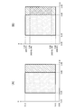
- a suitable relationship between x, y and n is also shown graphically in FIG.
- FIG. 1A is a graph showing the relationship between x and n
- FIG. 1B is a graph showing the relationship between x and y.
- a potassium sodium niobate-based thin film in which M1M2O 3 (BaZrO 3 , BaSnO 3 , BaHfO 3, etc.) is used as the piezoelectric thin film is used. Therefore, an electric field exceeding 100 kV / cm Even when applied to the thin film, a rapid increase in leakage current can be suppressed.
- x, y and n are 0.80 ⁇ x ⁇ 1.00 and 0.85 ⁇ y ⁇ 1.10.
- the piezoelectric thin film element is characterized in that 0.01 ⁇ n ⁇ 0.10.
- x, y and n are 0.80 ⁇ x ⁇ 1.00 and 0.90 ⁇ y ⁇ 1.05, respectively.
- the piezoelectric thin film element is characterized in that 0.01 ⁇ n ⁇ 0.10.
- the hatched portion in FIG. 1A shows the optimum relationship between x and n in the invention according to claim 5 or claim 6.
- the hatched portion in FIG. 1B is a portion showing the optimum relationship between x and y in the invention according to claim 5 or claim 6.
- M1M2O 3 BaZrO 3, BaSnO 3, BaHfO 3 , etc.
- K1M2O 3 BaZrO 3, BaSnO 3, BaHfO 3 , etc.
- a piezoelectric thin film element having excellent leakage current characteristics, ferroelectric characteristics, and piezoelectric characteristics can be obtained.
- (A) is a graph showing the relationship between x and n
- (B) is a graph showing the relationship between x and y.
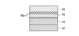
- 1 is a cross-sectional view of a piezoelectric thin film element according to the present invention.
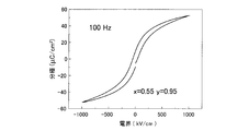
- BaZrO 3 is a graph showing a hysteresis curve of the piezoelectric film element using sodium potassium niobate-based thin film which is a solid solution.
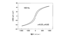
- BaSnO 3 is a graph showing a hysteresis curve of the piezoelectric film element using sodium potassium niobate-based thin film which is a solid solution.
- BaHfO 3 is a graph showing a hysteresis curve of the piezoelectric film element using sodium potassium niobate-based thin film which is a solid solution.
- FIG. 2 is a schematic cross-sectional view of the piezoelectric thin film element according to the first embodiment.
- the piezoelectric thin film element includes a substrate 12, a lower electrode 14 formed on the substrate 12, a piezoelectric thin film 16 formed on the lower electrode 14, and an upper electrode 18 formed on the piezoelectric thin film 16. Has been.
- the BaZrO in the potassium sodium niobate-based thin film represented by the general formula (1-n) (K 1-x Na x ) Nb y O 3 —nBaZrO 3 as the piezoelectric thin film 16 is used.
- the content of 3 has changed.
- a silicon substrate (Si substrate) is used as the substrate 12.
- the substrate 12 may be a glass substrate, a quartz glass substrate, a GaAs substrate, a GaN substrate, a CaF 2 substrate, a sapphire substrate, a MgO substrate, a SrTiO 3 substrate, a LaAlO 3 substrate, a stainless substrate, or the like.
- the piezoelectric thin film 16, that is, the potassium sodium niobate (KNN) thin film 16, is formed by using a chemical solution deposition method.
- n is selected from seven types of 0.00, 0.005, 0.01, 0.03, 0.05, 0.1, and 0.12. .
- raw materials potassium ethoxide, sodium ethoxide, pentaethoxyniobium, manganese acetylacetonate, barium ethoxide, and tetraisopropoxyzirconium are mixed in a 2-methoxyethanol solvent in a glove box.
- the mixed solution is refluxed at 125 ° C. for 16 hours in a nitrogen atmosphere, whereby a 0.3 M potassium sodium niobate (KNN) -based precursor solution (also referred to as a chemical solution deposition solution) is obtained. ).
- KNN potassium sodium niobate
- the organic substance include, but are not limited to, carboxylic anhydrides, dicarboxylic acid monoesters, ⁇ -diketones, glycols, amines, and the like. Further, the organic substance may be added before refluxing or after refluxing.
- the sputtering conditions are a sputtering output of 100 W, a sputtering time of 5 minutes, a temperature of the substrate 12 of 300 ° C., and a degree of vacuum of 5 millitorr.
- a potassium sodium niobate-based precursor solution is spin-coated on the lower electrode 14 in a dry gas.
- the second heat treatment (main heat treatment or firing treatment) is performed. That is, the dried potassium sodium niobate-based precursor film is 5 ° C./min or less in the temperature range of 350 ° C. to 750 ° C. (including the temperature around 500 ° C. at which the complex formed by reflux is rapidly decomposed). The temperature is raised at a rate of temperature rise and baked at a temperature of 750 ° C. for 10 minutes. In this way, the potassium sodium niobate layer 16a is formed. The thickness of the potassium sodium niobate layer 16a formed in one step is 30 nm.
- the above-described step of forming the potassium sodium niobate-based layer 16a is repeated 10 times to obtain (1-n) (K 0.45 Na 0.55 ) Nb 0.95 O 3 —nBaZrO having a thickness of 300 nm.
- a potassium sodium niobate thin film 16 having a composition of 3 is formed.
- the upper electrode 18 is formed on the potassium sodium niobate thin film 16 by a magnetron DC sputtering method.
- a material of the upper electrode 18 Pt or the like is used.
- Table 1 shows the ratio n of BaZrO 3 as 0.00 (sample No. 1), 0.005 (sample No. 2), 0.01 (sample No. 3), 0.03 (sample No. 4). , 0.10 (sample No. 5) and 0.12 (sample No. 6), the electrical characteristics of the piezoelectric thin film element are shown.
- the items of electrical characteristics are insulation, dielectric constant ⁇ , tan ⁇ , and ferroelectric characteristics.
- a leakage current value in an electric field of 200 kV / cm was measured using a measuring device “Electrometer 6517 type” (trade name, manufactured by Keithley).
- the dielectric constant ⁇ and tan ⁇ were measured at 1 kHz when no voltage was applied using a measuring device “HP4284A” (trade name, manufactured by Agilent Technologies).
- Ferroelectric properties are measured using a measuring device “Precision Premier II” (trade name, manufactured by Radiant Technologies, Inc.) using a hysteresis curve with a measurement frequency of 10 kHz and 500 kV / cm.
- the value of spontaneous polarization Ps when measured with the applied voltage was measured.
- sample No. 1, sample no. 3, Sample No. 4 and sample no. 5 was measured using a scanning probe microscope “SPA400” (trade name, manufactured by SII Nanotechnology).
- Z max / V max was obtained from the maximum applied voltage V max obtained by the measurement and the maximum electric field induced strain Z max at that time.
- This value Z max / V max is the piezoelectric constant d 33 * .
- the maximum applied voltage V max is 25 V, and the measurement frequency is 0.5 to 10 Hz.
- the average value of the obtained values is taken as the piezoelectric constant d 33 * of the sample.
- Table 2 The measurement results are shown in Table 2 above.
- sample No. 3 to Sample No. 5 has a piezoelectric constant d 33 * of 117.0 pm / V, 124.7 pm / V, and 120.0 pm / V, respectively. It was a value equivalent to 124.0 pm / V of 1 (without BaZrO 3 ).
- the piezoelectric thin film element of the second embodiment has the same configuration as the piezoelectric thin film element of the first embodiment shown in FIG.
- x in the potassium sodium niobate thin film represented by the general formula (1-n) (K 1-x Na x ) Nb y O 3 —nBaZrO 3 , which is the piezoelectric thin film 16, is used. And y are changing.
- the piezoelectric thin film 16, that is, the potassium sodium niobate (KNN) -based thin film 16 is formed using a chemical solution deposition method.
- the raw materials potassium ethoxide, sodium ethoxide, pentaethoxyniobium, manganese acetylacetonate, barium ethoxide (or calcium ethoxide or strontium ethoxide), and tetraisopropoxyzirconium in molar ratio (1 .07-x) ⁇ 0.97: (x + 0.17) ⁇ 0.97: y ⁇ 0.97: 0.02 ⁇ 0.97: 0.03: 0.03.
- x and y satisfy the conditional expression 0.2 ⁇ x ⁇ 1.00 and the conditional expression 0.8 ⁇ y ⁇ 1.15.
- the substrate 12, the lower electrode 14 formed on the substrate 12, the piezoelectric thin film 16 formed on the lower electrode 14, and the piezoelectric thin film 16 are formed by the same method as in the first embodiment.
- a piezoelectric thin film element composed of the upper electrode 18 thus formed is produced.
- Table 3 Table 4, Table 5 and Table 6 show that x and y in 0.97 (K 1-x Na x ) Nb y O 3 -0.03BaZrO 3 are 0.2 ⁇ x ⁇ 1.00, 0 Leakage current in an electric field of 200 kV / cm when changing in the range of .8 ⁇ y ⁇ 1.15, dielectric constant ⁇ and tan ⁇ at a frequency of 1 kHz, when measured at an applied electric field of 500 kV / cm at a measurement frequency of 10 kHz
- the values of spontaneous polarization Ps are shown (Sample No. 4, Sample No. 7 to Sample No. 141).
- the samples of 0.25 ⁇ x ⁇ 1.00 have a leak current of 1.05 ⁇ 10 ⁇ 7 A / cm 2 to 2.69 ⁇ 10 ⁇ 7 A / cm 2 . These values are obtained from Sample No. which does not contain BaZrO 3 . Compared to 1, a significant improvement in leakage current was observed. Further, the spontaneous polarization Ps was 20 to 27 ⁇ C / cm 2 and the ferroelectric characteristics were maintained. Therefore, the samples of 0.25 ⁇ x ⁇ 1.00 (Sample No. 42 to Sample No. 57) were determined to be non-defective products (G).
- the samples of 0.25 ⁇ x ⁇ 1.00 have a leakage current of 1.19 ⁇ 10 ⁇ 6 A / cm 2 to 9.68 ⁇ . 10 ⁇ 6 A / cm 2 .
- These values are obtained from Sample No. which does not contain BaZrO 3 .
- a significant improvement in leakage current was observed.
- the spontaneous polarization Ps was 18 to 22 ⁇ C / cm 2 and the ferroelectric characteristics were maintained. Therefore, the samples of 0.25 ⁇ x ⁇ 1.00 (Sample No. 4 and Sample No. 59 to Sample No. 73) were determined to be non-defective products (G).
- the samples of 0.25 ⁇ x ⁇ 1.00 have a leakage current of 1.19 ⁇ 10 ⁇ 6 A / cm 2 to 8.51 ⁇ 10 ⁇ 6 A / cm 2 .
- These values are obtained from Sample No. which does not contain BaZrO 3 .
- Compared to 1 a significant improvement in leakage current was observed.
- the spontaneous polarization Ps was 16 to 24 ⁇ C / cm 2 and maintained the ferroelectric characteristics. Therefore, the samples of 0.25 ⁇ x ⁇ 1.00 (Sample No. 75 to Sample No. 90) were determined to be non-defective products (G).
- the electric field induced strain Z of the sample (sample No. 4, sample No. 25 to sample No. 40, etc.) determined to be non-defective (G) by the above-mentioned non-defective / defective (G / NG) determination is scanned. It was measured using a scanning probe microscope “SPA400” (trade name, manufactured by SII Nanotechnology).
- Z max / V max was obtained from the maximum applied voltage V max obtained by the measurement and the maximum electric field induced strain Z max at that time.
- This value Z max / V max is the piezoelectric constant d 33 * .
- the maximum applied voltage V max is 25 V, and the measurement frequency is 0.5 to 10 Hz.
- the average value of the obtained values is taken as the piezoelectric constant d 33 * of the sample.
- the piezoelectric constant d 33 * is 100.5 to 160.8 pm / V. It can be seen that a numerical value equal to or higher than 124.0 pm / V of 1 (without BaZrO 3 ) is obtained.
- a sample in which the range of x is 0.80 ⁇ x ⁇ 1.00 has a piezoelectric constant d 33 * of 140.5 to 160.8 pm / V. No. Compared with 124.0 pm / V of 1 (without BaZrO 3 ), it can be seen that this is a very large numerical value.
- M1 Ca, Sr
- the value of 33 * is shown (Sample Nos. 142 and 143).
- M1 Ca, Sr, Ba
- the thickness is 10.10, a piezoelectric thin film element having excellent leakage current characteristics, ferroelectric characteristics, and piezoelectric characteristics can be obtained. Furthermore, the temperature change of the capacitance that becomes a problem when using the ferroelectric thin film element and the piezoelectric thin film element can be suppressed.
- the piezoelectric thin film element of the third embodiment has the same configuration as the piezoelectric thin film element of the first embodiment shown in FIG.
- the BaSnO in the potassium sodium niobate-based thin film represented by the general formula (1-n) (K 1-x Na x ) Nb y O 3 -nBaSnO 3 as the piezoelectric thin film 16 is used.
- the content of 3 has changed.
- the raw materials potassium ethoxide, sodium ethoxide, pentaethoxyniobium, manganese acetylacetonate, barium ethoxide, and tetraisopropoxytin are in a molar ratio of 0.52 ⁇ (1-n): 0.72.
- X (1-n): 0.95 x (1-n): 0.02 x (1-n): n: n is prepared.
- n is selected from seven types of 0.00, 0.005, 0.01, 0.03, 0.05, 0.1, and 0.12. .
- raw materials potassium ethoxide, sodium ethoxide, pentaethoxyniobium, manganese acetylacetonate, barium ethoxide, and tetraisopropoxytin are mixed in a 2-methoxyethanol solvent in a glove box.
- the mixed solution is refluxed at 125 ° C. for 16 hours in a nitrogen atmosphere, whereby a 0.3 M potassium sodium niobate (KNN) -based precursor solution (also referred to as a chemical solution deposition solution) is obtained. ).
- KNN potassium sodium niobate
- the organic substance include, but are not limited to, carboxylic anhydrides, dicarboxylic acid monoesters, ⁇ -diketones, glycols, amines, and the like. Further, the organic substance may be added before refluxing or after refluxing.
- the lower electrode 14 is formed on the Si substrate 12 by magnetron DC sputtering.
- a material of the lower electrode 14 Pt or the like is used.
- a potassium sodium niobate-based precursor solution is spin-coated on the lower electrode 14 in a dry gas.
- the first heat treatment (preliminary heat treatment or drying treatment) is performed. That is, the potassium sodium niobate precursor solution applied on the lower electrode 14 is rapidly heated using a hot plate heated to 350 ° C. in advance and dried at 350 ° C. for 3 minutes.
- the above-described step of forming the potassium sodium niobate-based layer 16a is repeated 10 times to obtain (1-n) (K 0.45 Na 0.55 ) Nb 0.95 O 3 —nBaSnO having a thickness of 300 nm.
- a potassium sodium niobate thin film 16 having a composition of 3 is formed.
- the upper electrode 18 is formed on the potassium sodium niobate thin film 16 by a magnetron DC sputtering method.
- a material of the upper electrode 18 Pt or the like is used.
- the sputtering conditions are a sputtering output of 100 W, a sputtering time of 5 minutes, a temperature of the substrate 12 of 150 ° C., and a degree of vacuum of 5 millitorr. In this way, a piezoelectric thin film element is obtained.
- composition of the potassium sodium niobate-based thin film 16 was confirmed to be the target by inductively coupled plasma composition analysis.
- Table 11 shows the ratio n of BaSnO 3 in 0.00 (sample No. 201), 0.005 (sample No. 202), 0.01 (sample No. 203), and 0.03 (sample No. 204). , 0.10 (sample No. 205) and 0.12 (sample No. 206), the electrical characteristics of the piezoelectric thin film element are shown.
- the items of electrical characteristics are insulation, dielectric constant ⁇ , tan ⁇ , and ferroelectric characteristics.
- sample no. 201-Sample No. A piezoelectric constant d 33 * of 206 was obtained in the same manner as in the first embodiment. The measurement results are shown in Table 12.
- the piezoelectric constants d 33 * of 205 are 119.2 pm / V, 115.3 pm / V, 107.9 pm / V, and 112.6 pm / V, respectively. The value was equal to 124.0 pm / V of 201 (without BaSnO 3 ).
- a sample containing 2 mol of Mn with respect to 100 mol of (K 0.45 Na 0.55 ) Nb 0.95 O 3 was evaluated.
- a sample containing 10 mol or less of Mn with respect to 100 mol of the main component (1-n) (K 0.45 Na 0.55 ) Nb 0.95 O 3 —nBaSnO 3 was also applied to the third sample. Evaluation results similar to those of the embodiment were obtained.
- x in the potassium sodium niobate-based thin film represented by the general formula (1-n) (K 1-x Na x ) Nb y O 3 —nBaSnO 3 , which is the piezoelectric thin film 16, is used. And y are changing.
- the piezoelectric thin film 16, that is, the potassium sodium niobate (KNN) -based thin film 16 is formed using a chemical solution deposition method.
- the raw materials potassium ethoxide, sodium ethoxide, pentaethoxyniobium, manganese acetylacetonate, barium ethoxide, and tetraisopropoxytin are (1.07-x) ⁇ 0.97 :( x + 0.17) ⁇ 0.97: y ⁇ 0.97: 0.02 ⁇ 0.97: 0.03: 0.03.
- x and y satisfy the conditional expression 0.2 ⁇ x ⁇ 1.00 and the conditional expression 0.85 ⁇ y ⁇ 1.10.
- the substrate 12, the lower electrode 14 formed on the substrate 12, the piezoelectric thin film 16 formed on the lower electrode 14, and the piezoelectric thin film 16 are formed.
- a piezoelectric thin film element composed of the upper electrode 18 thus formed is produced.
- the piezoelectric thin film 16 has a thickness of 300 nm and a composition of 0.97 (K 1-x Na x ) Nb y O 3 ⁇ 0.03BaSnO 3 (0.2 ⁇ x ⁇ 1.00, 0.85 ⁇ y ⁇ 1.10) potassium sodium niobate (KNN) -based thin film.
- Tables 13, 14 and 15 show that x and y in 0.97 (K 1-x Na x ) Nb y O 3 -0.03BaSnO 3 are 0.2 ⁇ x ⁇ 1.00 and 0.85 ⁇ Leakage current in an electric field of 200 kV / cm when changing in the range of y ⁇ 1.10, permittivity ⁇ and tan ⁇ at a frequency of 1 kHz, spontaneous polarization Ps when measured at an applied electric field of 500 kV / cm at a measurement frequency of 10 kHz (Sample No. 204, Sample No. 207 to Sample No. 307).
- the non-defective product (G) when the leakage current is 5.43 ⁇ 10 ⁇ 5 A / cm 2 or less and the spontaneous polarization Ps is 10 ⁇ C / cm 2 or more, the non-defective product (G) In other cases, it was determined as a defective product (NG).
- the samples of 0.25 ⁇ x ⁇ 1.00 (Sample No. 225 to Sample No. 240) have a leakage current of 7.88 ⁇ 10 ⁇ 7 A / cm 2 to 2.77 ⁇ 10 ⁇ 6 A / cm 2 . These values are obtained from Sample No. which does not contain BaSnO 3 . Compared to 201, a significant improvement in leakage current was observed. Furthermore, the spontaneous polarization Ps was 15 to 32 ⁇ C / cm 2 and the ferroelectric characteristics were maintained. Therefore, the samples of 0.25 ⁇ x ⁇ 1.00 (Sample No. 225 to Sample No. 240) were determined to be non-defective products (G).
- the samples of 0.25 ⁇ x ⁇ 1.00 have a leakage current of 1.17 ⁇ 10 ⁇ 7 A / cm 2 to 8.47 ⁇ . 10 ⁇ 6 A / cm 2 .
- These values are obtained from Sample No. which does not contain BaSnO 3 .
- a significant improvement in leakage current was observed.
- the spontaneous polarization Ps was 14 to 25 ⁇ C / cm 2 and the ferroelectric characteristics were maintained. Therefore, the samples of 0.25 ⁇ x ⁇ 1.00 (Sample No. 204 and Sample No. 242 to Sample No. 256) were determined to be non-defective products (G).
- NG defective product
- the samples of 0.25 ⁇ x ⁇ 1.00 have a leakage current of 1.07 ⁇ 10 ⁇ 6 A / cm 2 to 1.30 ⁇ 10 ⁇ 5 A / cm 2 .
- These values are obtained from Sample No. which does not contain BaSnO 3 .
- a significant improvement in leakage current was observed.
- the spontaneous polarization Ps was 15 to 26 ⁇ C / cm 2 and the ferroelectric characteristics were maintained. Therefore, the samples of 0.25 ⁇ x ⁇ 1.00 (Sample No. 258 to Sample No. 273) were determined to be non-defective products (G).
- the samples of 0.25 ⁇ x ⁇ 1.00 (Sample No. 275 to Sample No. 290) have a leakage current of 1.12 ⁇ 10 ⁇ 6 A / cm 2 to 4.60 ⁇ 10 ⁇ 5 A / cm 2 . These values are obtained from Sample No. which does not contain BaSnO 3 . Compared to 201, a significant improvement in leakage current was observed. Further, the spontaneous polarization Ps was 17 to 24 ⁇ C / cm 2 and maintained the ferroelectric characteristics. Therefore, the samples of 0.25 ⁇ x ⁇ 1.00 (Sample No. 275 to Sample No. 290) were determined to be non-defective products (G).
- the piezoelectric constant d 33 * of a sample (sample No. 204, sample No. 225 to sample No. 240, etc.) determined to be non-defective (G) by the above-mentioned non-defective / defective (G / NG) determination is It was obtained in the same manner as in the second embodiment.
- the measurement results are shown in Table 16 and Table 17.
- M1 Ca, Sr
- the value of 33 * is shown (Sample Nos. 308 and 309).
- FIG. 204 shows a ferroelectric hysteresis curve of 204
- Potassium sodium niobate-based thin film with x, y and n ranges of 0.25 ⁇ x ⁇ 1.00, 0.90 ⁇ y ⁇ 1.05 and 0.01 ⁇ n ⁇ 0, respectively
- the thickness to 10.10, a piezoelectric thin film element having excellent leakage current characteristics, ferroelectric characteristics, and piezoelectric characteristics can be obtained.
- the temperature change of the capacitance that becomes a problem when using the ferroelectric thin film element and the piezoelectric thin film element can be suppressed.
- the piezoelectric thin film element of the fifth embodiment has the same configuration as the piezoelectric thin film element of the first embodiment shown in FIG.
- the BaHfO in the potassium sodium niobate-based thin film represented by the general formula (1-n) (K 1-x Na x ) Nb y O 3 -nBaHfO 3 as the piezoelectric thin film 16 is used.
- the content of 3 has changed.
- the piezoelectric thin film 16, that is, the potassium sodium niobate (KNN) thin film 16, is formed by using a chemical solution deposition method.
- raw materials potassium ethoxide, sodium ethoxide, pentaethoxyniobium, manganese acetylacetonate, barium ethoxide, and tetraisopropoxyhafnium are mixed in a 2-methoxyethanol solvent in a glove box.
- the mixed solution is refluxed at 125 ° C. for 16 hours in a nitrogen atmosphere, whereby a 0.3 M potassium sodium niobate (KNN) -based precursor solution (also referred to as a chemical solution deposition solution) is obtained. ).
- KNN potassium sodium niobate
- the organic substance include, but are not limited to, carboxylic anhydrides, dicarboxylic acid monoesters, ⁇ -diketones, glycols, amines, and the like. Further, the organic substance may be added before refluxing or after refluxing.
- the lower electrode 14 is formed on the Si substrate 12 by magnetron DC sputtering.
- a material of the lower electrode 14 Pt or the like is used.
- the sputtering conditions are a sputtering output of 100 W, a sputtering time of 5 minutes, a temperature of the substrate 12 of 300 ° C., and a degree of vacuum of 5 millitorr.
- a potassium sodium niobate-based precursor solution is spin-coated on the lower electrode 14 in a dry gas.
- the second heat treatment (main heat treatment or firing treatment) is performed. That is, the dried potassium sodium niobate-based precursor film is 5 ° C./min or less in the temperature range of 350 ° C. to 750 ° C. (including the temperature around 500 ° C. at which the complex formed by reflux is rapidly decomposed). The temperature is raised at a rate of temperature rise and baked at a temperature of 750 ° C. for 10 minutes. In this way, the potassium sodium niobate layer 16a is formed. The thickness of the potassium sodium niobate layer 16a formed in one step is 30 nm.
- the above-described step of forming the potassium sodium niobate-based layer 16a is repeated 10 times to obtain (1-n) (K 0.45 Na 0.55 ) Nb 0.95 O 3 —nBaHfO having a thickness of 300 nm.
- a potassium sodium niobate thin film 16 having a composition of 3 is formed.
- the upper electrode 18 is formed on the potassium sodium niobate thin film 16 by a magnetron DC sputtering method.
- a material of the upper electrode 18 Pt or the like is used.
- the sputtering conditions are a sputtering output of 100 W, a sputtering time of 5 minutes, a temperature of the substrate 12 of 150 ° C., and a degree of vacuum of 5 millitorr. In this way, a piezoelectric thin film element is obtained.
- composition of the potassium sodium niobate-based thin film 16 was confirmed to be the target by inductively coupled plasma composition analysis.
- Table 19 shows the ratio n of BaHfO 3 as 0.00 (sample No. 401), 0.005 (sample No. 402), 0.01 (sample No. 403), 0.03 (sample No. 404). , 0.10 (sample No. 405) and 0.12 (sample No. 406), the electrical characteristics of the piezoelectric thin film element are shown.
- the items of electrical characteristics are insulation, dielectric constant ⁇ , tan ⁇ , and ferroelectric characteristics.
- Sample No. Since 406 (n 0.12) has a spontaneous polarization Ps of less than 10 ⁇ C / cm 2 , it was determined as a defective product (NG).
- sample no. No. 402 has a leakage current of 2.38 ⁇ 10 ⁇ 4 A / cm 2 . It was almost the same as the leakage current of 401 (without BaHfO 3 ) of 5.43 ⁇ 10 ⁇ 4 A / cm 2 .
- sample no. 403, Sample No. 404, Sample No. 405, Sample No. 406 has leakage currents of 8.22 ⁇ 10 ⁇ 6 A / cm 2 , 6.15 ⁇ 10 ⁇ 6 A / cm 2 , 3.61 ⁇ 10 ⁇ 6 A / cm 2 , and 1.73 ⁇ 10 ⁇ , respectively. 6 A / cm 2 , and good leakage current characteristics were obtained.
- the piezoelectric constant d 33 * of 405 is 120.6 pm / V, 123.7 pm / V, 128.7 pm / V, and 111.9 pm / V, respectively. It was a value equivalent to 124.0 pm / V of 401 (without BaHfO 3 ).
- the piezoelectric thin film element of the sixth embodiment has the same configuration as the piezoelectric thin film element of the first embodiment shown in FIG.
- x in the potassium sodium niobate-based thin film represented by the general formula (1-n) (K 1-x Na x ) Nb y O 3 —nBaHfO 3 that is the piezoelectric thin film 16 is used. And y are changing.
- the piezoelectric thin film 16, that is, the potassium sodium niobate (KNN) -based thin film 16 is formed using a chemical solution deposition method.
- raw materials potassium ethoxide, sodium ethoxide, pentaethoxyniobium, manganese acetylacetonate, barium ethoxide, and tetraisopropoxyhafnium are (1.07 ⁇ x) ⁇ 0.97 :( x + 0.17) ⁇ 0.97: y ⁇ 0.97: 0.02 ⁇ 0.97: 0.03: 0.03.
- x and y satisfy the conditional expression 0.2 ⁇ x ⁇ 1.00 and the conditional expression 0.85 ⁇ y ⁇ 1.10.
- the substrate 12, the lower electrode 14 formed on the substrate 12, the piezoelectric thin film 16 formed on the lower electrode 14, and the piezoelectric thin film 16 are formed by the same method as in the fifth embodiment.
- a piezoelectric thin film element composed of the upper electrode 18 thus formed is produced.
- the piezoelectric thin film 16 has a thickness of 300 nm and a composition of 0.97 (K 1-x Na x ) Nb y O 3 ⁇ 0.03BaHfO 3 (0.2 ⁇ x ⁇ 1.00, 0.85 ⁇ y ⁇ 1.10) potassium sodium niobate (KNN) -based thin film.
- Table 21, Table 22, and Table 23 show that x and y in 0.97 (K 1-x Na x ) Nb y O 3 -0.03BaHfO 3 are 0.2 ⁇ x ⁇ 1.00 and 0.85 ⁇ Leakage current in an electric field of 200 kV / cm when changing in the range of y ⁇ 1.10, permittivity ⁇ and tan ⁇ at a frequency of 1 kHz, spontaneous polarization Ps when measured at an applied electric field of 500 kV / cm at a measurement frequency of 10 kHz (Sample No. 404, Sample No. 407 to Sample No. 507).
- the non-defective product (G) when the leakage current is 5.43 ⁇ 10 ⁇ 5 A / cm 2 or less and the spontaneous polarization Ps is 10 ⁇ C / cm 2 or more, the non-defective product (G) In other cases, it was determined as a defective product (NG).
- the samples of 0.25 ⁇ x ⁇ 1.00 have a leakage current of 2.22 ⁇ 10 ⁇ 8 A / cm 2 to 6.81 ⁇ 10 ⁇ 6 A / cm 2 . These values are obtained from Sample No. which does not contain BaHfO 3 . Compared with 401, a significant improvement in leakage current was observed. Further, the spontaneous polarization Ps was 18 to 26 ⁇ C / cm 2 and the ferroelectric characteristics were maintained. Therefore, the samples of 0.25 ⁇ x ⁇ 1.00 (Sample No. 425 to Sample No. 440) were determined as non-defective products (G).
- the samples of 0.25 ⁇ x ⁇ 1.00 have a leak current of 1.69 ⁇ 10 ⁇ 7 A / cm 2 to 7.42 ⁇ . 10 ⁇ 6 A / cm 2 .
- These values are obtained from Sample No. which does not contain BaHfO 3 .
- a significant improvement in leakage current was observed.
- the spontaneous polarization Ps was 19 to 24 ⁇ C / cm 2 and the ferroelectric characteristics were maintained. Therefore, the samples of 0.25 ⁇ x ⁇ 1.00 (Sample No. 404 and Sample No. 442 to Sample No. 456) were determined to be non-defective products (G).
- NG defective product
- the samples of 0.25 ⁇ x ⁇ 1.00 have a leakage current of 2.64 ⁇ 10 ⁇ 6 A / cm 2 to 9.71 ⁇ 10 ⁇ 6 A / cm 2 .
- These values are obtained from Sample No. which does not contain BaHfO 3 .
- the spontaneous polarization Ps was 20 to 25 ⁇ C / cm 2 and the ferroelectric characteristics were maintained. Therefore, the samples of 0.25 ⁇ x ⁇ 1.00 (Sample No. 458 to Sample No. 473) were determined to be non-defective products (G).
- the samples of 0.25 ⁇ x ⁇ 1.00 (Sample No. 475 to Sample No. 490) have a leakage current of 1.26 ⁇ 10 ⁇ 6 A / cm 2 to 8.22 ⁇ 10 ⁇ 6 A / cm 2 . These values are obtained from Sample No. which does not contain BaHfO 3 . Compared with 401, a significant improvement in leakage current was observed. Furthermore, the spontaneous polarization Ps was 20 to 24 ⁇ C / cm 2 and maintained the ferroelectric characteristics. Therefore, the samples of 0.25 ⁇ x ⁇ 1.00 (sample No. 475 to sample No. 490) were determined to be non-defective products (G).
- the piezoelectric constant d 33 * of a sample (sample No. 404, sample No. 425 to sample No. 440, etc.) determined to be non-defective (G) by the above-mentioned non-defective / defective (G / NG) determination is It was obtained in the same manner as in the second embodiment.
- the measurement results are shown in Table 24 and Table 25.
- the piezoelectric constant d 33 * is 102.3 to 158.6 pm / V. It can be seen that 401 (without BaHfrO 3 ) is almost the same as 124.0 pm / V. This is because the value of the spontaneous polarization Ps is a large value of 10 ⁇ C / cm 2 or more.
- a sample in which the range of x is 0.80 ⁇ x ⁇ 1.00 has a piezoelectric constant d 33 * of 140.3 to 158.6 pm / V. No. Compared to 124.0 pm / V of 401 (without BaHfO 3 ), it can be seen that this is a very large numerical value.
- M1 Ca, Sr
- the value of 33 * is shown (Sample Nos. 508 and 509).
- the leakage current characteristic, the ferroelectric characteristic and the piezoelectric characteristic can be obtained. It was revealed that an excellent piezoelectric thin film element can be obtained.
- FIG. A ferroelectric hysteresis curve 404 is shown.
- the leakage current characteristics in an electric field of 100 kV / cm or more are improved, and a good ferroelectric hysteresis curve is exhibited even at a maximum applied voltage of 1 MV / cm and a measurement frequency of 100 Hz. I understand.
- this invention is not limited to the said embodiment, In the range of the summary, it deform
- the potassium sodium niobate thin film 16 is formed by chemical solution deposition, if the composition of the prepared potassium sodium niobate thin film 16 is within the scope of the present invention, for example, sputtering, chemical vapor deposition Alternatively, it may be formed by an aerosol deposition method, a pulse laser deposition method, or the like.
Landscapes
- Chemical & Material Sciences (AREA)
- Engineering & Computer Science (AREA)
- Materials Engineering (AREA)
- Ceramic Engineering (AREA)
- Organic Chemistry (AREA)
- Manufacturing & Machinery (AREA)
- Physics & Mathematics (AREA)
- Inorganic Chemistry (AREA)
- Thermal Sciences (AREA)
- General Chemical & Material Sciences (AREA)
- Chemical Kinetics & Catalysis (AREA)
- Mechanical Engineering (AREA)
- Metallurgy (AREA)
- Structural Engineering (AREA)
- Dispersion Chemistry (AREA)
- Compositions Of Oxide Ceramics (AREA)
- Inorganic Compounds Of Heavy Metals (AREA)
- Inorganic Insulating Materials (AREA)
Abstract
【課題】優れた電気特性を有する圧電体薄膜素子を提供する。 【解決手段】圧電体薄膜素子は、基板12、基板上に形成された下部電極14、下部電極上に形成された圧電体薄膜16、および、圧電体薄膜上に形成された上部電極18にて構成されている。圧電体薄膜は、一般式(1-n)(K1-xNax)NbyO3-nM1M2O3で表されると共に、M1がCa、SrおよびBaのいずれか一つであり、M2がZrであるものを主成分とするニオブ酸カリウムナトリウム系薄膜であって、x、yおよびnが、それぞれ、0.25≦x≦1.00、0.85≦y≦1.10、0.01≦n≦0.10の範囲である。あるいは、圧電体薄膜16は、一般式(1-n)(K1-xNax)NbyO3-nM1M2O3で表されると共に、M1がCa、SrおよびBaのいずれか一つであり、M2がSnおよびHfのいずれか一つであるものを主成分とするニオブ酸カリウムナトリウム系薄膜であって、x、yおよびnが、それぞれ、0.25≦x≦1.00、0.90≦y≦1.05、0.01≦n≦0.10の範囲である。
Description
本発明は、アクチュエータやセンサなどに用いられる圧電体薄膜素子に関する。
圧電体は、現在、アクチュエータやセンサなどの機能性電子部品の材料として幅広く利用されている。これらの用途に用いられる圧電体材料として、PZTと称される一般式Pb(Zr,Ti)O3で表示されるペロブスカイト型強誘電体材料が、主に用いられている。ところが、PZTは、有害なPb(鉛)を含んでいるため、自然環境の保護上好ましくない材料である。
そこで、現在、様々な非鉛圧電体材料の研究開発が活発に行われている。この非鉛圧電体材料の中の一つが、KNNと称される一般式(K,Na)NbO3で表示されるペロブスカイト型強誘電体材料である。KNN(ニオブ酸カリウムナトリウム)は、PZTに匹敵する圧電特性を示すため、非常に注目されている。
例えば、特許文献1には、スパッタリング法によって作成された、(K1-xNax)NbO3(0<x<1)で表示されるニオブ酸カリウムナトリウム薄膜が提案されている。そして、特許文献1には、平均結晶粒径が0.1μm~1.0μmで、かつ、結晶粒が基板の厚さ方向に長いニオブ酸カリウムナトリウム(KNN)薄膜を作成することにより、大きな圧電定数を得ることができることが開示されている。
また、非特許文献1には、化学溶液堆積(Chemical solution deposition;CSD)法によって作成された、化学量論的なK0.5Na0.5NbO3薄膜およびKとNaをそれぞれ10mol%過剰に添加した組成の薄膜が提案されている。そして、非特許文献1には、KとNaをそれぞれ10mol%過剰に添加することで、リーク電流特性の改善が認められることが開示されている。
応用物理日本ジャーナル(Japanese Journal of Applied Physics)、第49巻、2010年、095805
しかし、従来のニオブ酸カリウムナトリウム薄膜は、100kV/cmの電界印加で、リーク電流が10-7~10-6A/cm2と、十分低いけれども、電界が100kV/cmを越えると、リーク電流が急激に上昇し、200kV/cmの電界印加で、10-2A/cm2以上になるという問題がある。そのため、リーク電流特性および圧電体特性の両方に優れたニオブ酸カリウムナトリウム薄膜はなかった。例えば、特許文献1の(K1-xNax)NbO3(0<x<1)の組成の薄膜は、ニオブ酸カリウムナトリウムが難焼結性であるため、リーク電流特性が悪い。具体的には、200kV/cmの電界印加で、リーク電流は10-1A/cm2である。さらに、強誘電体ヒステリシス曲線が測定されているけれども、良好な強誘電体特性は得られていない。
さらに、非特許文献1のKとNaをそれぞれ10mol%過剰に添加した組成のニオブ酸カリウムナトリウム薄膜は、200kV/cmの電界印加で、リーク電流は約10-2A/cm2である。
それゆえに、本発明の目的は、優れた電気特性、特に、リーク電流特性、強誘電体特性および圧電体特性に優れた圧電体薄膜素子を提供することである。
請求項1に係る発明は、電極と圧電体薄膜とを備えた圧電体薄膜素子であって、圧電体薄膜が、一般式(1-n)(K1-xNax)NbyO3-nBaZrO3で表示されるニオブ酸カリウムナトリウム系薄膜であって、x、yおよびnが、それぞれ、0.25≦x≦0.75、0.85≦y≦1.10、0.01≦n≦0.10の範囲であること、を特徴とする、圧電体薄膜素子である。
また、請求項2に係る発明は、電極と圧電体薄膜とを備えた圧電体薄膜素子であって、圧電体薄膜が、一般式(1-n)(K1-xNax)NbyO3-nBaSnO3で表示されるニオブ酸カリウムナトリウム系薄膜であって、x、yおよびnが、それぞれ、0.25≦x≦0.75、0.90≦y≦1.05、0.01≦n≦0.10の範囲であること、を特徴とする、圧電体薄膜素子である。
また、請求項3に係る発明は、電極と圧電体薄膜とを備えた圧電体薄膜素子であって、圧電体薄膜が、一般式(1-n)(K1-xNax)NbyO3-nM1M2O3で表されると共に、M1がCa、SrおよびBaのいずれか一つであり、M2がZrであるものを主成分とするニオブ酸カリウムナトリウム系薄膜であって、x、yおよびnが、それぞれ、0.25≦x≦1.00、0.85≦y≦1.10、0.01≦n≦0.10の範囲であること、を特徴とする、圧電体薄膜素子である。
また、請求項4に係る発明は、電極と圧電体薄膜とを備えた圧電体薄膜素子であって、圧電体薄膜が、一般式(1-n)(K1-xNax)NbyO3-nM1M2O3で表されると共に、M1がCa、SrおよびBaのいずれか一つであり、M2がSnおよびHfのいずれか一つであるものを主成分とするニオブ酸カリウムナトリウム系薄膜であって、x、yおよびnが、それぞれ、0.25≦x≦1.00、0.90≦y≦1.05、0.01≦n≦0.10の範囲であること、を特徴とする、圧電体薄膜素子である。
ここで、ニオブ酸カリウムナトリウムとM1M2O3(BaZrO3、BaSnO3、BaHfO3など)とは、共にぺロブスカイト構造である。すなわち、KとNaとM1(Ca、Sr、Ba)とが同じサイト(Aサイト)に存在し、NbとM2(Zr、Sn、Hf)とが同じサイト(Bサイト)に存在する。ニオブ酸カリウムナトリウムとM1M2O3(BaZrO3、BaSnO3、BaHfO3など)とは、圧電体薄膜内に均一に分散しているが、これに限るものではない。
また、x、yおよびnの適した関係が、図1にグラフ化して示されている。図1(A)はxとnの関係を示すグラフであり、(B)はxとyの関係を示すグラフである。
また、x、yおよびnの適した関係が、図1にグラフ化して示されている。図1(A)はxとnの関係を示すグラフであり、(B)はxとyの関係を示すグラフである。
本発明では、圧電体薄膜として、M1M2O3(BaZrO3、BaSnO3、BaHfO3など)が固溶されたニオブ酸カリウムナトリウム系薄膜が用いられているため、100kV/cmを超える電界が、圧電体薄膜に印加されても、急激なリーク電流の上昇が抑えられる。
また、請求項5に係る発明は、請求項3に記載の圧電体薄膜素子において、x、yおよびnが、それぞれ、0.80≦x≦1.00、0.85≦y≦1.10、0.01≦n≦0.10の範囲であること、を特徴とする、圧電体薄膜素子である。
また、請求項6に係る発明は、請求項4に記載の圧電体薄膜素子において、x、yおよびnが、それぞれ、0.80≦x≦1.00、0.90≦y≦1.05、0.01≦n≦0.10の範囲であること、を特徴とする、圧電体薄膜素子である。
図1(A)の斜線部分は、請求項5もしくは請求項6に係る発明の、xとnの最適な関係を示す部分である。図1(B)の斜線部分は、請求項5もしくは請求項6に係る発明の、xとyの最適な関係を示す部分である。
本発明では、M1M2O3(BaZrO3、BaSnO3、BaHfO3など)が固溶されないニオブ酸カリウムナトリウム系薄膜の圧電定数d33 *の数値以上の圧電定数d33 *が得られる。
本発明では、M1M2O3(BaZrO3、BaSnO3、BaHfO3など)が固溶されないニオブ酸カリウムナトリウム系薄膜の圧電定数d33 *の数値以上の圧電定数d33 *が得られる。
本発明によれば、リーク電流特性、強誘電体特性および圧電体特性に優れた圧電体薄膜素子が得られる。
この発明の上述の目的,その他の目的,特徴および利点は、図面を参照して行う以下の発明を実施するための形態の説明から一層明らかとなろう。
12 基板
14 下部電極
16 ニオブ酸カリウムナトリウム薄膜
16a ニオブ酸カリウムナトリウム層
18 上部電極
14 下部電極
16 ニオブ酸カリウムナトリウム薄膜
16a ニオブ酸カリウムナトリウム層
18 上部電極
(第1の実施の形態の圧電体薄膜素子の製造)
図2は、第1の実施の形態の圧電体薄膜素子の概略構成断面図である。圧電体薄膜素子は、基板12、基板12上に形成された下部電極14、下部電極14上に形成された圧電体薄膜16、および、圧電体薄膜16上に形成された上部電極18にて構成されている。
図2は、第1の実施の形態の圧電体薄膜素子の概略構成断面図である。圧電体薄膜素子は、基板12、基板12上に形成された下部電極14、下部電極14上に形成された圧電体薄膜16、および、圧電体薄膜16上に形成された上部電極18にて構成されている。
なお、第1の実施の形態では、圧電体薄膜16である一般式(1-n)(K1-xNax)NbyO3-nBaZrO3で表示されるニオブ酸カリウムナトリウム系薄膜におけるBaZrO3の含有量が変化している。
基板12は、例えば、シリコン基板(Si基板)が用いられる。なお、基板12は、ガラス基板、石英ガラス基板、GaAs基板、GaN基板、CaF2基板、サファイア基板、MgO基板、SrTiO3基板、LaAlO3基板、ステンレス基板などの基板を用いてもよい。
圧電体薄膜16、すなわち、ニオブ酸カリウムナトリウム(KNN)系薄膜16は、化学溶液堆積法を用いて作成される。
まず、原料であるカリウムエトキシド、ナトリウムエトキシド、ペンタエトキシニオブ、マンガンアセチルアセトナト、バリウムエトキシド、および、テトライソプロポキシジルコニウムが、モル比で0.52×(1-n):0.72×(1-n):0.95×(1-n):0.02×(1-n):n:nとなるように準備される。ここで、本第1の実施の形態の場合、nは、0.00、0.005、0.01、0.03、0.05、0.1、0.12の7種類が選択される。
次に、原料のカリウムエトキシド、ナトリウムエトキシド、ペンタエトキシニオブ、マンガンアセチルアセトナト、バリウムエトキシド、および、テトライソプロポキシジルコニウムが、グローブボックスの中で、2-メトキシエタノール溶媒に混合される。
次に、その混合溶液は、窒素雰囲気中において、125℃で16時間還流されることによって、濃度が0.3Mのニオブ酸カリウムナトリウム(KNN)系前駆体溶液(化学溶液堆積用溶液とも称される)とされる。
なお、この前駆体溶液に、アルコキシドの安定化剤として一般的に用いられている有機物を添加しても良い。
有機物の種類としては、例えば、無水カルボン酸類、ジカルボン酸モノエステル類、β-ジケトン類、グリコール類、アミン類などが挙げられるが、これに限定されるものではない。また、有機物は還流前に添加しても良いし、還流後に添加しても良い。
なお、この前駆体溶液に、アルコキシドの安定化剤として一般的に用いられている有機物を添加しても良い。
有機物の種類としては、例えば、無水カルボン酸類、ジカルボン酸モノエステル類、β-ジケトン類、グリコール類、アミン類などが挙げられるが、これに限定されるものではない。また、有機物は還流前に添加しても良いし、還流後に添加しても良い。
一方、下部電極14が、Si基板12上に、マグネトロンDCスパッタリング法によって形成される。下部電極14の材料としては、Ptなどが用いられる。
スパッタリング条件は、スパッタ出力が100W、スパッタ時間が5分、基板12の温度が300℃、真空度が5ミリtorrである。
次に、ニオブ酸カリウムナトリウム系前駆体溶液が、乾燥ガス中において、下部電極14上にスピンコート塗布される。
次に、第一熱処理(予備熱処理または乾燥処理)が実行される。すなわち、下部電極14上に塗布されたニオブ酸カリウムナトリウム系前駆体溶液が、予め350℃の温度に加熱されたホットプレートを用いて、急速に昇温され、350℃で3分間乾燥される。
次に、第二熱処理(本熱処理または焼成処理)が実行される。すなわち、乾燥されたニオブ酸カリウムナトリウム系前駆体膜は、350℃~750℃の温度範囲(還流により形成される錯体が急激に分解する温度500℃付近を含む)において、5℃/分以下の昇温速度で昇温され、750℃の温度で10分間焼成される。こうして、ニオブ酸カリウムナトリウム系層16aが形成される。前記工程1回で形成されるニオブ酸カリウムナトリウム系層16aの厚みは、30nmである。
さらに、ニオブ酸カリウムナトリウム系層16aを形成する前記工程が、10回繰り返されて、膜厚が300nmの(1-n)(K0.45Na0.55)Nb0.95O3-nBaZrO3の組成を有するニオブ酸カリウムナトリウム系薄膜16が形成される。
次に、上部電極18が、ニオブ酸カリウムナトリウム系薄膜16上に、マグネトロンDCスパッタリング法によって形成される。上部電極18の材料としては、Ptなどが用いられる。
スパッタリング条件は、スパッタ出力が100W、スパッタ時間が5分、基板12の温度が150℃、真空度が5ミリtorrである。
こうして、圧電体薄膜素子が得られる。
こうして、圧電体薄膜素子が得られる。
ニオブ酸カリウムナトリウム系薄膜16の組成は、誘導結合プラズマ(Inductively Coupled Plasma)組成分析によって、目標通りであることが確認された。
(第1の実施の形態の圧電体薄膜素子の評価)
表1は、BaZrO3の割合nを、0.00(試料No.1)、0.005(試料No.2)、0.01(試料No.3)、0.03(試料No.4)、0.10(試料No.5)、0.12(試料No.6)と変化させた場合の、圧電体薄膜素子の電気特性を示す。電気特性の項目は、絶縁性、誘電率ε、tanδおよび強誘電体特性である。
表1は、BaZrO3の割合nを、0.00(試料No.1)、0.005(試料No.2)、0.01(試料No.3)、0.03(試料No.4)、0.10(試料No.5)、0.12(試料No.6)と変化させた場合の、圧電体薄膜素子の電気特性を示す。電気特性の項目は、絶縁性、誘電率ε、tanδおよび強誘電体特性である。
絶縁性は、測定装置「エレクトロメータ6517型」(商品名、ケイスレイ(KEITHLEY)社製)を用いて、200kV/cmの電界におけるリーク電流値が測定された。誘電率εおよびtanδは、測定装置「HP4284A」(商品名、アジレント・テクノロジー(Agilent Technologies)社製)を用いて、電圧を印加しない場合の1kHzにおける値が測定された。強誘電体特性は、測定装置「プレシジョン・プレミールII(Precision Premier II)」(商品名、ラジアント・テクノロジー(Radiant Technologies)社製)を用いて、ヒステリシス曲線において、10kHzの測定周波数、500kV/cmの印加電圧で測定した際の自発分極Psの値が測定された。リーク電流が5.43×10-5A/cm2以下で、かつ、自発分極Psが10μC/cm2以上の場合は、良品(G)と判定し、それ以外の場合は不良品(NG)と判定した。リーク電流5.43×10-5A/cm2は、BaZrO3を含まない試料(試料No.1)のリーク電流5.43×10-4A/cm2よりも一桁小さい。
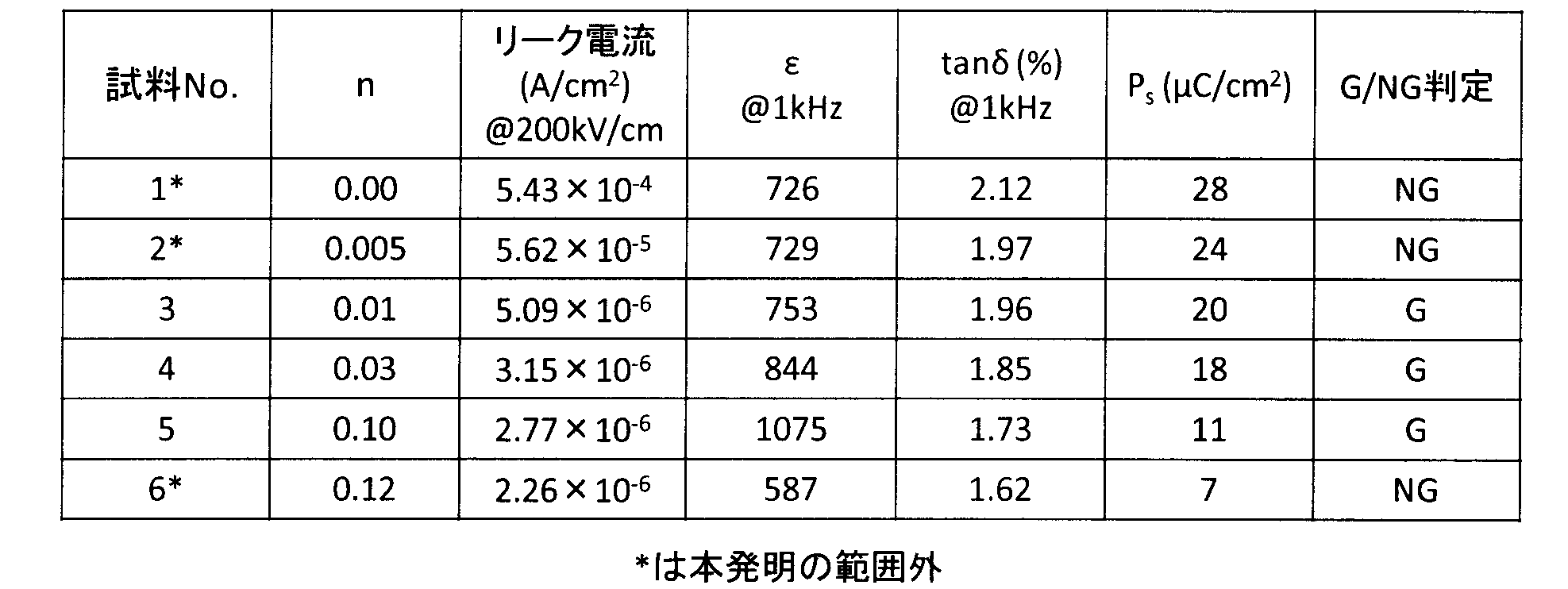
試料No.1(n=0.00、BaZrO3が含まれていないもの)および試料No.2(n=0.005)は、リーク電流が5.43×10⁻⁵A/cm2以上であるため、不良品(NG)と判定された。試料No.6(n=0.12)は、自発分極Psが10μC/cm2未満であるため、不良品(NG)と判定された。一方、試料No.3(n=0.01)、試料No.4(n=0.03)、および、試料No.5(n=0.10)は、リーク電流が5.43×10-5A/cm2以下であり、かつ自発分極Psが10μC/cm2以上であるため、良品(G)と判定された。
すなわち、試料No.2は、リーク電流が5.62×10⁻⁵A/cm2であり、試料No.1(BaZrO3が含まれていないもの)のリーク電流である5.43×10-4A/cm2とほとんど変わらなかった。しかし、試料No.3、試料No.4、試料No.5、試料No.6は、それぞれ、リーク電流が5.09×10-6A/cm2、3.15×10-6A/cm2、2.77×10-6A/cm2、2.26×10-6A/cm2であり、良好なリーク電流特性が得られた。
さらに、試料No.1~試料No.6は、それぞれ、自発分極Psが28μC/cm2、24μC/cm2、20μC/cm2、18μC/cm2、11μC/cm2、7μC/cm2であり、nが大きくなる(言い換えると,BaZrO3の割合が多くなる)につれて、自発分極Psが減少する傾向が見られた。そして、試料No.6(n=0.12)は、自発分極Psが10μC/cm2未満であり、非常に小さくなった。
以上のことから、(K0.45Na0.55)Nb0.95O3に対して、BaZrO3を0.01≦n≦0.10の範囲で固溶されたニオブ酸カリウムナトリウム系薄膜16は、優れた強誘電体特性を維持した状態で、リーク電流特性を改善できることが判る。
さらに、良品(G)と判定された試料No.3、試料No.4、試料No.5、および、比較のためにBaZrO3が含まれていない試料No.1が選択され、静電容量の温度変化が測定された。測定結果は表2に示されている。測定は、クライオスタッドを用いて、実使用温度-55℃~85℃の温度範囲に対して行われた。静電容量変化率が、測定された静電容量を使用して、(1)式より求められた。なお、C20は20℃における静電容量値であり、CTは温度Tにおける静電容量値である。
静電容量変化率={(CT-C20)/C20}×100・・・(1)
静電容量変化率={(CT-C20)/C20}×100・・・(1)
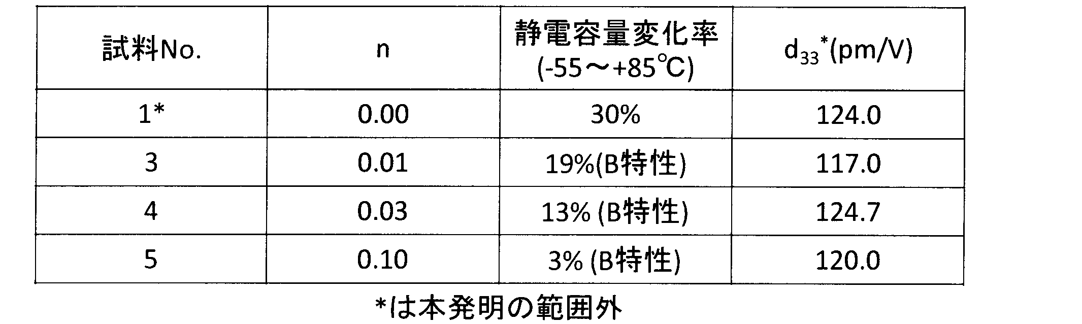
次に、試料No.1、試料No.3、試料No.4および試料No.5の電界誘起歪Zが、走査型プローブ顕微鏡「SPA400型」(商品名、エスアイアイ・ナノテクノロジー社製)を用いて測定された。測定で得られた最大印加電圧Vmaxと、その際の最大電界誘起歪Zmaxとから、Zmax/Vmaxが求められた。この値Zmax/Vmaxは、圧電定数d33
*とされる。なお、最大印加電圧Vmaxは25Vであり、測定周波数は0.5~10Hzである。得られた値の平均値が、試料の圧電定数d33
*とされる。測定結果は前記表2に示されている。
本発明の範囲外である試料No.1(n=0.00、BaZrO3が含まれていないもの)は、静電容量変化率が30%と非常に大きかった。
一方、本発明の範囲内である試料No.3(n=0.01)、試料No.4(n=0.03)および試料No.5(n=0.10)は、それぞれ、静電容量変化率が19%、13%、3%であった。すなわち、試料No.3~試料No.5の静電容量変化率は、B特性を満たし、BaZrO3の割合nが増加するに従って小さくなる。これは、バルクの(1-x)(K0.5Na0.5)NbO3-xBaZrO3系材料において、BaZrO3の割合が増加するに従って、誘電率(静電容量)の変化率が大きくなることと対照的である。
一方、試料No.3~試料No.5の圧電定数d33
*は、それぞれ、117.0pm/V、124.7pm/V、120.0pm/Vであり、試料No.1(BaZrO3が含まれていないもの)の124.0pm/Vと同等の値であった。
本第1の実施の形態は、100モルの(K0.45Na0.55)Nb0.95O3に対して、2モルのMnを含有した試料について評価した。しかし、100モルの主成分(1-n)(K0.45Na0.55)Nb0.95O3-nBaZrO3に対して、10モル以下のMnを含有した試料についても、本第1の実施の形態と同様の評価結果が得られた。
(第2の実施の形態の圧電体薄膜素子の製造)
第2の実施の形態の圧電体薄膜素子は、図2に示した前記第1の実施の形態の圧電体薄膜素子と同様の構成を有している。
第2の実施の形態の圧電体薄膜素子は、図2に示した前記第1の実施の形態の圧電体薄膜素子と同様の構成を有している。
なお、第2の実施の形態では、圧電体薄膜16である一般式(1-n)(K1-xNax)NbyO3-nBaZrO3で表示されるニオブ酸カリウムナトリウム系薄膜におけるxおよびyが変化している。
圧電体薄膜16、すなわち、ニオブ酸カリウムナトリウム(KNN)系薄膜16は、化学溶液堆積法を用いて作成される。
まず、原料であるカリウムエトキシド、ナトリウムエトキシド、ペンタエトキシニオブ、マンガンアセチルアセトナト、バリウムエトキシド(もしくはカルシウムエトキシド、もしくはストロンチウムエトキシド)、および、テトライソプロポキシジルコニウムが、モル比で(1.07-x)×0.97:(x+0.17)×0.97:y×0.97:0.02×0.97:0.03:0.03となるように準備される。ここで、本第2の実施の形態の場合、x、yは、条件式0.2≦x≦1.00、および、条件式0.8≦y≦1.15を満足する。
まず、原料であるカリウムエトキシド、ナトリウムエトキシド、ペンタエトキシニオブ、マンガンアセチルアセトナト、バリウムエトキシド(もしくはカルシウムエトキシド、もしくはストロンチウムエトキシド)、および、テトライソプロポキシジルコニウムが、モル比で(1.07-x)×0.97:(x+0.17)×0.97:y×0.97:0.02×0.97:0.03:0.03となるように準備される。ここで、本第2の実施の形態の場合、x、yは、条件式0.2≦x≦1.00、および、条件式0.8≦y≦1.15を満足する。
その後、第1の実施の形態と同様の方法で、基板12、基板12上に形成された下部電極14、下部電極14上に形成された圧電体薄膜16、および、圧電体薄膜16上に形成された上部電極18にて構成されている圧電体薄膜素子が作成される。
圧電体薄膜16は、膜厚が300nmで、組成が0.97(K1-xNax)NbyO3-0.03M1ZrO3(0.2≦x≦1.00、0.8≦y≦1.15、M1=Ca,Sr,Ba)のニオブ酸カリウムナトリウム(KNN)系薄膜である。
(第2の実施の形態の圧電体薄膜素子の評価)
表3、表4、表5および表6は、0.97(K1-xNax)NbyO3-0.03BaZrO3におけるx及びyを、0.2≦x≦1.00、0.8≦y≦1.15の範囲で変化させたときの、200kV/cmの電界におけるリーク電流、1kHzの周波数における誘電率ε及びtanδ、測定周波数10kHzで印加電界500kV/cmで測定した際の自発分極Psの値を示す(試料No.4、試料No.7~試料No.141)。なお、前記第1の実施の形態と同様に、リーク電流が5.43×10-5A/cm2以下で、かつ、自発分極Psが10μC/cm2以上の場合は、良品(G)と判定し、それ以外の場合は不良品(NG)と判定した。
表3、表4、表5および表6は、0.97(K1-xNax)NbyO3-0.03BaZrO3におけるx及びyを、0.2≦x≦1.00、0.8≦y≦1.15の範囲で変化させたときの、200kV/cmの電界におけるリーク電流、1kHzの周波数における誘電率ε及びtanδ、測定周波数10kHzで印加電界500kV/cmで測定した際の自発分極Psの値を示す(試料No.4、試料No.7~試料No.141)。なお、前記第1の実施の形態と同様に、リーク電流が5.43×10-5A/cm2以下で、かつ、自発分極Psが10μC/cm2以上の場合は、良品(G)と判定し、それ以外の場合は不良品(NG)と判定した。
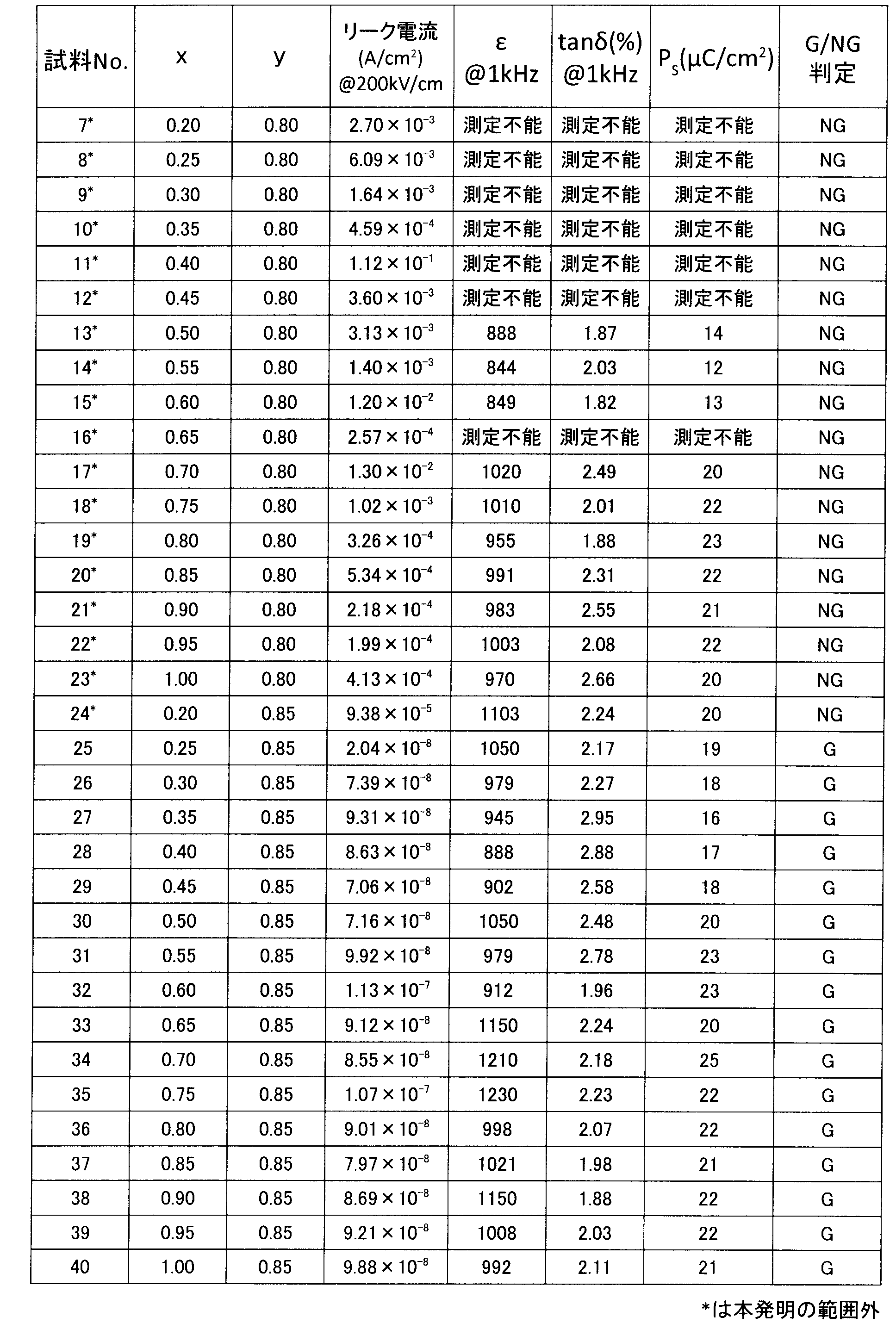
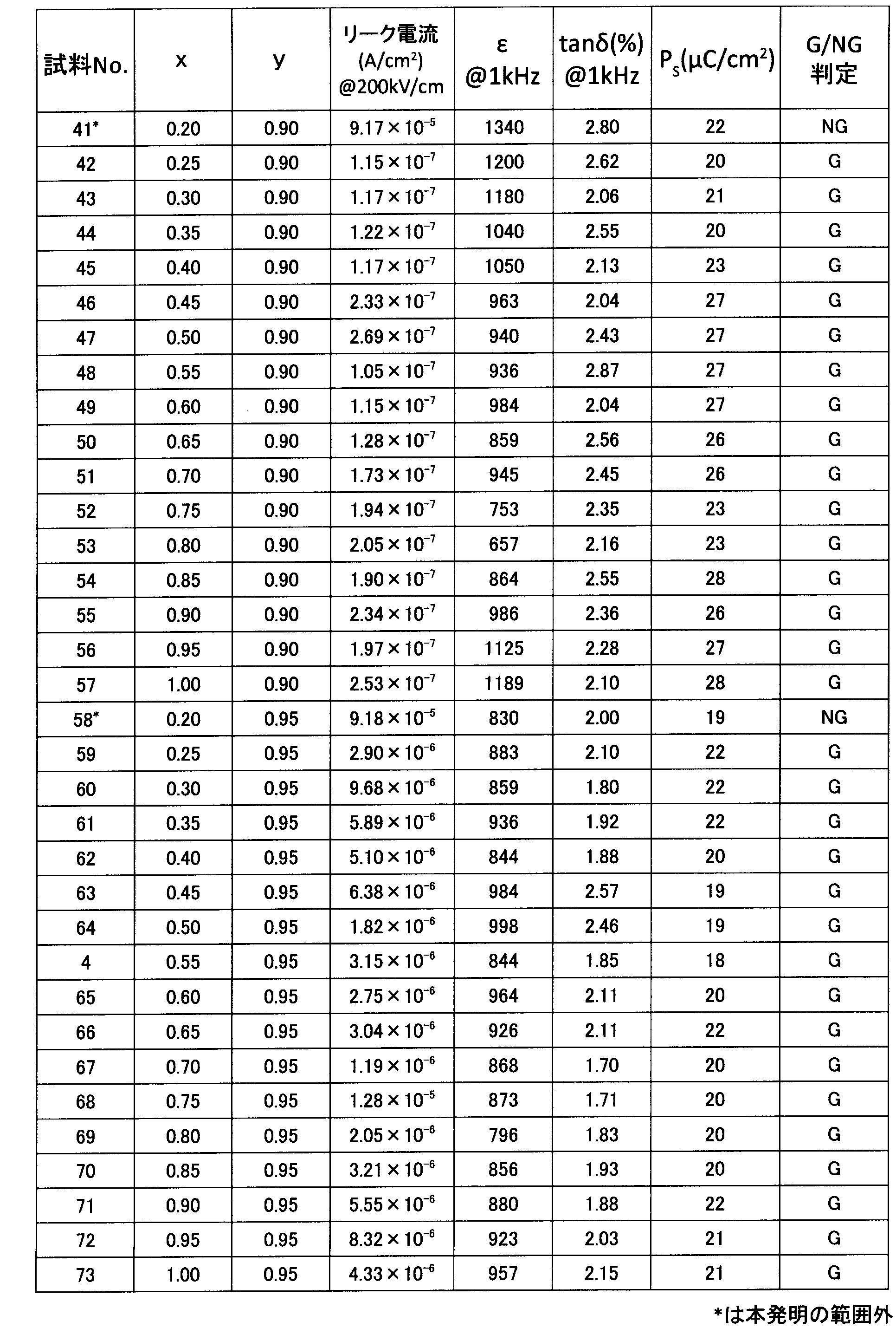
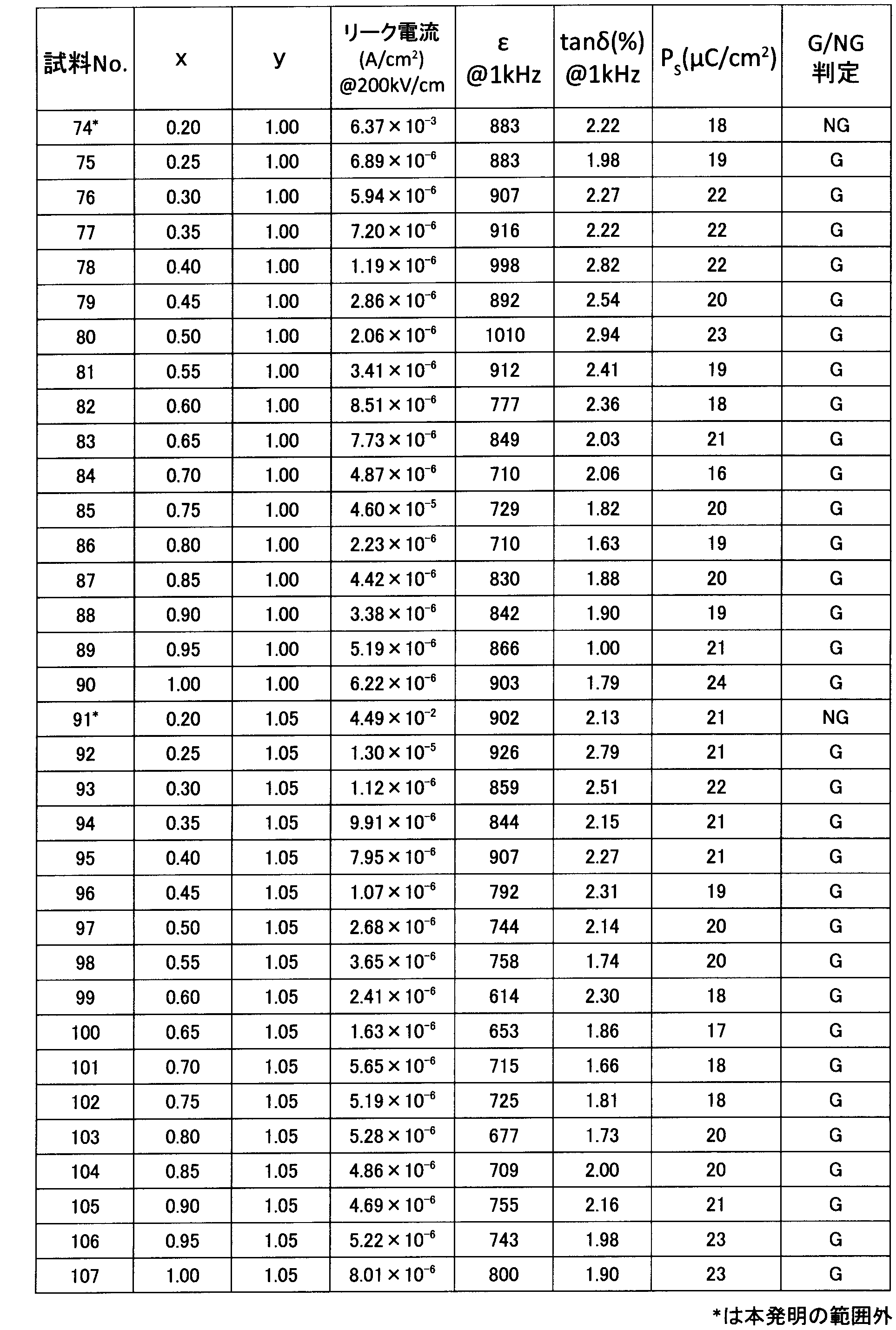

表3の試料No.7~試料No.23は、y=0.80で、xを0.20≦x≦1.00の範囲で変化させたときの試料である。これらの試料は、リーク電流が1.99×10⁻⁴A/cm2~1.12×10-1A/cm2と高く、BaZrO3を固溶させた効果が見られない。従って、試料No.7~試料No.23は、不良品(NG)と判定された。これは、Aサイトの(K1-x,Nax,Ba)とBサイトの(Nby,Zr)のモル比が、化学量論的な組成から大きく外れているためである。
試料No.24~試料No.40は、y=0.85で、xを0.20≦x≦1.00の範囲で変化させたときの試料である。その中で、x=0.20の試料(試料No.24)は、リーク電流が9.38×10⁻⁵A/cm2である。この値は、BaZrO3が含まれていない試料No.1と比較して、殆んど変化が見られず、不良品(NG)と判定された。
一方、0.25≦x≦1.00の試料(試料No.25~試料No.40)は、リーク電流が2.04×10⁻⁸A/cm2~1.13×10-7A/cm2である。これらの値は、BaZrO3が含まれていない試料No.1と比較して、大幅なリーク電流の向上が見られた。さらに、自発分極Psは16~25μC/cm2であり、強誘電体特性も維持していた。従って、0.25≦x≦1.00の試料(試料No.25~試料No.40)は、良品(G)と判定された。
表4の試料No.41~試料No.57は、y=0.90で、xを0.20≦x≦1.00の範囲で変化させたときの試料である。その中で、x=0.20の試料(試料No.41)は、リーク電流が9.17×10⁻⁵A/cm2である。この値は、BaZrO3が含まれていない試料No.1と比較して、殆んど変化が見られず、不良品(NG)と判定された。
一方、0.25≦x≦1.00の試料(試料No.42~試料No.57)は、リーク電流が1.05×10⁻⁷A/cm2~2.69×10-7A/cm2である。これらの値は、BaZrO3が含まれていない試料No.1と比較して、大幅なリーク電流の向上が見られた。さらに、自発分極Psは20~27μC/cm2であり、強誘電体特性も維持していた。従って、0.25≦x≦1.00の試料(試料No.42~試料No.57)は、良品(G)と判定された。
表4の試料No.4および試料No.58~試料No.73は、y=0.95で、xを0.20≦x≦1.00の範囲で変化させたときの試料である。その中で、x=0.20の試料(試料No.58)は、リーク電流が9.18×10⁻⁵A/cm2である。この値は、BaZrO3が含まれていない試料No.1と比較して、殆んど変化が見られない、もしくは、悪化しているため、不良品(NG)と判定された。
一方、0.25≦x≦1.00の試料(試料No.4および試料No.59~試料No.73)は、リーク電流が1.19×10⁻⁶A/cm2~9.68×10-6A/cm2である。これらの値は、BaZrO3が含まれていない試料No.1と比較して、大幅なリーク電流の向上が見られた。さらに、自発分極Psは18~22μC/cm2であり、強誘電体特性も維持していた。従って、0.25≦x≦1.00の試料(試料No.4および試料No.59~試料No.73)は、良品(G)と判定された。
表5の試料No.74~試料No.90は、y=1.00で、xを0.20≦x≦1.00の範囲で変化させたときの試料である。その中で、x=0.20の試料(試料No.74)は、リーク電流が6.37×10⁻³A/cm2である。この値は、BaZrO3が含まれていない試料No.1と比較して、殆んど変化が見られず、不良品(NG)と判定された。
一方、0.25≦x≦1.00の試料(試料No.75~試料No.90)は、リーク電流が1.19×10⁻⁶A/cm2~8.51×10-6A/cm2である。これらの値は、BaZrO3が含まれていない試料No.1と比較して、大幅なリーク電流の向上が見られた。さらに、自発分極Psは16~24μC/cm2と強誘電体特性も維持していた。従って、0.25≦x≦1.00の試料(試料No.75~試料No.90)は、良品(G)と判定された。
表5の試料No.91~試料No.107は、y=1.05で、xを0.20≦x≦1.00の範囲で変化させたときの試料である。その中で、x=0.20の試料(試料No.91)は、リーク電流が4.49×10⁻²A/cm2である。この値は、BaZrO3が含まれていない試料No.1と比較して、悪化しており、不良品(NG)と判定された。
一方、0.25≦x≦1.00の試料(試料No.92~試料No.107)は、リーク電流が1.07×10⁻⁶A/cm2~5.19×10-6A/cm2である。これらの値は、BaZrO3が含まれていない試料No.1と比較して、大幅なリーク電流の向上が見られた。さらに、自発分極Psは17~23μC/cm2と強誘電体特性も維持していた。従って、0.25≦x≦1.00の試料(試料No.92~試料No.107)は、良品(G)と判定された。
表6の試料No.108~試料No.124は、y=1.10で、xを0.20≦x≦1.00の範囲で変化させたときの試料である。その中で、x=0.20の試料(試料No.108)は、リーク電流が8.86×10⁻⁴A/cm2である。この値は、BaZrO3が含まれていない試料No.1と比較して、殆んど変化が見られない、もしくは、悪化しているため、不良品(NG)と判定された。
一方、0.25≦x≦1.00の試料(試料No.109~試料No.124)は、リーク電流が2.18×10⁻⁶A/cm2~3.20×10-5A/cm2である。これらの値は、BaZrO3が含まれていない試料No.1と比較して、大幅なリーク電流の向上が見られた。さらに、自発分極Psは15~21μC/cm2と強誘電体特性も維持していた。従って、0.25≦x≦1.00の試料(試料No.109~試料No.124)は、良品(G)と判定された。
試料No.125~試料No.141は、y=1.15で、xを0.20≦x≦1.00の範囲で変化させたときの試料である。これらの試料は、リーク電流が8.18×10⁻⁵A/cm2~1.76×10-1A/cm2と高く、BaZrO3を固溶させた効果が見られない。従って、試料No.125~試料No.141は、不良品(NG)と判定された。これは、Aサイトの(K1-x,Nax,Ba)とBサイトの(Nby,Zr)のモル比が、化学量論的な組成から大きく外れているためである。
また、良品(G)と判定された試料は、全てtanδが3%以下であり、非常に低い。従って、高品質なニオブ酸カリウムナトリウム系薄膜16が作成されていることが判る。
さらに、上記の良品/不良品(G/NG)判定で、良品(G)と判定された試料(試料No.4、試料No.25~試料No.40など)の電界誘起歪Zが、走査型プローブ顕微鏡「SPA400型」(商品名、エスアイアイ・ナノテクノロジー社製)を用いて測定された。測定で得られた最大印加電圧Vmaxと、その際の最大電界誘起歪Zmaxとから、Zmax/Vmaxが求められた。この値Zmax/Vmaxは、圧電定数d33
*とされる。なお、最大印加電圧Vmaxは25Vであり、測定周波数は0.5~10Hzである。得られた値の平均値が、試料の圧電定数d33
*とされる。測定結果は表7、表8および表9に示されている。
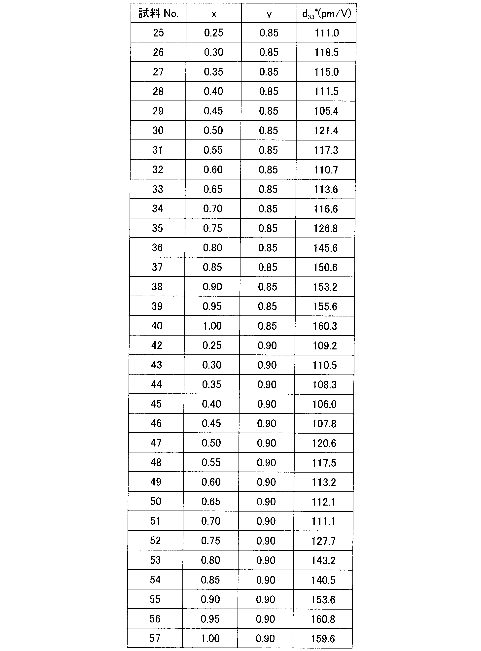
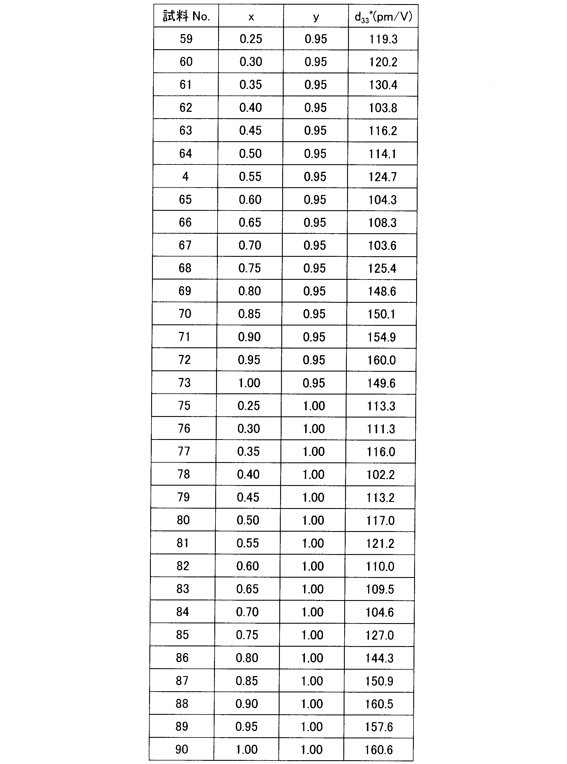

表7~表9より、圧電定数d33
*は、100.5~160.8pm/Vであり、試料No.1(BaZrO3が含まれていないもの)の124.0pm/Vと同等以上の数値が得られることが判る。
特に、xの範囲が0.80≦x≦1.00の試料(試料No.36~試料No.40など)は、圧電定数d33
*が140.5~160.8pm/Vであり、試料No.1(BaZrO3が含まれていないもの)の124.0pm/Vと比較して、非常に大きな数値であることが判る。
表10は、x=0.90、y=0.95、n=0.03としたときの、0.97(K0.1Na0.9)Nb0.95O3-0.03M1ZrO3(M1=Ca,Sr)において、200kV/cmの電界におけるリーク電流、1kHzの周波数における誘電率ε及びtanδ、測定周波数10kHzで印加電界500kV/cmで測定した際の自発分極Ps及び圧電定数d33
*の値を示す(試料No.142,143)。
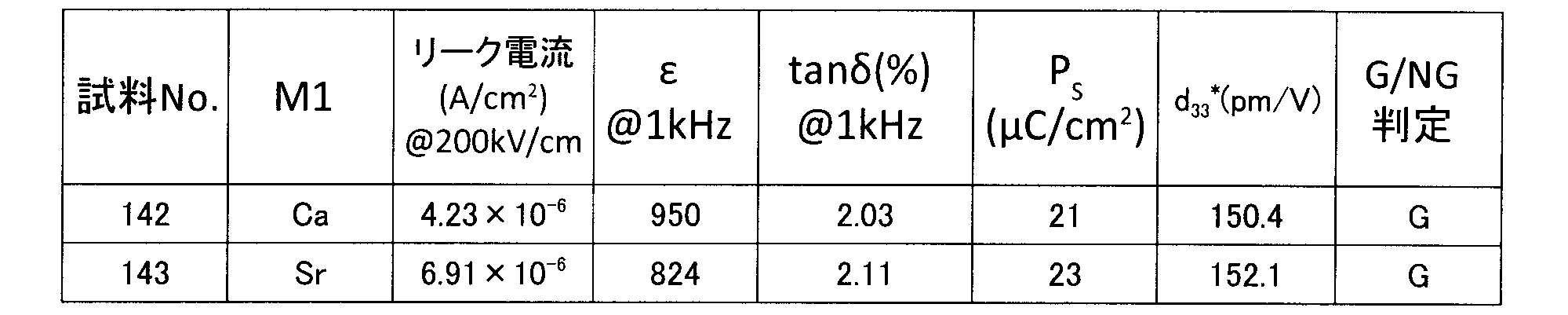
表10より、M1=Caの試料(試料No.142)は、リーク電流が4.23×10⁻⁶A/cm2であり、低かった。さらに、自発分極Psは21μC/cm2であり、強誘電性も維持していた。従って、M1=Caの試料(試料No.142)は、良品(G)と判定された。
また、M1=Srの試料(試料No.143)についても、リーク電流が6.91×10⁻⁶A/cm2であり、低かった。さらに、自発分極Psは23μC/cm2であり、強誘電性も維持していた。従って、M1=Srの試料(試料No.143)は、良品(G)と判定された。
なお、これらのM1=Ca,Srの試料(試料No.142,143)の圧電定数d33
*は、それぞれ、150.4pm/V及び152.1pm/Vであり、M1ZrO3(M1=Ca,Sr)が含まれていない試料と比較して、圧電定数d33
*の向上が見られた。
本第2の実施の形態は、100モルの(K1-xNax)NbyO3に対して、2モルのMnを含有した試料について評価した。しかし、100モルの主成分0.97(K1-xNax)NbyO3-0.03M1ZrO3(M1=Ca、Sr、Ba)に対して、10モル以下のMnを含有した試料についても、本第2の実施の形態と同様の評価結果が得られた。
従って、本第2の実施の形態における評価結果から、圧電体薄膜16である一般式(1-n)(K1-xNax)NbyO3-nM1ZrO3(M1=Ca、Sr、Ba)で表示されるニオブ酸カリウムナトリウム系薄膜において、0.25≦x≦1.00、0.85≦y≦1.10とすることで、リーク電流特性、強誘電体特性及び圧電体特性に優れた圧電体薄膜素子を得られることが明らかとなった。
図3は、試料No.4の強誘電体ヒステリシス曲線を示す。ニオブ酸カリウムナトリウムにBaZrO3を固溶させることによって、100kV/cm以上の電界におけるリーク電流特性が向上し、最大印加電圧1MV/cm、測定周波数100Hzにおいても良好な強誘電体ヒステリシス曲線を示すことが判る。
このように本発明に係る圧電体薄膜素子において、圧電体薄膜の一般式(1-n)(K1-xNax)NbyO3-nM1ZrO3(M1=Ca、Sr、Ba)で表示されるニオブ酸カリウムナトリウム系薄膜であって、x、yおよびnの範囲が、それぞれ、0.25≦x≦1.00、0.85≦y≦1.10および0.01≦n≦0.10とすることにより、リーク電流特性、強誘電体特性および圧電体特性に優れた圧電体薄膜素子が得られる。さらに、強誘電体薄膜素子や圧電体薄膜素子の使用の際に問題になる静電容量の温度変化が、抑えられる。
(第3の実施の形態の圧電体薄膜素子の製造)
第3の実施の形態の圧電体薄膜素子は、図2に示した前記第1の実施の形態の圧電体薄膜素子と同様の構成を有している。
第3の実施の形態の圧電体薄膜素子は、図2に示した前記第1の実施の形態の圧電体薄膜素子と同様の構成を有している。
なお、第3の実施の形態では、圧電体薄膜16である一般式(1-n)(K1-xNax)NbyO3-nBaSnO3で表示されるニオブ酸カリウムナトリウム系薄膜におけるBaSnO3の含有量が変化している。
圧電体薄膜16、すなわち、ニオブ酸カリウムナトリウム(KNN)系薄膜16は、化学溶液堆積法を用いて作成される。
まず、原料であるカリウムエトキシド、ナトリウムエトキシド、ペンタエトキシニオブ、マンガンアセチルアセトナト、バリウムエトキシド、および、テトライソプロポキシスズが、モル比で0.52×(1-n):0.72×(1-n):0.95×(1-n):0.02×(1-n):n:nとなるように準備される。ここで、本第3の実施の形態の場合、nは、0.00、0.005、0.01、0.03、0.05、0.1、0.12の7種類が選択される。
次に、原料のカリウムエトキシド、ナトリウムエトキシド、ペンタエトキシニオブ、マンガンアセチルアセトナト、バリウムエトキシド、および、テトライソプロポキシスズが、グローブボックスの中で、2-メトキシエタノール溶媒に混合される。
次に、その混合溶液は、窒素雰囲気中において、125℃で16時間還流されることによって、濃度が0.3Mのニオブ酸カリウムナトリウム(KNN)系前駆体溶液(化学溶液堆積用溶液とも称される)とされる。
なお、この前駆体溶液に、アルコキシドの安定化剤として一般的に用いられている有機物を添加しても良い。
有機物の種類としては、例えば、無水カルボン酸類、ジカルボン酸モノエステル類、β-ジケトン類、グリコール類、アミン類などが挙げられるが、これに限定されるものではない。また、有機物は還流前に添加しても良いし、還流後に添加しても良い。
なお、この前駆体溶液に、アルコキシドの安定化剤として一般的に用いられている有機物を添加しても良い。
有機物の種類としては、例えば、無水カルボン酸類、ジカルボン酸モノエステル類、β-ジケトン類、グリコール類、アミン類などが挙げられるが、これに限定されるものではない。また、有機物は還流前に添加しても良いし、還流後に添加しても良い。
一方、下部電極14が、Si基板12上に、マグネトロンDCスパッタリング法によって形成される。下部電極14の材料としては、Ptなどが用いられる。
スパッタリング条件は、スパッタ出力が100W、スパッタ時間が5分、基板12の温度が300℃、真空度が5ミリtorrである。
次に、ニオブ酸カリウムナトリウム系前駆体溶液が、乾燥ガス中において、下部電極14上にスピンコート塗布される。
次に、第一熱処理(予備熱処理または乾燥処理)が実行される。すなわち、下部電極14上に塗布されたニオブ酸カリウムナトリウム系前駆体溶液が、予め350℃の温度に加熱されたホットプレートを用いて、急速に昇温され、350℃で3分間乾燥される。
次に、第二熱処理(本熱処理または焼成処理)が実行される。すなわち、乾燥されたニオブ酸カリウムナトリウム系前駆体膜は、350℃~750℃の温度範囲(還流により形成される錯体が急激に分解する温度500℃付近を含む)において、5℃/分以下の昇温速度で昇温され、750℃の温度で10分間焼成される。こうして、ニオブ酸カリウムナトリウム系層16aが形成される。前記工程1回で形成されるニオブ酸カリウムナトリウム系層16aの厚みは、30nmである。
さらに、ニオブ酸カリウムナトリウム系層16aを形成する前記工程が、10回繰り返されて、膜厚が300nmの(1-n)(K0.45Na0.55)Nb0.95O3-nBaSnO3の組成を有するニオブ酸カリウムナトリウム系薄膜16が形成される。
次に、上部電極18が、ニオブ酸カリウムナトリウム系薄膜16上に、マグネトロンDCスパッタリング法によって形成される。上部電極18の材料としては、Ptなどが用いられる。
スパッタリング条件は、スパッタ出力が100W、スパッタ時間が5分、基板12の温度が150℃、真空度が5ミリtorrである。
こうして、圧電体薄膜素子が得られる。
こうして、圧電体薄膜素子が得られる。
ニオブ酸カリウムナトリウム系薄膜16の組成は、誘導結合プラズマ(Inductively Coupled Plasma)組成分析によって、目標通りであることが確認された。
(第3の実施の形態の圧電体薄膜素子の評価)
表11は、BaSnO3の割合nを、0.00(試料No.201)、0.005(試料No.202)、0.01(試料No.203)、0.03(試料No.204)、0.10(試料No.205)、0.12(試料No.206)と変化させた場合の、圧電体薄膜素子の電気特性を示す。電気特性の項目は、絶縁性、誘電率ε、tanδおよび強誘電体特性である。
表11は、BaSnO3の割合nを、0.00(試料No.201)、0.005(試料No.202)、0.01(試料No.203)、0.03(試料No.204)、0.10(試料No.205)、0.12(試料No.206)と変化させた場合の、圧電体薄膜素子の電気特性を示す。電気特性の項目は、絶縁性、誘電率ε、tanδおよび強誘電体特性である。

試料No.201(n=0.00、BaSnO3が含まれていないもの)および試料No.202(n=0.005)は、リーク電流が5.43×10⁻⁵A/cm2以上であるため、不良品(NG)と判定された。試料No.206(n=0.12)は、自発分極Psが10μC/cm2未満であるため、不良品(NG)と判定された。一方、試料No.203(n=0.01)、試料No.204(n=0.03)、および、試料No.205(n=0.10)は、リーク電流が5.43×10-5A/cm2以下であり、かつ自発分極Psが10μC/cm2以上であるため、良品(G)と判定された。
すなわち、試料No.202は、リーク電流が8.22×10⁻⁵A/cm2であり、試料No.201(BaSnO3が含まれていないもの)のリーク電流である5.43×10-4A/cm2とほとんど変わらなかった。しかし、試料No.203、試料No.204、試料No.205、試料No.206は、それぞれ、リーク電流が3.26×10-6A/cm2、1.17×10-7A/cm2、2.38×10-7A/cm2、1.98×10-7A/cm2であり、良好なリーク電流特性が得られた。
さらに、試料No.201~試料No.206は、それぞれ、自発分極Psが28μC/cm2、23μC/cm2、18μC/cm2、14μC/cm2、11μC/cm2、8μC/cm2であり、nが大きくなる(言い換えると,BaSnO3の割合が多くなる)につれて、自発分極Psが減少する傾向が見られた。そして、試料No.206(n=0.12)は、自発分極Psが10μC/cm2未満であり、非常に小さくなった。
以上のことから、(K0.45Na0.55)Nb0.95O3に対して、BaSnO3が0.01≦n≦0.10の範囲で固溶されたニオブ酸カリウムナトリウム系薄膜16は、優れた強誘電体特性を維持した状態で、リーク電流特性を改善できることが判る。
さらに、試料No.201~試料No.206の圧電定数d33
*が前記第1の実施の形態と同様にして求められた。測定結果は表12に示されている。
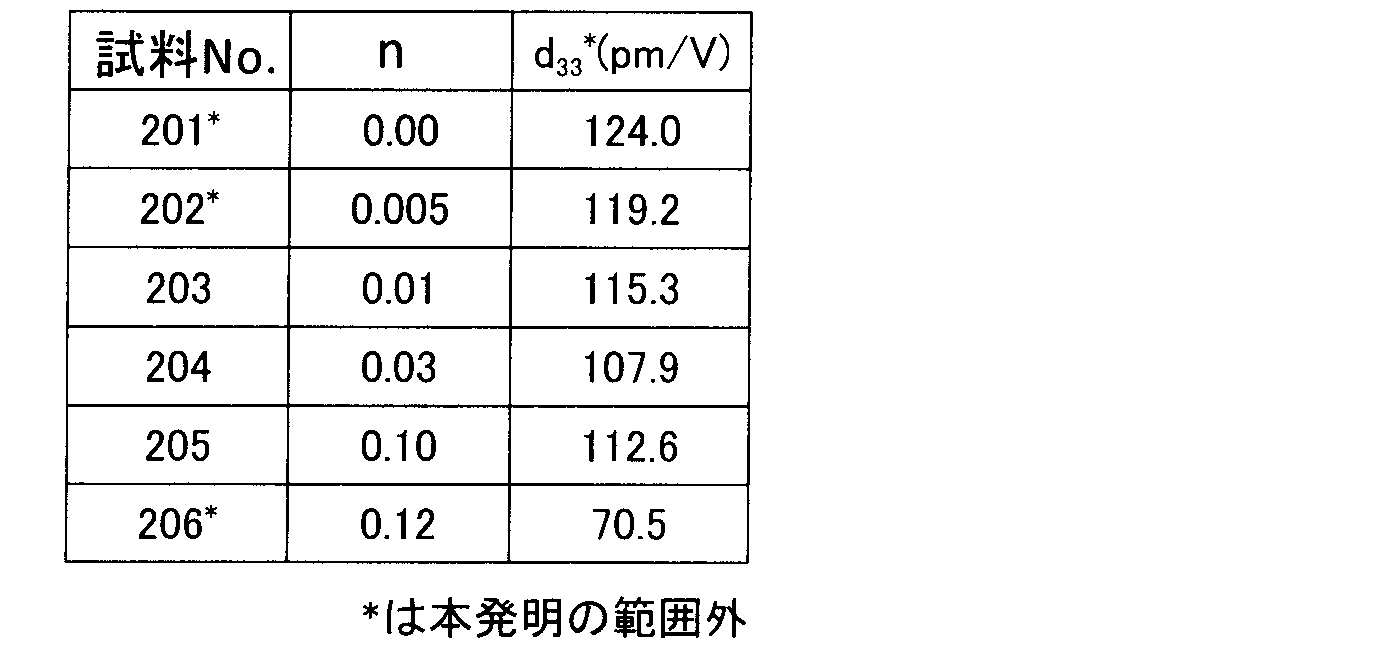
試料No.202~試料No.205の圧電定数d33
*は、それぞれ、119.2pm/V、115.3pm/V、107.9pm/V、112.6pm/Vであり、試料No.201(BaSnO3が含まれていないもの)の124.0pm/Vと同等の値であった。一方、試料No.206(n=0.12)の圧電定数d33
*は、70.5pm/Vと、急激に小さくなった。これは、自発分極Psの値が10μC/cm2以下と、非常に小さくなっているためである。
本第3の実施の形態は、100モルの(K0.45Na0.55)Nb0.95O3に対して、2モルのMnを含有した試料について評価した。しかし、100モルの主成分(1-n)(K0.45Na0.55)Nb0.95O3-nBaSnO3に対して、10モル以下のMnを含有した試料についても、本第3の実施の形態と同様の評価結果が得られた。
(第4の実施の形態の圧電体薄膜素子の製造)
第4の実施の形態の圧電体薄膜素子は、図2に示した前記第1の実施の形態の圧電体薄膜素子と同様の構成を有している。
第4の実施の形態の圧電体薄膜素子は、図2に示した前記第1の実施の形態の圧電体薄膜素子と同様の構成を有している。
なお、第4の実施の形態では、圧電体薄膜16である一般式(1-n)(K1-xNax)NbyO3-nBaSnO3で表示されるニオブ酸カリウムナトリウム系薄膜におけるxおよびyが変化している。
圧電体薄膜16、すなわち、ニオブ酸カリウムナトリウム(KNN)系薄膜16は、化学溶液堆積法を用いて作成される。
まず、原料であるカリウムエトキシド、ナトリウムエトキシド、ペンタエトキシニオブ、マンガンアセチルアセトナト、バリウムエトキシド、および、テトライソプロポキシスズが、モル比で(1.07-x)×0.97:(x+0.17)×0.97:y×0.97:0.02×0.97:0.03:0.03となるように準備される。ここで、本第4の実施の形態の場合、x、yは、条件式0.2≦x≦1.00、および、条件式0.85≦y≦1.10を満足する。
まず、原料であるカリウムエトキシド、ナトリウムエトキシド、ペンタエトキシニオブ、マンガンアセチルアセトナト、バリウムエトキシド、および、テトライソプロポキシスズが、モル比で(1.07-x)×0.97:(x+0.17)×0.97:y×0.97:0.02×0.97:0.03:0.03となるように準備される。ここで、本第4の実施の形態の場合、x、yは、条件式0.2≦x≦1.00、および、条件式0.85≦y≦1.10を満足する。
その後、第3の実施の形態と同様の方法で、基板12、基板12上に形成された下部電極14、下部電極14上に形成された圧電体薄膜16、および、圧電体薄膜16上に形成された上部電極18にて構成されている圧電体薄膜素子が作成される。
圧電体薄膜16は、膜厚が300nmで、組成が0.97(K1-xNax)NbyO3-0.03BaSnO3(0.2≦x≦1.00、0.85≦y≦1.10)のニオブ酸カリウムナトリウム(KNN)系薄膜である。
(第4の実施の形態の圧電体薄膜素子の評価)
表13、表14および表15は、0.97(K1-xNax)NbyO3-0.03BaSnO3におけるx及びyを、0.2≦x≦1.00、0.85≦y≦1.10の範囲で変化させたときの、200kV/cmの電界におけるリーク電流、1kHzの周波数における誘電率ε及びtanδ、測定周波数10kHzで印加電界500kV/cmで測定した際の自発分極Psの値を示す(試料No.204、試料No.207~試料No.307)。なお、前記第3の実施の形態と同様に、リーク電流が5.43×10-5A/cm2以下で、かつ、自発分極Psが10μC/cm2以上の場合は、良品(G)と判定し、それ以外の場合は不良品(NG)と判定した。
表13、表14および表15は、0.97(K1-xNax)NbyO3-0.03BaSnO3におけるx及びyを、0.2≦x≦1.00、0.85≦y≦1.10の範囲で変化させたときの、200kV/cmの電界におけるリーク電流、1kHzの周波数における誘電率ε及びtanδ、測定周波数10kHzで印加電界500kV/cmで測定した際の自発分極Psの値を示す(試料No.204、試料No.207~試料No.307)。なお、前記第3の実施の形態と同様に、リーク電流が5.43×10-5A/cm2以下で、かつ、自発分極Psが10μC/cm2以上の場合は、良品(G)と判定し、それ以外の場合は不良品(NG)と判定した。
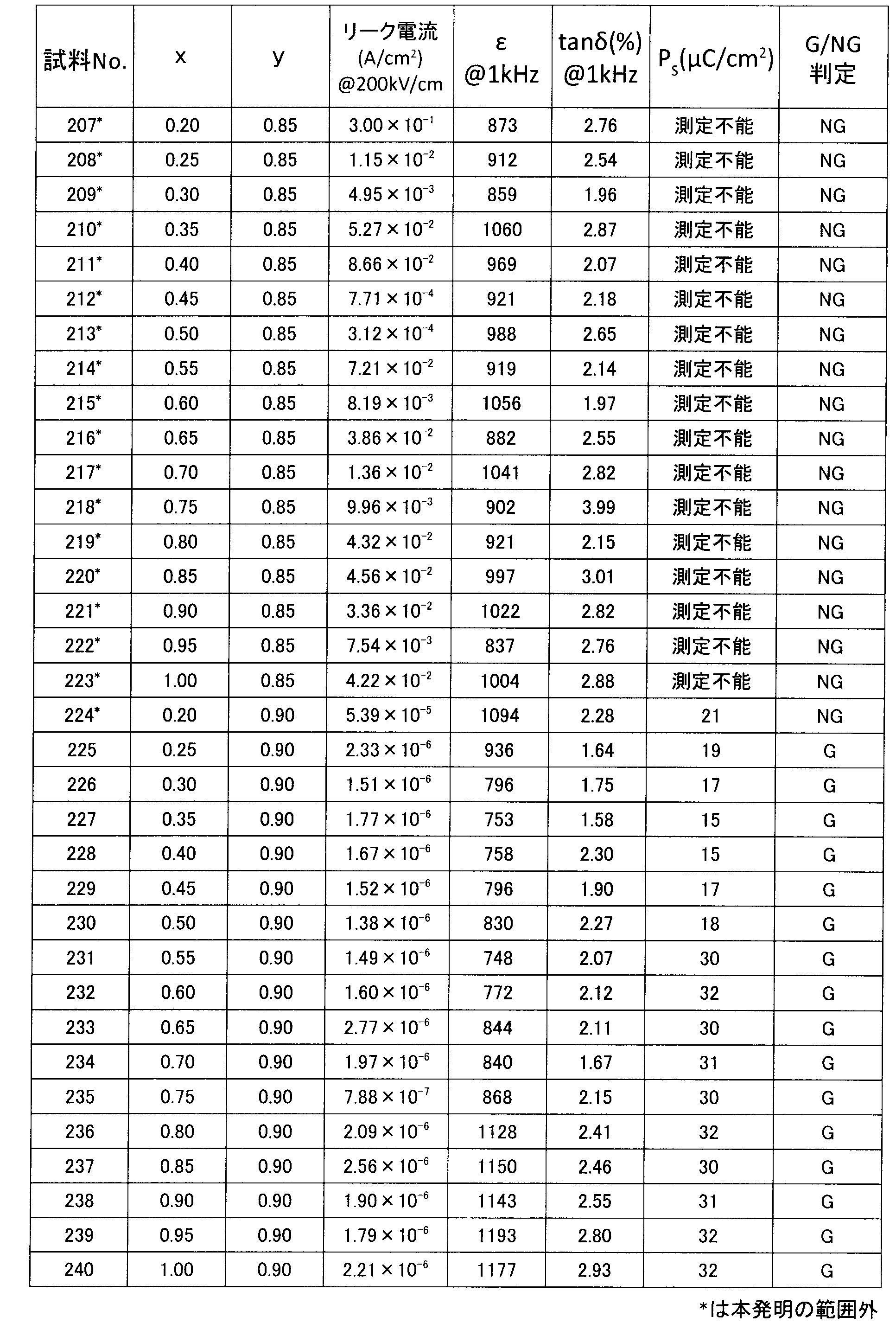

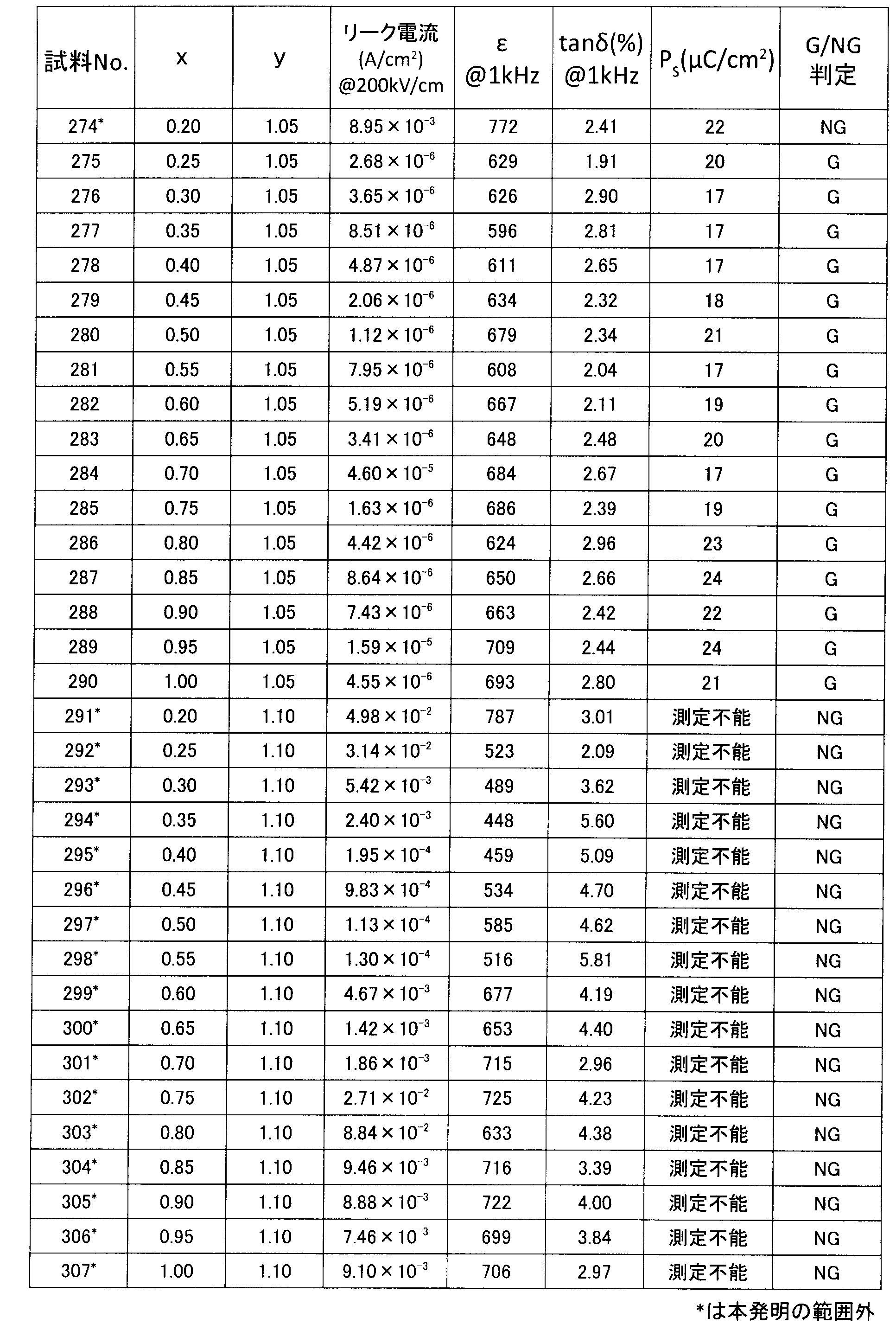
表13の試料No.207~試料No.223は、y=0.85で、xを0.20≦x≦1.00の範囲で変化させたときの試料である。これらの試料は、リーク電流が3.12×10⁻⁴A/cm2~3.00×10-1A/cm2と高く、BaSnO3を固溶させた効果が見られない。従って、試料No.207~試料No.223は、不良品(NG)と判定された。これは、Aサイトの(K1-x,Nax,Ba)とBサイトの(Nby,Sn)のモル比が、化学量論的な組成から大きく外れているためである。
試料No.224~試料No.240は、y=0.90で、xを0.20≦x≦1.00の範囲で変化させたときの試料である。その中で、x=0.20の試料(試料No.224)は、リーク電流が6.39×10⁻⁵A/cm2である。この値は、BaSnO3が含まれていない試料No.201と比較して、殆んど変化が見られず、不良品(NG)と判定された。
一方、0.25≦x≦1.00の試料(試料No.225~試料No.240)は、リーク電流が7.88×10⁻⁷A/cm2~2.77×10-6A/cm2である。これらの値は、BaSnO3が含まれていない試料No.201と比較して、大幅なリーク電流の向上が見られた。さらに、自発分極Psは15~32μC/cm2であり、強誘電体特性も維持していた。従って、0.25≦x≦1.00の試料(試料No.225~試料No.240)は、良品(G)と判定された。
表14の試料No.204および試料No.241~試料No.256は、y=0.95で、xを0.20≦x≦1.00の範囲で変化させたときの試料である。その中で、x=0.20の試料(試料No.241)は、リーク電流が6.56×10⁻³A/cm2である。この値は、BaSnO3が含まれていない試料No.201と比較して、悪化しているため、不良品(NG)と判定された。
一方、0.25≦x≦1.00の試料(試料No.204および試料No.242~試料No.256)は、リーク電流が1.17×10⁻⁷A/cm2~8.47×10-6A/cm2である。これらの値は、BaSnO3が含まれていない試料No.201と比較して、大幅なリーク電流の向上が見られた。さらに、自発分極Psは14~25μC/cm2であり、強誘電体特性も維持していた。従って、0.25≦x≦1.00の試料(試料No.204および試料No.242~試料No.256)は、良品(G)と判定された。
試料No.257~試料No.273は、y=1.00で、xを0.20≦x≦1.00の範囲で変化させたときの試料である。その中で、x=0.20の試料(試料No.257)は、リーク電流が2.64×10⁻³A/cm2である。この値は、BaSnO3が含まれていない試料No.201と比較して、悪化しているため、不良品(NG)と判定された。
一方、0.25≦x≦1.00の試料(試料No.258~試料No.273)は、リーク電流が1.07×10⁻⁶A/cm2~1.30×10-5A/cm2である。これらの値は、BaSnO3が含まれていない試料No.201と比較して、大幅なリーク電流の向上が見られた。さらに、自発分極Psは15~26μC/cm2であり、強誘電体特性も維持していた。従って、0.25≦x≦1.00の試料(試料No.258~試料No.273)は、良品(G)と判定された。
表15の試料No.274~試料No.290は、y=1.05で、xを0.20≦x≦1.00の範囲で変化させたときの試料である。その中で、x=0.20の試料(試料No.274)は、リーク電流が8.95×10⁻³A/cm2である。この値は、BaSnO3が含まれていない試料No.201と比較して、悪化しているため、不良品(NG)と判定された。
一方、0.25≦x≦1.00の試料(試料No.275~試料No.290)は、リーク電流が1.12×10⁻⁶A/cm2~4.60×10-5A/cm2である。これらの値は、BaSnO3が含まれていない試料No.201と比較して、大幅なリーク電流の向上が見られた。さらに、自発分極Psは17~24μC/cm2と強誘電体特性も維持していた。従って、0.25≦x≦1.00の試料(試料No.275~試料No.290)は、良品(G)と判定された。
試料No.291~試料No.307は、y=1.10で、xを0.20≦x≦1.00の範囲で変化させたときの試料である。これらの試料は、リーク電流が1.13×10⁻⁴A/cm2~8.84×10-2A/cm2と高く、BaSnO3を固溶させた効果が見られない。従って、試料No.291~試料No.307は、不良品(NG)と判定された。これは、Aサイトの(K1-x,Nax,Ba)とBサイトの(Nby,Sn)のモル比が、化学量論的な組成から大きく外れているためである。
また、良品(G)と判定された試料は、全てtanδが3%以下であり、非常に低い。従って、高品質なニオブ酸カリウムナトリウム系薄膜16が作成されていることが判る。
さらに、上記の良品/不良品(G/NG)判定で、良品(G)と判定された試料(試料No.204、試料No.225~試料No.240など)の圧電定数d33
*が、前記第2の実施の形態と同様にして求められた。測定結果は表16および表17に示されている。

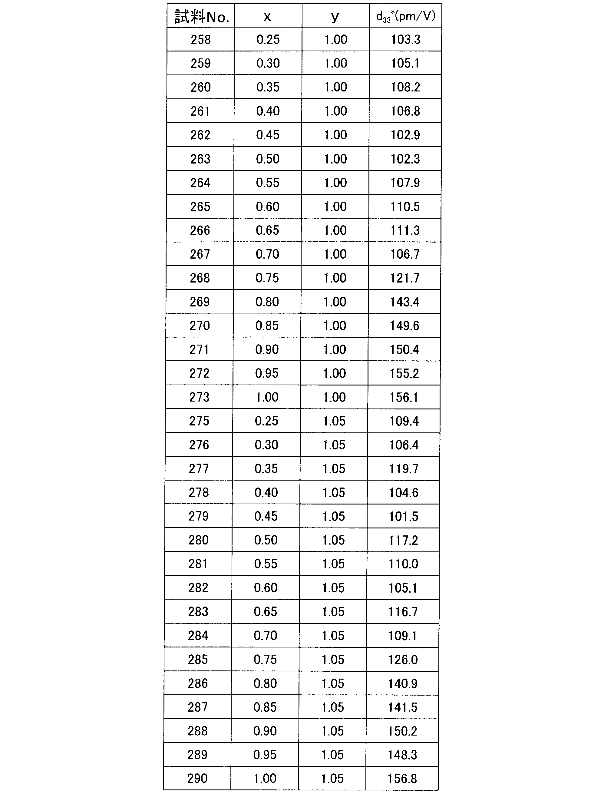
表16および表17より、圧電定数d33
*は、100.5~158.2pm/Vであり、試料No.201(BaSnrO3が含まれていないもの)の124.0pm/Vと殆んど変わらないことが判る。これは、自発分極Psの値が10μC/cm2以上と、大きな値を示しているためである。
特に、xの範囲が0.80≦x≦1.00の試料(試料No.236~試料No.240など)は、圧電定数d33
*が139.7~158.2pm/Vであり、試料No.201(BaSnO3が含まれていないもの)の124.0pm/Vと比較して、非常に大きな数値であることが判る。
表18は、x=0.90、y=0.95、n=0.03としたときの、0.97(K0.1Na0.9)Nb0.95O3-0.03M1SnO3(M1=Ca,Sr)において、200kV/cmの電界におけるリーク電流、1kHzの周波数における誘電率ε及びtanδ、測定周波数10kHzで印加電界500kV/cmで測定した際の自発分極Ps及び圧電定数d33
*の値を示す(試料No.308,309)。

表18より、M1=Caの試料(試料No.308)は、リーク電流が3.22×10⁻⁶A/cm2であり、低かった。さらに、自発分極Psは20μC/cm2であり、強誘電性も維持していた。従って、M1=Caの試料(試料No.308)は、良品(G)と判定された。
また、M1=Srの試料(試料No.309)についても、リーク電流が4.19×10⁻⁶A/cm2であり、低かった。さらに、自発分極Psは21μC/cm2であり、強誘電性も維持していた。従って、M1=Srの試料(試料No.309)は、良品(G)と判定された。
なお、これらのM1=Ca,Srの試料(試料No.308,309)の圧電定数d33
*は、それぞれ、151.4pm/V及び148.3pm/Vであり、M1SnO3(M1=Ca,Sr)が含まれていない試料と比較して、圧電定数d33
*の向上が見られた。
本第4の実施の形態は、100モルの(K1-xNax)NbyO3に対して、2モルのMnを含有した試料について評価した。しかし、100モルの主成分0.97(K1-xNax)NbyO3-0.03M1SnO3(M1=Ca,Sr,Ba)に対して、10モル以下のMnを含有した試料についても、本第4の実施の形態と同様の評価結果が得られた。
従って、本第4の実施の形態における評価結果から、圧電体薄膜16である一般式(1-n)(K1-xNax)NbyO3-nM1SnO3(M1=Ca,Sr,Ba)で表示されるニオブ酸カリウムナトリウム系薄膜において、0.25≦x≦1.00、0.90≦y≦1.05とすることで、リーク電流特性、強誘電体特性及び圧電体特性に優れた圧電体薄膜素子を得られることが明らかとなった。
図4は、試料No.204の強誘電体ヒステリシス曲線を示す。ニオブ酸カリウムナトリウムにBaSnO3を固溶させることによって、100kV/cm以上の電界におけるリーク電流特性が向上し、最大印加電圧1MV/cm、測定周波数100Hzにおいても良好な強誘電体ヒステリシス曲線を示すことが判る。
このように本発明に係る圧電体薄膜素子において、圧電体薄膜の一般式(1-n)(K1-xNax)NbyO3-nM1SnO3(M1=Ca,Sr,Ba)で表示されるニオブ酸カリウムナトリウム系薄膜であって、x、yおよびnの範囲が、それぞれ、0.25≦x≦1.00、0.90≦y≦1.05および0.01≦n≦0.10とすることにより、リーク電流特性、強誘電体特性および圧電体特性に優れた圧電体薄膜素子が得られる。さらに、強誘電体薄膜素子や圧電体薄膜素子の使用の際に問題になる静電容量の温度変化が、抑えられる。
(第5の実施の形態の圧電体薄膜素子の製造)
第5の実施の形態の圧電体薄膜素子は、図2に示した前記第1の実施の形態の圧電体薄膜素子と同様の構成を有している。
第5の実施の形態の圧電体薄膜素子は、図2に示した前記第1の実施の形態の圧電体薄膜素子と同様の構成を有している。
なお、第5の実施の形態では、圧電体薄膜16である一般式(1-n)(K1-xNax)NbyO3-nBaHfO3で表示されるニオブ酸カリウムナトリウム系薄膜におけるBaHfO3の含有量が変化している。
圧電体薄膜16、すなわち、ニオブ酸カリウムナトリウム(KNN)系薄膜16は、化学溶液堆積法を用いて作成される。
まず、原料であるカリウムエトキシド、ナトリウムエトキシド、ペンタエトキシニオブ、マンガンアセチルアセトナト、バリウムエトキシド、および、テトライソプロポキシハフニウムが、モル比で0.52×(1-n):0.72×(1-n):0.95×(1-n):0.02×(1-n):n:nとなるように準備される。ここで、本第5の実施の形態の場合、nは、0.00、0.005、0.01、0.03、0.05、0.1、0.12の7種類が選択される。
次に、原料のカリウムエトキシド、ナトリウムエトキシド、ペンタエトキシニオブ、マンガンアセチルアセトナト、バリウムエトキシド、および、テトライソプロポキシハフニウムが、グローブボックスの中で、2-メトキシエタノール溶媒に混合される。
次に、その混合溶液は、窒素雰囲気中において、125℃で16時間還流されることによって、濃度が0.3Mのニオブ酸カリウムナトリウム(KNN)系前駆体溶液(化学溶液堆積用溶液とも称される)とされる。
なお、この前駆体溶液に、アルコキシドの安定化剤として一般的に用いられている有機物を添加しても良い。
有機物の種類としては、例えば、無水カルボン酸類、ジカルボン酸モノエステル類、β-ジケトン類、グリコール類、アミン類などが挙げられるが、これに限定されるものではない。また、有機物は還流前に添加しても良いし、還流後に添加しても良い。
なお、この前駆体溶液に、アルコキシドの安定化剤として一般的に用いられている有機物を添加しても良い。
有機物の種類としては、例えば、無水カルボン酸類、ジカルボン酸モノエステル類、β-ジケトン類、グリコール類、アミン類などが挙げられるが、これに限定されるものではない。また、有機物は還流前に添加しても良いし、還流後に添加しても良い。
一方、下部電極14が、Si基板12上に、マグネトロンDCスパッタリング法によって形成される。下部電極14の材料としては、Ptなどが用いられる。
スパッタリング条件は、スパッタ出力が100W、スパッタ時間が5分、基板12の温度が300℃、真空度が5ミリtorrである。
次に、ニオブ酸カリウムナトリウム系前駆体溶液が、乾燥ガス中において、下部電極14上にスピンコート塗布される。
次に、第一熱処理(予備熱処理または乾燥処理)が実行される。すなわち、下部電極14上に塗布されたニオブ酸カリウムナトリウム系前駆体溶液が、予め350℃の温度に加熱されたホットプレートを用いて、急速に昇温され、350℃で3分間乾燥される。
次に、第二熱処理(本熱処理または焼成処理)が実行される。すなわち、乾燥されたニオブ酸カリウムナトリウム系前駆体膜は、350℃~750℃の温度範囲(還流により形成される錯体が急激に分解する温度500℃付近を含む)において、5℃/分以下の昇温速度で昇温され、750℃の温度で10分間焼成される。こうして、ニオブ酸カリウムナトリウム系層16aが形成される。前記工程1回で形成されるニオブ酸カリウムナトリウム系層16aの厚みは、30nmである。
さらに、ニオブ酸カリウムナトリウム系層16aを形成する前記工程が、10回繰り返されて、膜厚が300nmの(1-n)(K0.45Na0.55)Nb0.95O3-nBaHfO3の組成を有するニオブ酸カリウムナトリウム系薄膜16が形成される。
次に、上部電極18が、ニオブ酸カリウムナトリウム系薄膜16上に、マグネトロンDCスパッタリング法によって形成される。上部電極18の材料としては、Ptなどが用いられる。
スパッタリング条件は、スパッタ出力が100W、スパッタ時間が5分、基板12の温度が150℃、真空度が5ミリtorrである。
こうして、圧電体薄膜素子が得られる。
こうして、圧電体薄膜素子が得られる。
ニオブ酸カリウムナトリウム系薄膜16の組成は、誘導結合プラズマ(Inductively Coupled Plasma)組成分析によって、目標通りであることが確認された。
(第5の実施の形態の圧電体薄膜素子の評価)
表19は、BaHfO3の割合nを、0.00(試料No.401)、0.005(試料No.402)、0.01(試料No.403)、0.03(試料No.404)、0.10(試料No.405)、0.12(試料No.406)と変化させた場合の、圧電体薄膜素子の電気特性を示す。電気特性の項目は、絶縁性、誘電率ε、tanδおよび強誘電体特性である。
表19は、BaHfO3の割合nを、0.00(試料No.401)、0.005(試料No.402)、0.01(試料No.403)、0.03(試料No.404)、0.10(試料No.405)、0.12(試料No.406)と変化させた場合の、圧電体薄膜素子の電気特性を示す。電気特性の項目は、絶縁性、誘電率ε、tanδおよび強誘電体特性である。
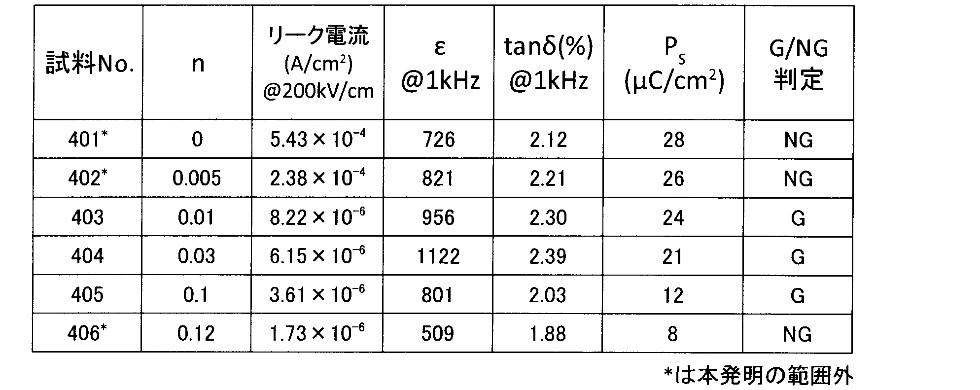
試料No.401(n=0.00、BaHfO3が含まれていないもの)および試料No.402(n=0.005)は、リーク電流が5.43×10⁻⁵A/cm2以上であるため、不良品(NG)と判定された。試料No.406(n=0.12)は、自発分極Psが10μC/cm2未満であるため、不良品(NG)と判定された。一方、試料No.403(n=0.01)、試料No.404(n=0.03)、および、試料No.405(n=0.10)は、リーク電流が5.43×10-5A/cm2以下であり、かつ自発分極Psが10μC/cm2以上であるため、良品(G)と判定された。
すなわち、試料No.402は、リーク電流が2.38×10⁻⁴A/cm2であり、試料No.401(BaHfO3が含まれていないもの)のリーク電流である5.43×10-4A/cm2とほとんど変わらなかった。しかし、試料No.403、試料No.404、試料No.405、試料No.406は、それぞれ、リーク電流が8.22×10-6A/cm2、6.15×10-6A/cm2、3.61×10-6A/cm2、1.73×10-6A/cm2であり、良好なリーク電流特性が得られた。
さらに、試料No.401~試料No.406は、それぞれ、自発分極Psが28μC/cm2、26μC/cm2、24μC/cm2、21μC/cm2、12μC/cm2、8μC/cm2であり、nが大きくなる(言い換えると,BaHfO3の割合が多くなる)につれて、自発分極Psが減少する傾向が見られた。そして、試料No.406(n=0.12)は、自発分極Psが10μC/cm2未満であり、非常に小さくなった。
以上のことから、(K0.45Na0.55)Nb0.95O3に対して、BaHfO3が0.01≦n≦0.10の範囲で固溶されたニオブ酸カリウムナトリウム系薄膜16は、優れた強誘電体特性を維持した状態で、リーク電流特性を改善できることが判る。
さらに、試料No.401~試料No.406の圧電定数d33
*が前記第1の実施の形態と同様にして求められた。測定結果は表20に示されている。

試料No.402~試料No.405の圧電定数d33
*は、それぞれ、120.6pm/V、123.7pm/V、128.7pm/V、111.9pm/Vであり、試料No.401(BaHfO3が含まれていないもの)の124.0pm/Vと同等の値であった。一方、試料No.406(n=0.12)の圧電定数d33
*は、89.2pm/Vと、急激に小さくなった。これは、自発分極Psの値が10μC/cm2以下と、非常に小さくなっているためである。
本第5の実施の形態は、100モルの(K0.45Na0.55)Nb0.95O3に対して、2モルのMnを含有した試料について評価した。しかし、100モルの主成分(1-n)(K0.45Na0.55)Nb0.95O3-nBaHfO3に対して、10モル以下のMnを含有した試料についても、本第5の実施の形態と同様の評価結果が得られた。
(第6の実施の形態の圧電体薄膜素子の製造)
第6の実施の形態の圧電体薄膜素子は、図2に示した前記第1の実施の形態の圧電体薄膜素子と同様の構成を有している。
第6の実施の形態の圧電体薄膜素子は、図2に示した前記第1の実施の形態の圧電体薄膜素子と同様の構成を有している。
なお、第6の実施の形態では、圧電体薄膜16である一般式(1-n)(K1-xNax)NbyO3-nBaHfO3で表示されるニオブ酸カリウムナトリウム系薄膜におけるxおよびyが変化している。
圧電体薄膜16、すなわち、ニオブ酸カリウムナトリウム(KNN)系薄膜16は、化学溶液堆積法を用いて作成される。
まず、原料であるカリウムエトキシド、ナトリウムエトキシド、ペンタエトキシニオブ、マンガンアセチルアセトナト、バリウムエトキシド、および、テトライソプロポキシハフニウムが、モル比で(1.07-x)×0.97:(x+0.17)×0.97:y×0.97:0.02×0.97:0.03:0.03となるように準備される。ここで、本第6の実施の形態の場合、x、yは、条件式0.2≦x≦1.00、および、条件式0.85≦y≦1.10を満足する。
まず、原料であるカリウムエトキシド、ナトリウムエトキシド、ペンタエトキシニオブ、マンガンアセチルアセトナト、バリウムエトキシド、および、テトライソプロポキシハフニウムが、モル比で(1.07-x)×0.97:(x+0.17)×0.97:y×0.97:0.02×0.97:0.03:0.03となるように準備される。ここで、本第6の実施の形態の場合、x、yは、条件式0.2≦x≦1.00、および、条件式0.85≦y≦1.10を満足する。
その後、第5の実施の形態と同様の方法で、基板12、基板12上に形成された下部電極14、下部電極14上に形成された圧電体薄膜16、および、圧電体薄膜16上に形成された上部電極18にて構成されている圧電体薄膜素子が作成される。
圧電体薄膜16は、膜厚が300nmで、組成が0.97(K1-xNax)NbyO3-0.03BaHfO3(0.2≦x≦1.00、0.85≦y≦1.10)のニオブ酸カリウムナトリウム(KNN)系薄膜である。
(第6の実施の形態の圧電体薄膜素子の評価)
表21、表22および表23は、0.97(K1-xNax)NbyO3-0.03BaHfO3におけるx及びyを、0.2≦x≦1.00、0.85≦y≦1.10の範囲で変化させたときの、200kV/cmの電界におけるリーク電流、1kHzの周波数における誘電率ε及びtanδ、測定周波数10kHzで印加電界500kV/cmで測定した際の自発分極Psの値を示す(試料No.404、試料No.407~試料No.507)。なお、前記第5の実施の形態と同様に、リーク電流が5.43×10-5A/cm2以下で、かつ、自発分極Psが10μC/cm2以上の場合は、良品(G)と判定し、それ以外の場合は不良品(NG)と判定した。
表21、表22および表23は、0.97(K1-xNax)NbyO3-0.03BaHfO3におけるx及びyを、0.2≦x≦1.00、0.85≦y≦1.10の範囲で変化させたときの、200kV/cmの電界におけるリーク電流、1kHzの周波数における誘電率ε及びtanδ、測定周波数10kHzで印加電界500kV/cmで測定した際の自発分極Psの値を示す(試料No.404、試料No.407~試料No.507)。なお、前記第5の実施の形態と同様に、リーク電流が5.43×10-5A/cm2以下で、かつ、自発分極Psが10μC/cm2以上の場合は、良品(G)と判定し、それ以外の場合は不良品(NG)と判定した。
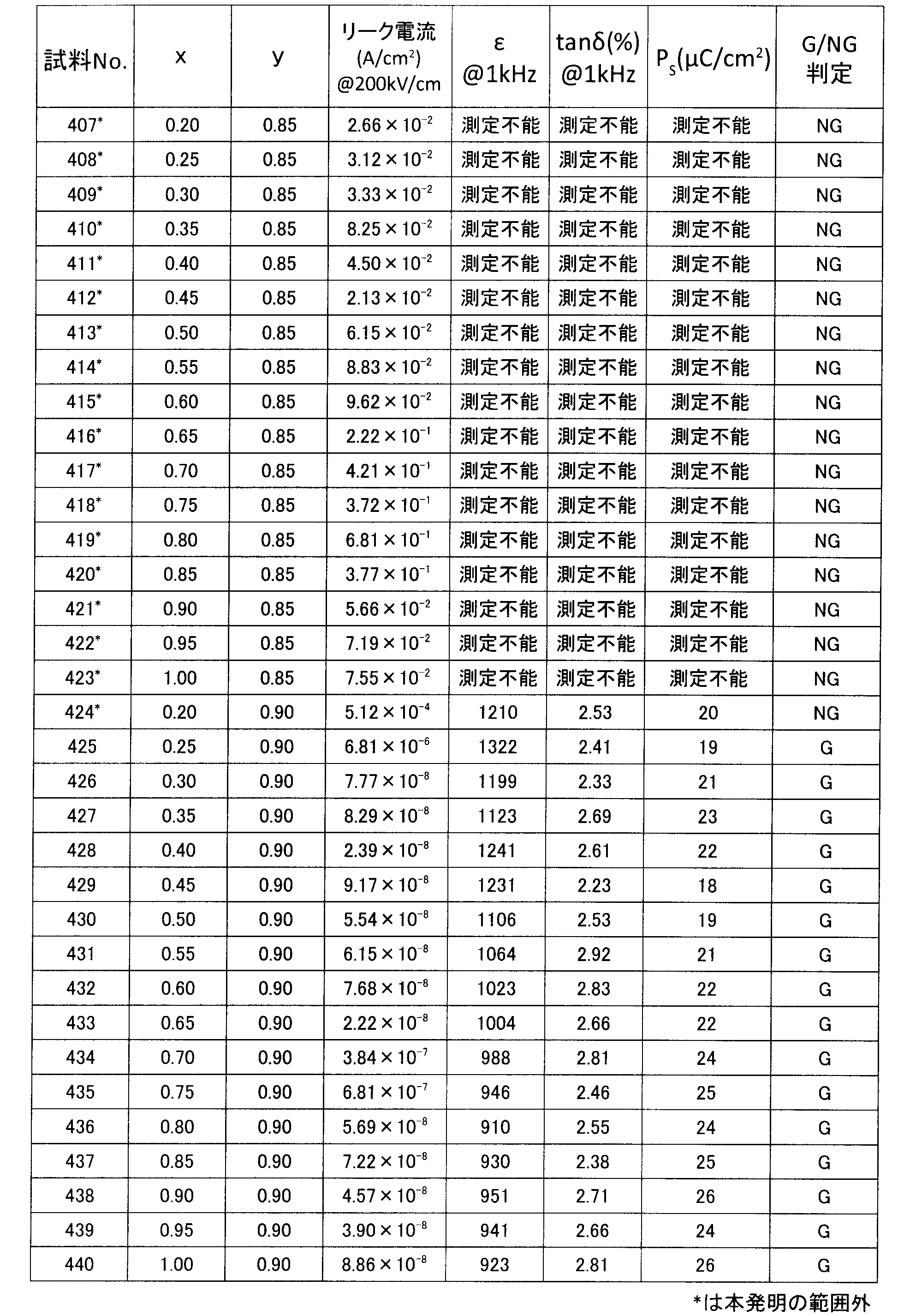
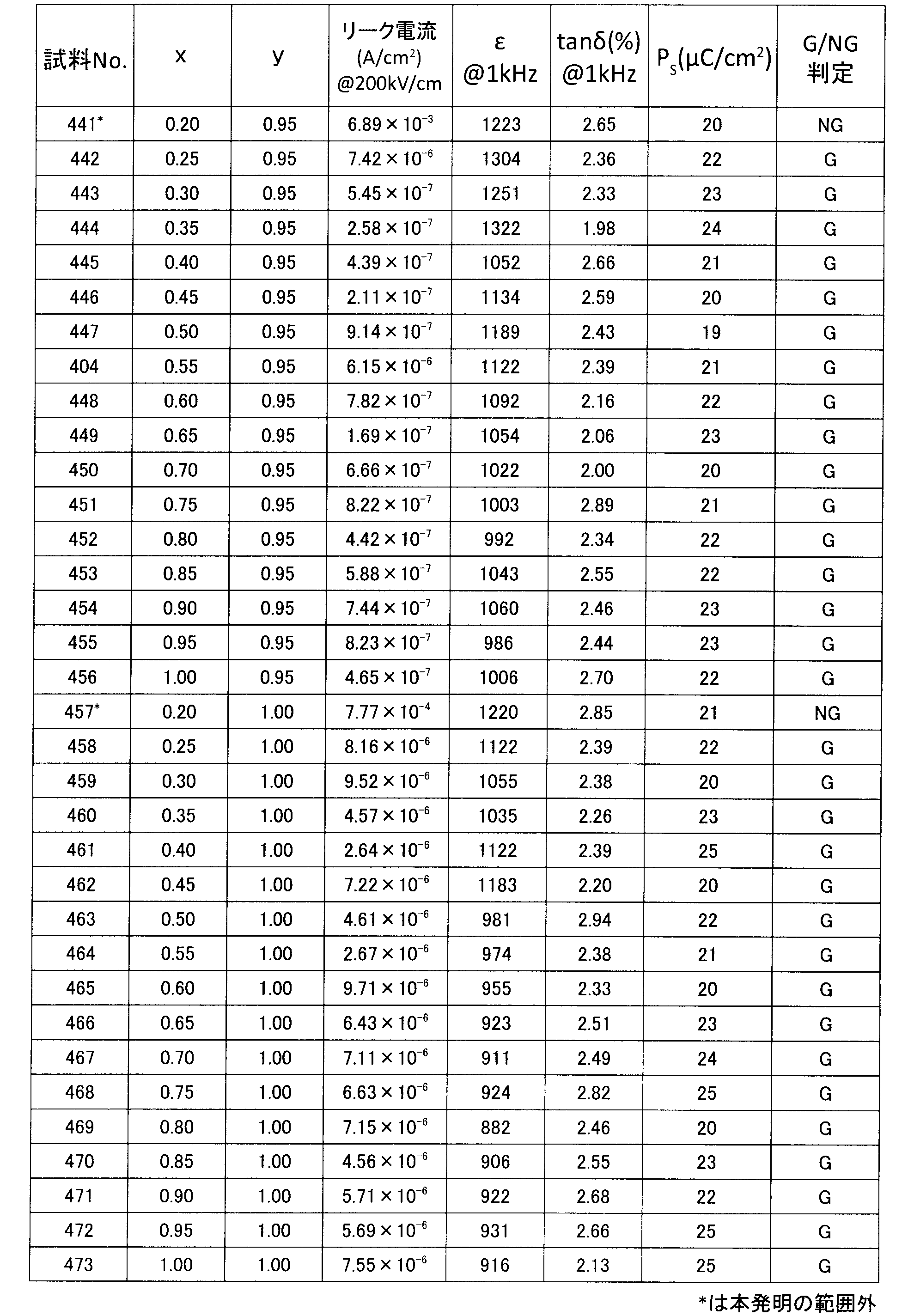

表21の試料No.407~試料No.423は、y=0.85で、xを0.20≦x≦1.00の範囲で変化させたときの試料である。これらの試料は、リーク電流が2.13×10⁻²A/cm2~6.81×10-1A/cm2と高く、BaHfO3を固溶させた効果が見られない。従って、試料No.407~試料No.423は、不良品(NG)と判定された。これは、Aサイトの(K1-x,Nax,Ba)とBサイトの(Nby,Hf)のモル比が、化学量論的な組成から大きく外れているためである。
試料No.424~試料No.440は、y=0.90で、xを0.20≦x≦1.00の範囲で変化させたときの試料である。その中で、x=0.20の試料(試料No.424)は、リーク電流が5.12×10⁻⁴A/cm2である。この値は、BaHfO3が含まれていない試料No.401と比較して、殆んど変化が見られず、不良品(NG)と判定された。
一方、0.25≦x≦1.00の試料(試料No.425~試料No.440)は、リーク電流が2.22×10⁻⁸A/cm2~6.81×10-6A/cm2である。これらの値は、BaHfO3が含まれていない試料No.401と比較して、大幅なリーク電流の向上が見られた。さらに、自発分極Psは18~26μC/cm2であり、強誘電体特性も維持していた。従って、0.25≦x≦1.00の試料(試料No.425~試料No.440)は、良品(G)と判定された。
表22の試料No.404および試料No.441~試料No.456は、y=0.95で、xを0.20≦x≦1.00の範囲で変化させたときの試料である。その中で、x=0.20の試料(試料No.441)は、リーク電流が6.89×10⁻³A/cm2である。この値は、BaHfO3が含まれていない試料No.401と比較して、悪化しているため、不良品(NG)と判定された。
一方、0.25≦x≦1.00の試料(試料No.404および試料No.442~試料No.456)は、リーク電流が1.69×10⁻⁷A/cm2~7.42×10-6A/cm2である。これらの値は、BaHfO3が含まれていない試料No.401と比較して、大幅なリーク電流の向上が見られた。さらに、自発分極Psは19~24μC/cm2であり、強誘電体特性も維持していた。従って、0.25≦x≦1.00の試料(試料No.404および試料No.442~試料No.456)は、良品(G)と判定された。
試料No.457~試料No.473は、y=1.00で、xを0.20≦x≦1.00の範囲で変化させたときの試料である。その中で、x=0.20の試料(試料No.457)は、リーク電流が7.77×10⁻⁴A/cm2である。この値は、BaHfO3が含まれていない試料No.401と比較して、悪化しているため、不良品(NG)と判定された。
一方、0.25≦x≦1.00の試料(試料No.458~試料No.473)は、リーク電流が2.64×10⁻⁶A/cm2~9.71×10-6A/cm2である。これらの値は、BaHfO3が含まれていない試料No.401と比較して、大幅なリーク電流の向上が見られた。さらに、自発分極Psは20~25μC/cm2であり、強誘電体特性も維持していた。従って、0.25≦x≦1.00の試料(試料No.458~試料No.473)は、良品(G)と判定された。
表23の試料No.474~試料No.490は、y=1.05で、xを0.20≦x≦1.00の範囲で変化させたときの試料である。その中で、x=0.20の試料(試料No.474)は、リーク電流が4.12×10⁻⁴A/cm2である。この値は、BaHfO3が含まれていない試料No.401と比較して、悪化しているため、不良品(NG)と判定された。
一方、0.25≦x≦1.00の試料(試料No.475~試料No.490)は、リーク電流が1.26×10⁻⁶A/cm2~8.22×10-6A/cm2である。これらの値は、BaHfO3が含まれていない試料No.401と比較して、大幅なリーク電流の向上が見られた。さらに、自発分極Psは20~24μC/cm2と強誘電体特性も維持していた。従って、0.25≦x≦1.00の試料(試料No.475~試料No.490)は、良品(G)と判定された。
試料No.491~試料No.507は、y=1.10で、xを0.20≦x≦1.00の範囲で変化させたときの試料である。これらの試料は、リーク電流が1.53×10⁻³A/cm2~8.99×10-3A/cm2と高く、BaHfO3を固溶させた効果が見られない。従って、試料No.491~試料No.507は、不良品(NG)と判定された。これは、Aサイトの(K1-x,Nax,Ba)とBサイトの(Nby,Hf)のモル比が、化学量論的な組成から大きく外れているためである。
また、良品(G)と判定された試料は、全てtanδが3%以下であり、非常に低い。従って、高品質なニオブ酸カリウムナトリウム系薄膜16が作成されていることが判る。
さらに、上記の良品/不良品(G/NG)判定で、良品(G)と判定された試料(試料No.404、試料No.425~試料No.440など)の圧電定数d33
*が、前記第2の実施の形態と同様にして求められた。測定結果は表24および表25に示されている。

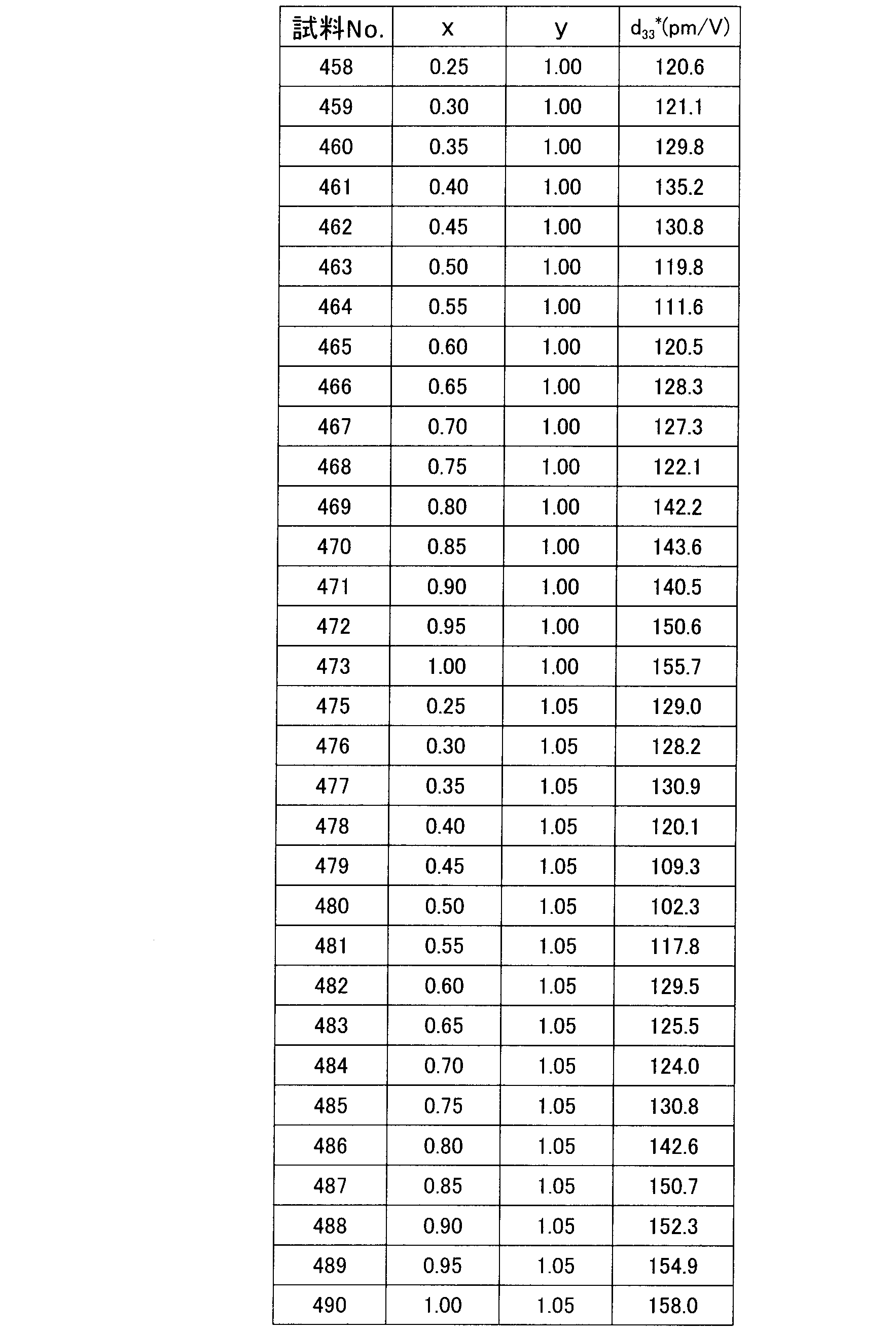
表24および表25より、圧電定数d33
*は、102.3~158.6pm/Vであり、試料No.401(BaHfrO3が含まれていないもの)の124.0pm/Vと殆んど変わらないことが判る。これは、自発分極Psの値が10μC/cm2以上と、大きな値を示しているためである。
特に、xの範囲が0.80≦x≦1.00の試料(試料No.436~試料No.440など)は、圧電定数d33
*が140.3~158.6pm/Vであり、試料No.401(BaHfO3が含まれていないもの)の124.0pm/Vと比較して、非常に大きな数値であることが判る。
表26は、x=0.90、y=0.95、n=0.03としたときの、0.97(K0.1Na0.9)Nb0.95O3-0.03M1HfO3(M1=Ca,Sr)において、200kV/cmの電界におけるリーク電流、1kHzの周波数における誘電率ε及びtanδ、測定周波数10kHzで印加電界500kV/cmで測定した際の自発分極Ps及び圧電定数d33
*の値を示す(試料No.508,509)。

表26より、M1=Caの試料(試料No.508)は、リーク電流が2.13×10⁻⁶A/cm2であり、低かった。さらに、自発分極Psは22μC/cm2であり、強誘電性も維持していた。従って、M1=Caの試料(試料No.508)は、良品(G)と判定された。
また、M1=Srの試料(試料No.509)についても、リーク電流が5.96×10⁻⁶A/cm2であり、低かった。さらに、自発分極Psは22μC/cm2であり、強誘電性も維持していた。従って、M1=Srの試料(試料No.509)は、良品(G)と判定された。
なお、これらのM1=Ca,Srの試料(試料No.508,509)の圧電定数d33
*は、それぞれ、153.4pm/V及び150.4pm/Vであり、M1HfO3(M1=Ca,Sr)が含まれていない試料と比較して、圧電定数d33
*の向上が見られた。
本第6の実施の形態は、100モルの(K1-xNax)NbyO3に対して、2モルのMnを含有した試料について評価した。しかし、100モルの主成分0.97(K1-xNax)NbyO3-0.03M1HfO3(M1=Ca,Sr,Ba)に対して、10モル以下のMnを含有した試料についても、本第6の実施の形態と同様の評価結果が得られた。
従って、本第6の実施の形態における評価結果から、圧電体薄膜16である一般式(1-n)(K1-xNax)NbyO3-nM1HfO3(M1=Ca,Sr,Ba)で表示されるニオブ酸カリウムナトリウム系薄膜において、0.25≦x≦1.00、0.90≦y≦1.05とすることで、リーク電流特性、強誘電体特性及び圧電体特性に優れた圧電体薄膜素子を得られることが明らかとなった。
図5は、試料No.404の強誘電体ヒステリシス曲線を示す。ニオブ酸カリウムナトリウムにBaHfO3を固溶させることによって、100kV/cm以上の電界におけるリーク電流特性が向上し、最大印加電圧1MV/cm、測定周波数100Hzにおいても良好な強誘電体ヒステリシス曲線を示すことが判る。
このように本発明に係る圧電体薄膜素子において、圧電体薄膜の一般式(1-n)(K1-xNax)NbyO3-nM1HfO3(M1=Ca,Sr,Ba)で表示されるニオブ酸カリウムナトリウム系薄膜であって、x、yおよびnの範囲が、それぞれ、0.25≦x≦1.00、0.90≦y≦1.05および0.01≦n≦0.10とすることにより、リーク電流特性、強誘電体特性および圧電体特性に優れた圧電体薄膜素子が得られる。さらに、強誘電体薄膜素子や圧電体薄膜素子の使用の際に問題になる静電容量の温度変化が、抑えられる。
なお、この発明は、前記実施の形態に限定されるものではなく、その要旨の範囲内で種々に変形される。ニオブ酸カリウムナトリウム系薄膜16は、化学溶液堆積法によって作成されているけれども、作成したニオブ酸カリウムナトリウム系薄膜16の組成が本発明の範囲にあれば、例えば、スパッタリング法、化学気相成長法、エアロゾル堆積法、パルスレーザー堆積法などで作成してもよい。
Claims (6)
- 電極と圧電体薄膜とを備えた圧電体薄膜素子であって、
前記圧電体薄膜が、一般式(1-n)(K1-xNax)NbyO3-nBaZrO3を主成分とするニオブ酸カリウムナトリウム系薄膜であって、前記x、yおよびnが、それぞれ、0.25≦x≦0.75、0.85≦y≦1.10、0.01≦n≦0.10の範囲であること、を特徴とする、圧電体薄膜素子。 - 電極と圧電体薄膜とを備えた圧電体薄膜素子であって、
前記圧電体薄膜が、一般式(1-n)(K1-xNax)NbyO3-nBaSnO3を主成分とするニオブ酸カリウムナトリウム系薄膜であって、前記x、yおよびnが、それぞれ、0.25≦x≦0.75、0.90≦y≦1.05、0.01≦n≦0.10の範囲であること、を特徴とする、圧電体薄膜素子。 - 電極と圧電体薄膜とを備えた圧電体薄膜素子であって、
前記圧電体薄膜が、一般式(1-n)(K1-xNax)NbyO3-nM1M2O3で表されると共に、M1がCa、SrおよびBaのいずれか一つであり、M2がZrであるものを主成分とするニオブ酸カリウムナトリウム系薄膜であって、前記x、yおよびnが、それぞれ、0.25≦x≦1.00、0.85≦y≦1.10、0.01≦n≦0.10の範囲であること、を特徴とする、圧電体薄膜素子。 - 電極と圧電体薄膜とを備えた圧電体薄膜素子であって、
前記圧電体薄膜が、一般式(1-n)(K1-xNax)NbyO3-nM1M2O3で表されると共に、M1がCa、SrおよびBaのいずれか一つであり、M2がSnおよびHfのいずれか一つであるものを主成分とするニオブ酸カリウムナトリウム系薄膜であって、前記x、yおよびnが、それぞれ、0.25≦x≦1.00、0.90≦y≦1.05、0.01≦n≦0.10の範囲であること、を特徴とする、圧電体薄膜素子。 - 前記x、yおよびnが、それぞれ、0.80≦x≦1.00、0.85≦y≦1.10、0.01≦n≦0.10の範囲であること、を特徴とする、請求項3に記載の圧電体薄膜素子。
- 前記x、yおよびnが、それぞれ、0.80≦x≦1.00、0.90≦y≦1.05、0.01≦n≦0.10の範囲であること、を特徴とする、請求項4に記載の圧電体薄膜素子。
Priority Applications (2)
| Application Number | Priority Date | Filing Date | Title |
|---|---|---|---|
| JP2013509883A JP5418725B2 (ja) | 2011-04-15 | 2012-04-06 | 圧電体薄膜素子 |
| US14/053,902 US9437805B2 (en) | 2011-04-15 | 2013-10-15 | Piezoelectric thin film element |
Applications Claiming Priority (4)
| Application Number | Priority Date | Filing Date | Title |
|---|---|---|---|
| JP2011-090566 | 2011-04-15 | ||
| JP2011090566 | 2011-04-15 | ||
| JP2011264342 | 2011-12-02 | ||
| JP2011-264342 | 2011-12-02 |
Related Child Applications (1)
| Application Number | Title | Priority Date | Filing Date |
|---|---|---|---|
| US14/053,902 Continuation US9437805B2 (en) | 2011-04-15 | 2013-10-15 | Piezoelectric thin film element |
Publications (1)
| Publication Number | Publication Date |
|---|---|
| WO2012141105A1 true WO2012141105A1 (ja) | 2012-10-18 |
Family
ID=47009278
Family Applications (1)
| Application Number | Title | Priority Date | Filing Date |
|---|---|---|---|
| PCT/JP2012/059561 Ceased WO2012141105A1 (ja) | 2011-04-15 | 2012-04-06 | 圧電体薄膜素子 |
Country Status (3)
| Country | Link |
|---|---|
| US (1) | US9437805B2 (ja) |
| JP (1) | JP5418725B2 (ja) |
| WO (1) | WO2012141105A1 (ja) |
Cited By (6)
| Publication number | Priority date | Publication date | Assignee | Title |
|---|---|---|---|---|
| JP2012253109A (ja) * | 2011-06-01 | 2012-12-20 | Hitachi Cable Ltd | 圧電膜素子及び圧電膜デバイス |
| WO2014084265A1 (ja) * | 2012-11-27 | 2014-06-05 | 富山県 | 圧電セラミックスの製造方法、圧電セラミックス、および圧電素子 |
| JP2014107563A (ja) * | 2012-11-28 | 2014-06-09 | Tdk Corp | 圧電素子、圧電アクチュエータ、及び圧電センサ、並びにハードディスクドライブ、及びインクジェットプリンタ装置 |
| WO2014119705A1 (en) * | 2013-01-29 | 2014-08-07 | Canon Kabushiki Kaisha | Piezoelectric material, piezoelectric element, and electronic equipment |
| US10297742B2 (en) * | 2016-11-16 | 2019-05-21 | Seiko Epson Corporation | Piezoelectric element and device including the same |
| KR20250011282A (ko) * | 2023-07-14 | 2025-01-21 | 경상국립대학교산학협력단 | 데이터 센터 화재 방지용 냉각 소자 제조방법 및 이를 이용한 데이터 센터 화재 방지 장치 |
Families Citing this family (8)
| Publication number | Priority date | Publication date | Assignee | Title |
|---|---|---|---|---|
| US9277869B2 (en) * | 2012-11-28 | 2016-03-08 | Tdk Corporation | Thin-film piezoelectric element, thin-film piezoelectric actuator, thin-film piezoelectric sensor, hard disk drive, and inkjet printer apparatus |
| US9331262B2 (en) * | 2013-05-20 | 2016-05-03 | Tdk Corporation | Thin film piezoelectric element, thin film piezoelectric actuator, thin film piezoelectric sensor, hard drive disk, and inkjet printer device |
| JP6578866B2 (ja) * | 2015-10-02 | 2019-09-25 | Tdk株式会社 | 圧電薄膜、圧電薄膜素子、圧電アクチュエータ、圧電センサ、並びにハードディスクドライブ、及びインクジェットプリンタヘッド |
| JP6874351B2 (ja) * | 2016-12-07 | 2021-05-19 | Tdk株式会社 | 圧電薄膜積層体、圧電薄膜基板、圧電薄膜素子、圧電アクチュエータ、圧電センサ、ヘッドアセンブリ、ヘッドスタックアセンブリ、ハードディスクドライブ、プリンタヘッド、及びインクジェットプリンタ装置 |
| JP6790776B2 (ja) * | 2016-12-07 | 2020-11-25 | Tdk株式会社 | 圧電薄膜積層体、圧電薄膜基板、圧電薄膜素子、圧電アクチュエータ、圧電センサ、ヘッドアセンブリ、ヘッドスタックアセンブリ、ハードディスクドライブ、プリンタヘッド、及びインクジェットプリンタ装置 |
| JP6958045B2 (ja) * | 2017-07-11 | 2021-11-02 | セイコーエプソン株式会社 | 圧電素子およびその製造方法、ならびに圧電素子応用デバイス |
| EP3767285B1 (en) * | 2018-07-04 | 2025-01-08 | Murata Manufacturing Co., Ltd. | Compound sensor |
| JP7362339B2 (ja) * | 2019-08-02 | 2023-10-17 | 住友化学株式会社 | 圧電積層体、圧電素子、および圧電積層体の製造方法 |
Citations (4)
| Publication number | Priority date | Publication date | Assignee | Title |
|---|---|---|---|---|
| JPH10270771A (ja) * | 1997-03-26 | 1998-10-09 | Konica Corp | 圧電素子の製造方法及びそれにより製造された圧電素子 |
| WO2005021461A1 (ja) * | 2003-08-28 | 2005-03-10 | National Institute Of Advanced Industrial Science And Technology | ペロブスカイト固溶体組成物およびこのものから得られる圧電セラミックス |
| JP2009049065A (ja) * | 2007-08-14 | 2009-03-05 | Hitachi Cable Ltd | 圧電薄膜素子 |
| JP2009242166A (ja) * | 2008-03-31 | 2009-10-22 | Tdk Corp | 圧電磁器及びその製造方法、並びに当該圧電磁器を用いた圧電素子 |
Family Cites Families (14)
| Publication number | Priority date | Publication date | Assignee | Title |
|---|---|---|---|---|
| JP5360519B2 (ja) * | 2006-09-22 | 2013-12-04 | 西川 正名 | 電気浸透材及びその製造方法と電気浸透流ポンプ |
| JP2008159807A (ja) | 2006-12-22 | 2008-07-10 | Hitachi Cable Ltd | 圧電薄膜素子及び圧電薄膜素子を用いて製造したアクチュエータとセンサ |
| DE102008042955A1 (de) * | 2007-11-08 | 2009-05-14 | Denso Corp., Kariya-shi | Verfahren zum Herstellen einer Keramik mit Kristallorientierung |
| JP5525143B2 (ja) * | 2008-06-05 | 2014-06-18 | 日立金属株式会社 | 圧電薄膜素子及び圧電薄膜デバイス |
| JP5515675B2 (ja) * | 2009-11-20 | 2014-06-11 | 日立金属株式会社 | 圧電薄膜素子及び圧電薄膜デバイス |
| JP5056914B2 (ja) * | 2010-07-07 | 2012-10-24 | 日立電線株式会社 | 圧電薄膜素子および圧電薄膜デバイス |
| TWI545814B (zh) * | 2012-11-02 | 2016-08-11 | 佳能股份有限公司 | 壓電式材料、壓電式元件及電子設備 |
| WO2014069493A1 (en) * | 2012-11-02 | 2014-05-08 | Canon Kabushiki Kaisha | Piezoelectric material, piezoelectric element, and electronic equipment |
| EP2980040B1 (en) * | 2013-03-29 | 2016-11-30 | NGK Spark Plug Co., Ltd. | Unleaded piezoelectric ceramic composition, piezoelectric element using same, device, and method for manufacturing unleaded piezoelectric ceramic composition |
| US20140339458A1 (en) * | 2013-05-14 | 2014-11-20 | Tdk Corporation | Piezoelectric ceramic and piezoelectric device containing the same |
| US9331262B2 (en) * | 2013-05-20 | 2016-05-03 | Tdk Corporation | Thin film piezoelectric element, thin film piezoelectric actuator, thin film piezoelectric sensor, hard drive disk, and inkjet printer device |
| JP2015135958A (ja) * | 2013-12-18 | 2015-07-27 | キヤノン株式会社 | 圧電材料、圧電素子、および電子機器 |
| EP2953177B1 (en) * | 2014-05-30 | 2017-01-25 | Canon Kabushiki Kaisha | Piezoelectric material, piezoelectric element, and electronic device |
| CN105536514A (zh) * | 2014-10-31 | 2016-05-04 | 通用电气公司 | 用于去除氮氧化物的电极组成、装置和方法 |
-
2012
- 2012-04-06 JP JP2013509883A patent/JP5418725B2/ja active Active
- 2012-04-06 WO PCT/JP2012/059561 patent/WO2012141105A1/ja not_active Ceased
-
2013
- 2013-10-15 US US14/053,902 patent/US9437805B2/en active Active
Patent Citations (4)
| Publication number | Priority date | Publication date | Assignee | Title |
|---|---|---|---|---|
| JPH10270771A (ja) * | 1997-03-26 | 1998-10-09 | Konica Corp | 圧電素子の製造方法及びそれにより製造された圧電素子 |
| WO2005021461A1 (ja) * | 2003-08-28 | 2005-03-10 | National Institute Of Advanced Industrial Science And Technology | ペロブスカイト固溶体組成物およびこのものから得られる圧電セラミックス |
| JP2009049065A (ja) * | 2007-08-14 | 2009-03-05 | Hitachi Cable Ltd | 圧電薄膜素子 |
| JP2009242166A (ja) * | 2008-03-31 | 2009-10-22 | Tdk Corp | 圧電磁器及びその製造方法、並びに当該圧電磁器を用いた圧電素子 |
Cited By (11)
| Publication number | Priority date | Publication date | Assignee | Title |
|---|---|---|---|---|
| JP2012253109A (ja) * | 2011-06-01 | 2012-12-20 | Hitachi Cable Ltd | 圧電膜素子及び圧電膜デバイス |
| WO2014084265A1 (ja) * | 2012-11-27 | 2014-06-05 | 富山県 | 圧電セラミックスの製造方法、圧電セラミックス、および圧電素子 |
| JPWO2014084265A1 (ja) * | 2012-11-27 | 2017-01-05 | 富山県 | 圧電セラミックスの製造方法、圧電セラミックス、および圧電素子 |
| JP2014107563A (ja) * | 2012-11-28 | 2014-06-09 | Tdk Corp | 圧電素子、圧電アクチュエータ、及び圧電センサ、並びにハードディスクドライブ、及びインクジェットプリンタ装置 |
| WO2014119705A1 (en) * | 2013-01-29 | 2014-08-07 | Canon Kabushiki Kaisha | Piezoelectric material, piezoelectric element, and electronic equipment |
| JP2014168054A (ja) * | 2013-01-29 | 2014-09-11 | Canon Inc | 圧電材料、圧電素子、および電子機器 |
| US20150368161A1 (en) * | 2013-01-29 | 2015-12-24 | Canon Kabushiki Kaisha | Piezoelectric material, piezoelectric element, and electronic equipment |
| US10308557B2 (en) | 2013-01-29 | 2019-06-04 | Canon Kabushiki Kaisha | Piezoelectric material, piezoelectric element, and electronic equipment |
| US10297742B2 (en) * | 2016-11-16 | 2019-05-21 | Seiko Epson Corporation | Piezoelectric element and device including the same |
| KR20250011282A (ko) * | 2023-07-14 | 2025-01-21 | 경상국립대학교산학협력단 | 데이터 센터 화재 방지용 냉각 소자 제조방법 및 이를 이용한 데이터 센터 화재 방지 장치 |
| KR102904884B1 (ko) * | 2023-07-14 | 2025-12-26 | 경상국립대학교산학협력단 | 데이터 센터 화재 방지용 냉각 소자 제조방법 및 이를 이용한 데이터 센터 화재 방지 장치 |
Also Published As
| Publication number | Publication date |
|---|---|
| JPWO2012141105A1 (ja) | 2014-07-28 |
| JP5418725B2 (ja) | 2014-02-19 |
| US20140049138A1 (en) | 2014-02-20 |
| US9437805B2 (en) | 2016-09-06 |
Similar Documents
| Publication | Publication Date | Title |
|---|---|---|
| JP5418725B2 (ja) | 圧電体薄膜素子 | |
| Samanta et al. | Band gap, piezoelectricity and temperature dependence of differential permittivity and energy storage density of PZT with different Zr/Ti ratios | |
| Zhao et al. | Large strain of temperature insensitive in (1–x)(0.94 Bi0. 5Na0. 5TiO3–0.06 BaTiO3)–xSr0. 7La0. 2TiO3 lead-free ceramics | |
| JP6296207B2 (ja) | 誘電体薄膜、容量素子および電子部品 | |
| Pečnik et al. | Combined effects of thickness, grain size and residual stress on the dielectric properties of Ba0. 5Sr0. 5TiO3 thin films | |
| Muhsen et al. | The effects of Ca, Zr and Sn substitutions into a ternary system of BaTiO3–BaSnO3–BaZrO3 towards its dielectric and piezoelectric properties: a review | |
| Jaita et al. | Lead‐Free (Ba0. 70Sr0. 30) TiO3‐Modified Bi0. 5 (Na0. 80K0. 20) 0.5 TiO3 Ceramics with Large Electric Field–Induced Strains | |
| Zhang et al. | Sol‐gel processed highly (100)‐textured (K, Na) NbO3‐based lead‐free thin films: Effect of pyrolysis temperature | |
| Xie et al. | Energy storage properties of low concentration Fe-doped barium strontium titanate thin films | |
| Tkach et al. | Mechanical strain engineering of dielectric tunability in polycrystalline SrTiO 3 thin films | |
| Jiang et al. | Effects of Mn-doping on the properties of (Ba0. 92Ca0. 08)(Ti0. 95Zr0. 05) O3 lead-free ceramics | |
| Kang et al. | Dielectric properties of Pb (In1/2Nb1/2) O3–Pb (Mg1/3Nb2/3) O3–PbTiO3 film by aerosol deposition for energy storage applications | |
| WO2015060004A1 (ja) | 非鉛誘電体薄膜及びこの薄膜形成用組成物並びにこの薄膜の形成方法 | |
| Li et al. | Energy storage property of (Pb0. 97La0. 02)(Zr0. 5Sn0. 4Ti0. 1) O3-(Na0. 5Bi0. 5) 0.94 Ba0. 06TiO3 ceramics: Effects of antiferroelectric-relaxor transition and improved breakdown strength | |
| WO2015060003A1 (ja) | 非鉛誘電体薄膜形成用液組成物及びその薄膜の形成方法並びにその方法で形成された非鉛誘電体薄膜 | |
| Xu et al. | Structure and dielectric properties of (Na0. 5Bi0. 5) TiO3–SrTiO3 thick films derived from polyvinylpyrrolidone-modified chemical solution | |
| WO2012141104A1 (ja) | 強誘電体薄膜およびその製造方法 | |
| Yao et al. | Effects of Nb and Mg doping on the dielectric and electromechanical properties of PbZrO3 thin films | |
| Samantaray et al. | Effect of post-deposition annealing on microstructural and optical properties of barium strontium titanate thin films deposited by rf magnetron sputtering | |
| Sultana et al. | Frequency-driven dielectric analysis of ultrathin HfOx-TiOx composite films | |
| Cho et al. | Ferroelectric relaxor properties of (1− x) K0. 5Na0. 5NbO3–xBa0. 5Ca0. 5TiO3 ceramics | |
| Yu et al. | Ba0. 6Sr0. 4TiO3–Bi1. 5Mg1. 0Nb1. 5O7 composite thin film capacitors with enhanced tunable performance for tunable device applications | |
| Chen et al. | Microstructures and electrical properties of lead-based PBZNZT and lead-free BNKT piezoelectric ceramics using microwave sintering | |
| TWI895323B (zh) | 強介電性薄膜、使用其之電子元件及強介電性薄膜之製造方法 | |
| Chiu et al. | Effect of MgO dopant on the microstructure and dielectric properties of rf-sputtered Ba0. 5Sr0. 5TiO3 thin films |
Legal Events
| Date | Code | Title | Description |
|---|---|---|---|
| 121 | Ep: the epo has been informed by wipo that ep was designated in this application |
Ref document number: 12771404 Country of ref document: EP Kind code of ref document: A1 |
|
| ENP | Entry into the national phase |
Ref document number: 2013509883 Country of ref document: JP Kind code of ref document: A |
|
| NENP | Non-entry into the national phase |
Ref country code: DE |
|
| 122 | Ep: pct application non-entry in european phase |
Ref document number: 12771404 Country of ref document: EP Kind code of ref document: A1 |