WO2012140949A1 - コネクタ - Google Patents
コネクタ Download PDFInfo
- Publication number
- WO2012140949A1 WO2012140949A1 PCT/JP2012/053427 JP2012053427W WO2012140949A1 WO 2012140949 A1 WO2012140949 A1 WO 2012140949A1 JP 2012053427 W JP2012053427 W JP 2012053427W WO 2012140949 A1 WO2012140949 A1 WO 2012140949A1
- Authority
- WO
- WIPO (PCT)
- Prior art keywords
- magnetic
- connector
- conductor
- sheet
- magnetic sheet
- Prior art date
- Legal status (The legal status is an assumption and is not a legal conclusion. Google has not performed a legal analysis and makes no representation as to the accuracy of the status listed.)
- Ceased
Links
Images






Classifications
-
- H—ELECTRICITY
- H05—ELECTRIC TECHNIQUES NOT OTHERWISE PROVIDED FOR
- H05K—PRINTED CIRCUITS; CASINGS OR CONSTRUCTIONAL DETAILS OF ELECTRIC APPARATUS; MANUFACTURE OF ASSEMBLAGES OF ELECTRICAL COMPONENTS
- H05K9/00—Screening of apparatus or components against electric or magnetic fields
- H05K9/0073—Shielding materials
- H05K9/0075—Magnetic shielding materials
-
- H—ELECTRICITY
- H01—ELECTRIC ELEMENTS
- H01R—ELECTRICALLY-CONDUCTIVE CONNECTIONS; STRUCTURAL ASSOCIATIONS OF A PLURALITY OF MUTUALLY-INSULATED ELECTRICAL CONNECTING ELEMENTS; COUPLING DEVICES; CURRENT COLLECTORS
- H01R13/00—Details of coupling devices of the kinds covered by groups H01R12/70 or H01R24/00 - H01R33/00
- H01R13/648—Protective earth or shield arrangements on coupling devices, e.g. anti-static shielding
- H01R13/658—High frequency shielding arrangements, e.g. against EMI [Electro-Magnetic Interference] or EMP [Electro-Magnetic Pulse]
- H01R13/6598—Shield material
- H01R13/6599—Dielectric material made conductive, e.g. plastic material coated with metal
-
- H—ELECTRICITY
- H01—ELECTRIC ELEMENTS
- H01R—ELECTRICALLY-CONDUCTIVE CONNECTIONS; STRUCTURAL ASSOCIATIONS OF A PLURALITY OF MUTUALLY-INSULATED ELECTRICAL CONNECTING ELEMENTS; COUPLING DEVICES; CURRENT COLLECTORS
- H01R12/00—Structural associations of a plurality of mutually-insulated electrical connecting elements, specially adapted for printed circuits, e.g. printed circuit boards [PCB], flat or ribbon cables, or like generally planar structures, e.g. terminal strips, terminal blocks; Coupling devices specially adapted for printed circuits, flat or ribbon cables, or like generally planar structures; Terminals specially adapted for contact with, or insertion into, printed circuits, flat or ribbon cables, or like generally planar structures
- H01R12/70—Coupling devices
- H01R12/71—Coupling devices for rigid printing circuits or like structures
- H01R12/712—Coupling devices for rigid printing circuits or like structures co-operating with the surface of the printed circuit or with a coupling device exclusively provided on the surface of the printed circuit
- H01R12/716—Coupling device provided on the PCB
-
- H—ELECTRICITY
- H05—ELECTRIC TECHNIQUES NOT OTHERWISE PROVIDED FOR
- H05K—PRINTED CIRCUITS; CASINGS OR CONSTRUCTIONAL DETAILS OF ELECTRIC APPARATUS; MANUFACTURE OF ASSEMBLAGES OF ELECTRICAL COMPONENTS
- H05K1/00—Printed circuits
- H05K1/02—Details
- H05K1/14—Structural association of two or more printed circuits
- H05K1/142—Arrangements of planar printed circuit boards in the same plane, e.g. auxiliary printed circuit insert mounted in a main printed circuit
Definitions
- the present invention relates to a connector for connecting various electronic devices or circuit boards, and more particularly to a connector capable of reducing unnecessary electromagnetic waves generated from various electronic devices.
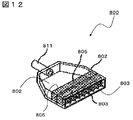
- Patent Document 1 proposes a connector 800 between electronic devices that can absorb leakage of unnecessary electromagnetic waves generated during signal transmission or communication, as shown in FIG. .
- a connector 800 shown in FIG. 12 includes a connector housing 802 provided at the tip of the connection cable 811 and connector pins 803 that are connected to a plurality of transmission lines (not shown) in the connection cable 811. ing. Then, the electromagnetic wave absorbing material 805 is applied to the outside of the connector housing 802 and solidified (conventional example shown in FIG. 12), the electromagnetic wave absorbing material 805 is filled in the connector housing 802, or the synthetic containing the electromagnetic wave absorbing material 805 is contained.
- a connector capable of efficiently absorbing unnecessary electromagnetic waves can be obtained by using a means of molding a resin material into the connector housing 802.
- an electromagnetic wave absorber 805 having an electromagnetic wave absorption characteristic that absorbs electromagnetic field energy by utilizing characteristics such as heat conversion or reflection a soft magnetic magnetic powder processed into a flat shape is used.
- a non-woven cloth type electromagnetic wave absorber “Emicloth” (trade name) manufactured by Mitsubishi Materials Corporation is suitable.
- Patent Document 2 As a type which does not have the connector housing 802 formed in the box shape of the conventional example 1 described above, in Patent Document 2, as shown in FIG. 13, a convex portion 922 in which a part of the base resin plate 920 is projected is provided. A connector 900 for forming a conductor pattern 924 to connect a printed wiring board and a wire harness has been proposed. Since the connector 900 of the conventional example 2 does not have the housing (connector housing 802) found in the conventional example 1, it is difficult to arrange the shield member. Therefore, the connector 900 has no shield measures.
- the present invention solves the above-described problems, and an object thereof is to provide a connector with good EMC performance.
- a connector according to claim 1 of the present invention is provided with a conductor terminal electrically connected to a pin conductor terminal of a mating connector and a conductor pattern electrically connected to the conductor terminal.
- the conductor terminal is formed in a concave depression or a convex protrusion provided in the base, and the depression or the protrusion is a flat magnetic powder.
- the flat magnetic powder is oriented in the in-plane direction of the magnetic sheet and in the longitudinal direction of the conductor terminal. It is characterized by being preferentially oriented toward.
- the connector according to claim 2 of the present invention is characterized in that the conductor terminals are provided on two opposing surfaces of the recess or the protrusion.
- the connector according to claim 3 of the present invention is characterized in that the recess or the protrusion is formed by heating and softening the magnetic sheet to form the recess or the protrusion.
- the connector according to claim 4 of the present invention is characterized in that the forming is vacuum forming in which the magnetic sheet is sucked from the mold side and the magnetic sheet is brought into close contact with the mold.
- the connector according to claim 5 of the present invention is characterized in that the molding is performed by stacking the magnetic sheets.
- the connector according to claim 6 of the present invention is characterized in that the resin of the magnetic sheet is made of a thermoplastic synthetic resin.
- the connector according to claim 7 of the present invention is characterized in that the magnetic loss magnetic loss of the magnetic material sheet is 15 or more in a frequency range of 20 Mhz to 1 Ghz.
- the connector of the present invention is a magnetic body preferentially oriented in the longitudinal direction of the conductor terminal in the concave depression or convex protrusion in which the conductor terminal is formed. Since the sheet has the flat magnetic powder, the direction of the magnetic field of the magnetic sheet can be preferentially aligned in the longitudinal direction of the conductor terminal. Thereby, the electromagnetic wave which comes out of a conductor terminal or enters into a conductor terminal can be shielded with a magnetic material sheet, and a connector with good EMC performance can be provided.
- the connector of the present invention since the connector of the present invention is provided with the conductor terminals on the two opposing faces of the recess or the protrusion having the magnetic sheet containing the flat magnetic powder,
- the magnetic material sheet is arranged along the conductor terminal.
- the electromagnetic wave which comes out of the conductor terminal of both sides, or enters the conductor terminal can be shielded more by the magnetic material sheet
- the connector of the present invention is formed by heating and softening the magnetic sheet to form a recess or a protrusion, the magnetic body that shields electromagnetic waves that exit from or enter the conductor terminal
- seat can be easily arrange
- the magnetic sheet is formed by vacuum forming the connector according to the present invention to form a recess or protrusion, it is possible to obtain a portion or protrusion with good dimensional accuracy. For this reason, the orientation of the flat magnetic powder with magnetization of the magnetic sheet can be made better with respect to the conductor terminal, and the electromagnetic wave absorption characteristics for absorbing electromagnetic waves can be stabilized. Thereby, the electromagnetic wave which comes out of a conductor terminal or enters into a conductor terminal can be further shielded with a magnetic material sheet, and a connector with much better EMC performance can be provided.
- the connector of the present invention is formed by stacking the magnetic sheets to form the depressions or protrusions, so that the magnetic sheet that shields electromagnetic waves coming out of the conductor terminals or entering the conductor terminals can be obtained. It is possible to easily increase the thickness and arrange the magnetic material sheet along the conductor terminal. Thereby, the electromagnetic wave which comes out of a conductor terminal or enters into a conductor terminal can be further shielded with a magnetic material sheet, and a connector with much better EMC performance can be provided.
- the magnetic sheet is formed of a thermoplastic synthetic resin
- the magnetic sheet is molded by heating and softening, and the recess or the protrusion is easily formed. Can be molded. As a result, the manufacturing cost of a connector with better EMC performance can be reduced.
- the connector of the present invention has a magnetic sheet magnetic loss magnetic loss of 15 or more in the frequency range of 20 Mhz to 1 Ghz. It is possible to shield electromagnetic waves (noise) on the high frequency side, which is a problem in equipment. Thus, it can be suitably used for a connector of a communication device or various electronic devices that handle high-frequency signals. Therefore, the connector of the present invention can provide a connector with good EMC performance.
- FIG. 4A and 4B are configuration diagrams illustrating the connector according to the first embodiment of the present invention, in which FIG. 4A is a schematic cross-sectional view of a P portion magnetic material sheet shown in FIG. 3, and FIG. It is an example of the cross-sectional SEM photograph of a body sheet.
- FIG. 10A is a diagram for explaining a modification of the connector according to the first embodiment of the present invention
- FIG. 10A is a side view of Modification 1 compared with the side view shown in FIG. 3, and FIG.
- FIG. 11A is a diagram for explaining a modification of the connector according to the first embodiment of the present invention
- FIG. 11A is a side view of Modification 3 compared with the side view shown in FIG. 3, and FIG.
- FIG. 1 is a perspective view illustrating a connector 101 according to a first embodiment of the present invention.
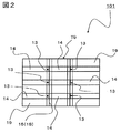
- FIG. 2 is a configuration diagram illustrating the connector 101 according to the first embodiment of the present invention, and is a top view of the connector 101 viewed from the Z1 side shown in FIG. In FIG. 2, the conductor pattern 14 is not hatched but is hatched for easy explanation.
- FIG. 3 is a configuration diagram illustrating the connector 101 according to the first embodiment of the present invention, and is a side view of the connector 101 viewed from the Y2 side shown in FIG. FIG.
- FIG. 4 is a configuration diagram illustrating the connector 101 according to the first embodiment of the present invention
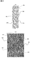
- FIG. 4A is a schematic cross-sectional view of the magnetic sheet 15 in the Q portion shown in FIG. (B) is an example of a cross-sectional SEM photograph of the magnetic sheet 15.
- FIG. 5 is a cross-sectional SEM photograph compared with the cross-sectional SEM photograph of the magnetic sheet 15 shown in FIG. 4B, and is an example in which the flat magnetic powder M5 is not oriented in the in-plane direction PD of the sheet.
- the connector 101 of the first embodiment of the present invention includes a conductor terminal 13 that is electrically connected to a pin conductor terminal 513 (shown by a broken line in FIG. 3) of the mating connector 501, A base 19 provided with a conductor pattern 14 electrically connected to the conductor terminal 13 is provided.
- the conductor terminal 13 is formed on the outer edge of the convex protruding portion T9 provided on the base 19, and the conductor terminals 13 are respectively formed on the outer sides of the two opposing surfaces of the protruding portion T9. Are provided, and each conductor terminal 13 is electrically connected to the conductor pattern 14.
- the conductor terminal 13 and the conductor pattern 14 are formed on the base 19 at the same time, and can be obtained, for example, by plating with a material such as copper using photolithography.
- the base 19 is composed of a plate-like magnetic sheet 15 made of a synthetic resin material containing magnetic powder, and the magnetic sheet 15 is heated and softened to form the protruding portion T9.
- the conductor terminal 13 and the conductor pattern 14 are formed on the magnetic material sheet 15 (base 19) in advance.
- the magnetic material sheet 15 can be preferentially arrange
- the magnetic material sheet 15 was heated and softened to form the protruding portion T9, the protruding portion T9 of the magnetic material sheet 15 can be easily manufactured.
- the two opposing conductor terminals 13 of the projecting portion T ⁇ b> 9 abut against the pin conductor terminal 513 of the mating connector 501. Electrically connected.
- the protruding portion T9 formed of the magnetic sheet 15 is formed so that the two opposing surfaces are substantially parallel to each other, and the protruding direction of the protruding portion T9 is The six conductor terminals 13 are formed in the same direction as the longitudinal direction.
- the conductor terminal 13 of the connector 101 of 1st Embodiment of this invention is formed in three places on the single side
- the magnetic sheet 15 is composed of a synthetic resin P5 such as ABS (acrylonitrile butadiene styrene) or PP (polypropylene), and a flat magnetic powder M5. Further, the magnetic sheet 15 has a plurality of flat magnetic powders M5 in a matrix of the synthetic resin P5 such that the longitudinal direction of the flat magnetic powder M5 is aligned with a desired direction in the in-plane direction PD of the magnetic sheet 15. Are aligned so as to be aligned.
- a synthetic resin P5 such as ABS (acrylonitrile butadiene styrene) or PP (polypropylene)
- PP polypropylene
- the orientation HD as used herein refers to a state in which the average inclination angle of the plurality of flat magnetic powders M5 is 45 ° or less, preferably 10 ° or less with respect to the in-plane direction PD of the magnetic sheet 15. ing.
- the inclination angle of the plurality of flat magnetic powders M5 shown in FIG. 5 is the direction ND having an angle of 45 ° or more
- the longitudinal direction of the flat magnetic powder M5 is a plurality of in-plane directions PD of the magnetic sheet 15. It cannot be said that the flat magnetic powder M5 is oriented HD so as to be arranged.
- the magnetizations of the plurality of flat magnetic powders M5 are oriented in a desired direction in the in-plane direction PD of the magnetic sheet 15, and the direction of the magnetic field of the magnetic sheet 15 is aligned in the desired direction. It becomes like this. As a result, characteristics such as thermal conversion or reflection of electromagnetic field energy are improved, and the performance of shielding electromagnetic waves (noise) is improved.
- the plurality of flat magnetic powders M5 are arranged so that the magnetic sheet 15 forming the protruding portion T9 is substantially parallel to the longitudinal direction of the six conductor terminals 13.
- the longitudinal direction of the flat magnetic powder M5 is substantially parallel to the longitudinal direction of the six conductor terminals 13 with respect to the six conductor terminals 13 respectively disposed on the outside of the protrusion T9. They are aligned and oriented. Accordingly, the magnetic field of the magnetic sheet 15 can be preferentially aligned in the longitudinal direction of the conductor terminal 13, so that the electromagnetic wave emitted from the conductor terminal 13 or entering the conductor terminal 13 is transmitted by the magnetic sheet 15. Can be shielded.
- the conductor terminals 13 are provided on the two opposing surfaces of the projecting portion T9 formed of the magnetic sheet 15 containing the flat magnetic powder M5, the magnetic sheet 15 is provided with respect to the conductor terminals 13 on both sides. Is arranged along. As a result, the electromagnetic waves coming out of the conductor terminals 13 on both sides or entering the conductor terminals 13 can be further shielded by the magnetic sheet 15 disposed along the conductor terminals, and the connector 101 with better EMC performance can be provided.
- the pin conductor terminals 513 of the mating connector 501 are disposed so as to sandwich the two opposing surfaces of the protruding portion T9.
- the magnetic material sheet 15 is arranged along the pin conductor terminals 513 on both sides.
- the wiring direction of the conductor pattern 14 and the in-plane direction PD of the magnetic material sheet 15 are substantially parallel to each other.
- the plurality of flat magnetic powders M5 of the body sheet 15 are arranged and oriented so that the longitudinal directions thereof are substantially parallel.
- the connector 101 according to the first embodiment of the present invention is obtained by attaching a wiring pattern (not shown) on one side of the printed wiring board 401 and the conductor pattern 14 by soldering HD. It is fixed to. Further, the protruding portion T9 is inserted into the hole provided in the printed wiring board 401 so as to be connected to the mating connector 501.
- the printed wiring board 401 is provided with a locking structure for locking the mating connector 501 with the mating connector 501 when the mating connector 501 is fitted to the connector 101.
- a magnetic powder is prepared by a water atomization method using a material containing iron as a main component, for example, permalloy (Fe—Ni alloy).
- a material containing iron as a main component for example, permalloy (Fe—Ni alloy).
- permalloy Fe—Ni alloy
- the conditions normally performed according to the kind of raw material can be used.
- the magnetic powder is processed into a flat shape using an apparatus such as a planetary stirring ball mill. If necessary, the flat magnetic powder M5 processed into a flat shape may be annealed for the purpose of relaxing internal stress.
- a mixed liquid (slurry) comprising the synthetic resin P5 constituting the magnetic sheet 15 and the flat magnetic powder M5 is supplied to the doctor blade device, and the base material (carrier tape) is drawn,
- the mixed solution is applied to the substrate with a predetermined thickness by a blade.
- the magnetic material sheet 15 comprised from the synthetic resin P5 and the flat magnetic powder M5 on a base material is obtained by heating.
- the magnetic sheet 15 may be used together with the base material.
- the magnetic material sheet 15 is applied to the connector 101 according to the first embodiment of the present invention by removing the base material for ease of processing. did.
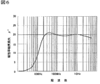
- FIG. 6 is a graph showing the frequency characteristics of the magnetic susceptibility magnetic loss ⁇ ′′ of the magnetic material sheet 15 used in the connector 101 of the first embodiment of the present invention. The frequency is shown on the horizontal axis. The measurement was performed by placing the magnetic sheet 15 on a printed wiring board (PCB) provided with a microstrip line and detecting the input value and output value of the signal with a network analyzer.
- PCB printed wiring board
- the magnetic loss magnetic loss ⁇ ′′ of the magnetic sheet 15 is 15 or more in the frequency range of 20 Mhz to 1 Ghz.
- the magnetic material sheet 15 can shield the electromagnetic waves (noise) on the high frequency side, which is a problem in communication devices and various electronic devices that handle high frequency signals.
- the connector 101 according to the first embodiment of the present invention can be suitably used for a connector of a communication device or various electronic devices that handle a high-frequency signal.
- a method for manufacturing the connector 101 will be described.
- a plating film such as copper is formed on the entire surface of one side of the magnetic sheet 15 (base 19) by electroless plating or electrolytic plating.
- a resist layer having a pattern of the conductor terminals 13 and the conductor pattern 14 is formed on the plating film, and the plating film is etched using the patterned resist layer as a mask. Thereafter, by removing the resist layer remaining on the plating film, the magnetic sheet 15 in which the conductor terminals 13 and the conductor patterns 14 are formed on one side of the magnetic sheet 15 is obtained.
- the magnetic sheet 15 is softened by heating and bent to form a U-shape to produce a protrusion T9. Accordingly, the magnetic sheet 15 that shields the electromagnetic wave that exits from the conductor terminal 13 or enters the conductor terminal 13 is easily disposed preferentially along the conductor terminal 13 in the longitudinal direction of the conductor terminal 13. Can do.
- the molding uses a vacuum molding method in which the magnetic sheet 15 is sucked from the bending mold side and the magnetic sheet 15 is brought into close contact with the mold.
- the protrusion T9 with good dimensional accuracy can be obtained, so that the electromagnetic wave absorption characteristics for absorbing electromagnetic waves in the protrusion T9 formed of the magnetic sheet 15 can be stabilized.
- the magnetic sheet 15 is formed from a thermoplastic synthetic resin P5 such as ABS (acrylonitrile butadiene styrene) or PP (polypropylene), the magnetic sheet 15 is heated and softened to form the protrusion T9. Can be easily formed. As a result, the manufacturing cost of the connector 101 with better EMC performance can be reduced.
- a thermoplastic synthetic resin P5 such as ABS (acrylonitrile butadiene styrene) or PP (polypropylene
- the connector 101 of the present invention is a flat magnetic powder of the magnetic sheet 15 that is preferentially oriented in the longitudinal direction of the conductor terminal 13 on the convex protrusion T9 on which the conductor terminal 13 is formed. Since it has M5, the direction of the magnetic field of the magnetic sheet 15 can be preferentially aligned in the longitudinal direction of the conductor terminal 13. As a result, the electromagnetic wave that exits from the conductor terminal 13 or enters the conductor terminal 13 can be shielded by the magnetic sheet 15, and a connector with good EMC performance can be provided.
- the conductor terminals 13 are provided on the two opposing surfaces of the projecting portion T9 formed of the magnetic sheet 15 containing the flat magnetic powder M5, the magnetic sheet 15 is provided with respect to the conductor terminals 13 on both sides. Is arranged along. Thereby, the electromagnetic wave which comes out of the conductor terminal 13 of both sides, or enters the conductor terminal 13 can be shielded more by the magnetic material sheet 15 arrange
- the magnetic material sheet 15 is heated and softened and bent to form a U-shaped projection T9, so that the electromagnetic wave coming out of the conductor terminal 13 or entering the conductor terminal 13 is shielded.
- the magnetic sheet 15 can be easily disposed preferentially in the longitudinal direction of the conductor terminal 13 and along the conductor terminal 13. This makes it possible to easily shield electromagnetic waves coming out of the conductor terminals 13 or entering the conductor terminals 13 and provide a connector with better EMC performance.
- the molding uses a vacuum molding method in which the magnetic sheet 15 is sucked from the bending mold side and the magnetic sheet 15 is brought into close contact with the mold, so that the projection T9 with high dimensional accuracy is used. Can be obtained. For this reason, the orientation of the flat magnetic powder M5 with magnetization of the magnetic sheet 15 can be made better with respect to the conductor terminal 13, and the electromagnetic wave absorption characteristics for absorbing electromagnetic waves at the protruding portion T9 can be stabilized. it can. As a result, the electromagnetic wave coming out of the conductor terminal 13 or entering the conductor terminal 13 can be further shielded by the magnetic sheet 15, and a connector with better EMC performance can be provided.
- the magnetic sheet 15 is formed from a thermoplastic synthetic resin P5 such as ABS (acrylonitrile butadiene styrene) or PP (polypropylene), the magnetic sheet 15 is heated and softened to form the protrusion T9. Can be easily formed. As a result, the manufacturing cost of a connector with better EMC performance can be reduced.
- a thermoplastic synthetic resin P5 such as ABS (acrylonitrile butadiene styrene) or PP (polypropylene
- the magnetic loss magnetic loss ⁇ ′′ of the magnetic material sheet 15 is 15 or more in the frequency range from 20 Mhz to 1 Ghz. Therefore, high-frequency electromagnetic waves (which are problematic in communication devices and various electronic devices that handle high-frequency signals) Therefore, it can be suitably used for connectors of communication devices that handle high-frequency signals and various electronic devices.
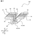
- FIG. 7 is a perspective view illustrating the connector 102 according to the second embodiment of the present invention.
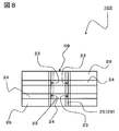
- FIG. 8 is a configuration diagram illustrating the connector 102 according to the second embodiment of the present invention, and is a top view of the connector 102 viewed from the Z1 side shown in FIG. In FIG. 8, in order to facilitate the explanation, the conductor pattern 24 is hatched although it is not a cross section.
- FIG. 9 is a configuration diagram illustrating the connector 102 according to the second embodiment of the present invention, and is a side view of the connector 102 viewed from the Y2 side shown in FIG.
- the connector 102 according to the second embodiment is different from the first embodiment in that a concave recess R9 is provided in the base 29.
- symbol is attached
- the connector 102 includes a conductor terminal 23 electrically connected to a pin conductor terminal 523 (shown by a broken line in FIG. 9) of the mating connector 502, as shown in FIGS.
- a base 29 having a conductor pattern 24 electrically connected to the conductor terminal 23 is provided.
- the conductor terminal 23 is formed on the inner edge of the concave recess R9 provided in the base 29, and the conductor terminal 23 is respectively located inside the two opposing surfaces of the recess R9.
- Each conductor terminal 23 is electrically connected to the conductor pattern 24.
- the conductor terminal 23 and the conductor pattern 24 are formed on the base 29 at the same time, and can be obtained, for example, by plating with a material such as copper using photolithography.
- the substrate 29 is composed of a magnetic sheet 25 made of a synthetic resin material containing magnetic powder, and the magnetic sheet 25 is heated and softened to form the recess R9.
- the conductor terminal 23 and the conductor pattern 24 are previously formed on the magnetic sheet 25 (base 29).
- the magnetic material sheet 25 can be preferentially arrange
- the magnetic material sheet 25 was heat-softened and the hollow part R9 was shape
- the two opposing conductor terminals 23 of the recess R ⁇ b> 9 abut against the pin conductor terminal 523 of the mating connector 502. Electrically connected.
- the recess R9 formed by the magnetic sheet 25 is formed so that the two opposing surfaces are substantially parallel to each other.
- the conductor terminals 23 are formed so that their longitudinal directions are in the same direction (the U portion and the V portion in FIG. 9).
- the conductor terminal 23 of the connector 102 of 2nd Embodiment of this invention is formed in two places on the single side
- the magnetic sheet 25 is composed of a synthetic resin P5 such as ABS (acrylonitrile butadiene styrene) or PP (polypropylene) and a flat magnetic powder M5, similarly to the magnetic sheet 15 of the first embodiment shown in FIG.
- the magnetic sheet 25 has a shape in which the longitudinal direction of the flat magnetic powder M ⁇ b> 5 is aligned with a desired direction in the in-plane direction PD of the magnetic sheet 25 in the matrix of the synthetic resin P ⁇ b> 5.
- the plurality of flat magnetic powders M5 are oriented so as to be arranged.
- the plurality of flat magnetic powders M5 are arranged so that the magnetic sheet 25 forming the recess R9 is substantially parallel to the longitudinal direction of the four conductor terminals 23.
- the longitudinal direction of the flat magnetic powder M5 is substantially parallel to the longitudinal direction of the four conductor terminals 23 with respect to the four conductor terminals 23 respectively disposed inside the recess R9. They are aligned and oriented.
- the direction of the magnetic field of the magnetic material sheet 25 can be preferentially aligned in the longitudinal direction of the conductor terminal 23, so that the electromagnetic wave emitted from the conductor terminal 23 or entering the conductor terminal 23 is Can be shielded.
- the conductor terminal 23 is provided in two surfaces which the hollow part R9 formed of the magnetic material sheet 25 containing the flat magnetic powder M5 opposes, the magnetic material sheet 25 is provided with respect to the conductor terminals 23 on both sides. Is arranged along. As a result, the electromagnetic wave coming out of the conductor terminals 23 on both sides or entering the conductor terminals 23 can be further shielded by the magnetic sheet 25 arranged along the conductor terminals, and the connector 102 with better EMC performance can be provided.
- the connector 102 according to the second embodiment of the present invention is obtained by attaching a wiring pattern (not shown) on one side of the printed wiring board 402 and the conductor pattern 24 by soldering HD. It is fixed to. Further, the opening side of the recess R9 is opposed to the hole provided in the printed wiring board 402 so as to be connected to the mating connector 502.
- the printed wiring board 402 is provided with a locking structure for locking the mating connector 502 with the mating connector 502 when the mating connector 502 is fitted to the connector 102.
- the flat magnetic powder M5 of the magnetic sheet 25 that is preferentially oriented in the longitudinal direction of the conductor terminal 23 in the concave recess R9 in which the conductor terminal 23 is formed. Therefore, the direction of the magnetic field of the magnetic material sheet 25 can be preferentially aligned in the longitudinal direction of the conductor terminal 23. As a result, the electromagnetic wave coming out of the conductor terminal 23 or entering the conductor terminal 23 can be shielded by the magnetic sheet 25, and a connector with good EMC performance can be provided.
- the conductor terminal 23 is provided in two surfaces which the hollow part R9 formed of the magnetic material sheet 25 containing the flat magnetic powder M5 opposes, the magnetic material sheet 25 is provided with respect to the conductor terminals 23 on both sides. Is arranged along. Thereby, the electromagnetic wave which comes out of the conductor terminal 23 of both sides, or enters the conductor terminal 23 can be shielded more by the magnetic material sheet 25 arranged along, and a connector with better EMC performance can be provided.
- FIG. 10 is a diagram for explaining a modification of the connector 101 according to the first embodiment of the present invention.
- FIG. 10 (a) is a side view of Modification 1 compared with the side view shown in FIG.
- FIG.10 (b) is a side view of the modification 2 compared with the side view shown in FIG.
- FIG. 11 is a diagram for explaining a modification of the connector 101 according to the first embodiment of the present invention.
- FIG. 11A is a side view of the modification 3 compared with the side view shown in FIG.
- FIG.11 (b) is a side view of the modification 4 compared with the side view shown in FIG.
- the plate-like magnetic sheet 15 is used as the base 19 and the magnetic sheet 15 is heated and softened to form the protruding portion T9.
- a plate-like magnetic material sheet C15 may be provided only on the protruding portion TC19.
- the present invention can also be applied to the hollow portion R9 of the second embodiment, and a plate-like magnetic material sheet may be provided only in the hollow portion.
- the plate-like magnetic sheet 15 is used as the base 19 and the magnetic sheet 15 is heated and softened to form the protruding portion T9.
- the film-like magnetic sheet C25 is heated and softened to form a convex protrusion TC29, which is adhered to the base C29 having the same convex shape.
- An integrated configuration may be used.
- the present invention can also be applied to the recess R9 of the second embodiment.
- the film-like magnetic sheet is heated and softened to form a concave recess, and is bonded to a substrate having the same concave shape.
- An integrated configuration may be used.
- the magnetic sheet 15 (base 19) on which the conductor terminals 13 and the conductor patterns 14 are formed is used.
- the conductor terminals 13 and the conductor patterns are formed.
- a flexible wiring board (FPC) FC3 is formed on the magnetic sheet C35 (base 19) obtained by forming a convex protrusion TC39 by heating and softening the magnetic sheet C35. It is also possible to adopt a configuration in which these are bonded and integrated.
- the present invention can also be applied to the recess R9 of the second embodiment, and a flexible wiring board (FPC) is bonded and integrated to a magnetic sheet formed by heating and softening a magnetic sheet to form a concave recess. You may make it the structure made to.
- FPC flexible wiring board
- a convex bending process is performed on one magnetic sheet 15, but as shown in FIG. 11B, the bending process is performed by stacking a plurality of magnetic sheets C45. It may be the process.
- the magnetic material sheet C45 shown in FIG.11 (b) is three sheets, it is not restricted to three sheets. According to this, since a plurality of magnetic sheets C45 are processed to form the protruding portion TC49, the thickness of the magnetic sheet C45 that shields electromagnetic waves that exit from the conductor terminals 13 or enter the conductor terminals 13 is easily increased.
- the magnetic sheet C45 can be arranged along the conductor terminal 13. As a result, the electromagnetic wave coming out of the conductor terminal 13 or entering the conductor terminal 13 can be further shielded by the magnetic sheet C45, and the connector C04 with better EMC performance can be provided.
- the concave bending may be formed by a process in which a plurality of magnetic sheets are stacked and the same effects as described above can be obtained.
- the conductor terminal (13 or 23) and the conductor pattern (14 or 24) are previously formed on the magnetic sheet (15 or 25) before the convex or concave bending process.
- the step of forming the conductor terminal and the conductor pattern on the magnetic sheet may be used.
Landscapes
- Engineering & Computer Science (AREA)
- Microelectronics & Electronic Packaging (AREA)
- Details Of Connecting Devices For Male And Female Coupling (AREA)
- Coupling Device And Connection With Printed Circuit (AREA)
- Manufacturing Of Electrical Connectors (AREA)
- Shielding Devices Or Components To Electric Or Magnetic Fields (AREA)
Abstract
【課題】電磁波を吸収または反射して遮蔽する材料として扁平状の磁性粉末を用いた場合に、扁平状の磁性粉末の並びが一定にならないので、EMC性能が場所によってばらつく等の従来例のようなコネクタに対して、EMC性能の良いコネクタを提供することを目的とする。【解決手段】相手側コネクタのピン導体端子と電気的に接続する導体端子(13)と、導体端子(13)と電気的に接続する導体パターン(14)とが設けられた基体(19)とを備えて構成されたコネクタ(101)において、導体端子(13)は、基体(19)に設けられた凹状の窪み部若しくは凸状の突出部に形成され、窪み部若しくは突出部は、扁平状磁性粉末を含有した合成樹脂からなるフィルム状若しくは板状の磁性体シート(15)を有しており、扁平状磁性粉末は、磁性体シート(15)の面内方向に配向されるとともに、導体端子(13)の長手方向に向けて優先的に配向されていることを特徴とした。
Description
本発明は、各種電子機器或いは回路基板間をつなぐコネクタに関し、特に、各種電子機器から発生する不用な電磁波を低減することができるコネクタに関する。
通信機器や各種電子機器からの電磁波が、外部に放射されたり伝送されたりすることで、外部及び内部干渉による機器自体の誤動作などの問題が大きくなってきている。特に、最近の通信技術、デジタル技術の進歩及び信号の高速化に伴い、高周波数側のノイズが問題となってきている。このような不要電磁波の発生、漏洩、相互干渉による誤動作への対策として、ノイズ発生源にシールドを施す方法やノイズの伝送線路にノイズフィルタ等を挿入する方法がとられている。最近では、コネクタから出る或いはコネクタに入る電磁波によるEMI(Electro Magnetic Interference)が問題となってきており、コネクタに対してEMC(Electro Magnetic Compatibility)性能が求められてきている。
コネクタに対するEMI対策の従来技術として、特許文献1では、図12に示すように、信号伝送や通信時等に発生する不要な電磁波の漏洩を吸収し得る電子機器間のコネクタ800が提案されている。図12に示すコネクタ800は、接続ケーブル811の先端に設けられたコネクタハウジング802と、接続ケーブル811内の複数本の伝送線(図示せず)と配線接続されているコネクタピン803とから構成されている。そして、コネクタハウジング802の外側に電磁波吸収材805を塗布し固化させるか(図12に示した従来例)、コネクタハウジング802内に電磁波吸収材805を充填させるか、電磁波吸収材805を含有した合成樹脂材を成形加工してコネクタハウジング802とするかの手段を用いて、安価にして不要な電磁波を効率よく吸収できるコネクタが得られるとしている。特に、電磁界エネルギーを熱変換、或いは反射させる等の特性を利用して吸収する電磁波吸収特性を有する電磁波吸収材805として、扁平状に加工された軟磁性体の磁性粉末を用いており、例えば、三菱マテリアル株式会社製の不繊布型電波吸収材“エミクロス”(商品名)が好適であるとしている。
また、上述した従来例1の箱形に形成されたコネクタハウジング802を有しないタイプとして、特許文献2では、図13に示すように、ベース樹脂板920の一部を突出させた凸部922に導体パターン924を形成して、プリント配線板とワイヤーハーネスと接続するためのコネクタ900が提案されている。この従来例2のコネクタ900は、従来例1に見られる筐体(コネクタハウジング802)がないので、シールド部材を配置することが難しい。それ故、コネクタ900には、シールド対策は施されていない。
従来例1のように、電磁波を吸収または反射して遮蔽する材料として、扁平状の磁性粉末を用いた場合、扁平状の磁性粉末の並びの方向を揃えて、磁化の配向を揃えることがEMC性能の向上に有効であると一般的に知られている。しかしながら、従来例1のような方法では、扁平状の磁性粉末の並びの方向を揃える工夫がなされていないか或いは難しいかで、扁平状の磁性粉末の並びが一定にならないので、扁平状の磁性粉末の磁化の配向が揃えられないと言う問題があった。したがって、EMC性能が場所によってばらつく等、EMC性能の良いコネクタが得られないという課題があった。
また、従来例2のような構成では、シールド部材を配置することが難しく、ノイズの伝送線路にノイズフィルタ等の新たな電子部品を挿入する方法を取らなければいけない。
本発明は、上述した課題を解決するもので、EMC性能の良いコネクタを提供することを目的とする。
本発明は、上述した課題を解決するもので、EMC性能の良いコネクタを提供することを目的とする。
この課題を解決するために、本発明の請求項1によるコネクタは、相手側コネクタのピン導体端子と電気的に接続する導体端子と、前記導体端子と電気的に接続する導体パターンとが設けられた基体とを備えて構成されたコネクタにおいて、前記導体端子は、前記基体に設けられた凹状の窪み部若しくは凸状の突出部に形成され、前記窪み部若しくは前記突出部は、扁平状磁性粉末を含有した合成樹脂からなるフィルム状若しくは板状の磁性体シートを有しており、前記扁平状磁性粉末は、前記磁性体シートの面内方向に配向されるとともに、前記導体端子の長手方向に向けて優先的に配向されていることを特徴としている。
また、本発明の請求項2によるコネクタは、前記窪み部若しくは前記突出部の対向する2面に前記導体端子が設けられていることを特徴としている。
また、本発明の請求項3によるコネクタは、前記窪み部若しくは前記突出部が、前記磁性体シートを加熱軟化させて成形し、前記窪み部若しくは前記突出部としたことを特徴としている。
また、本発明の請求項4によるコネクタは、前記成形が、前記磁性体シートを型側から吸引し、前記型に前記磁性体シートを密着させて行う真空成形であることを特徴としている。
また、本発明の請求項5によるコネクタは、前記成形が、前記磁性体シートを重ねて加工したことを特徴としている。
また、本発明の請求項6によるコネクタは、前記磁性体シートの樹脂が、熱可塑性の合成樹脂からなることを特徴としている。
また、本発明の請求項7によるコネクタは、前記磁性体シートの磁性率磁気損失が、周波数で20Mhzから1Ghzの範囲において、15以上であることを特徴としている。
請求項1の発明によれば、本発明のコネクタは、導体端子が形成された凹状の窪み部若しくは凸状の突出部に、導体端子の長手方向に向けて優先的に配向されている磁性体シートの扁平状磁性粉末を有しているので、この磁性体シートの磁界の向きを導体端子の長手方向に向けて優先的に揃えることができる。このことにより、導体端子から出る或いは導体端子に入る電磁波を磁性体シートで遮蔽することができ、EMC性能の良いコネクタを提供できる。
請求項2の発明によれば、本発明のコネクタは、扁平状磁性粉末を含有した磁性体シートを有した窪み部若しくは突出部の対向する2面に、導体端子が設けられているので、両側の導体端子に対して磁性体シートが沿うように配置される。このことにより、両側の導体端子から出る或いは導体端子に入る電磁波を、沿うように配置された磁性体シートでより遮蔽することができ、EMC性能のより良いコネクタを提供できる。
請求項3の発明によれば、本発明のコネクタは、磁性体シートを加熱軟化させて成形し、窪み部若しくは突出部としたので、導体端子から出る或いは導体端子に入る電磁波を遮蔽する磁性体シートを、導体端子の長手方向に向けて優先的に及び導体端子に沿うように容易に配置することができる。このことにより、導体端子から出る或いは導体端子に入る電磁波を容易に遮蔽することができ、EMC性能のより良いコネクタを提供できる。
請求項4の発明によれば、本発明のコネクタは、磁性体シートを真空成形で成形し、窪み部若しくは突出部としたので、寸法精度の良い部若しくは突出部を得ることができる。このため、導体端子に対して、磁性体シートの磁化の扁平状磁性粉末の配向をより良い配向とすることができ、電磁波を吸収する電磁波吸収特性を安定させることができる。このことにより、導体端子から出る或いは導体端子に入る電磁波を磁性体シートでより一層遮蔽することができ、EMC性能のより一層良いコネクタを提供できる。
請求項5の発明によれば、本発明のコネクタは、磁性体シートを重ねて加工し、窪み部若しくは突出部としたので、導体端子から出る或いは導体端子に入る電磁波を遮蔽する磁性体シートの厚みを容易に増やして、導体端子に沿うように磁性体シートを配置することができる。このことにより、導体端子から出る或いは導体端子に入る電磁波を磁性体シートでより一層遮蔽することができ、EMC性能のより一層良いコネクタを提供できる。
請求項6の発明によれば、本発明のコネクタは、磁性体シートが熱可塑性の合成樹脂から形成されているので、磁性体シートを加熱軟化させて成形し、窪み部若しくは突出部を容易に成形できる。このことにより、EMC性能のより良いコネクタの製造コストを低減することができる。
請求項7の発明によれば、本発明のコネクタは、磁性体シートの磁性率磁気損失が、周波数で20Mhzから1Ghzの範囲において、15以上であるので、高周波の信号を扱う通信機器や各種電子機器において問題となる高周波側の電磁波(ノイズ)を遮蔽することができる。このことにより、高周波の信号を扱う通信機器や各種電子機器のコネクタに好適に用いることができる。
したがって、本発明のコネクタは、EMC性能の良いコネクタを提供できる。
したがって、本発明のコネクタは、EMC性能の良いコネクタを提供できる。
以下、本発明の実施の形態について添付図面を参照して詳細に説明する。
[第1実施形態]
図1は、本発明の第1実施形態のコネクタ101を説明する斜視図である。図2は、本発明の第1実施形態のコネクタ101を説明する構成図であって、図1に示すZ1側から見たコネクタ101の上面図である。なお、図2には、説明を容易にするため、導体パターン14に、断面では無いがハッチングを入れている。図3は、本発明の第1実施形態のコネクタ101を説明する構成図であって、図1に示すY2側から見たコネクタ101の側面図である。図4は、本発明の第1実施形態のコネクタ101を説明する構成図であって、図4(a)は、図3に示すQ部分の磁性体シート15の断面模式図であり、図4(b)は、磁性体シート15の断面SEM写真の一例である。図5は、図4(b)に示した磁性体シート15の断面SEM写真と比較した断面SEM写真であって、扁平状磁性粉末M5がシートの面内方向PDに配向されない一例である。
[第1実施形態]
図1は、本発明の第1実施形態のコネクタ101を説明する斜視図である。図2は、本発明の第1実施形態のコネクタ101を説明する構成図であって、図1に示すZ1側から見たコネクタ101の上面図である。なお、図2には、説明を容易にするため、導体パターン14に、断面では無いがハッチングを入れている。図3は、本発明の第1実施形態のコネクタ101を説明する構成図であって、図1に示すY2側から見たコネクタ101の側面図である。図4は、本発明の第1実施形態のコネクタ101を説明する構成図であって、図4(a)は、図3に示すQ部分の磁性体シート15の断面模式図であり、図4(b)は、磁性体シート15の断面SEM写真の一例である。図5は、図4(b)に示した磁性体シート15の断面SEM写真と比較した断面SEM写真であって、扁平状磁性粉末M5がシートの面内方向PDに配向されない一例である。
本発明の第1実施形態のコネクタ101は、図1ないし図3に示すように、相手側コネクタ501のピン導体端子513(図3の破線で示す)と電気的に接続する導体端子13と、導体端子13と電気的に接続する導体パターン14とが設けられた基体19とを備えて構成される。
導体端子13は、図1及び図3に示すように、基体19に設けられた凸状の突出部T9の外縁に形成されており、突出部T9の対向する2面の外側にそれぞれ導体端子13が設けられ、それぞれの導体端子13が導体パターン14と電気的に接続されている。導体端子13と導体パターン14とは、基体19に同時に形成され、例えば、フォトリソグラフィーを用い、銅等の材質のめっきを施すことによって得られる。
基体19は、磁性粉末を含有した合成樹脂材からなる板状の磁性体シート15で構成され、磁性体シート15を加熱軟化させて、突出部T9を成形している。突出部T9を形成する前には、予め導体端子13及び導体パターン14を磁性体シート15(基体19)に形成しておく。このため、突出部T9を磁性体シート15で形成したので、突出部T9に成形された導体端子13の長手方向に向けて、磁性体シート15を優先的に配置することができる。また、磁性体シート15を加熱軟化させて突出部T9を成形したので、磁性体シート15の突出部T9を容易に作製することができる。
また、図3に示すように、相手側コネクタ501がコネクタ101に嵌合された際に、突出部T9の対向する2面の導体端子13は、相手側コネクタ501のピン導体端子513と当接し、電気的に接続される。また、図1及び図3に示すように、磁性体シート15で形成された突出部T9は、対向する2面が略平行になるように形成されており、突出部T9の凸状の方向と6個の導体端子13の長手方向とが、同じ方向になるように形成されている。なお、本発明の第1実施形態のコネクタ101の導体端子13は、突出部T9の片面に3箇所形成され、両面合わせて6個であるが、6個に限るものではない。
磁性体シート15は、図4に示すように、ABS(アクリロニトリルブタジエンスチレン)、PP(ポリプロピレン)等の合成樹脂P5と、扁平状磁性粉末M5とから構成される。また、磁性体シート15は、合成樹脂P5のマトリックスに、扁平状磁性粉末M5の長手方向が磁性体シート15の面内方向PDの所望の方向に揃えた形で、複数の扁平状磁性粉末M5を並べるように配向HDさせている。ここで言う配向HDとは、複数の扁平状磁性粉末M5の平均傾き角度が磁性体シート15の面内方向PDに対して、45°以下の状態を指し、好ましくは10°以下の状態を指している。図5に示す複数の扁平状磁性粉末M5の傾き角度が45°以上の角度の方向NDの場合、扁平状磁性粉末M5の長手方向が磁性体シート15の面内方向PDに対して、複数の扁平状磁性粉末M5を並べるように配向HDさせているとは言えない。
このようにして、複数の扁平状磁性粉末M5の磁化が磁性体シート15の面内方向PDの所望の方向に配向するようになり、磁性体シート15の磁界の向きが、所望の方向に揃うようになる。このことにより、電磁界エネルギーを熱変換、或いは反射させる等の特性が向上し、電磁波(ノイズ)を遮蔽する性能が向上する。
そして、複数の扁平状磁性粉末M5は、この突出部T9を形成している磁性体シート15が、6個の導体端子13の長手方向に対して、略平行になるように配置されているので、突出部T9の外側にそれぞれ配設された6個の導体端子13に対して、扁平状磁性粉末M5の長手方向が6個の導体端子13の長手方向に対して略平行になるように、並べられ配向するようになる。このことにより、この磁性体シート15の磁界の向きを導体端子13の長手方向に向けて優先的に揃えることができるので、導体端子13から出る或いは導体端子13に入る電磁波を磁性体シート15で遮蔽することができる。
このようにして、扁平状磁性粉末M5の長手方向が磁性体シート15の面内方向PDの所望の方向に揃えられた磁性体シート15を突出部T9とした構成を採用したので、従来例1のような電磁波吸収材805を塗布し固化させる方法等と比較して、容易に、磁性体シート15の磁界の向きを導体端子13の長手方向に向けて優先的に揃えることができる。また、従来例2のようなシールド部材を配置することが難しい構造であっても、導体端子13に対して磁性体シート15を配置することができる。
また、扁平状磁性粉末M5を含有した磁性体シート15で形成された突出部T9の対向する2面に、導体端子13が設けられているので、両側の導体端子13に対して磁性体シート15が沿うように配置される。このことにより、両側の導体端子13から出る或いは導体端子13に入る電磁波を、沿うように配置された磁性体シート15でより遮蔽することができ、EMC性能のより良いコネクタ101を提供できる。
また、図3に示すように、相手側コネクタ501がコネクタ101に嵌合された際に、突出部T9の対向する2面を挟むように相手側コネクタ501のピン導体端子513が配置されるので、両側のピン導体端子513に対して磁性体シート15が沿うように配置される。このことにより、両側のピン導体端子513から出る或いはピン導体端子513に入る電磁波を、沿うように配置された磁性体シート15で遮蔽することができ、EMC性能のより一層良いコネクタ101を提供できる。
また、図3に示すQ部分、R部分及びS部分は、導体パターン14の配線方向と磁性体シート15の面内方向PDとが略平行になっているので、導体パターン14に対して、磁性体シート15の複数の扁平状磁性粉末M5の長手方向が略平行になるように、並べられ配向するようになる。このことにより、導体パターン14から出る或いは導体パターン14に入る電磁波を、略平行に配置された磁性体シート15で遮蔽することができ、EMC性能のより一層良いコネクタ101を提供できる。
本発明の第1実施形態のコネクタ101は、図3に示すように、プリント配線板401の片側の配線パターン(図示していない)と導体パターン14をはんだHD付けすることにより、プリント配線板401に固定している。また、プリント配線板401に設けられた孔部に突出部T9を挿通して、相手側コネクタ501と接続するようにしている。なお、プリント配線板401には、図示していないが、相手側コネクタ501がコネクタ101に嵌合された際に、相手側コネクタ501と係止させるための係止構造が設けられている。
次に、本発明の第1実施形態のコネクタ101の製造方法について説明する。
最初に、磁性体シート15の製造方法について説明する。まず、鉄を主成分とする材料、例えばパーマロイ(Fe-Ni合金)を用い、水アトマイズ法により磁性粉末を作製する。なお、水アトマイズ法に限定されず、ガスアトマイズ法、上記合金溶湯から急冷したリボンを粉砕して粉末化する液体急冷法等を用いても良い。また、水アトマイズ法、ガスアトマイズ法、液体急冷法の処理条件については、原料の種類に応じて通常行われる条件を用いることが出来る。そして、得られた磁性粉末を分級して粒度を揃えた後に、遊星撹拌型ボールミル等の装置を用いて、磁性粉末を扁平状に加工する。なお、必要に応じて、内部応力を緩和させる目的で、扁平状に加工された扁平状磁性粉末M5にアニール処理を施しても良い。
最初に、磁性体シート15の製造方法について説明する。まず、鉄を主成分とする材料、例えばパーマロイ(Fe-Ni合金)を用い、水アトマイズ法により磁性粉末を作製する。なお、水アトマイズ法に限定されず、ガスアトマイズ法、上記合金溶湯から急冷したリボンを粉砕して粉末化する液体急冷法等を用いても良い。また、水アトマイズ法、ガスアトマイズ法、液体急冷法の処理条件については、原料の種類に応じて通常行われる条件を用いることが出来る。そして、得られた磁性粉末を分級して粒度を揃えた後に、遊星撹拌型ボールミル等の装置を用いて、磁性粉末を扁平状に加工する。なお、必要に応じて、内部応力を緩和させる目的で、扁平状に加工された扁平状磁性粉末M5にアニール処理を施しても良い。
次に、磁性体シート15を構成する合成樹脂P5と、扁平状磁性粉末M5とを有して成る混合液(スラリー)を、ドクターブレード装置に供給し、基材(キャリアテープ)を引きながら、ブレードにより混合液を所定厚さで基材上に塗布する。そして、加熱することにより、基材上に合成樹脂P5と扁平状磁性粉末M5とから構成される磁性体シート15が得られる。なお、磁性体シート15は、この基材と一緒に用いても良いが、本発明の第1実施形態のコネクタ101へは、加工の容易性から、この基材を除去して、単独で適用した。
図6は、本発明の第1実施形態のコネクタ101に用いた磁性体シート15の磁性率磁気損失μ”の周波数特性を示したグラフである。縦軸に磁性率磁気損失μ”を示し、横軸に周波数を示している。測定は、マイクロストリップラインを設けたプリント配線板(PCB)に磁性体シート15を載置し、信号の入力値及び出力値をネットワークアナライザーにて検出して行った。
図6に示すように、磁性体シート15の磁性率磁気損失μ”は、周波数が20Mhzから1Ghzの範囲において、15以上である。この磁性率磁気損失μ”が大きければ大きいほど、電磁界エネルギーを熱に変換する効率が高く、ひいては電磁波を吸収する電磁波吸収特性が高くなる。このため、磁性体シート15は、高周波の信号を扱う通信機器や各種電子機器において問題となる高周波側の電磁波(ノイズ)を遮蔽することができる。このことにより、本発明の第1実施形態のコネクタ101は、高周波の信号を扱う通信機器や各種電子機器のコネクタに好適に用いることができる。
次に、コネクタ101の製造方法について説明する。先ず、磁性体シート15(基体19)の片側全面に、無電解めっき或いは電解めっきにより、銅等のめっき被膜を形成する。次に、導体端子13及び導体パターン14のパターンを有するレジスト層をめっき被膜上に形成し、パターニングされたレジスト層をマスクとしてめっき被膜をエッチングする。その後、めっき被膜上に残存したレジスト層を除去することにより、磁性体シート15の片側上に導体端子13及び導体パターン14が形成された磁性体シート15が得られる。
次に、この磁性体シート15を加熱軟化させて、曲げ加工を行うことにより、U字状に成形して突出部T9が作製される。このことにより、導体端子13から出る或いは導体端子13に入る電磁波を遮蔽する磁性体シート15を、導体端子13の長手方向に向けて優先的に及び導体端子13に沿うように容易に配置することができる。
さらに、上記成形は、磁性体シート15を曲げ加工の金型側から吸引し、金型に磁性体シート15を密着させて行う真空成形の方法を用いている。このことにより、寸法精度の良い突出部T9を得ることができるので、磁性体シート15から構成される突出部T9における電磁波を吸収する電磁波吸収特性を安定させることができる。
また、磁性体シート15が、ABS(アクリロニトリルブタジエンスチレン)、PP(ポリプロピレン)等の熱可塑性の合成樹脂P5から形成されているので、磁性体シート15を加熱軟化させて成形し、突出部T9を容易に形成できる。このことにより、EMC性能のより良いコネクタ101の製造コストを低減することができる。
以上により、本発明のコネクタ101は、導体端子13が形成された凸状の突出部T9に、導体端子13の長手方向に向けて優先的に配向されている磁性体シート15の扁平状磁性粉末M5を有しているので、この磁性体シート15の磁界の向きを導体端子13の長手方向に向けて優先的に揃えることができる。このことにより、導体端子13から出る或いは導体端子13に入る電磁波を磁性体シート15で遮蔽することができ、EMC性能の良いコネクタを提供できる。
このようにして、扁平状磁性粉末M5の長手方向が磁性体シート15の面内方向PDの所望の方向に揃えられた磁性体シート15を突出部T9とした構成を採用したので、従来例1のような電磁波吸収材805を塗布し固化させる方法等と比較して、容易に、磁性体シート15の磁界の向きを導体端子13の長手方向に向けて優先的に揃えることができる。また、従来例2のようなシールド部材を配置することが難しい構造であっても、導体端子13に対して磁性体シート15を配置することができる。
また、扁平状磁性粉末M5を含有した磁性体シート15で形成された突出部T9の対向する2面に、導体端子13が設けられているので、両側の導体端子13に対して磁性体シート15が沿うように配置される。このことにより、両側の導体端子13から出る或いは導体端子13に入る電磁波を、沿うように配置された磁性体シート15でより遮蔽することができ、EMC性能のより良いコネクタを提供できる。
また、磁性体シート15を加熱軟化させて、曲げ加工を行うことにより、U字状に成形して突出部T9が作製されるので、導体端子13から出る或いは導体端子13に入る電磁波を遮蔽する磁性体シート15を、導体端子13の長手方向に向けて優先的に及び導体端子13に沿うように容易に配置することができる。このことにより、導体端子13から出る或いは導体端子13に入る電磁波を容易に遮蔽することができ、EMC性能のより良いコネクタを提供できる。
さらに、上記成形は、磁性体シート15を曲げ加工の金型側から吸引し、金型に磁性体シート15を密着させて行う真空成形の方法を用いているので、寸法精度の良い突出部T9を得ることができる。このため、導体端子13に対して、磁性体シート15の磁化の扁平状磁性粉末M5の配向をより良い配向とすることができ、突出部T9における電磁波を吸収する電磁波吸収特性を安定させることができる。このことにより、導体端子13から出る或いは導体端子13に入る電磁波を磁性体シート15でより一層遮蔽することができ、EMC性能のより一層良いコネクタを提供できる。
また、磁性体シート15が、ABS(アクリロニトリルブタジエンスチレン)、PP(ポリプロピレン)等の熱可塑性の合成樹脂P5から形成されているので、磁性体シート15を加熱軟化させて成形し、突出部T9を容易に形成できる。このことにより、EMC性能のより良いコネクタの製造コストを低減することができる。
また、磁性体シート15の磁性率磁気損失μ”が、周波数で20Mhzから1Ghzの範囲において、15以上であるので、高周波の信号を扱う通信機器や各種電子機器において問題となる高周波側の電磁波(ノイズ)を遮蔽することができる。このことにより、高周波の信号を扱う通信機器や各種電子機器のコネクタに好適に用いることができる。
[第2実施形態]
図7は、本発明の第2実施形態のコネクタ102を説明する斜視図である。図8は、本発明の第2実施形態のコネクタ102を説明する構成図であって、図7に示すZ1側から見たコネクタ102の上面図である。なお、図8には、説明を容易にするため、導体パターン24に、断面では無いがハッチングを入れている。図9は、本発明の第2実施形態のコネクタ102を説明する構成図であって、図7に示すY2側から見たコネクタ102の側面図である。第2実施形態のコネクタ102は、第1実施形態に対し、基体29に凹状の窪み部R9を設けている点が異なる。なお、第1実施形態と同一構成については、同一符号を付して詳細な説明は省略する。
図7は、本発明の第2実施形態のコネクタ102を説明する斜視図である。図8は、本発明の第2実施形態のコネクタ102を説明する構成図であって、図7に示すZ1側から見たコネクタ102の上面図である。なお、図8には、説明を容易にするため、導体パターン24に、断面では無いがハッチングを入れている。図9は、本発明の第2実施形態のコネクタ102を説明する構成図であって、図7に示すY2側から見たコネクタ102の側面図である。第2実施形態のコネクタ102は、第1実施形態に対し、基体29に凹状の窪み部R9を設けている点が異なる。なお、第1実施形態と同一構成については、同一符号を付して詳細な説明は省略する。
本発明の第2実施形態のコネクタ102は、図7ないし図9に示すように、相手側コネクタ502のピン導体端子523(図9の破線で示す)と電気的に接続する導体端子23と、導体端子23と電気的に接続する導体パターン24とが設けられた基体29とを備えて構成される。
導体端子23は、図7及び図9に示すように、基体29に設けられた凹状の窪み部R9の内縁に形成されており、窪み部R9の対向する2面の内側にそれぞれ導体端子23が設けられ、それぞれの導体端子23が導体パターン24と電気的に接続されている。導体端子23と導体パターン24とは、基体29に同時に形成され、例えば、フォトリソグラフィーを用い、銅等の材質のめっきを施すことによって得られる。
基体29は、磁性粉末を含有した合成樹脂材からなる磁性体シート25で構成され、磁性体シート25を加熱軟化させて、窪み部R9を成形している。窪み部R9を形成する前には、予め導体端子23及び導体パターン24を磁性体シート25(基体29)に形成しておく。このため、窪み部R9を磁性体シート25で形成したので、窪み部R9に成形された導体端子23の長手方向に向けて、磁性体シート25を優先的に配置することができる。また、磁性体シート25を加熱軟化させて窪み部R9を成形したので、磁性体シート25の窪み部R9を容易に作製することができる。
また、図9に示すように、相手側コネクタ502がコネクタ102に嵌合された際に、窪み部R9の対向する2面の導体端子23は、相手側コネクタ502のピン導体端子523と当接し、電気的に接続される。また、図7及び図9に示すように、磁性体シート25で形成された窪み部R9は、対向する2面が略平行になるように形成されており、窪み部R9の凹状の方向と4個の導体端子23の長手方向とが、同じ方向になるように形成されている(図9のU部分及びV部分)。なお、本発明の第2実施形態のコネクタ102の導体端子23は、窪み部R9の片面に2箇所形成され、両面合わせて4個であるが、4個に限るものではない。
磁性体シート25は、図4に示す第1実施形態の磁性体シート15と同様に、ABS(アクリロニトリルブタジエンスチレン)、PP(ポリプロピレン)等の合成樹脂P5と、扁平状磁性粉末M5とから構成される。また、磁性体シート25は、磁性体シート15と同同様に、合成樹脂P5のマトリックスに、扁平状磁性粉末M5の長手方向が磁性体シート25の面内方向PDの所望の方向に揃えた形で、複数の扁平状磁性粉末M5を並べるように配向させている。
そして、複数の扁平状磁性粉末M5は、この窪み部R9を形成している磁性体シート25が、4個の導体端子23の長手方向に対して、略平行になるように配置されているので、窪み部R9の内側にそれぞれ配設された4個の導体端子23に対して、扁平状磁性粉末M5の長手方向が4個の導体端子23の長手方向に対して略平行になるように、並べられ配向するようになる。このことにより、この磁性体シート25の磁界の向きを導体端子23の長手方向に向けて優先的に揃えることができるので、導体端子23から出る或いは導体端子23に入る電磁波を磁性体シート25で遮蔽することができる。
このようにして、扁平状磁性粉末M5の長手方向が磁性体シート25の面内方向PDの所望の方向に揃えられた磁性体シート25を窪み部R9とした構成を採用したので、従来例1のような電磁波吸収材805を塗布し固化させる方法等と比較して、容易に、磁性体シート25の磁界の向きを導体端子23の長手方向に向けて優先的に揃えることができる。
また、扁平状磁性粉末M5を含有した磁性体シート25で形成された窪み部R9の対向する2面に、導体端子23が設けられているので、両側の導体端子23に対して磁性体シート25が沿うように配置される。このことにより、両側の導体端子23から出る或いは導体端子23に入る電磁波を、沿うように配置された磁性体シート25でより遮蔽することができ、EMC性能のより良いコネクタ102を提供できる。
本発明の第2実施形態のコネクタ102は、図9に示すように、プリント配線板402の片側の配線パターン(図示していない)と導体パターン24をはんだHD付けすることにより、プリント配線板402に固定している。また、プリント配線板402に設けられた孔部に窪み部R9の開口部側を対向させて、相手側コネクタ502と接続するようにしている。なお、プリント配線板402には、図示していないが、相手側コネクタ502がコネクタ102に嵌合された際に、相手側コネクタ502と係止させるための係止構造が設けられている。
以上により、本発明のコネクタ102は、導体端子23が形成された凹状の窪み部R9に、導体端子23の長手方向に向けて優先的に配向されている磁性体シート25の扁平状磁性粉末M5を有しているので、この磁性体シート25の磁界の向きを導体端子23の長手方向に向けて優先的に揃えることができる。このことにより、導体端子23から出る或いは導体端子23に入る電磁波を磁性体シート25で遮蔽することができ、EMC性能の良いコネクタを提供できる。
このようにして、扁平状磁性粉末M5の長手方向が磁性体シート25の面内方向PDの所望の方向に揃えられた磁性体シート25を窪み部R9とした構成を採用したので、従来例1のような電磁波吸収材805を塗布し固化させる方法等と比較して、容易に、磁性体シート25の磁界の向きを導体端子23の長手方向に向けて優先的に揃えることができる。
また、扁平状磁性粉末M5を含有した磁性体シート25で形成された窪み部R9の対向する2面に、導体端子23が設けられているので、両側の導体端子23に対して磁性体シート25が沿うように配置される。このことにより、両側の導体端子23から出る或いは導体端子23に入る電磁波を、沿うように配置された磁性体シート25でより遮蔽することができ、EMC性能のより良いコネクタを提供できる。
なお、本発明は上記実施形態に限定されるものではなく、例えば次のように変形して実施することができ、これらの実施形態も本発明の技術的範囲に属する。
図10は、本発明の第1実施形態のコネクタ101の変形例を説明する図であって、図10(a)は、図3に示す側面図と比較した変形例1の側面図であり、図10(b)は、図3に示す側面図と比較した変形例2の側面図である。図11は、本発明の第1実施形態のコネクタ101の変形例を説明する図であって、図11(a)は、図3に示す側面図と比較した変形例3の側面図であり、図11(b)は、図3に示す側面図と比較した変形例4の側面図である。
<変形例1>
上記第1実施形態では、基体19として、板状の磁性体シート15を用い、磁性体シート15を加熱軟化させて、突出部T9を成形するようにしたが、図10(a)に示すように、突出部TC19の部分のみに、板状の磁性体シートC15が設けられた構成にしても良い。同様にして、上記第2実施形態の窪み部R9にも適用でき、窪み部の部分のみに、板状の磁性体シートが設けられた構成にしても良い。
上記第1実施形態では、基体19として、板状の磁性体シート15を用い、磁性体シート15を加熱軟化させて、突出部T9を成形するようにしたが、図10(a)に示すように、突出部TC19の部分のみに、板状の磁性体シートC15が設けられた構成にしても良い。同様にして、上記第2実施形態の窪み部R9にも適用でき、窪み部の部分のみに、板状の磁性体シートが設けられた構成にしても良い。
<変形例2>
上記第1実施形態では、基体19として、板状の磁性体シート15を用い、磁性体シート15を加熱軟化させて、突出部T9を成形するようにしたが、図10(b)に示すように、フィルム状の磁性体シートC25を用い、フィルム状の磁性体シートC25を加熱軟化させて凸状の突出部TC29を成形し、同形の凸状を有した基体C29に接着し、基体C29と一体化させた構成にしても良い。同様にして、上記第2実施形態の窪み部R9にも適用でき、フィルム状の磁性体シートを加熱軟化させて凹状の窪み部を成形し、同形の凹状を有した基体に接着し、基体と一体化させた構成にしても良い。
上記第1実施形態では、基体19として、板状の磁性体シート15を用い、磁性体シート15を加熱軟化させて、突出部T9を成形するようにしたが、図10(b)に示すように、フィルム状の磁性体シートC25を用い、フィルム状の磁性体シートC25を加熱軟化させて凸状の突出部TC29を成形し、同形の凸状を有した基体C29に接着し、基体C29と一体化させた構成にしても良い。同様にして、上記第2実施形態の窪み部R9にも適用でき、フィルム状の磁性体シートを加熱軟化させて凹状の窪み部を成形し、同形の凹状を有した基体に接着し、基体と一体化させた構成にしても良い。
<変形例3>
上記第1実施形態では、導体端子13及び導体パターン14が形成された磁性体シート15(基体19)を用いた構成にしたが、図11(a)に示すように、導体端子13及び導体パターン14が形成されたフレキシブル配線板(FPC)FC3を用い、磁性体シートC35を加熱軟化させて凸状の突出部TC39を成形した磁性体シートC35(基体19)に、フレキシブル配線板(FPC)FC3を接着して一体化させた構成にしても良い。同様にして、上記第2実施形態の窪み部R9にも適用でき、磁性体シートを加熱軟化させて凹状の窪み部を成形した磁性体シートに、フレキシブル配線板(FPC)を接着して一体化させた構成にしても良い。
上記第1実施形態では、導体端子13及び導体パターン14が形成された磁性体シート15(基体19)を用いた構成にしたが、図11(a)に示すように、導体端子13及び導体パターン14が形成されたフレキシブル配線板(FPC)FC3を用い、磁性体シートC35を加熱軟化させて凸状の突出部TC39を成形した磁性体シートC35(基体19)に、フレキシブル配線板(FPC)FC3を接着して一体化させた構成にしても良い。同様にして、上記第2実施形態の窪み部R9にも適用でき、磁性体シートを加熱軟化させて凹状の窪み部を成形した磁性体シートに、フレキシブル配線板(FPC)を接着して一体化させた構成にしても良い。
<変形例4>
上記第1実施形態では、1枚の磁性体シート15に凸状の曲げ加工を行ったが、図11(b)に示すように、曲げ加工の成形が、磁性体シートC45を複数重ねて加工した工程であっても良い。なお、図11(b)に示す磁性体シートC45は3枚であるが、3枚に限るものではない。これによれば、磁性体シートC45を複数重ねて加工し、突出部TC49としたので、導体端子13から出る或いは導体端子13に入る電磁波を遮蔽する磁性体シートC45の厚みを容易に増やして、導体端子13に沿うように磁性体シートC45を配置することができる。このことにより、導体端子13から出る或いは導体端子13に入る電磁波を磁性体シートC45でより一層遮蔽することができ、EMC性能のより一層良いコネクタC04を提供できる。
上記第1実施形態では、1枚の磁性体シート15に凸状の曲げ加工を行ったが、図11(b)に示すように、曲げ加工の成形が、磁性体シートC45を複数重ねて加工した工程であっても良い。なお、図11(b)に示す磁性体シートC45は3枚であるが、3枚に限るものではない。これによれば、磁性体シートC45を複数重ねて加工し、突出部TC49としたので、導体端子13から出る或いは導体端子13に入る電磁波を遮蔽する磁性体シートC45の厚みを容易に増やして、導体端子13に沿うように磁性体シートC45を配置することができる。このことにより、導体端子13から出る或いは導体端子13に入る電磁波を磁性体シートC45でより一層遮蔽することができ、EMC性能のより一層良いコネクタC04を提供できる。
また、上記第2実施形態においても、凹状の曲げ加工の成形が、磁性体シートを複数重ねて加工した工程であっても良く、上記と同様の効果が得られる。
<変形例5>
上記実施形態では、凸状若しくは凹状の曲げ加工を行う前に、予め導体端子(13若しくは23)及び導体パターン(14若しくは24)を磁性体シート(15若しくは25)に形成しておくような工程にしたが、凸状若しくは凹状の曲げ加工を行なった後に、導体端子及び導体パターンを磁性体シートに形成する工程にしても良い。
上記実施形態では、凸状若しくは凹状の曲げ加工を行う前に、予め導体端子(13若しくは23)及び導体パターン(14若しくは24)を磁性体シート(15若しくは25)に形成しておくような工程にしたが、凸状若しくは凹状の曲げ加工を行なった後に、導体端子及び導体パターンを磁性体シートに形成する工程にしても良い。
本発明は上記実施の形態に限定されず、本発明の目的の範囲を逸脱しない限りにおいて適宜変更することが可能である。
13、23 導体端子
14、24 導体パターン
15、25、C15、C25、C35、C45 磁性体シート
R9 窪み部
19、29、C29 基体
T9、TC19、TC29、TC39 突出部
M5 扁平状磁性粉末
P5 合成樹脂
PD 面内方向
μ” 磁性率磁気損失
501 相手側コネクタ
513、523 ピン導体端子
101、102、C04 コネクタ
14、24 導体パターン
15、25、C15、C25、C35、C45 磁性体シート
R9 窪み部
19、29、C29 基体
T9、TC19、TC29、TC39 突出部
M5 扁平状磁性粉末
P5 合成樹脂
PD 面内方向
μ” 磁性率磁気損失
501 相手側コネクタ
513、523 ピン導体端子
101、102、C04 コネクタ
Claims (8)
- 相手側コネクタのピン端子と電気的に接続する導体端子と、前記導体端子と電気的に接続する導体パターンとが設けられた基体とを備えて構成されたコネクタにおいて、
前記導体端子は、前記基体に設けられた凹状の窪み部若しくは凸状の突出部に形成され、
前記窪み部若しくは前記突出部は、扁平状磁性粉末を含有した合成樹脂からなるフィルム状若しくは板状の磁性体シートを有しており、
前記扁平状磁性粉末は、前記磁性体シートの面内方向に配向されるとともに、前記導体端子の長手方向に向けて優先的に配向されていることを特徴とするコネクタ。 - 前記窪み部若しくは前記突出部の対向する2面に前記導体端子が設けられていることを特徴とする請求項1に記載のコネクタ。
- 前記窪み部若しくは前記突出部は、前記磁性体シートを加熱軟化させて成形し、前記窪み部若しくは前記突出部としたことを特徴とする請求項2に記載のコネクタ。
- 前記成形は、前記磁性体シートを型側から吸引し、前記型に前記磁性体シートを密着させて行う真空成形であることを特徴とする請求項3に記載のコネクタ。
- 前記成形は、前記磁性体シートを重ねて加工したことを特徴とする請求項3に記載のコネクタ。
- 前記成形は、前記磁性体シートを重ねて加工したことを特徴とする請求項4に記載のコネクタ。
- 前記磁性体シートの樹脂は、熱可塑性の合成樹脂からなることを特徴とする請求項3に記載のコネクタ。
- 前記磁性体シートの磁性率磁気損失は、周波数が20Mhzから1Ghzの範囲において、15以上であることを特徴とする請求項1に記載のコネクタ。
Applications Claiming Priority (2)
| Application Number | Priority Date | Filing Date | Title |
|---|---|---|---|
| JP2011087295A JP2014132514A (ja) | 2011-04-11 | 2011-04-11 | コネクタ |
| JP2011-087295 | 2011-04-11 |
Publications (1)
| Publication Number | Publication Date |
|---|---|
| WO2012140949A1 true WO2012140949A1 (ja) | 2012-10-18 |
Family
ID=47009133
Family Applications (1)
| Application Number | Title | Priority Date | Filing Date |
|---|---|---|---|
| PCT/JP2012/053427 Ceased WO2012140949A1 (ja) | 2011-04-11 | 2012-02-14 | コネクタ |
Country Status (2)
| Country | Link |
|---|---|
| JP (1) | JP2014132514A (ja) |
| WO (1) | WO2012140949A1 (ja) |
Citations (5)
| Publication number | Priority date | Publication date | Assignee | Title |
|---|---|---|---|---|
| JPH088001A (ja) * | 1994-06-17 | 1996-01-12 | Yazaki Corp | プリント配線板の回路接続方法 |
| JPH1140981A (ja) * | 1997-07-22 | 1999-02-12 | Tokin Corp | 複合磁性テープとそれを用いたノイズ対策方法 |
| JP2001210924A (ja) * | 2000-01-27 | 2001-08-03 | Tdk Corp | 複合磁性成型物、電子部品、複合磁性組成物および製造方法 |
| WO2003041474A1 (fr) * | 2001-11-09 | 2003-05-15 | Tdk Corporation | Element magnetique composite, feuille absorbant les ondes electromagnetiques, procede de production d'un article en feuille, et procede de production d'une feuille absorbant les ondes electromagnetiques |
| JP2007123373A (ja) * | 2005-10-26 | 2007-05-17 | Tdk Corp | ノイズ対策用複合磁性シート積層体及びその装着方法 |
-
2011
- 2011-04-11 JP JP2011087295A patent/JP2014132514A/ja not_active Withdrawn
-
2012
- 2012-02-14 WO PCT/JP2012/053427 patent/WO2012140949A1/ja not_active Ceased
Patent Citations (5)
| Publication number | Priority date | Publication date | Assignee | Title |
|---|---|---|---|---|
| JPH088001A (ja) * | 1994-06-17 | 1996-01-12 | Yazaki Corp | プリント配線板の回路接続方法 |
| JPH1140981A (ja) * | 1997-07-22 | 1999-02-12 | Tokin Corp | 複合磁性テープとそれを用いたノイズ対策方法 |
| JP2001210924A (ja) * | 2000-01-27 | 2001-08-03 | Tdk Corp | 複合磁性成型物、電子部品、複合磁性組成物および製造方法 |
| WO2003041474A1 (fr) * | 2001-11-09 | 2003-05-15 | Tdk Corporation | Element magnetique composite, feuille absorbant les ondes electromagnetiques, procede de production d'un article en feuille, et procede de production d'une feuille absorbant les ondes electromagnetiques |
| JP2007123373A (ja) * | 2005-10-26 | 2007-05-17 | Tdk Corp | ノイズ対策用複合磁性シート積層体及びその装着方法 |
Also Published As
| Publication number | Publication date |
|---|---|
| JP2014132514A (ja) | 2014-07-17 |
Similar Documents
| Publication | Publication Date | Title |
|---|---|---|
| JP6376230B2 (ja) | 電子回路パッケージ | |
| EP1788666B1 (en) | Interconnection system with improved high frequency performance | |
| JP5988004B1 (ja) | 電子回路パッケージ | |
| JP6328698B2 (ja) | 電子回路パッケージ | |
| KR101070778B1 (ko) | 자성 복합 분말, 이의 제조방법 및 이를 포함하는 전자파 노이즈 억제 필름 | |
| CN208095043U (zh) | 电磁屏蔽膜及线路板 | |
| KR20000064305A (ko) | 자성 수지침투 가공재와 그 제조방법 및 그를 이용한 프린트배선기판 | |
| US20140210131A1 (en) | Electromagnetic noise suppression sheet, flat cable for high-frequency signals, flexible printed circuit board, and process for producing the electromagnetic noise suppression sheet | |
| CN116096561A (zh) | 电磁波屏蔽膜及屏蔽印制线路板 | |
| CN205811027U (zh) | 高频信号传输线路 | |
| WO2012140949A1 (ja) | コネクタ | |
| JPH1084195A5 (ja) | ||
| JP5872801B2 (ja) | インターポーザ | |
| WO2012140947A1 (ja) | コネクタ | |
| WO2015074580A1 (zh) | 薄膜天线结构及其制造方法 | |
| WO2014132610A1 (ja) | 配線基板、半導体装置、プリント基板及び配線基板の製造方法 | |
| WO2012140948A1 (ja) | コネクタ | |
| JP4446585B2 (ja) | 樹脂複合体及びこれを用いた放射雑音抑制基板 | |
| CN212259433U (zh) | 一种高频高速电路板 | |
| KR100755775B1 (ko) | 전자기파 노이즈 억제 필름 및 그의 제조방법 | |
| JP2000249873A (ja) | 電子回路一体型光伝送モジュール及びその製造方法 | |
| JPH1187980A (ja) | 複合磁性シート | |
| WO2008026247A1 (en) | Electromagnetic wave shield structure and formation method thereof | |
| CN119626658A (zh) | 一种抗电磁波干扰的数据线及其制备方法 | |
| JP5139750B2 (ja) | 多層プリント配線基板 |
Legal Events
| Date | Code | Title | Description |
|---|---|---|---|
| 121 | Ep: the epo has been informed by wipo that ep was designated in this application |
Ref document number: 12771773 Country of ref document: EP Kind code of ref document: A1 |
|
| NENP | Non-entry into the national phase |
Ref country code: DE |
|
| 122 | Ep: pct application non-entry in european phase |
Ref document number: 12771773 Country of ref document: EP Kind code of ref document: A1 |
|
| NENP | Non-entry into the national phase |
Ref country code: JP |