WO2012140786A1 - 電極用ペースト組成物、太陽電池素子及び太陽電池 - Google Patents
電極用ペースト組成物、太陽電池素子及び太陽電池 Download PDFInfo
- Publication number
- WO2012140786A1 WO2012140786A1 PCT/JP2011/060471 JP2011060471W WO2012140786A1 WO 2012140786 A1 WO2012140786 A1 WO 2012140786A1 JP 2011060471 W JP2011060471 W JP 2011060471W WO 2012140786 A1 WO2012140786 A1 WO 2012140786A1
- Authority
- WO
- WIPO (PCT)
- Prior art keywords
- electrode
- particles
- mass
- paste composition
- solar cell
- Prior art date
Links
- 239000000203 mixture Substances 0.000 title claims abstract description 178
- 239000002003 electrode paste Substances 0.000 title claims abstract description 152
- 239000002245 particle Substances 0.000 claims abstract description 314
- 239000011521 glass Substances 0.000 claims abstract description 112
- OAICVXFJPJFONN-UHFFFAOYSA-N Phosphorus Chemical compound [P] OAICVXFJPJFONN-UHFFFAOYSA-N 0.000 claims abstract description 108
- 229910052698 phosphorus Inorganic materials 0.000 claims abstract description 108
- 239000011574 phosphorus Substances 0.000 claims abstract description 108
- 229910000881 Cu alloy Inorganic materials 0.000 claims abstract description 92
- ATJFFYVFTNAWJD-UHFFFAOYSA-N Tin Chemical compound [Sn] ATJFFYVFTNAWJD-UHFFFAOYSA-N 0.000 claims abstract description 88
- 239000002904 solvent Substances 0.000 claims abstract description 36
- 229920005989 resin Polymers 0.000 claims abstract description 35
- 239000011347 resin Substances 0.000 claims abstract description 35
- 229910052718 tin Inorganic materials 0.000 claims description 89
- 229910052710 silicon Inorganic materials 0.000 claims description 78
- XUIMIQQOPSSXEZ-UHFFFAOYSA-N Silicon Chemical compound [Si] XUIMIQQOPSSXEZ-UHFFFAOYSA-N 0.000 claims description 75
- 239000010703 silicon Substances 0.000 claims description 75
- 239000000758 substrate Substances 0.000 claims description 74
- 238000010304 firing Methods 0.000 claims description 57
- BQCADISMDOOEFD-UHFFFAOYSA-N Silver Chemical compound [Ag] BQCADISMDOOEFD-UHFFFAOYSA-N 0.000 claims description 46
- 229910052709 silver Inorganic materials 0.000 claims description 45
- 239000004332 silver Substances 0.000 claims description 45
- 229910017755 Cu-Sn Inorganic materials 0.000 claims description 25
- 229910017927 Cu—Sn Inorganic materials 0.000 claims description 25
- 229910000905 alloy phase Inorganic materials 0.000 claims description 25
- KUNSUQLRTQLHQQ-UHFFFAOYSA-N copper tin Chemical compound [Cu].[Sn] KUNSUQLRTQLHQQ-UHFFFAOYSA-N 0.000 claims description 25
- 229910001128 Sn alloy Inorganic materials 0.000 claims description 18
- 238000002425 crystallisation Methods 0.000 claims description 8
- 230000008025 crystallization Effects 0.000 claims description 8
- 229910009042 Sn—P—O Inorganic materials 0.000 claims 1
- 239000010949 copper Substances 0.000 description 44
- RYGMFSIKBFXOCR-UHFFFAOYSA-N Copper Chemical group [Cu] RYGMFSIKBFXOCR-UHFFFAOYSA-N 0.000 description 39
- 229910052802 copper Inorganic materials 0.000 description 39
- 238000000034 method Methods 0.000 description 38
- 230000003647 oxidation Effects 0.000 description 32
- 238000007254 oxidation reaction Methods 0.000 description 32
- 238000009792 diffusion process Methods 0.000 description 28
- 229910052782 aluminium Inorganic materials 0.000 description 24
- XAGFODPZIPBFFR-UHFFFAOYSA-N aluminium Chemical compound [Al] XAGFODPZIPBFFR-UHFFFAOYSA-N 0.000 description 21
- 230000000052 comparative effect Effects 0.000 description 21
- 229910045601 alloy Inorganic materials 0.000 description 20
- 239000000956 alloy Substances 0.000 description 20
- 238000010438 heat treatment Methods 0.000 description 19
- 238000007639 printing Methods 0.000 description 16
- 230000015572 biosynthetic process Effects 0.000 description 15
- 238000000605 extraction Methods 0.000 description 15
- 238000004519 manufacturing process Methods 0.000 description 13
- 239000012298 atmosphere Substances 0.000 description 12
- 230000004907 flux Effects 0.000 description 12
- 230000008569 process Effects 0.000 description 12
- VYPSYNLAJGMNEJ-UHFFFAOYSA-N Silicium dioxide Chemical compound O=[Si]=O VYPSYNLAJGMNEJ-UHFFFAOYSA-N 0.000 description 11
- GNTDGMZSJNCJKK-UHFFFAOYSA-N divanadium pentaoxide Chemical compound O=[V](=O)O[V](=O)=O GNTDGMZSJNCJKK-UHFFFAOYSA-N 0.000 description 11
- 239000004065 semiconductor Substances 0.000 description 10
- KFZMGEQAYNKOFK-UHFFFAOYSA-N Isopropanol Chemical compound CC(C)O KFZMGEQAYNKOFK-UHFFFAOYSA-N 0.000 description 9
- 125000004429 atom Chemical group 0.000 description 9
- 238000006243 chemical reaction Methods 0.000 description 9
- 239000000463 material Substances 0.000 description 9
- 238000010248 power generation Methods 0.000 description 9
- 239000001856 Ethyl cellulose Substances 0.000 description 7
- ZZSNKZQZMQGXPY-UHFFFAOYSA-N Ethyl cellulose Chemical compound CCOCC1OC(OC)C(OCC)C(OCC)C1OC1C(O)C(O)C(OC)C(CO)O1 ZZSNKZQZMQGXPY-UHFFFAOYSA-N 0.000 description 7
- 229920001249 ethyl cellulose Polymers 0.000 description 7
- 235000019325 ethyl cellulose Nutrition 0.000 description 7
- 238000002844 melting Methods 0.000 description 7
- 230000008018 melting Effects 0.000 description 7
- 239000000843 powder Substances 0.000 description 7
- WUOACPNHFRMFPN-UHFFFAOYSA-N alpha-terpineol Chemical compound CC1=CCC(C(C)(C)O)CC1 WUOACPNHFRMFPN-UHFFFAOYSA-N 0.000 description 6
- SQIFACVGCPWBQZ-UHFFFAOYSA-N delta-terpineol Natural products CC(C)(O)C1CCC(=C)CC1 SQIFACVGCPWBQZ-UHFFFAOYSA-N 0.000 description 6
- 229910052751 metal Inorganic materials 0.000 description 6
- 239000002184 metal Substances 0.000 description 6
- 238000007650 screen-printing Methods 0.000 description 6
- PUZPDOWCWNUUKD-UHFFFAOYSA-M sodium fluoride Chemical compound [F-].[Na+] PUZPDOWCWNUUKD-UHFFFAOYSA-M 0.000 description 6
- 229940116411 terpineol Drugs 0.000 description 6
- 229910018072 Al 2 O 3 Inorganic materials 0.000 description 5
- 229910052581 Si3N4 Inorganic materials 0.000 description 5
- 229910004298 SiO 2 Inorganic materials 0.000 description 5
- XLOMVQKBTHCTTD-UHFFFAOYSA-N Zinc monoxide Chemical compound [Zn]=O XLOMVQKBTHCTTD-UHFFFAOYSA-N 0.000 description 5
- 229910052700 potassium Inorganic materials 0.000 description 5
- 239000000376 reactant Substances 0.000 description 5
- 239000000377 silicon dioxide Substances 0.000 description 5
- 235000012239 silicon dioxide Nutrition 0.000 description 5
- HQVNEWCFYHHQES-UHFFFAOYSA-N silicon nitride Chemical compound N12[Si]34N5[Si]62N3[Si]51N64 HQVNEWCFYHHQES-UHFFFAOYSA-N 0.000 description 5
- 229910015902 Bi 2 O 3 Inorganic materials 0.000 description 4
- UQSXHKLRYXJYBZ-UHFFFAOYSA-N Iron oxide Chemical compound [Fe]=O UQSXHKLRYXJYBZ-UHFFFAOYSA-N 0.000 description 4
- JKWMSGQKBLHBQQ-UHFFFAOYSA-N diboron trioxide Chemical compound O=BOB=O JKWMSGQKBLHBQQ-UHFFFAOYSA-N 0.000 description 4
- 230000000694 effects Effects 0.000 description 4
- 238000011156 evaluation Methods 0.000 description 4
- 238000001704 evaporation Methods 0.000 description 4
- 230000008020 evaporation Effects 0.000 description 4
- AMWRITDGCCNYAT-UHFFFAOYSA-L hydroxy(oxo)manganese;manganese Chemical compound [Mn].O[Mn]=O.O[Mn]=O AMWRITDGCCNYAT-UHFFFAOYSA-L 0.000 description 4
- XMGQYMWWDOXHJM-UHFFFAOYSA-N limonene Chemical compound CC(=C)C1CCC(C)=CC1 XMGQYMWWDOXHJM-UHFFFAOYSA-N 0.000 description 4
- 229910052744 lithium Inorganic materials 0.000 description 4
- PQXKHYXIUOZZFA-UHFFFAOYSA-M lithium fluoride Chemical compound [Li+].[F-] PQXKHYXIUOZZFA-UHFFFAOYSA-M 0.000 description 4
- 238000002156 mixing Methods 0.000 description 4
- NROKBHXJSPEDAR-UHFFFAOYSA-M potassium fluoride Chemical compound [F-].[K+] NROKBHXJSPEDAR-UHFFFAOYSA-M 0.000 description 4
- 150000005846 sugar alcohols Polymers 0.000 description 4
- 229910052721 tungsten Inorganic materials 0.000 description 4
- ZWEHNKRNPOVVGH-UHFFFAOYSA-N 2-Butanone Chemical compound CCC(C)=O ZWEHNKRNPOVVGH-UHFFFAOYSA-N 0.000 description 3
- CSCPPACGZOOCGX-UHFFFAOYSA-N Acetone Chemical compound CC(C)=O CSCPPACGZOOCGX-UHFFFAOYSA-N 0.000 description 3
- 229910001152 Bi alloy Inorganic materials 0.000 description 3
- QPLDLSVMHZLSFG-UHFFFAOYSA-N Copper oxide Chemical compound [Cu]=O QPLDLSVMHZLSFG-UHFFFAOYSA-N 0.000 description 3
- ZMXDDKWLCZADIW-UHFFFAOYSA-N N,N-Dimethylformamide Chemical compound CN(C)C=O ZMXDDKWLCZADIW-UHFFFAOYSA-N 0.000 description 3
- LRHPLDYGYMQRHN-UHFFFAOYSA-N N-Butanol Chemical compound CCCCO LRHPLDYGYMQRHN-UHFFFAOYSA-N 0.000 description 3
- HEMHJVSKTPXQMS-UHFFFAOYSA-M Sodium hydroxide Chemical compound [OH-].[Na+] HEMHJVSKTPXQMS-UHFFFAOYSA-M 0.000 description 3
- YXFVVABEGXRONW-UHFFFAOYSA-N Toluene Chemical compound CC1=CC=CC=C1 YXFVVABEGXRONW-UHFFFAOYSA-N 0.000 description 3
- 230000002378 acidificating effect Effects 0.000 description 3
- 229920000180 alkyd Polymers 0.000 description 3
- 229910052787 antimony Inorganic materials 0.000 description 3
- 229910052788 barium Inorganic materials 0.000 description 3
- QVQLCTNNEUAWMS-UHFFFAOYSA-N barium oxide Chemical compound [Ba]=O QVQLCTNNEUAWMS-UHFFFAOYSA-N 0.000 description 3
- 229910052790 beryllium Inorganic materials 0.000 description 3
- 238000005219 brazing Methods 0.000 description 3
- 229910052793 cadmium Inorganic materials 0.000 description 3
- 229910052791 calcium Inorganic materials 0.000 description 3
- 239000011575 calcium Substances 0.000 description 3
- 229940028356 diethylene glycol monobutyl ether Drugs 0.000 description 3
- 239000006185 dispersion Substances 0.000 description 3
- 238000001035 drying Methods 0.000 description 3
- 239000007772 electrode material Substances 0.000 description 3
- 229910052737 gold Inorganic materials 0.000 description 3
- 229910052745 lead Inorganic materials 0.000 description 3
- 239000007788 liquid Substances 0.000 description 3
- 229910052749 magnesium Inorganic materials 0.000 description 3
- 239000011777 magnesium Substances 0.000 description 3
- 229910052750 molybdenum Inorganic materials 0.000 description 3
- VLKZOEOYAKHREP-UHFFFAOYSA-N n-Hexane Chemical compound CCCCCC VLKZOEOYAKHREP-UHFFFAOYSA-N 0.000 description 3
- 229910052759 nickel Inorganic materials 0.000 description 3
- TWNQGVIAIRXVLR-UHFFFAOYSA-N oxo(oxoalumanyloxy)alumane Chemical compound O=[Al]O[Al]=O TWNQGVIAIRXVLR-UHFFFAOYSA-N 0.000 description 3
- JCGNDDUYTRNOFT-UHFFFAOYSA-N oxolane-2,4-dione Chemical compound O=C1COC(=O)C1 JCGNDDUYTRNOFT-UHFFFAOYSA-N 0.000 description 3
- YEXPOXQUZXUXJW-UHFFFAOYSA-N oxolead Chemical compound [Pb]=O YEXPOXQUZXUXJW-UHFFFAOYSA-N 0.000 description 3
- 230000000149 penetrating effect Effects 0.000 description 3
- 238000002360 preparation method Methods 0.000 description 3
- 238000006722 reduction reaction Methods 0.000 description 3
- 229910052708 sodium Inorganic materials 0.000 description 3
- 239000011734 sodium Substances 0.000 description 3
- 239000011775 sodium fluoride Substances 0.000 description 3
- 235000013024 sodium fluoride Nutrition 0.000 description 3
- 229910052712 strontium Inorganic materials 0.000 description 3
- 239000000126 substance Substances 0.000 description 3
- 150000003505 terpenes Chemical class 0.000 description 3
- 235000007586 terpenes Nutrition 0.000 description 3
- YLQBMQCUIZJEEH-UHFFFAOYSA-N tetrahydrofuran Natural products C=1C=COC=1 YLQBMQCUIZJEEH-UHFFFAOYSA-N 0.000 description 3
- 229910052716 thallium Inorganic materials 0.000 description 3
- 229910052719 titanium Inorganic materials 0.000 description 3
- 239000010936 titanium Substances 0.000 description 3
- 229910052720 vanadium Inorganic materials 0.000 description 3
- 238000009692 water atomization Methods 0.000 description 3
- 229910052725 zinc Inorganic materials 0.000 description 3
- 239000011701 zinc Substances 0.000 description 3
- 229910052726 zirconium Inorganic materials 0.000 description 3
- GRWFGVWFFZKLTI-IUCAKERBSA-N (-)-α-pinene Chemical compound CC1=CC[C@@H]2C(C)(C)[C@H]1C2 GRWFGVWFFZKLTI-IUCAKERBSA-N 0.000 description 2
- 239000004925 Acrylic resin Substances 0.000 description 2
- 229920000178 Acrylic resin Polymers 0.000 description 2
- IJGRMHOSHXDMSA-UHFFFAOYSA-N Atomic nitrogen Chemical compound N#N IJGRMHOSHXDMSA-UHFFFAOYSA-N 0.000 description 2
- ZOXJGFHDIHLPTG-UHFFFAOYSA-N Boron Chemical compound [B] ZOXJGFHDIHLPTG-UHFFFAOYSA-N 0.000 description 2
- 239000005751 Copper oxide Substances 0.000 description 2
- 229910017518 Cu Zn Inorganic materials 0.000 description 2
- 229910017752 Cu-Zn Inorganic materials 0.000 description 2
- 229910017943 Cu—Zn Inorganic materials 0.000 description 2
- RTZKZFJDLAIYFH-UHFFFAOYSA-N Diethyl ether Chemical compound CCOCC RTZKZFJDLAIYFH-UHFFFAOYSA-N 0.000 description 2
- IAZDPXIOMUYVGZ-UHFFFAOYSA-N Dimethylsulphoxide Chemical compound CS(C)=O IAZDPXIOMUYVGZ-UHFFFAOYSA-N 0.000 description 2
- ZLMJMSJWJFRBEC-UHFFFAOYSA-N Potassium Chemical compound [K] ZLMJMSJWJFRBEC-UHFFFAOYSA-N 0.000 description 2
- 229910017910 Sb—Zn Inorganic materials 0.000 description 2
- 235000021355 Stearic acid Nutrition 0.000 description 2
- WYURNTSHIVDZCO-UHFFFAOYSA-N Tetrahydrofuran Chemical compound C1CCOC1 WYURNTSHIVDZCO-UHFFFAOYSA-N 0.000 description 2
- RIRXDDRGHVUXNJ-UHFFFAOYSA-N [Cu].[P] Chemical compound [Cu].[P] RIRXDDRGHVUXNJ-UHFFFAOYSA-N 0.000 description 2
- 239000000654 additive Substances 0.000 description 2
- GHPGOEFPKIHBNM-UHFFFAOYSA-N antimony(3+);oxygen(2-) Chemical compound [O-2].[O-2].[O-2].[Sb+3].[Sb+3] GHPGOEFPKIHBNM-UHFFFAOYSA-N 0.000 description 2
- QVGXLLKOCUKJST-UHFFFAOYSA-N atomic oxygen Chemical compound [O] QVGXLLKOCUKJST-UHFFFAOYSA-N 0.000 description 2
- 230000004888 barrier function Effects 0.000 description 2
- UAHWPYUMFXYFJY-UHFFFAOYSA-N beta-myrcene Chemical compound CC(C)=CCCC(=C)C=C UAHWPYUMFXYFJY-UHFFFAOYSA-N 0.000 description 2
- 229910000416 bismuth oxide Inorganic materials 0.000 description 2
- 229910052796 boron Inorganic materials 0.000 description 2
- CXKCTMHTOKXKQT-UHFFFAOYSA-N cadmium oxide Inorganic materials [Cd]=O CXKCTMHTOKXKQT-UHFFFAOYSA-N 0.000 description 2
- CFEAAQFZALKQPA-UHFFFAOYSA-N cadmium(2+);oxygen(2-) Chemical compound [O-2].[Cd+2] CFEAAQFZALKQPA-UHFFFAOYSA-N 0.000 description 2
- ULDHMXUKGWMISQ-UHFFFAOYSA-N carvone Chemical compound CC(=C)C1CC=C(C)C(=O)C1 ULDHMXUKGWMISQ-UHFFFAOYSA-N 0.000 description 2
- 239000012461 cellulose resin Substances 0.000 description 2
- 238000002485 combustion reaction Methods 0.000 description 2
- 150000001875 compounds Chemical class 0.000 description 2
- 238000007796 conventional method Methods 0.000 description 2
- 229910000431 copper oxide Inorganic materials 0.000 description 2
- SWXVUIWOUIDPGS-UHFFFAOYSA-N diacetone alcohol Chemical compound CC(=O)CC(C)(C)O SWXVUIWOUIDPGS-UHFFFAOYSA-N 0.000 description 2
- TYIXMATWDRGMPF-UHFFFAOYSA-N dibismuth;oxygen(2-) Chemical compound [O-2].[O-2].[O-2].[Bi+3].[Bi+3] TYIXMATWDRGMPF-UHFFFAOYSA-N 0.000 description 2
- 235000014113 dietary fatty acids Nutrition 0.000 description 2
- XBDQKXXYIPTUBI-UHFFFAOYSA-N dimethylselenoniopropionate Natural products CCC(O)=O XBDQKXXYIPTUBI-UHFFFAOYSA-N 0.000 description 2
- YWEUIGNSBFLMFL-UHFFFAOYSA-N diphosphonate Chemical compound O=P(=O)OP(=O)=O YWEUIGNSBFLMFL-UHFFFAOYSA-N 0.000 description 2
- POULHZVOKOAJMA-UHFFFAOYSA-N dodecanoic acid Chemical compound CCCCCCCCCCCC(O)=O POULHZVOKOAJMA-UHFFFAOYSA-N 0.000 description 2
- 239000003759 ester based solvent Substances 0.000 description 2
- 238000005530 etching Methods 0.000 description 2
- 239000004210 ether based solvent Substances 0.000 description 2
- 239000000194 fatty acid Substances 0.000 description 2
- 229930195729 fatty acid Natural products 0.000 description 2
- 150000004665 fatty acids Chemical class 0.000 description 2
- 238000011049 filling Methods 0.000 description 2
- IPCSVZSSVZVIGE-UHFFFAOYSA-N hexadecanoic acid Chemical compound CCCCCCCCCCCCCCCC(O)=O IPCSVZSSVZVIGE-UHFFFAOYSA-N 0.000 description 2
- MRELNEQAGSRDBK-UHFFFAOYSA-N lanthanum(3+);oxygen(2-) Chemical compound [O-2].[O-2].[O-2].[La+3].[La+3] MRELNEQAGSRDBK-UHFFFAOYSA-N 0.000 description 2
- HTUMBQDCCIXGCV-UHFFFAOYSA-N lead oxide Chemical compound [O-2].[Pb+2] HTUMBQDCCIXGCV-UHFFFAOYSA-N 0.000 description 2
- 239000000395 magnesium oxide Substances 0.000 description 2
- CPLXHLVBOLITMK-UHFFFAOYSA-N magnesium oxide Inorganic materials [Mg]=O CPLXHLVBOLITMK-UHFFFAOYSA-N 0.000 description 2
- AXZKOIWUVFPNLO-UHFFFAOYSA-N magnesium;oxygen(2-) Chemical compound [O-2].[Mg+2] AXZKOIWUVFPNLO-UHFFFAOYSA-N 0.000 description 2
- QIQXTHQIDYTFRH-UHFFFAOYSA-N octadecanoic acid Chemical compound CCCCCCCCCCCCCCCCCC(O)=O QIQXTHQIDYTFRH-UHFFFAOYSA-N 0.000 description 2
- OQCDKBAXFALNLD-UHFFFAOYSA-N octadecanoic acid Natural products CCCCCCCC(C)CCCCCCCCC(O)=O OQCDKBAXFALNLD-UHFFFAOYSA-N 0.000 description 2
- 229910052760 oxygen Inorganic materials 0.000 description 2
- 239000001301 oxygen Substances 0.000 description 2
- FDPIMTJIUBPUKL-UHFFFAOYSA-N pentan-3-one Chemical compound CCC(=O)CC FDPIMTJIUBPUKL-UHFFFAOYSA-N 0.000 description 2
- 230000000704 physical effect Effects 0.000 description 2
- 229920002037 poly(vinyl butyral) polymer Polymers 0.000 description 2
- 239000011591 potassium Substances 0.000 description 2
- 239000011698 potassium fluoride Substances 0.000 description 2
- 235000003270 potassium fluoride Nutrition 0.000 description 2
- 230000009257 reactivity Effects 0.000 description 2
- 230000009467 reduction Effects 0.000 description 2
- 238000007789 sealing Methods 0.000 description 2
- 239000003566 sealing material Substances 0.000 description 2
- NDVLTYZPCACLMA-UHFFFAOYSA-N silver oxide Chemical compound [O-2].[Ag+].[Ag+] NDVLTYZPCACLMA-UHFFFAOYSA-N 0.000 description 2
- 238000005245 sintering Methods 0.000 description 2
- 229910000679 solder Inorganic materials 0.000 description 2
- 239000008117 stearic acid Substances 0.000 description 2
- DLYUQMMRRRQYAE-UHFFFAOYSA-N tetraphosphorus decaoxide Chemical compound O1P(O2)(=O)OP3(=O)OP1(=O)OP2(=O)O3 DLYUQMMRRRQYAE-UHFFFAOYSA-N 0.000 description 2
- WUUHFRRPHJEEKV-UHFFFAOYSA-N tripotassium borate Chemical compound [K+].[K+].[K+].[O-]B([O-])[O-] WUUHFRRPHJEEKV-UHFFFAOYSA-N 0.000 description 2
- YHQGMYUVUMAZJR-UHFFFAOYSA-N α-terpinene Chemical compound CC(C)C1=CC=C(C)CC1 YHQGMYUVUMAZJR-UHFFFAOYSA-N 0.000 description 2
- WTARULDDTDQWMU-RKDXNWHRSA-N (+)-β-pinene Chemical compound C1[C@H]2C(C)(C)[C@@H]1CCC2=C WTARULDDTDQWMU-RKDXNWHRSA-N 0.000 description 1
- WTARULDDTDQWMU-IUCAKERBSA-N (-)-Nopinene Natural products C1[C@@H]2C(C)(C)[C@H]1CCC2=C WTARULDDTDQWMU-IUCAKERBSA-N 0.000 description 1
- LNAZSHAWQACDHT-XIYTZBAFSA-N (2r,3r,4s,5r,6s)-4,5-dimethoxy-2-(methoxymethyl)-3-[(2s,3r,4s,5r,6r)-3,4,5-trimethoxy-6-(methoxymethyl)oxan-2-yl]oxy-6-[(2r,3r,4s,5r,6r)-4,5,6-trimethoxy-2-(methoxymethyl)oxan-3-yl]oxyoxane Chemical compound CO[C@@H]1[C@@H](OC)[C@H](OC)[C@@H](COC)O[C@H]1O[C@H]1[C@H](OC)[C@@H](OC)[C@H](O[C@H]2[C@@H]([C@@H](OC)[C@H](OC)O[C@@H]2COC)OC)O[C@@H]1COC LNAZSHAWQACDHT-XIYTZBAFSA-N 0.000 description 1
- DAFHKNAQFPVRKR-UHFFFAOYSA-N (3-hydroxy-2,2,4-trimethylpentyl) 2-methylpropanoate Chemical compound CC(C)C(O)C(C)(C)COC(=O)C(C)C DAFHKNAQFPVRKR-UHFFFAOYSA-N 0.000 description 1
- GQVMHMFBVWSSPF-SOYUKNQTSA-N (4E,6E)-2,6-dimethylocta-2,4,6-triene Chemical compound C\C=C(/C)\C=C\C=C(C)C GQVMHMFBVWSSPF-SOYUKNQTSA-N 0.000 description 1
- WUOACPNHFRMFPN-SECBINFHSA-N (S)-(-)-alpha-terpineol Chemical compound CC1=CC[C@@H](C(C)(C)O)CC1 WUOACPNHFRMFPN-SECBINFHSA-N 0.000 description 1
- SCYULBFZEHDVBN-UHFFFAOYSA-N 1,1-Dichloroethane Chemical compound CC(Cl)Cl SCYULBFZEHDVBN-UHFFFAOYSA-N 0.000 description 1
- LGXVIGDEPROXKC-UHFFFAOYSA-N 1,1-dichloroethene Chemical group ClC(Cl)=C LGXVIGDEPROXKC-UHFFFAOYSA-N 0.000 description 1
- BGJSXRVXTHVRSN-UHFFFAOYSA-N 1,3,5-trioxane Chemical compound C1OCOCO1 BGJSXRVXTHVRSN-UHFFFAOYSA-N 0.000 description 1
- WNXJIVFYUVYPPR-UHFFFAOYSA-N 1,3-dioxolane Chemical compound C1COCO1 WNXJIVFYUVYPPR-UHFFFAOYSA-N 0.000 description 1
- RYHBNJHYFVUHQT-UHFFFAOYSA-N 1,4-Dioxane Chemical compound C1COCCO1 RYHBNJHYFVUHQT-UHFFFAOYSA-N 0.000 description 1
- OCJBOOLMMGQPQU-UHFFFAOYSA-N 1,4-dichlorobenzene Chemical compound ClC1=CC=C(Cl)C=C1 OCJBOOLMMGQPQU-UHFFFAOYSA-N 0.000 description 1
- RRQYJINTUHWNHW-UHFFFAOYSA-N 1-ethoxy-2-(2-ethoxyethoxy)ethane Chemical compound CCOCCOCCOCC RRQYJINTUHWNHW-UHFFFAOYSA-N 0.000 description 1
- VXQBJTKSVGFQOL-UHFFFAOYSA-N 2-(2-butoxyethoxy)ethyl acetate Chemical compound CCCCOCCOCCOC(C)=O VXQBJTKSVGFQOL-UHFFFAOYSA-N 0.000 description 1
- POAOYUHQDCAZBD-UHFFFAOYSA-N 2-butoxyethanol Chemical compound CCCCOCCO POAOYUHQDCAZBD-UHFFFAOYSA-N 0.000 description 1
- NQBXSWAWVZHKBZ-UHFFFAOYSA-N 2-butoxyethyl acetate Chemical compound CCCCOCCOC(C)=O NQBXSWAWVZHKBZ-UHFFFAOYSA-N 0.000 description 1
- MGADZUXDNSDTHW-UHFFFAOYSA-N 2H-pyran Chemical compound C1OC=CC=C1 MGADZUXDNSDTHW-UHFFFAOYSA-N 0.000 description 1
- RSWGJHLUYNHPMX-UHFFFAOYSA-N Abietic-Saeure Natural products C12CCC(C(C)C)=CC2=CCC2C1(C)CCCC2(C)C(O)=O RSWGJHLUYNHPMX-UHFFFAOYSA-N 0.000 description 1
- 229910017944 Ag—Cu Inorganic materials 0.000 description 1
- LTPBRCUWZOMYOC-UHFFFAOYSA-N Beryllium oxide Chemical compound O=[Be] LTPBRCUWZOMYOC-UHFFFAOYSA-N 0.000 description 1
- ODINCKMPIJJUCX-UHFFFAOYSA-N Calcium oxide Chemical compound [Ca]=O ODINCKMPIJJUCX-UHFFFAOYSA-N 0.000 description 1
- 239000004215 Carbon black (E152) Substances 0.000 description 1
- 229920002134 Carboxymethyl cellulose Polymers 0.000 description 1
- 239000005973 Carvone Substances 0.000 description 1
- 229910017932 Cu—Sb Inorganic materials 0.000 description 1
- XDTMQSROBMDMFD-UHFFFAOYSA-N Cyclohexane Chemical compound C1CCCCC1 XDTMQSROBMDMFD-UHFFFAOYSA-N 0.000 description 1
- 208000005156 Dehydration Diseases 0.000 description 1
- LFQSCWFLJHTTHZ-UHFFFAOYSA-N Ethanol Chemical compound CCO LFQSCWFLJHTTHZ-UHFFFAOYSA-N 0.000 description 1
- 239000005639 Lauric acid Substances 0.000 description 1
- WHXSMMKQMYFTQS-UHFFFAOYSA-N Lithium Chemical compound [Li] WHXSMMKQMYFTQS-UHFFFAOYSA-N 0.000 description 1
- WSTYNZDAOAEEKG-UHFFFAOYSA-N Mayol Natural products CC1=C(O)C(=O)C=C2C(CCC3(C4CC(C(CC4(CCC33C)C)=O)C)C)(C)C3=CC=C21 WSTYNZDAOAEEKG-UHFFFAOYSA-N 0.000 description 1
- FXHOOIRPVKKKFG-UHFFFAOYSA-N N,N-Dimethylacetamide Chemical compound CN(C)C(C)=O FXHOOIRPVKKKFG-UHFFFAOYSA-N 0.000 description 1
- 239000000020 Nitrocellulose Substances 0.000 description 1
- 235000021314 Palmitic acid Nutrition 0.000 description 1
- ISWSIDIOOBJBQZ-UHFFFAOYSA-N Phenol Chemical compound OC1=CC=CC=C1 ISWSIDIOOBJBQZ-UHFFFAOYSA-N 0.000 description 1
- WTARULDDTDQWMU-UHFFFAOYSA-N Pseudopinene Natural products C1C2C(C)(C)C1CCC2=C WTARULDDTDQWMU-UHFFFAOYSA-N 0.000 description 1
- KHPCPRHQVVSZAH-HUOMCSJISA-N Rosin Natural products O(C/C=C/c1ccccc1)[C@H]1[C@H](O)[C@@H](O)[C@@H](O)[C@@H](CO)O1 KHPCPRHQVVSZAH-HUOMCSJISA-N 0.000 description 1
- 229910020816 Sn Pb Inorganic materials 0.000 description 1
- 229910020836 Sn-Ag Inorganic materials 0.000 description 1
- 229910020830 Sn-Bi Inorganic materials 0.000 description 1
- 229910020888 Sn-Cu Inorganic materials 0.000 description 1
- 229910020922 Sn-Pb Inorganic materials 0.000 description 1
- 229910020935 Sn-Sb Inorganic materials 0.000 description 1
- 229910020994 Sn-Zn Inorganic materials 0.000 description 1
- 229910020988 Sn—Ag Inorganic materials 0.000 description 1
- 229910018726 Sn—Ag—Sb Inorganic materials 0.000 description 1
- 229910018728 Sn—Bi Inorganic materials 0.000 description 1
- 229910019204 Sn—Cu Inorganic materials 0.000 description 1
- 229910008783 Sn—Pb Inorganic materials 0.000 description 1
- 229910008757 Sn—Sb Inorganic materials 0.000 description 1
- 229910009069 Sn—Zn Inorganic materials 0.000 description 1
- 229910009078 Sn—Zn—In Inorganic materials 0.000 description 1
- DHXVGJBLRPWPCS-UHFFFAOYSA-N Tetrahydropyran Chemical compound C1CCOCC1 DHXVGJBLRPWPCS-UHFFFAOYSA-N 0.000 description 1
- GWEVSGVZZGPLCZ-UHFFFAOYSA-N Titan oxide Chemical compound O=[Ti]=O GWEVSGVZZGPLCZ-UHFFFAOYSA-N 0.000 description 1
- 229910001297 Zn alloy Inorganic materials 0.000 description 1
- 230000001133 acceleration Effects 0.000 description 1
- JDOWHGVIUHWPGE-UHFFFAOYSA-N acetic acid;2,2,4-trimethylpentane-1,3-diol Chemical compound CC(O)=O.CC(C)C(O)C(C)(C)CO JDOWHGVIUHWPGE-UHFFFAOYSA-N 0.000 description 1
- PNRYMXHHKKOAJZ-UHFFFAOYSA-N acetic acid;2,2-diethyl-4-methylhexane-1,3-diol Chemical compound CC(O)=O.CCC(C)C(O)C(CC)(CC)CO PNRYMXHHKKOAJZ-UHFFFAOYSA-N 0.000 description 1
- 239000002253 acid Substances 0.000 description 1
- 230000009471 action Effects 0.000 description 1
- 230000000996 additive effect Effects 0.000 description 1
- 230000002776 aggregation Effects 0.000 description 1
- 238000004220 aggregation Methods 0.000 description 1
- 150000001298 alcohols Chemical class 0.000 description 1
- XCPQUQHBVVXMRQ-UHFFFAOYSA-N alpha-Fenchene Natural products C1CC2C(=C)CC1C2(C)C XCPQUQHBVVXMRQ-UHFFFAOYSA-N 0.000 description 1
- OVKDFILSBMEKLT-UHFFFAOYSA-N alpha-Terpineol Natural products CC(=C)C1(O)CCC(C)=CC1 OVKDFILSBMEKLT-UHFFFAOYSA-N 0.000 description 1
- VYBREYKSZAROCT-UHFFFAOYSA-N alpha-myrcene Natural products CC(=C)CCCC(=C)C=C VYBREYKSZAROCT-UHFFFAOYSA-N 0.000 description 1
- MVNCAPSFBDBCGF-UHFFFAOYSA-N alpha-pinene Natural products CC1=CCC23C1CC2C3(C)C MVNCAPSFBDBCGF-UHFFFAOYSA-N 0.000 description 1
- 229940088601 alpha-terpineol Drugs 0.000 description 1
- 150000001408 amides Chemical class 0.000 description 1
- 229930006722 beta-pinene Natural products 0.000 description 1
- 239000011230 binding agent Substances 0.000 description 1
- 229910052797 bismuth Inorganic materials 0.000 description 1
- 239000007767 bonding agent Substances 0.000 description 1
- 229910021538 borax Inorganic materials 0.000 description 1
- KGBXLFKZBHKPEV-UHFFFAOYSA-N boric acid Chemical class OB(O)O KGBXLFKZBHKPEV-UHFFFAOYSA-N 0.000 description 1
- 229910052810 boron oxide Inorganic materials 0.000 description 1
- CKQGKSPXCTWTCX-UHFFFAOYSA-N butanoic acid;2,2,4-trimethylpentane-1,3-diol Chemical compound CCCC(O)=O.CC(C)C(O)C(C)(C)CO CKQGKSPXCTWTCX-UHFFFAOYSA-N 0.000 description 1
- 239000001768 carboxy methyl cellulose Substances 0.000 description 1
- 235000010948 carboxy methyl cellulose Nutrition 0.000 description 1
- 239000008112 carboxymethyl-cellulose Substances 0.000 description 1
- 239000004359 castor oil Substances 0.000 description 1
- 235000019438 castor oil Nutrition 0.000 description 1
- 239000000919 ceramic Substances 0.000 description 1
- 239000003985 ceramic capacitor Substances 0.000 description 1
- 150000008280 chlorinated hydrocarbons Chemical class 0.000 description 1
- GQVMHMFBVWSSPF-UHFFFAOYSA-N cis-alloocimene Natural products CC=C(C)C=CC=C(C)C GQVMHMFBVWSSPF-UHFFFAOYSA-N 0.000 description 1
- 238000011109 contamination Methods 0.000 description 1
- 229920001577 copolymer Polymers 0.000 description 1
- 229910021419 crystalline silicon Inorganic materials 0.000 description 1
- 125000004122 cyclic group Chemical group 0.000 description 1
- IKFJXNLSXNKTHY-UHFFFAOYSA-N cyclohexanone;ethanol Chemical compound CCO.O=C1CCCCC1 IKFJXNLSXNKTHY-UHFFFAOYSA-N 0.000 description 1
- 230000003247 decreasing effect Effects 0.000 description 1
- 230000018044 dehydration Effects 0.000 description 1
- 238000006297 dehydration reaction Methods 0.000 description 1
- 238000006392 deoxygenation reaction Methods 0.000 description 1
- 230000002542 deteriorative effect Effects 0.000 description 1
- 229940117389 dichlorobenzene Drugs 0.000 description 1
- CCAFPWNGIUBUSD-UHFFFAOYSA-N diethyl sulfoxide Chemical compound CCS(=O)CC CCAFPWNGIUBUSD-UHFFFAOYSA-N 0.000 description 1
- 229940019778 diethylene glycol diethyl ether Drugs 0.000 description 1
- XUCJHNOBJLKZNU-UHFFFAOYSA-M dilithium;hydroxide Chemical compound [Li+].[Li+].[OH-] XUCJHNOBJLKZNU-UHFFFAOYSA-M 0.000 description 1
- FOBPTJZYDGNHLR-UHFFFAOYSA-N diphosphorus Chemical compound P#P FOBPTJZYDGNHLR-UHFFFAOYSA-N 0.000 description 1
- FZFYOUJTOSBFPQ-UHFFFAOYSA-M dipotassium;hydroxide Chemical compound [OH-].[K+].[K+] FZFYOUJTOSBFPQ-UHFFFAOYSA-M 0.000 description 1
- 230000008034 disappearance Effects 0.000 description 1
- 239000002270 dispersing agent Substances 0.000 description 1
- 238000009826 distribution Methods 0.000 description 1
- 238000005553 drilling Methods 0.000 description 1
- 239000003822 epoxy resin Substances 0.000 description 1
- 150000002148 esters Chemical class 0.000 description 1
- CYKDLUMZOVATFT-UHFFFAOYSA-N ethenyl acetate;prop-2-enoic acid Chemical compound OC(=O)C=C.CC(=O)OC=C CYKDLUMZOVATFT-UHFFFAOYSA-N 0.000 description 1
- BEFDCLMNVWHSGT-UHFFFAOYSA-N ethenylcyclopentane Chemical compound C=CC1CCCC1 BEFDCLMNVWHSGT-UHFFFAOYSA-N 0.000 description 1
- 125000001495 ethyl group Chemical group [H]C([H])([H])C([H])([H])* 0.000 description 1
- JBTWLSYIZRCDFO-UHFFFAOYSA-N ethyl methyl carbonate Chemical compound CCOC(=O)OC JBTWLSYIZRCDFO-UHFFFAOYSA-N 0.000 description 1
- 239000000284 extract Substances 0.000 description 1
- 230000002349 favourable effect Effects 0.000 description 1
- LCWMKIHBLJLORW-UHFFFAOYSA-N gamma-carene Natural products C1CC(=C)CC2C(C)(C)C21 LCWMKIHBLJLORW-UHFFFAOYSA-N 0.000 description 1
- 239000007789 gas Substances 0.000 description 1
- YBMRDBCBODYGJE-UHFFFAOYSA-N germanium dioxide Chemical compound O=[Ge]=O YBMRDBCBODYGJE-UHFFFAOYSA-N 0.000 description 1
- ZEMPKEQAKRGZGQ-XOQCFJPHSA-N glycerol triricinoleate Natural products CCCCCC[C@@H](O)CC=CCCCCCCCC(=O)OC[C@@H](COC(=O)CCCCCCCC=CC[C@@H](O)CCCCCC)OC(=O)CCCCCCCC=CC[C@H](O)CCCCCC ZEMPKEQAKRGZGQ-XOQCFJPHSA-N 0.000 description 1
- LNEPOXFFQSENCJ-UHFFFAOYSA-N haloperidol Chemical compound C1CC(O)(C=2C=CC(Cl)=CC=2)CCN1CCCC(=O)C1=CC=C(F)C=C1 LNEPOXFFQSENCJ-UHFFFAOYSA-N 0.000 description 1
- 230000017525 heat dissipation Effects 0.000 description 1
- BHEPBYXIRTUNPN-UHFFFAOYSA-N hydridophosphorus(.) (triplet) Chemical compound [PH] BHEPBYXIRTUNPN-UHFFFAOYSA-N 0.000 description 1
- 229930195733 hydrocarbon Natural products 0.000 description 1
- 150000002430 hydrocarbons Chemical class 0.000 description 1
- 239000012535 impurity Substances 0.000 description 1
- 239000004615 ingredient Substances 0.000 description 1
- 239000005453 ketone based solvent Substances 0.000 description 1
- 235000001510 limonene Nutrition 0.000 description 1
- 229940087305 limonene Drugs 0.000 description 1
- 229910003443 lutetium oxide Inorganic materials 0.000 description 1
- 238000005259 measurement Methods 0.000 description 1
- 230000007246 mechanism Effects 0.000 description 1
- 229910044991 metal oxide Inorganic materials 0.000 description 1
- 150000004706 metal oxides Chemical class 0.000 description 1
- 229920000609 methyl cellulose Polymers 0.000 description 1
- 239000001923 methylcellulose Substances 0.000 description 1
- 235000010981 methylcellulose Nutrition 0.000 description 1
- JKQOBWVOAYFWKG-UHFFFAOYSA-N molybdenum trioxide Chemical compound O=[Mo](=O)=O JKQOBWVOAYFWKG-UHFFFAOYSA-N 0.000 description 1
- 229910021421 monocrystalline silicon Inorganic materials 0.000 description 1
- 239000004570 mortar (masonry) Substances 0.000 description 1
- WQEPLUUGTLDZJY-UHFFFAOYSA-N n-Pentadecanoic acid Natural products CCCCCCCCCCCCCCC(O)=O WQEPLUUGTLDZJY-UHFFFAOYSA-N 0.000 description 1
- URLJKFSTXLNXLG-UHFFFAOYSA-N niobium(5+);oxygen(2-) Chemical compound [O-2].[O-2].[O-2].[O-2].[O-2].[Nb+5].[Nb+5] URLJKFSTXLNXLG-UHFFFAOYSA-N 0.000 description 1
- 229920001220 nitrocellulos Polymers 0.000 description 1
- 229910052757 nitrogen Inorganic materials 0.000 description 1
- 229910000510 noble metal Inorganic materials 0.000 description 1
- 150000002902 organometallic compounds Chemical class 0.000 description 1
- MPARYNQUYZOBJM-UHFFFAOYSA-N oxo(oxolutetiooxy)lutetium Chemical compound O=[Lu]O[Lu]=O MPARYNQUYZOBJM-UHFFFAOYSA-N 0.000 description 1
- SIWVEOZUMHYXCS-UHFFFAOYSA-N oxo(oxoyttriooxy)yttrium Chemical compound O=[Y]O[Y]=O SIWVEOZUMHYXCS-UHFFFAOYSA-N 0.000 description 1
- UFQXGXDIJMBKTC-UHFFFAOYSA-N oxostrontium Chemical compound [Sr]=O UFQXGXDIJMBKTC-UHFFFAOYSA-N 0.000 description 1
- BPUBBGLMJRNUCC-UHFFFAOYSA-N oxygen(2-);tantalum(5+) Chemical compound [O-2].[O-2].[O-2].[O-2].[O-2].[Ta+5].[Ta+5] BPUBBGLMJRNUCC-UHFFFAOYSA-N 0.000 description 1
- RVTZCBVAJQQJTK-UHFFFAOYSA-N oxygen(2-);zirconium(4+) Chemical compound [O-2].[O-2].[Zr+4] RVTZCBVAJQQJTK-UHFFFAOYSA-N 0.000 description 1
- 239000005011 phenolic resin Substances 0.000 description 1
- 239000005365 phosphate glass Substances 0.000 description 1
- 125000004437 phosphorous atom Chemical group 0.000 description 1
- 238000000623 plasma-assisted chemical vapour deposition Methods 0.000 description 1
- 239000004014 plasticizer Substances 0.000 description 1
- 229910021420 polycrystalline silicon Inorganic materials 0.000 description 1
- 229920000647 polyepoxide Polymers 0.000 description 1
- 229920000120 polyethyl acrylate Polymers 0.000 description 1
- 229920002451 polyvinyl alcohol Polymers 0.000 description 1
- 235000019422 polyvinyl alcohol Nutrition 0.000 description 1
- 229920000036 polyvinylpyrrolidone Polymers 0.000 description 1
- 235000013855 polyvinylpyrrolidone Nutrition 0.000 description 1
- 235000019260 propionic acid Nutrition 0.000 description 1
- 238000010298 pulverizing process Methods 0.000 description 1
- IUVKMZGDUIUOCP-BTNSXGMBSA-N quinbolone Chemical compound O([C@H]1CC[C@H]2[C@H]3[C@@H]([C@]4(C=CC(=O)C=C4CC3)C)CC[C@@]21C)C1=CCCC1 IUVKMZGDUIUOCP-BTNSXGMBSA-N 0.000 description 1
- GRWFGVWFFZKLTI-UHFFFAOYSA-N rac-alpha-Pinene Natural products CC1=CCC2C(C)(C)C1C2 GRWFGVWFFZKLTI-UHFFFAOYSA-N 0.000 description 1
- 239000000700 radioactive tracer Substances 0.000 description 1
- 238000005215 recombination Methods 0.000 description 1
- 230000006798 recombination Effects 0.000 description 1
- 238000011160 research Methods 0.000 description 1
- 229910001923 silver oxide Inorganic materials 0.000 description 1
- KKCBUQHMOMHUOY-UHFFFAOYSA-N sodium oxide Chemical compound [O-2].[Na+].[Na+] KKCBUQHMOMHUOY-UHFFFAOYSA-N 0.000 description 1
- 235000010339 sodium tetraborate Nutrition 0.000 description 1
- 235000010199 sorbic acid Nutrition 0.000 description 1
- 239000004334 sorbic acid Substances 0.000 description 1
- 229940075582 sorbic acid Drugs 0.000 description 1
- 238000005507 spraying Methods 0.000 description 1
- 150000003462 sulfoxides Chemical class 0.000 description 1
- 230000001502 supplementing effect Effects 0.000 description 1
- 239000004094 surface-active agent Substances 0.000 description 1
- LAJZODKXOMJMPK-UHFFFAOYSA-N tellurium dioxide Chemical compound O=[Te]=O LAJZODKXOMJMPK-UHFFFAOYSA-N 0.000 description 1
- TUNFSRHWOTWDNC-HKGQFRNVSA-N tetradecanoic acid Chemical compound CCCCCCCCCCCCC[14C](O)=O TUNFSRHWOTWDNC-HKGQFRNVSA-N 0.000 description 1
- 230000000930 thermomechanical effect Effects 0.000 description 1
- XOLBLPGZBRYERU-UHFFFAOYSA-N tin dioxide Chemical compound O=[Sn]=O XOLBLPGZBRYERU-UHFFFAOYSA-N 0.000 description 1
- 229910001887 tin oxide Inorganic materials 0.000 description 1
- KHPCPRHQVVSZAH-UHFFFAOYSA-N trans-cinnamyl beta-D-glucopyranoside Natural products OC1C(O)C(O)C(CO)OC1OCC=CC1=CC=CC=C1 KHPCPRHQVVSZAH-UHFFFAOYSA-N 0.000 description 1
- RIUWBIIVUYSTCN-UHFFFAOYSA-N trilithium borate Chemical compound [Li+].[Li+].[Li+].[O-]B([O-])[O-] RIUWBIIVUYSTCN-UHFFFAOYSA-N 0.000 description 1
- BSVBQGMMJUBVOD-UHFFFAOYSA-N trisodium borate Chemical compound [Na+].[Na+].[Na+].[O-]B([O-])[O-] BSVBQGMMJUBVOD-UHFFFAOYSA-N 0.000 description 1
- WFKWXMTUELFFGS-UHFFFAOYSA-N tungsten Chemical compound [W] WFKWXMTUELFFGS-UHFFFAOYSA-N 0.000 description 1
- 239000010937 tungsten Substances 0.000 description 1
- ZNOKGRXACCSDPY-UHFFFAOYSA-N tungsten trioxide Chemical compound O=[W](=O)=O ZNOKGRXACCSDPY-UHFFFAOYSA-N 0.000 description 1
- 239000011787 zinc oxide Substances 0.000 description 1
- 229910001928 zirconium oxide Inorganic materials 0.000 description 1
- IHPKGUQCSIINRJ-UHFFFAOYSA-N β-ocimene Natural products CC(C)=CCC=C(C)C=C IHPKGUQCSIINRJ-UHFFFAOYSA-N 0.000 description 1
Images

Classifications
-
- H—ELECTRICITY
- H01—ELECTRIC ELEMENTS
- H01L—SEMICONDUCTOR DEVICES NOT COVERED BY CLASS H10
- H01L31/00—Semiconductor devices sensitive to infrared radiation, light, electromagnetic radiation of shorter wavelength or corpuscular radiation and specially adapted either for the conversion of the energy of such radiation into electrical energy or for the control of electrical energy by such radiation; Processes or apparatus specially adapted for the manufacture or treatment thereof or of parts thereof; Details thereof
- H01L31/04—Semiconductor devices sensitive to infrared radiation, light, electromagnetic radiation of shorter wavelength or corpuscular radiation and specially adapted either for the conversion of the energy of such radiation into electrical energy or for the control of electrical energy by such radiation; Processes or apparatus specially adapted for the manufacture or treatment thereof or of parts thereof; Details thereof adapted as photovoltaic [PV] conversion devices
-
- H—ELECTRICITY
- H01—ELECTRIC ELEMENTS
- H01B—CABLES; CONDUCTORS; INSULATORS; SELECTION OF MATERIALS FOR THEIR CONDUCTIVE, INSULATING OR DIELECTRIC PROPERTIES
- H01B1/00—Conductors or conductive bodies characterised by the conductive materials; Selection of materials as conductors
- H01B1/20—Conductive material dispersed in non-conductive organic material
- H01B1/22—Conductive material dispersed in non-conductive organic material the conductive material comprising metals or alloys
-
- H—ELECTRICITY
- H01—ELECTRIC ELEMENTS
- H01L—SEMICONDUCTOR DEVICES NOT COVERED BY CLASS H10
- H01L21/00—Processes or apparatus adapted for the manufacture or treatment of semiconductor or solid state devices or of parts thereof
- H01L21/02—Manufacture or treatment of semiconductor devices or of parts thereof
- H01L21/04—Manufacture or treatment of semiconductor devices or of parts thereof the devices having potential barriers, e.g. a PN junction, depletion layer or carrier concentration layer
- H01L21/18—Manufacture or treatment of semiconductor devices or of parts thereof the devices having potential barriers, e.g. a PN junction, depletion layer or carrier concentration layer the devices having semiconductor bodies comprising elements of Group IV of the Periodic Table or AIIIBV compounds with or without impurities, e.g. doping materials
- H01L21/28—Manufacture of electrodes on semiconductor bodies using processes or apparatus not provided for in groups H01L21/20 - H01L21/268
- H01L21/283—Deposition of conductive or insulating materials for electrodes conducting electric current
- H01L21/288—Deposition of conductive or insulating materials for electrodes conducting electric current from a liquid, e.g. electrolytic deposition
-
- H—ELECTRICITY
- H01—ELECTRIC ELEMENTS
- H01L—SEMICONDUCTOR DEVICES NOT COVERED BY CLASS H10
- H01L21/00—Processes or apparatus adapted for the manufacture or treatment of semiconductor or solid state devices or of parts thereof
- H01L21/70—Manufacture or treatment of devices consisting of a plurality of solid state components formed in or on a common substrate or of parts thereof; Manufacture of integrated circuit devices or of parts thereof
- H01L21/71—Manufacture of specific parts of devices defined in group H01L21/70
- H01L21/768—Applying interconnections to be used for carrying current between separate components within a device comprising conductors and dielectrics
- H01L21/76898—Applying interconnections to be used for carrying current between separate components within a device comprising conductors and dielectrics formed through a semiconductor substrate
-
- H—ELECTRICITY
- H01—ELECTRIC ELEMENTS
- H01L—SEMICONDUCTOR DEVICES NOT COVERED BY CLASS H10
- H01L31/00—Semiconductor devices sensitive to infrared radiation, light, electromagnetic radiation of shorter wavelength or corpuscular radiation and specially adapted either for the conversion of the energy of such radiation into electrical energy or for the control of electrical energy by such radiation; Processes or apparatus specially adapted for the manufacture or treatment thereof or of parts thereof; Details thereof
- H01L31/02—Details
- H01L31/0224—Electrodes
- H01L31/022408—Electrodes for devices characterised by at least one potential jump barrier or surface barrier
- H01L31/022425—Electrodes for devices characterised by at least one potential jump barrier or surface barrier for solar cells
- H01L31/022441—Electrode arrangements specially adapted for back-contact solar cells
- H01L31/02245—Electrode arrangements specially adapted for back-contact solar cells for metallisation wrap-through [MWT] type solar cells
-
- H—ELECTRICITY
- H01—ELECTRIC ELEMENTS
- H01L—SEMICONDUCTOR DEVICES NOT COVERED BY CLASS H10
- H01L31/00—Semiconductor devices sensitive to infrared radiation, light, electromagnetic radiation of shorter wavelength or corpuscular radiation and specially adapted either for the conversion of the energy of such radiation into electrical energy or for the control of electrical energy by such radiation; Processes or apparatus specially adapted for the manufacture or treatment thereof or of parts thereof; Details thereof
- H01L31/04—Semiconductor devices sensitive to infrared radiation, light, electromagnetic radiation of shorter wavelength or corpuscular radiation and specially adapted either for the conversion of the energy of such radiation into electrical energy or for the control of electrical energy by such radiation; Processes or apparatus specially adapted for the manufacture or treatment thereof or of parts thereof; Details thereof adapted as photovoltaic [PV] conversion devices
- H01L31/06—Semiconductor devices sensitive to infrared radiation, light, electromagnetic radiation of shorter wavelength or corpuscular radiation and specially adapted either for the conversion of the energy of such radiation into electrical energy or for the control of electrical energy by such radiation; Processes or apparatus specially adapted for the manufacture or treatment thereof or of parts thereof; Details thereof adapted as photovoltaic [PV] conversion devices characterised by potential barriers
- H01L31/068—Semiconductor devices sensitive to infrared radiation, light, electromagnetic radiation of shorter wavelength or corpuscular radiation and specially adapted either for the conversion of the energy of such radiation into electrical energy or for the control of electrical energy by such radiation; Processes or apparatus specially adapted for the manufacture or treatment thereof or of parts thereof; Details thereof adapted as photovoltaic [PV] conversion devices characterised by potential barriers the potential barriers being only of the PN homojunction type, e.g. bulk silicon PN homojunction solar cells or thin film polycrystalline silicon PN homojunction solar cells
- H01L31/0682—Semiconductor devices sensitive to infrared radiation, light, electromagnetic radiation of shorter wavelength or corpuscular radiation and specially adapted either for the conversion of the energy of such radiation into electrical energy or for the control of electrical energy by such radiation; Processes or apparatus specially adapted for the manufacture or treatment thereof or of parts thereof; Details thereof adapted as photovoltaic [PV] conversion devices characterised by potential barriers the potential barriers being only of the PN homojunction type, e.g. bulk silicon PN homojunction solar cells or thin film polycrystalline silicon PN homojunction solar cells back-junction, i.e. rearside emitter, solar cells, e.g. interdigitated base-emitter regions back-junction cells
-
- Y—GENERAL TAGGING OF NEW TECHNOLOGICAL DEVELOPMENTS; GENERAL TAGGING OF CROSS-SECTIONAL TECHNOLOGIES SPANNING OVER SEVERAL SECTIONS OF THE IPC; TECHNICAL SUBJECTS COVERED BY FORMER USPC CROSS-REFERENCE ART COLLECTIONS [XRACs] AND DIGESTS
- Y02—TECHNOLOGIES OR APPLICATIONS FOR MITIGATION OR ADAPTATION AGAINST CLIMATE CHANGE
- Y02E—REDUCTION OF GREENHOUSE GAS [GHG] EMISSIONS, RELATED TO ENERGY GENERATION, TRANSMISSION OR DISTRIBUTION
- Y02E10/00—Energy generation through renewable energy sources
- Y02E10/50—Photovoltaic [PV] energy
- Y02E10/547—Monocrystalline silicon PV cells
Definitions
- the present invention relates to an electrode paste composition, a solar cell element, and a solar cell.
- electrodes are formed on the light receiving surface and the back surface of a silicon-based solar cell.
- the volume resistivity of the electrode is sufficiently low and that a good ohmic contact is formed with the Si substrate. is there.
- the electrode on the light receiving surface tends to have a small wiring width and a high aspect ratio in order to minimize the amount of incident light loss of sunlight.
- the electrode used for the light receiving surface of the solar cell is usually formed as follows. That is, a texture (unevenness) is formed on the light-receiving surface side of a p-type silicon substrate, and then a conductive composition is screen-printed on an n-type silicon layer formed by thermally diffusing phosphorus or the like at a high temperature.
- the light-receiving surface electrode is formed by applying and baking at 800 ° C. to 900 ° C. in the atmosphere.
- the conductive composition forming the light-receiving surface electrode includes conductive metal powder, glass particles, various additives, and the like.
- the conductive metal powder silver powder is generally used. This is because the volume resistivity of the silver particles is as low as 1.6 ⁇ 10 ⁇ 6 ⁇ ⁇ cm, the silver particles are self-reduced and sintered under the above firing conditions, and a good ohmic contact is formed with the silicon substrate.
- the tab material for electrically connecting the solar cell elements is preferably used in so-called modularization in which the solder material has excellent wettability with respect to the electrode made of silver particles and the solar cell element is sealed with a glass substrate or the like. The reason is that it can be bonded.
- the conductive composition containing silver particles exhibits excellent characteristics as an electrode of a solar cell.
- silver is a noble metal and the bullion itself is expensive, and also from the problem of resources, a proposal of a paste material that replaces the silver-containing conductive composition is desired.
- a promising material that can replace silver is copper that is applied to semiconductor wiring materials. Copper is abundant in terms of resources, and the cost of bullion is as low as about 1/100 of silver. However, copper is a material that is easily oxidized at a high temperature of 200 ° C. or higher in the atmosphere, and it is difficult to form an electrode in the above process.
- Another problem for applying copper to solar cell electrodes is ohmic contact with a silicon substrate. That is, even if an electrode made of copper can be formed without being oxidized during high-temperature firing, copper and silicon are in direct contact with each other, thereby causing mutual diffusion of copper and silicon, and copper at the interface between the electrode and the silicon substrate. In some cases, a reactant phase (Cu 3 Si) composed of silicon and silicon is formed.
- the formation of Cu 3 Si may extend to several ⁇ m from the interface of the silicon substrate, and may crack on the Si substrate side.
- the semiconductor performance (pn junction characteristics) of the solar cell is deteriorated by penetrating an n-type silicon layer formed in advance on the silicon substrate.
- the formed Cu 3 Si lifts the electrode made of copper, which may hinder the adhesion with the silicon substrate and cause a decrease in the mechanical strength of the electrode.
- the present invention has been made in view of the above-described problems, and can suppress the oxidation of copper during firing, can form an electrode with low resistivity, and can further suppress the formation of a reactant phase between copper and a silicon substrate. It is an object to provide an electrode paste composition capable of forming a copper-containing electrode having an ohmic contact, and a solar cell element and a solar cell having an electrode formed using the electrode paste composition.
- the present invention includes the following aspects.
- the first aspect of the present invention is an electrode paste composition containing phosphorus-containing copper alloy particles, tin-containing particles, glass particles, a solvent, and a resin.
- the phosphorus content in the phosphorus-containing copper alloy particles is preferably 6% by mass or more and 8% by mass or less.
- the tin-containing particles are preferably at least one selected from tin particles and tin alloy particles having a tin content of 1% by mass or more.
- the glass particles preferably have a glass softening point of 650 ° C. or lower and a crystallization start temperature exceeding 650 ° C.
- the content of the tin-containing particles is 5% by mass to 70% by mass when the total content of the phosphorus-containing copper alloy particles and the tin-containing particles is 100% by mass. It is preferable.
- the electrode paste composition preferably further includes silver particles, and the content of the silver particles when the total content of the phosphorus-containing copper alloy particles, the tin-containing particles, and the silver particles is 100% by mass. More preferably, it is 0.1 mass% or more and 10 mass% or less.
- the total content of the phosphorus-containing copper alloy particles, the tin-containing particles, and the silver particles is 70% by mass to 94% by mass, and the glass particle content is 0.1%.
- the total content of the solvent and the resin is preferably 3% by mass or more and 29.9% by mass or less.
- the second aspect of the present invention is a solar cell element having an electrode formed on the silicon substrate by baking the electrode paste composition applied on the silicon substrate.
- the electrode preferably includes a Cu—Sn alloy phase and a Sn—PO glass phase, and the Sn—PO glass phase is disposed between the Cu—Sn alloy phase and a silicon substrate. It is more preferable.
- a third aspect of the present invention is a solar cell having the solar cell element and a tab wire disposed on an electrode of the solar cell element.
- a copper-containing electrode having a good ohmic contact in which oxidation of copper during firing is suppressed and an electrode having a low resistivity can be formed, and formation of a reactant phase between copper and a silicon substrate is suppressed.
- An electrode paste composition that can be formed, and a solar cell element and a solar cell having electrodes formed using the electrode paste composition can be provided.
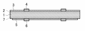
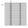
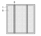
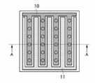
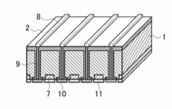
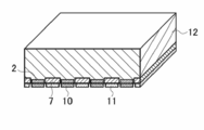
- FIG. 4 of the back contact type solar cell element It is a schematic sectional drawing which shows an example of the silicon type solar cell element concerning this invention. It is a schematic plan view which shows an example of the light-receiving surface of the silicon type solar cell element concerning this invention. It is a schematic plan view which shows an example of the back surface of the silicon type solar cell element concerning this invention. It is a schematic plan view which shows an example of the back surface side electrode structure of the back contact type solar cell element concerning this invention. It is a schematic perspective view which shows an example of AA cross-section structure in FIG. 4 of the back contact type solar cell element concerning this invention. It is a schematic perspective view which shows an example of AA cross-section structure in FIG. 4 of the back contact type solar cell element concerning this invention. It is a schematic perspective view which shows an example of AA cross-section structure in FIG. 4 of the back contact type solar cell element concerning this invention. It is a schematic perspective view which shows an example of AA cross-section structure in FIG. 4 of the back contact type solar cell element concerning
- the term “process” is not limited to an independent process, and is included in the term if the intended action of the process is achieved even when it cannot be clearly distinguished from other processes. .
- a numerical range indicated using “to” indicates a range including the numerical values described before and after “to” as the minimum value and the maximum value, respectively.
- the amount of each component in the composition in the present specification when there are a plurality of substances corresponding to each component in the composition, the plurality of the components present in the composition unless otherwise specified. It means the total amount of substance.
- the electrode paste composition of the present invention comprises at least one phosphorous-containing copper alloy particle, at least one tin-containing particle, at least one glass particle, at least one solvent, and at least one resin. Including. With such a configuration, oxidation of copper during firing in the atmosphere is suppressed, and an electrode with low resistivity can be formed. Furthermore, the formation of a reactant phase between copper and the silicon substrate is suppressed, and a good ohmic contact can be formed between the formed electrode and the silicon substrate.
- the electrode paste composition includes at least one type of phosphorus-containing copper alloy particles.
- a brazing material called phosphorus copper brazing (phosphorus concentration: about 7% by mass or less) is known.
- Phosphorus copper brazing is also used as a bonding agent between copper and copper, but by using phosphorus-containing copper alloy particles in the electrode paste composition of the present invention, the reductivity of phosphorus to copper oxide is utilized.
- an electrode having excellent oxidation resistance and low volume resistivity can be formed. Further, the electrode can be fired at a low temperature, and the effect that the process cost can be reduced can be obtained.
- the phosphorus content contained in the phosphorus-containing copper alloy in the present invention is preferably 6% by mass or more and 8% by mass or less from the viewpoint of oxidation resistance and low resistivity, and 6.3% by mass.
- the content is more preferably 7.8% by mass or less and more preferably 6.5% by mass or more and 7.5% by mass or less.
- the phosphorus-containing copper alloy particles are an alloy containing copper and phosphorus, but may further contain other atoms.
- other atoms include Ag, Mn, Sb, Si, K, Na, Li, Ba, Sr, Ca, Mg, Be, Zn, Pb, Cd, Tl, V, Sn, Al, Zr, W, Examples include Mo, Ti, Co, Ni, and Au.
- the content rate of the other atom contained in the said phosphorus containing copper alloy particle can be 3 mass% or less in the said phosphorus containing copper alloy particle, for example, from a viewpoint of oxidation resistance and a low resistivity, it is 1 It is preferable that it is below mass%.
- the phosphorus-containing copper alloy particles may be used singly or in combination of two or more.
- the particle diameter of the phosphorus-containing copper alloy particles is not particularly limited, but the particle diameter when the accumulated weight is 50% (hereinafter sometimes abbreviated as “D50%”) is 0.4 ⁇ m to 10 ⁇ m. It is preferably 1 ⁇ m to 7 ⁇ m. When the thickness is 0.4 ⁇ m or more, the oxidation resistance is more effectively improved. Moreover, the contact area with the phosphorus containing copper alloy particle
- the particle size of the phosphorus-containing copper alloy particles is measured by a microtrack particle size distribution measuring device (manufactured by Nikkiso Co., Ltd., MT3300 type).
- the shape of the phosphorus-containing copper alloy particles is not particularly limited, and may be any of a substantially spherical shape, a flat shape, a block shape, a plate shape, a scale shape, and the like, from the viewpoint of oxidation resistance and low resistivity. Therefore, it is preferably substantially spherical, flat, or plate-shaped.
- the content of the phosphorus-containing copper alloy particles in the electrode paste composition is not particularly limited. From the viewpoint of low resistivity, it is preferably 20% by mass to 85% by mass in the electrode paste composition, more preferably 25% by mass to 80% by mass, and more preferably 30% by mass to 75% by mass. More preferably, it is as follows.
- the phosphorus-containing copper alloy can be produced by a commonly used method.
- the phosphorus-containing copper alloy particles can be prepared using a normal method of preparing metal powder using a phosphorus-containing copper alloy prepared so as to have a desired phosphorus content, for example, a water atomization method Can be produced by a conventional method. For details of the water atomization method, the description of Metal Handbook (Maruzen Co., Ltd. Publishing Division) can be referred to.
- the desired phosphorus-containing copper alloy particles can be produced by dissolving the phosphorus-containing copper alloy, pulverizing this by nozzle spraying, and drying and classifying the obtained powder.
- grains which have a desired particle diameter can be manufactured by selecting classification conditions suitably.
- the electrode paste composition of the present invention contains at least one kind of tin-containing particles.
- tin-containing particles By including tin-containing particles in addition to phosphorus-containing copper alloy particles, an electrode having a low resistivity can be formed in the firing step described later.
- the phosphorus-containing copper alloy particles and the tin-containing particles react with each other in the firing step to form an electrode composed of a Cu—Sn alloy phase and a Sn—PO glass phase.
- the Cu—Sn alloy phase forms a dense bulk body in the electrode and functions as a conductive layer, thereby forming an electrode with low resistivity.
- the dense bulk body means that the massive Cu—Sn alloy phases are in close contact with each other to form a three-dimensional continuous structure.
- an electrode when an electrode is formed on a substrate containing silicon (hereinafter, also simply referred to as “silicon substrate”) using the electrode paste composition of the present invention, an electrode having high adhesion to the silicon substrate can be formed, Furthermore, good ohmic contact between the electrode and the silicon substrate can be achieved.
- This can be considered as follows, for example.
- the phosphorus-containing copper alloy particles and the tin-containing particles react with each other in the firing step to form an electrode composed of a Cu—Sn alloy phase and a Sn—PO glass phase. Since the Cu—Sn alloy phase is a dense bulk body, this Sn—PO glass phase is formed between the Cu—Sn alloy phase and the silicon substrate.
- Such an effect is generally manifested when an electrode is formed on a substrate containing silicon using the electrode paste composition of the present invention, and the type of substrate containing silicon is particularly limited. Is not to be done.
- substrate containing silicon the silicon substrate used for manufacture of the silicon substrate for solar cell formation, semiconductor devices other than a solar cell etc. can be mentioned, for example.
- the present invention by combining the phosphorus-containing copper alloy particles and the tin-containing particles in the electrode paste composition, first, by utilizing the reducibility of the phosphorus atoms in the phosphorus-containing copper alloy particles to the copper oxide, oxidation resistance An electrode having excellent properties and low volume resistivity is formed. Next, a reaction between the phosphorus-containing copper alloy particles and the tin-containing particles forms a conductive layer composed of a Cu—Sn alloy phase and a Sn—PO glass phase while keeping the volume resistivity low. And, for example, the Sn—PO glass phase functions as a barrier layer for preventing mutual diffusion of copper and silicon, thereby suppressing the formation of a reactant phase between the electrode and the silicon substrate. It can be considered that two characteristic mechanisms of forming a good ohmic contact with the electrode can be realized simultaneously in the firing step.
- the tin-containing particles are not particularly limited as long as they contain tin. Among them, at least one selected from tin particles and tin alloy particles is preferable, and at least one selected from tin alloy particles having a tin content of 1% by mass or more is preferable.
- the purity of tin in the tin particles is not particularly limited. For example, the purity of the tin particles can be 95% by mass or more, preferably 97% by mass or more, and preferably 99% by mass or more.
- the type of alloy is not particularly limited as long as the tin alloy particles are alloy particles containing tin.
- the tin alloy particles are alloy particles containing tin.
- it is preferably tin alloy particles having a tin content of 1% by mass or more, and the tin content is 3% by mass.
- the tin alloy particles are more preferably the above, more preferably tin alloy particles having a tin content of 5% by mass or more, and tin alloy particles having a tin content of 10% by mass or more. It is particularly preferred.
- tin alloy particles examples include Sn—Ag alloy, Sn—Cu alloy, Sn—Ag—Cu alloy, Sn—Ag—Sb alloy, Sn—Ag—Sb—Zn alloy, Sn—Ag— Cu—Zn alloy, Sn—Ag—Cu—Sb alloy, Sn—Ag—Bi alloy, Sn—Bi alloy, Sn—Ag—Cu—Bi alloy, Sn—Ag—In—Bi alloy, Sn—Sb alloy, Sn—Bi—Cu alloy, Sn—Bi—Cu—Zn alloy, Sn—Bi—Zn alloy, Sn—Bi—Sb—Zn alloy, Sn—Zn alloy, Sn— In-based alloys, Sn—Zn—In based alloys, Sn—Pb based alloys and the like can be mentioned.
- tin alloy particles in particular, Sn-3.5Ag, Sn-0.7Cu, Sn-3.2Ag-0.5Cu, Sn-4Ag-0.5Cu, Sn-2.5Ag-0.8Cu-0 .5Sb, Sn-2Ag-7.5Bi, Sn-3Ag-5Bi, Sn-58Bi, Sn-3.5Ag-3In-0.5Bi, Sn-3Bi-8Zn, Sn-9Zn, Sn-52In, Sn-40Pb
- Such tin alloy particles have the same or lower melting point as Sn (232 ° C.).
- these tin alloy particles can be suitably used in that they can melt at the initial stage of firing to cover the surface of the phosphorus-containing copper alloy particles and react uniformly with the phosphorus-containing copper alloy particles.
- the tin alloy particles include Sn-AX-BY-CZ, in which the element X contains A mass%, the element Y contains B mass%, and the element Z contains C mass%. Indicates that In the present invention, these tin-containing particles may be used alone or in combination of two or more.
- the tin-containing particles may further contain other atoms that are inevitably mixed.
- examples of other atoms inevitably mixed include Ag, Mn, Sb, Si, K, Na, Li, Ba, Sr, Ca, Mg, Be, Zn, Pb, Cd, Tl, V, Al, and Zr. , W, Mo, Ti, Co, Ni, Au, and the like.
- grain can be 3 mass% or less in the said tin containing particle
- the particle diameter of the tin-containing particles is not particularly limited, but the particle diameter when the accumulated weight is 50% (hereinafter sometimes abbreviated as “D50%”) is 0.5 ⁇ m to 20 ⁇ m. Is preferably 1 ⁇ m to 15 ⁇ m, more preferably 5 ⁇ m to 15 ⁇ m. When the thickness is 0.5 ⁇ m or more, the oxidation resistance of the tin-containing particles themselves is improved. Moreover, the contact area with the phosphorus containing copper alloy particle in an electrode becomes large because it is 20 micrometers or less, and reaction with phosphorus containing copper alloy particle advances effectively.
- the shape of the tin-containing particles is not particularly limited, and may be any of a substantially spherical shape, a flat shape, a block shape, a plate shape, a scale shape, and the like, from the viewpoint of oxidation resistance and low resistivity. It is preferably substantially spherical, flat, or plate-shaped.
- the content of tin-containing particles in the electrode paste composition of the present invention is not particularly limited. Especially, it is preferable that the content rate of the tin containing particle when the total content rate of the said phosphorus containing copper alloy particle and the said tin containing particle
- grain 5 mass% or more reaction with phosphorus containing copper alloy particle
- the tin-containing particles are 70% by mass or less, a sufficient volume of the Cu—Sn alloy phase can be formed, and the volume resistivity of the electrode is further reduced.
- the electrode paste composition of the present invention contains at least one kind of glass particles.
- the adhesion between the electrode portion and the substrate is improved during firing. Also.
- the silicon nitride film as the antireflection film is removed by so-called fire-through during firing, and an ohmic contact between the electrode and the silicon substrate is formed.
- the glass particles are glass particles containing glass having a glass softening point of 650 ° C. or lower and a crystallization start temperature exceeding 650 ° C. from the viewpoint of adhesion to the substrate and reduction in resistivity of the electrode. preferable.
- the glass softening point is measured by a usual method using a thermomechanical analyzer (TMA), and the crystallization start temperature is measured using a differential heat-thermogravimetric analyzer (TG-DTA). Measured by method.
- the glass particles are softened and melted at an electrode formation temperature to oxidize a contacted silicon nitride film, and oxidized silicon dioxide
- glass particles usually used in the technical field can be used without particular limitation.
- the glass particles contained in the electrode paste composition are composed of glass containing lead because silicon dioxide can be efficiently taken up.
- glass containing lead examples include those described in Japanese Patent No. 03050064, and these can also be suitably used in the present invention.
- lead-free glass that does not substantially contain lead in consideration of the influence on the environment.
- Examples of the lead-free glass include lead-free glass described in paragraph numbers 0024 to 0025 of JP-A-2006-313744 and lead-free glass described in JP-A-2009-188281. It is also preferable that the lead-free glass is appropriately selected and applied to the present invention.
- the glass softening point is 650 ° C. If it is the following and it is a glass particle containing the glass whose crystallization start temperature exceeds 650 degreeC, it can use without including a component required for fire through like the said lead.
- the glass component at least one selected from the group consisting of SiO 2 , P 2 O 5 , Al 2 O 3 , B 2 O 3 , V 2 O 5 , Bi 2 O 3 , ZnO, and PbO is used. It is preferable to use at least one selected from the group consisting of SiO 2 , PbO, B 2 O 3 , Bi 2 O 3 and Al 2 O 3 . In the case of such glass particles, the softening point is more effectively lowered. Furthermore, since the wettability with the phosphorus-containing copper alloy particles and the silver particles contained as necessary is improved, sintering between the particles proceeds in the firing process, and an electrode having a lower resistivity can be formed.
- glass particles containing phosphorous pentoxide (phosphate glass, P 2 O 5 glass particles) are preferable.
- diphosphorus pentoxide divanadium pentoxide is used.
- glass particles P 2 O 5 —V 2 O 5 glass particles.
- diphosphorus pentoxide-divanadium pentoxide glass particles P 2 O 5 —V 2 O 5 glass particles
- the content of divanadium pentoxide is 1% by mass or more based on the total mass of the glass. It is preferably 1% by mass to 70% by mass.
- the particle diameter of the glass particles in the present invention is not particularly limited, but the particle diameter (D50%) when the integrated weight is 50% is preferably 0.5 ⁇ m or more and 10 ⁇ m or less, and 0.8 ⁇ m or more. More preferably, it is 8 ⁇ m or less.
- the thickness is 0.5 ⁇ m or more, workability at the time of preparing the electrode paste composition is improved.
- it is 10 ⁇ m or less, it can be uniformly dispersed in the electrode paste composition, fire-through can be efficiently generated in the firing step, and adhesion to the silicon substrate is also improved.
- the shape of the glass particles is not particularly limited, and may be any of a substantially spherical shape, a flat shape, a block shape, a plate shape, a scale shape, and the like, from the viewpoint of oxidation resistance and low resistivity.
- a spherical shape, a flat shape, or a plate shape is preferable.
- the content of the glass particles is preferably 0.1% by mass to 10% by mass, more preferably 0.5% by mass to 8% by mass, based on the total mass of the electrode paste composition. More preferably, the content is 8% by mass to 8% by mass.
- the electrode paste composition of the present invention contains at least one solvent and at least one resin.
- the liquid physical property for example, a viscosity, surface tension, etc.
- the paste composition for electrodes of this invention can be adjusted to the required liquid physical property according to the provision method at the time of providing to a silicon substrate etc.
- the solvent is not particularly limited.
- hydrocarbon solvents such as hexane, cyclohexane and toluene
- chlorinated hydrocarbon solvents such as dichloroethylene, dichloroethane and dichlorobenzene
- cyclics such as tetrahydrofuran, furan, tetrahydropyran, pyran, dioxane, 1,3-dioxolane and trioxane Ether solvents
- amide solvents such as N, N-dimethylformamide and N, N-dimethylacetamide
- sulfoxide solvents such as dimethyl sulfoxide and diethyl sulfoxide
- ketone solvents such as acetone, methyl ethyl ketone, diethyl ketone and cyclohexanone
- ethanol Alcohol compounds such as 2-propanol, 1-butanol and diacetone alcohol; 2,2,4-trimethyl-1,3-pentane
- a polyhydric alcohol ester solvent, a terpene solvent, and a polyhydric alcohol ether solvent from the viewpoints of coatability and printability when the electrode paste composition is formed on a silicon substrate.
- a polyhydric alcohol ester solvent, a terpene solvent, and a polyhydric alcohol ether solvent from the viewpoints of coatability and printability when the electrode paste composition is formed on a silicon substrate.
- the solvents may be used singly or in combination of two or more.
- any resin that is usually used in the technical field can be used as long as it can be thermally decomposed by firing.
- cellulose resins such as methyl cellulose, ethyl cellulose, carboxymethyl cellulose, and nitrocellulose
- polyvinyl alcohols such as polyvinyl alcohols
- polyvinyl pyrrolidones acrylic resins
- vinyl acetate-acrylic acid ester copolymers such as polyvinyl butyral
- phenol examples thereof include alkyd resins such as modified alkyd resins and castor oil fatty acid modified alkyd resins; epoxy resins; phenol resins; rosin ester resins.
- the resin in the present invention is preferably at least one selected from a cellulose resin and an acrylic resin from the viewpoint of disappearance at the time of firing.
- the resins may be used alone or in combination of two or more.
- the weight average molecular weight of the resin in the present invention is not particularly limited.
- the weight average molecular weight is preferably from 5,000 to 500,000, and more preferably from 10,000 to 300,000. It can suppress that the viscosity of the paste composition for electrodes increases that the weight average molecular weight of the said resin is 5000 or more. This may be because, for example, the three-dimensional repulsion when adsorbed to phosphorus-containing copper alloy particles and tin-containing particles is insufficient, and the particles aggregate.
- the weight average molecular weight of the resin is 500000 or less, aggregation of the resins in the solvent is suppressed, and increase in the viscosity of the electrode paste composition can be suppressed.
- the weight average molecular weight of the resin is 500,000 or less, it is suppressed that the resin combustion temperature becomes high, and the resin is not completely burned when the electrode paste composition is fired, and remains as a foreign substance. Is suppressed, and the electrode can be configured to have a lower resistance.
- the content of the solvent and the resin can be appropriately selected according to the desired liquid properties and the type of solvent and resin used.
- the total content of the solvent and the resin is preferably 3% by mass or more and 29.9% by mass or less, and more preferably 5% by mass or more and 25% by mass or less, based on the total mass of the electrode paste composition. Preferably, it is 7 mass% or more and 20 mass% or less.
- the total content of phosphorus-containing copper alloy particles and tin-containing particles is 70% by mass or more and 94% by mass or less from the viewpoint of oxidation resistance and low resistivity of the electrode.
- the glass particle content is preferably 0.1% by mass or more and 10% by mass or less, and the total content of the solvent and the resin is preferably 3% by mass or more and 29.9% by mass or less.
- the phosphorus-containing copper alloy particles And the total content of tin-containing particles is 74% by mass or more and 88% by mass or less, the content of glass particles is 0.5% by mass or more and 8% by mass or less, and the total content of solvent and resin is 7%.
- the total content of the phosphorus-containing copper alloy particles and the tin-containing particles is 74% by mass or more and 88% by mass or less, and the glass particle content is 1% by mass or more. 8% by mass or less, solvent and resin It is more preferable that the total content of 20 mass% or less 7 mass% or more.
- the electrode paste composition of the present invention preferably further contains silver particles.
- silver particles By containing silver particles, the oxidation resistance is further improved, and the resistivity as an electrode is further reduced. Further, the Ag particles are precipitated in the Sn—PO system glass phase generated by the reaction between the phosphorus-containing copper alloy particles and the tin-containing particles, so that the Cu—Sn alloy phase and silicon in the electrode layer are deposited. The ohmic contact property between the substrates is further improved. Furthermore, the effect that the solder connection property at the time of setting it as a solar cell module improves is also acquired.
- the silver which comprises the said silver particle may contain the other atom mixed unavoidable.
- other atoms inevitably mixed for example, Sb, Si, K, Na, Li, Ba, Sr, Ca, Mg, Be, Zn, Pb, Cd, Tl, V, Sn, Al, Zr, W , Mo, Ti, Co, Ni, Au, and the like.
- the content rate of the other atom contained in the said silver particle can be 3 mass% or less in a silver particle, for example, and it is 1 mass% or less from a viewpoint of melting
- the particle diameter of the silver particles in the present invention is not particularly limited, but the particle diameter (D50%) when the accumulated weight is 50% is preferably 0.4 ⁇ m or more and 10 ⁇ m or less, and 1 ⁇ m or more and 7 ⁇ m or less. It is more preferable that When the thickness is 0.4 ⁇ m or more, the oxidation resistance is more effectively improved. Moreover, the contact area of the silver particle, phosphorus containing copper alloy particle
- the shape of the silver particles is not particularly limited, and may be any of a substantially spherical shape, a flat shape, a block shape, a plate shape, a scale shape, and the like, from the viewpoint of oxidation resistance and low resistivity.
- a spherical shape, a flat shape, or a plate shape is preferable.
- the content of silver particles is when the total content of the phosphorus-containing copper alloy particles, the tin-containing particles, and the silver particles is 100% by mass.
- the silver particle content is preferably 0.1% by mass or more and 10% by mass or less, and more preferably 0.5% by mass or more and 8% by mass or less.
- the electrode paste composition of the present invention comprises phosphorus-containing copper alloy particles, tin-containing particles, and The total content of silver particles is preferably 70% by mass or more and 94% by mass or less, and more preferably 74% by mass or more and 88% by mass or less.
- a suitable viscosity can be easily achieved when the electrode paste composition is applied.
- the total content of phosphorus-containing copper alloy particles, tin-containing particles and silver particles is 70 from the viewpoint of oxidation resistance and low resistivity of the electrode.
- the content of the glass particles is 0.1% by mass or more and 10% by mass or less, and the total content of the solvent and the resin is 3% by mass or more and 29.9% by mass or less.
- the total content of phosphorus-containing copper alloy particles, tin-containing particles and silver particles is 74% by mass to 88% by mass, and the glass particle content is 0.5% by mass to 8% by mass.
- the total content of the solvent and the resin is 7% by mass or more and 20% by mass or less, and the total content of the phosphorus-containing copper alloy particles, the tin-containing particles, and the silver particles is 74% by mass or more and 88% by mass. %, And the glass particle content is Be more than% by mass 8% by mass or less, it is more preferable that the total content of the solvent and the resin is 20 mass% or less 7 mass% or more.
- the electrode paste composition may further include at least one flux.
- the flux By including the flux, the oxide film formed on the surface of the phosphorus-containing copper alloy particles can be removed, and the reduction reaction of the phosphorus-containing copper alloy particles during firing can be promoted. Further, since the melting of the tin-containing particles during firing proceeds, the reaction with the phosphorus-containing copper alloy particles proceeds, and as a result, the oxidation resistance is further improved and the resistivity of the formed electrode is further decreased. Furthermore, the effect that the adhesiveness of an electrode material and a silicon substrate improves is also acquired.
- the flux in the present invention is not particularly limited as long as it can remove the oxide film formed on the surface of the phosphorus-containing copper alloy particles and promote the melting of the tin-containing particles.
- fatty acids, boric acid compounds, fluorinated compounds, borofluorinated compounds and the like can be mentioned as preferred fluxes.
- the flux includes lauric acid, myristic acid, palmitic acid, stearic acid, sorbic acid, stearic acid, propionic acid, boron oxide, potassium borate, sodium borate, lithium borate, potassium borofluoride, borofluoride.
- Sodium fluoride, lithium borofluoride, acidic potassium fluoride, acidic sodium fluoride, acidic lithium fluoride, potassium fluoride, sodium fluoride, lithium fluoride and the like can be mentioned.
- potassium borate and potassium borofluoride are particularly preferable fluxes from the viewpoints of heat resistance during electrode material firing (a property that the flux does not volatilize at low temperatures during firing) and supplementing oxidation resistance of the phosphorus-containing copper alloy particles.
- each of these fluxes may be used alone or in combination of two or more.
- the flux content is such that the oxidation resistance of the phosphorus-containing copper alloy particles is effectively expressed and the melting of the tin-containing particles is promoted and the electrode material
- the content is preferably 0.1% by mass to 5% by mass, and preferably 0.3% by mass to 4% by mass based on the total mass of the electrode paste composition. More preferably, it is 0.5% by mass to 3.5% by mass, particularly preferably 0.7% to 3% by mass, and 1% by mass to 2.5% by mass. It is very preferable that
- the electrode paste composition of the present invention can further contain other components that are usually used in the technical field, if necessary.
- other components include a plasticizer, a dispersant, a surfactant, an inorganic binder, a metal oxide, a ceramic, and an organometallic compound.
- the paste composition for electrodes of this invention there is no restriction
- the dispersion / mixing method is not particularly limited, and can be appropriately selected and applied from commonly used dispersion / mixing methods.
- the electrode paste composition is applied to a region where an electrode is to be formed, dried and then fired to form an electrode in a desired region. can do.
- an electrode having a low resistivity can be formed even when a baking treatment is performed in the presence of oxygen (for example, in the air).
- the electrode paste composition when a solar cell electrode is formed using the electrode paste composition, the electrode paste composition is applied on a silicon substrate so as to have a desired shape, and dried and fired. Thereby, a solar cell electrode with low resistivity can be formed in a desired shape. Further, by using the electrode paste composition, an electrode having a low resistivity can be formed even when a baking treatment is performed in the presence of oxygen (for example, in the air). Furthermore, the electrode formed on the silicon substrate has excellent adhesion to the silicon substrate, and can achieve a good ohmic contact.
- Examples of the method for applying the electrode paste composition include screen printing, an ink jet method, a dispenser method, and the like. From the viewpoint of productivity, application by screen printing is preferable.
- the electrode paste composition of the present invention When the electrode paste composition of the present invention is applied by screen printing, the electrode paste composition preferably has a viscosity in the range of 20 Pa ⁇ s to 1000 Pa ⁇ s. The viscosity of the electrode paste composition is measured at 25 ° C. using a Brookfield HBT viscometer.
- the application amount of the electrode paste composition can be appropriately selected according to the size of the electrode to be formed.
- the application amount of the electrode paste composition can be 2 g / m 2 to 10 g / m 2, and preferably 4 g / m 2 to 8 g / m 2 .
- heat treatment conditions when forming an electrode using the electrode paste composition of the present invention, heat treatment conditions usually used in the technical field can be applied.
- the heat treatment temperature is 800 ° C. to 900 ° C.
- heat treatment conditions at a lower temperature can be applied, for example, 450 ° C.
- An electrode having good characteristics can be formed at a heat treatment temperature of ⁇ 850 ° C.
- the heat treatment time can be appropriately selected according to the heat treatment temperature and the like, and can be, for example, 1 second to 20 seconds.
- any apparatus that can be heated to the above temperature can be used as appropriate, and examples thereof include an infrared heating furnace and a tunnel furnace.
- An infrared heating furnace is highly efficient because electric energy is directly input to a heating material in the form of electromagnetic waves and is converted into heat energy, and rapid heating is possible in a short time. Further, since there is no product due to combustion and non-contact heating, it is possible to suppress contamination of the generated electrode.
- the tunnel furnace automatically and continuously conveys the sample from the entrance to the exit and fires it, it can be fired uniformly by dividing the furnace body and controlling the transport speed. From the viewpoint of the power generation performance of the solar cell element, it is preferable to perform heat treatment with a tunnel furnace.
- the solar cell element of this invention has the electrode formed by baking the said paste composition for electrodes provided on the silicon substrate.
- the solar cell element which has a favorable characteristic is obtained, and it is excellent in productivity of this solar cell element.
- the solar cell element means one having a silicon substrate on which a pn junction is formed and an electrode formed on the silicon substrate.
- the solar cell is a state in which a tab wire is provided on the electrode of the solar cell element, and a plurality of solar cell elements are connected via the tab line as necessary and sealed with a sealing resin or the like. Means things.
- FIGS. 1 A sectional view showing an example of a typical solar cell element, and outlines of a light receiving surface and a back surface are shown in FIGS.
- single crystal or polycrystalline silicon is usually used for the semiconductor substrate 1 of the solar cell element.
- the semiconductor substrate 1 contains boron and constitutes a p-type semiconductor.
- irregularities also referred to as texture, not shown
- etching solution made of NaOH and IPA (isopropyl alcohol).
- the n + -type diffusion layer 2 is provided with a thickness of submicron order, and a pn junction is formed at the boundary with the p-type bulk portion. Further, on the light receiving surface side, an antireflection film 3 such as silicon nitride is provided on the n + type diffusion layer 2 with a film thickness of about 90 nm by PECVD or the like.
- the light-receiving surface electrode 4 and the back surface output extraction electrode 6 are formed from the electrode paste composition of the present invention.
- the back current collecting electrode 5 is formed of an aluminum electrode paste composition containing glass powder.
- the paste composition is applied to a desired pattern by screen printing or the like, then dried, and then in the atmosphere. It may be formed by firing at about 450 ° C. to 850 ° C. at the same time.
- an electrode having excellent resistivity and contact resistivity can be formed even when fired at a relatively low temperature.
- the glass particles contained in the electrode paste composition forming the light receiving surface electrode 4 react with the antireflection layer 3 (fire-through), and the light receiving surface electrode 4 and the n + The mold diffusion layer 2 is electrically connected (ohmic contact).
- the light-receiving surface electrode 4 is formed using the electrode paste composition, so that copper is suppressed as a conductive metal, and copper oxidation is suppressed. , Formed with good productivity.
- the formed electrode includes a Cu—Sn alloy phase and a Sn—PO glass phase, and the Sn—PO glass phase includes a Cu—Sn alloy phase and a silicon substrate. (Not shown) is more preferable. As a result, the reaction between copper and the silicon substrate is suppressed, and an electrode having low resistance and excellent adhesion can be formed.
- aluminum in the aluminum electrode paste composition that forms the back current collecting electrode 5 during firing diffuses to the back surface of the p-type silicon substrate 1 to form the p + -type diffusion layer 7.
- an ohmic contact can be obtained between the p-type silicon substrate 1, the back surface collecting electrode 5, and the back surface output extraction electrode 6.
- the aluminum electrode paste composition for forming the back surface collecting electrode 5 is first printed, and after drying, the atmosphere After baking at about 750 ° C. to 850 ° C. to form the back surface collecting electrode 5, the electrode paste composition of the present invention is printed on the light receiving surface side and back surface side, and after drying, 450 ° C. to 650 ° C. in the atmosphere.
- a method of forming the light-receiving surface electrode 4 and the back surface output extraction electrode 6 by firing at a degree is mentioned.
- This method is effective in the following cases, for example. That is, when the aluminum electrode paste forming the back surface collecting electrode 5 is fired, at a firing temperature of 650 ° C. or less, depending on the composition of the aluminum paste, the aluminum particles may be sintered and diffused into the p-type silicon substrate 1. In some cases, the amount of the p + -type diffusion layer cannot be sufficiently formed due to an insufficient amount. In this state, a sufficient ohmic contact cannot be formed between the p-type silicon substrate 1 on the back surface, the back surface collecting electrode 5 and the back surface output extraction electrode 6, and the power generation performance as a solar cell element may be reduced. Therefore, after forming the back current collecting electrode 5 at an optimum firing temperature (for example, 750 ° C.
- the electrode paste composition of the present invention is printed and dried at a relatively low temperature (
- the light-receiving surface electrode 4 and the back surface output extraction electrode 6 are formed by baking at 450 ° C. to 650 ° C.
- FIG. 4 is a schematic plan view of a back-side electrode structure common to a so-called back contact solar cell element according to another embodiment of the present invention, and FIG. 4 shows an outline of a solar cell element which is a back contact solar cell element according to another embodiment.
- the perspective view which shows a structure is shown in FIG.5, FIG6 and FIG.7, respectively. 5, 6, and 7 are perspective views taken along a section AA in FIG. 4.
- the p-type silicon substrate 1 is formed with through holes penetrating both the light receiving surface side and the back surface side by laser drilling or etching. Further, a texture (not shown) for improving the light incident efficiency is formed on the light receiving surface side. Further, on the light receiving surface side, an n + -type diffusion layer 2 by n-type diffusion treatment and an antireflection film (not shown) are formed on the n + -type diffusion layer 2. These are manufactured by the same process as a conventional crystalline Si type solar cell element.
- the electrode paste composition of the present invention is filled into the previously formed through-holes by a printing method or an ink jet method, and the electrode paste composition of the present invention is also formed in a grid on the light receiving surface side.
- the composition layer which is printed and forms the through-hole electrode 9 and the light receiving surface collecting electrode 8 is formed.
- an n + -type diffusion layer 2 and a p + -type diffusion layer 7 for preventing carrier recombination are formed on the back surface side.
- boron (B) or aluminum (Al) is used as an impurity element for forming the p + -type diffusion layer 7.
- the p + -type diffusion layer 7 may be formed, for example, by performing a thermal diffusion process using B as a diffusion source in the solar cell element manufacturing process before the formation of the antireflection film, or by using Al. When using, in the said printing process, you may form by printing and baking an aluminum paste on the opposite surface side.
- the electrode paste composition of the present invention is printed on the n + -type diffusion layer 2 and the p + -type diffusion layer 7 in stripes, thereby forming the back electrode. 10 and 11 are formed.
- the back electrode may be formed using the electrode paste composition of the present invention only on the n + type diffusion layer 2 side.
- the solar cell element having the structure shown in the perspective view of FIG. 6 can be manufactured in the same manner as the solar cell element having the structure shown in the perspective view of FIG. 5 except that the light receiving surface collecting electrode is not formed. it can. That is, in the solar cell element having the structure shown in the perspective view of FIG. 6, the electrode paste composition of the present invention can be used for the through-hole electrode 9 and the back electrodes 10 and 11.
- the solar cell element having the structure shown in the perspective view of FIG. 7 has the structure shown in the perspective view of FIG. 5 except that the n-type silicon substrate 12 is used as a base substrate and no through hole is formed. It can be manufactured in the same manner as a solar cell element having That is, in the solar cell element having the structure shown in the perspective view of FIG. 7, the electrode paste composition of the present invention can be used for the back electrodes 10 and 11.
- the electrode paste composition of the present invention is not limited to the use of the solar cell electrode as described above.
- electrode wiring and shield wiring of a plasma display, ceramic capacitor, antenna circuit, various sensor circuits It can also be suitably used for applications such as heat dissipation materials for semiconductor devices. Among these, it can be suitably used particularly when an electrode is formed on a substrate containing silicon.
- the solar cell of the present invention includes at least one of the solar cell elements, and is configured by arranging tab wires on the electrodes of the solar cell element. If necessary, the solar cell may be configured by connecting a plurality of solar cell elements via tab wires and further sealing with a sealing material.
- the tab wire and the sealing material are not particularly limited, and can be appropriately selected from those usually used in the art.
- Example 1> Preparation of electrode paste composition
- Phosphorus-containing copper alloy particles containing 7% by mass of phosphorus were prepared by a conventional method, dissolved and powdered by a water atomization method, and then dried and classified. The classified powders were blended and subjected to deoxygenation / dehydration treatment to produce phosphorus-containing copper alloy particles containing 7% by mass of phosphorus.
- the phosphorus-containing copper alloy particles had a particle size (D50%) of 5.0 ⁇ m and a substantially spherical shape.
- a glass composed of 9 parts of zinc oxide (ZnO) (hereinafter sometimes abbreviated as “G01”) was prepared.
- the obtained glass G01 had a softening point of 420 ° C. and a crystallization temperature of over 650 ° C.
- glass G01 particles having a particle diameter (D50%) of 2.5 ⁇ m were obtained.
- the shape was substantially spherical.
- FIG. 1 A p-type semiconductor substrate having a thickness of 190 ⁇ m having an n + -type diffusion layer, a texture, and an antireflection film (silicon nitride film) formed on the light receiving surface is prepared, and the size is 125 mm ⁇ 125 mm. Cut out.
- the electrode paste composition 1 obtained above was printed so as to have an electrode pattern as shown in FIG.
- the electrode pattern was composed of a finger line with a width of 150 ⁇ m and a bus bar with a width of 1.5 mm, and the printing conditions (screen plate mesh, printing speed, printing pressure) were appropriately adjusted so that the film thickness after firing was 20 ⁇ m. This was placed in an oven heated to 150 ° C. for 15 minutes, and the solvent was removed by evaporation.
- the electrode paste composition 1 and the aluminum electrode paste were printed by screen printing in the same manner as described above so as to have an electrode pattern as shown in FIG.
- the pattern of the back surface output extraction electrode made of the electrode paste composition 1 was 123 mm ⁇ 5 mm, and was printed in two places in total.
- the printing conditions (screen plate mesh, printing speed, printing pressure) were appropriately adjusted so that the back surface output extraction electrode had a film thickness after firing of 20 ⁇ m.
- an aluminum electrode paste was printed on the entire surface other than the back surface output extraction electrode to form a back surface current collecting electrode pattern.
- the printing conditions of the aluminum electrode paste were appropriately adjusted so that the film thickness of the back surface collecting electrode after firing was 30 ⁇ m. This was placed in an oven heated to 150 ° C. for 15 minutes, and the solvent was removed by evaporation.
- a heat treatment (firing) is performed at a firing maximum temperature of 800 ° C. and a holding time of 10 seconds in an air atmosphere to form a desired electrode.
- the produced solar cell element 1 was produced.
- Example 2 a solar cell element 2 was produced in the same manner as in Example 1 except that the firing condition at the time of electrode formation was changed from a maximum temperature of 800 ° C. for 10 seconds to a maximum temperature of 850 ° C. for 8 seconds.
- Example 3 In Example 1, except that the phosphorus content of the phosphorus-containing copper alloy particles was changed from 7% by mass to 6% by mass, an electrode paste composition 3 was prepared in the same manner as in Example 1, and the solar cell element 3 was produced.
- Example 4 a solar cell element 4 was produced in the same manner as in Example 3 except that the firing condition at the time of electrode formation was changed from 10 seconds at a maximum temperature of 800 ° C. to 12 seconds at a maximum temperature of 750 ° C.
- Example 5 In Example 1, except that the phosphorus content of the phosphorus-containing copper alloy particles was changed from 7% by mass to 8% by mass, an electrode paste composition 5 was prepared in the same manner as in Example 1, and the solar cell element 5 was produced.
- Example 6> In Example 1, except that the particle size (D50%) of the phosphorus-containing copper alloy particles was changed from 5.0 ⁇ m to 1.5 ⁇ m, the electrode paste composition 6 was prepared in the same manner as in Example 1, A solar cell element 6 was produced.
- Example 7 In Example 1, the contents of phosphorus-containing copper alloy particles and tin-containing particles were changed so that the content of phosphorus-containing copper alloy particles was 56.3 parts and the content of tin-containing particles was 25.1 parts. Except for this, a paste composition for electrode 7 was prepared in the same manner as in Example 1, and a solar cell element 7 was produced.
- Example 8 In Example 1, the contents of the phosphorus-containing copper alloy particles and tin-containing particles were changed so that the content of the phosphorus-containing copper alloy particles was 73.0 parts and the content of the tin-containing particles was 8.4 parts. Except for this, in the same manner as in Example 1, an electrode paste composition 8 was prepared, and a solar cell element 8 was produced.
- Example 9 In Example 1, instead of tin particles (Sn), tin alloy particles made of Sn-58Bi (an alloy containing 58 mass% Bi in Sn) were used as the tin-containing particles, and the particle diameter (D50%) was 15. Except having set to 0 micrometer, it carried out similarly to Example 1, the electrode paste composition 9 was prepared, and the solar cell element 9 was produced.
- Sn tin particles
- Sn-58Bi an alloy containing 58 mass% Bi in Sn
- Example 10 tin alloy particles made of Sn-4Ag-0.5Cu (an alloy containing 4 mass% of Ag and 0.5 mass% of Cu in Sn) instead of tin particles (Sn) were used as tin-containing particles.
- An electrode paste composition 10 was prepared in the same manner as in Example 1 except that the particle diameter (D50%) was 8.0 ⁇ m, and a solar cell element 10 was produced.
- Example 11 In Example 1, except that the particle diameter (D50%) of the tin-containing particles was changed from 10.0 ⁇ m to 6.0 ⁇ m, the electrode paste composition 11 was prepared in the same manner as in Example 1, and the solar cell Element 11 was produced.
- Example 12 In Example 1, silver particles (Ag; particle diameter (D50%) 3.0 ⁇ m; purity 99.5%) were added to the electrode paste composition. Specifically, the content of each component is 37.9 parts of phosphorus-containing copper alloy particles, 39.5 parts of tin particles, 4.0 parts of silver particles, 4.1 parts of glass G01 particles, and 14 parts of terpineol. Except having changed 0.1 part and ethyl cellulose into 0.4 part, it carried out similarly to Example 1, the paste composition 12 for electrodes was prepared, and the solar cell element 12 was produced.
- Example 13 In Example 1, silver particles (Ag; particle size (D50%) 3.0 ⁇ m) were further added to the electrode paste composition. Specifically, the content of each component is 36.9 parts of phosphorus-containing copper alloy particles, 38.4 parts of tin particles, 6.1 parts of silver particles, 4.1 parts of glass G01 particles, and 14 parts of terpineol. Except having changed 0.1 part and ethyl cellulose into 0.4 part, it carried out similarly to Example 1, the paste composition 13 for electrodes was prepared, and the solar cell element 13 was produced.
- Example 14 In Example 1, the content of the glass G01 particles was changed. Specifically, the content of each component is 38.3 parts of phosphorus-containing copper alloy particles, 39.9 parts of tin particles, 7.8 parts of glass G01 particles, 13.5 parts of terpineol, and 0.03 of ethyl cellulose. Except having changed into 4 parts, it carried out similarly to Example 1, and prepared the paste composition 14 for electrodes, and produced the solar cell element 14.
- FIG. 1 the content of the glass G01 particles was changed. Specifically, the content of each component is 38.3 parts of phosphorus-containing copper alloy particles, 39.9 parts of tin particles, 7.8 parts of glass G01 particles, 13.5 parts of terpineol, and 0.03 of ethyl cellulose. Except having changed into 4 parts, it carried out similarly to Example 1, and prepared the paste composition 14 for electrodes, and produced the solar cell element 14.
- FIG. 1 the content of the glass G01 particles was changed. Specifically, the content of each component is 38.3 parts of
- Example 15 In Example 1, except that the composition of the glass particles was changed from the glass G01 to the glass G02 shown below, an electrode paste composition 15 was prepared in the same manner as in Example 1 to produce the solar cell element 15. did.
- Glass G02 is composed of 45 parts of vanadium oxide (V 2 O 5 ), 24.2 parts of phosphorus oxide (P 2 O 5 ), 20.8 parts of barium oxide (BaO), 5 parts of antimony oxide (Sb 2 O 3 ), oxidation It was prepared to consist of 5 parts of tungsten (WO 3 ). Further, the softening point of the glass G02 was 492 ° C., and the crystallization start temperature exceeded 650 ° C.
- glass G02 particles having a particle diameter (D50%) of 2.5 ⁇ m were obtained. The shape was substantially spherical.
- Example 16 In Example 1, the resin was changed from terpineol to diethylene glycol monobutyl ether (BC), and the resin was changed from ethyl cellulose to polyethyl acrylate (EPA). Specifically, the content of each component is 39.9 parts of phosphorus-containing copper alloy particles, 41.5 parts of tin particles, 4.1 parts of glass G01 particles, 12.3 parts of diethylene glycol monobutyl ether, polyacrylic Except having changed ethyl acid into 2.2 parts, it carried out similarly to Example 1, the electrode paste composition 16 was prepared, and the solar cell element 16 was produced.
- BC terpineol to diethylene glycol monobutyl ether
- EPA polyethyl acrylate
- Example 17 phosphorus content of phosphorus-containing copper alloy particles, particle diameter (D50%) and its content, composition of tin-containing particles, particle diameter (D50%) and its content, silver particle content, glass
- the paste composition 17 for an electrode was the same as in Example 1 except that the type and content of particles, the type and content of solvent, the type and content of resin were changed as shown in Table 1.
- ⁇ 20 were prepared respectively.
- a desired electrode was formed in the same manner as in Example 1 except that the obtained electrode paste compositions 17 to 20 were used, respectively, and the heat treatment temperature and treatment time were changed as shown in Table 1.
- the solar cell elements 17 to 20 thus prepared were respectively produced.
- Example 21 A p-type semiconductor substrate having a film thickness of 190 ⁇ m having an n + -type diffusion layer, a texture, and an antireflection film (silicon nitride film) formed on the light receiving surface was prepared and cut into a size of 125 mm ⁇ 125 mm. Thereafter, an aluminum electrode paste was printed on the back surface to form a back surface collecting electrode pattern. The back surface collecting electrode pattern was printed on the entire surface other than the back surface output extraction electrode as shown in FIG. Moreover, the printing conditions of the aluminum electrode paste were appropriately adjusted so that the film thickness of the back surface collecting electrode after firing was 30 ⁇ m. This was placed in an oven heated to 150 ° C. for 15 minutes, and the solvent was removed by evaporation.
- the electrode paste composition 1 obtained above was printed so as to have an electrode pattern as shown in FIGS.
- the electrode pattern on the light-receiving surface is composed of 150 ⁇ m wide finger lines and 1.5 mm wide bus bars, and printing conditions (screen plate mesh, printing speed, printing pressure) are appropriately set so that the film thickness after firing is 20 ⁇ m. It was adjusted.
- the back electrode pattern was 123 mm ⁇ 5 mm, and was printed in two places so that the film thickness after firing was 20 ⁇ m. This was placed in an oven heated to 150 ° C. for 15 minutes, and the solvent was removed by evaporation.
- Example 22 a solar cell element 22 was produced in the same manner as in Example 21, except that the electrode paste composition 5 obtained above was used to produce the light receiving surface electrode and the back surface output extraction electrode.
- Example 23 In Example 21, the electrode paste composition 9 obtained above was used for the production of the light receiving surface electrode and the back surface output extraction electrode, and the firing conditions during electrode formation were 10 seconds at the maximum temperature of 650 ° C. A solar cell element 23 was produced in the same manner as in Example 21 except that the maximum temperature was changed to 620 ° C. for 10 seconds.
- a solar cell element 24 having a structure as shown in FIG. 5 was produced.
- a specific manufacturing method is described below.
- the previously formed through-hole internal electrode paste composition 1 was filled by an inkjet method, and further printed on the light-receiving surface side in a grid.
- the electrode paste composition 1 and the aluminum electrode paste were used to print in stripes in a pattern as shown in FIG. 4, and the electrode paste composition 1 was printed under the through holes. Formed as follows. This was subjected to heat treatment using a tunnel furnace (manufactured by Noritake Co., Ltd., single-row transport W / B tunnel furnace) in an air atmosphere at a firing maximum temperature of 800 ° C. for a holding time of 10 seconds, and the sun on which the desired electrode was formed A battery element 24 was produced. At this time, with respect to the part where the aluminum electrode paste was formed, Al diffused into the p-type silicon substrate by firing, whereby a p + -type diffusion layer was formed.
- a tunnel furnace manufactured by Noritake Co., Ltd., single-row transport W / B tunnel furnace
- Example 25 In Example 24, except that the electrode paste composition 1 was changed from the electrode paste composition 1 to the electrode paste composition 12 obtained above, the light receiving surface current collecting electrode, the through-hole electrode, and the back surface electrode were formed. In the same manner as in Example 24, a solar cell element 25 was produced.
- Example 26 a solar cell element 26 was produced in the same manner as in Example 24, except that the firing condition at the time of electrode formation was changed from a maximum temperature of 800 ° C. for 10 seconds to a maximum temperature of 850 ° C. for 8 seconds.
- Example 27 In Example 24, except that the electrode paste composition 1 was changed to the electrode paste composition 9 obtained above to form a light-receiving surface collecting electrode, a through-hole electrode, and a back electrode, the Example In the same manner as in Example 24, a solar cell element 27 was produced.
- Example 28 In Example 1, an electrode paste composition 28 was prepared in the same manner as in Example 1 except that the glass particles were changed from glass G01 particles to glass G03 particles.
- Glass G03 is composed of 13 parts of silicon dioxide (SiO 2 ), 58 parts of boron oxide (B 2 O 3 ), 38 parts of zinc oxide (ZnO), 12 parts of aluminum oxide (Al 2 O 3 ), and barium oxide (BaO). Prepared to consist of 12 parts.
- the obtained glass G03 had a softening point of 583 ° C. and a crystallization temperature of over 650 ° C.
- glass G03 particles having a particle diameter (D50%) of 2.5 ⁇ m were obtained. The shape was substantially spherical.
- a solar cell element 28 having a structure as shown in FIG. 6 was produced using the electrode paste composition 28 obtained above.
- the manufacturing method is the same as in Examples 24 to 27 except that the light receiving surface electrode is not formed.
- the firing conditions were a maximum temperature of 800 ° C. and a holding time of 10 seconds.
- Example 29 a solar cell element 29 was produced in the same manner as in Example 28, except that the firing condition at the time of electrode formation was changed from a maximum temperature of 800 ° C. for 10 seconds to a maximum temperature of 850 ° C. for 8 seconds.
- Example 30 Using the electrode paste composition 28 obtained above, a solar cell element 30 having a structure as shown in FIG. 7 was produced.
- the manufacturing method is the same as that in Example 24 except that an n-type silicon substrate was used as the base substrate and that the light-receiving surface electrode, the through hole, and the through hole electrode were not formed.
- the firing conditions were a maximum temperature of 800 ° C. and a holding time of 10 seconds.
- Example 31 In Example 5, electrode paste composition 31 was prepared in the same manner as in Example 5 except that the glass particles were changed from glass G01 particles to glass G03 particles. Using this, a solar cell element 31 having a structure as shown in FIG.
- Example 32 an electrode paste composition 32 was prepared in the same manner as in Example 12 except that the glass particles were changed from glass G01 particles to glass G03 particles. Using this, a solar cell element 32 having a structure as shown in FIG.
- Example 1 In the preparation of the electrode paste composition in Example 1, Example 1 was used except that each component was changed to the composition shown in Table 1 without using phosphorus-containing copper alloy particles and tin-containing particles. Similarly, electrode paste composition C1 was prepared. A solar cell element C1 was produced in the same manner as in Example 1 except that the electrode paste composition C1 not containing phosphorus-containing copper alloy particles and tin-containing particles was used.
- Electrode paste compositions C2 to C4 having the compositions shown in Table 1 were prepared.
- Solar cell elements C2 to C4 were respectively produced in the same manner as in Comparative Example 1 except that the electrode paste compositions C2 to C4 were used.
- Example 5 In the preparation of the electrode paste composition in Example 1, copper particles (purity 99.5%, particle diameter (D50%) 5.0 ⁇ m, content 39.9 parts) were used instead of phosphorus-containing copper alloy particles.
- An electrode paste composition C5 was prepared in the same manner as in Example 1 except that each component was changed to have the composition shown in Table 1.
- a solar cell element C5 was produced in the same manner as in Comparative Example 1 except that the electrode paste composition C5 was used.
- Example 24 In Example 24, except that the electrode paste composition C1 was changed from the electrode paste composition 1 to the electrode paste composition C1 obtained above, the light receiving surface collecting electrode, the through-hole electrode, and the back electrode were formed. In the same manner as in Example 24, a solar cell element C6 was produced.
- Example 28 a solar cell element C7 was produced in the same manner as in Example 28 except that the electrode paste composition 28 was changed to the electrode paste composition C1 obtained above.
- Example 30 a solar cell element C8 was produced in the same manner as in Example 30, except that the electrode paste composition 28 was changed to the electrode paste composition C1 obtained above.
- the obtained measured values are converted into relative values with the measured value of Comparative Example 1 (solar cell element C1) as 100.0, and are shown in Table 2.
- Comparative Example 2 the resistivity of the electrode increased due to oxidation of the copper particles, and evaluation was impossible.
- the cross section of the light-receiving surface electrode formed by firing the prepared electrode paste composition was observed with a scanning electron microscope Miniscope TM-1000 (manufactured by Hitachi, Ltd.) at an acceleration voltage of 15 kV.
- the presence or absence of the Cu—Sn alloy phase, Sn—PO glass phase, and the formation site of the Sn—PO glass phase were investigated. The results are also shown in Table 2.
- Comparative Examples 3 to 5 the power generation performance deteriorated as compared with Comparative Example 1. This is considered as follows, for example.
- Comparative Example 4 since tin-containing particles are not included, it is considered that interdiffusion between the silicon substrate and copper occurred during firing, and the pn junction characteristics in the substrate deteriorated.
- pure copper phosphorus content 0 mass%) was used without using the phosphorus-containing copper alloy particles, so that the copper particles were oxidized before reacting with the tin-containing particles during firing, and Cu— It is conceivable that the resistance of the electrode was increased without forming the Sn alloy phase.
- the power generation performance of the solar cell elements produced in Examples 1 to 23 was almost the same as the measured value of the solar cell element of Comparative Example 1.
- the solar cell elements 21 to 23 exhibited high power generation performance even though the electrode paste composition was fired at a relatively low temperature (620 to 650 ° C.).
- a Cu—Sn alloy phase and a Sn—PO glass phase are present in the light receiving surface electrode, and a Sn—PO glass phase is formed between the Cu—Sn alloy phase and the silicon substrate. It had been.
- the solar cell elements produced in Examples 30 to 32 exhibited almost the same power generation performance as the solar cell element of Comparative Example 8. Further, as a result of the structure observation, the Cu—Sn alloy phase and the Sn—PO glass phase exist in the electrode formed by firing the prepared electrode paste composition among the back electrodes, and Sn—PO A glass phase was formed between the Cu—Sn alloy phase and the silicon substrate.
Landscapes
- Engineering & Computer Science (AREA)
- Physics & Mathematics (AREA)
- Computer Hardware Design (AREA)
- Condensed Matter Physics & Semiconductors (AREA)
- General Physics & Mathematics (AREA)
- Microelectronics & Electronic Packaging (AREA)
- Power Engineering (AREA)
- Sustainable Development (AREA)
- Life Sciences & Earth Sciences (AREA)
- Sustainable Energy (AREA)
- Electromagnetism (AREA)
- Chemical & Material Sciences (AREA)
- Dispersion Chemistry (AREA)
- Spectroscopy & Molecular Physics (AREA)
- Manufacturing & Machinery (AREA)
- Crystallography & Structural Chemistry (AREA)
- Conductive Materials (AREA)
- Photovoltaic Devices (AREA)
- Internal Circuitry In Semiconductor Integrated Circuit Devices (AREA)
Abstract
Description
また前記錫含有粒子は、錫粒子及び錫含有率が1質量%以上である錫合金粒子から選ばれる少なくとも1種類であることが好ましい。
本発明の電極用ペースト組成物は、リン含有銅合金粒子の少なくとも1種と、錫含有粒子の少なくとも1種と、ガラス粒子の少なくとも1種と、溶剤の少なくとも1種と、樹脂の少なくとも1種とを含む。かかる構成であることにより、大気中焼成時における銅の酸化が抑制され、抵抗率の低い電極を形成できる。さらに銅とシリコン基板との反応物相の形成が抑制され、形成される電極とシリコン基板とが良好なオーミックコンタクトを形成できる。
電極ペースト組成物は、リン含有銅合金粒子の少なくとも1種を含む。リン含有銅合金としては、リン銅ろう(リン濃度:7質量%程度以下)と呼ばれるろう付け材料が知られている。リン銅ろうは、銅と銅との接合剤としても用いられるものであるが、本発明の電極用ペースト組成物にリン含有銅合金粒子を用いることで、リンの銅酸化物に対する還元性を利用し、耐酸化性に優れ、体積抵抗率の低い電極を形成することができる。さらに電極の低温焼成が可能となり、プロセスコストを削減できるという効果を得ることができる。
また前記リン含有銅合金粒子に含まれる他の原子の含有率は、例えば、前記リン含有銅合金粒子中に3質量%以下とすることができ、耐酸化性と低抵抗率の観点から、1質量%以下であることが好ましい。
また前記リン含有銅合金粒子の形状としては特に制限はなく、略球状、扁平状、ブロック状、板状、及び鱗片状等のいずれであってもよいが、耐酸化性と低抵抗率の観点から、略球状、扁平状、または板状であることが好ましい。
具体的には、リン含有銅合金を溶解し、これをノズル噴霧によって粉末化した後、得られた粉末を乾燥、分級することで、所望のリン含有銅合金粒子を製造することができる。また、分級条件を適宜選択することで所望の粒子径を有するリン含有銅合金粒子を製造することができる
本発明の電極用ペースト組成物は、錫含有粒子の少なくとも1種を含む。リン含有銅合金粒子に加えて、錫含有粒子を含むことにより、後述する焼成工程において、抵抗率の低い電極を形成できる。
これは例えば以下のように考えることができる。リン含有銅合金粒子と錫含有粒子とが、焼成工程で互いに反応して、Cu-Sn合金相とSn-P-Oガラス相からなる電極を形成する。ここで前記Cu-Sn合金相は、電極内で緻密なバルク体を形成し、これが導電層として機能することで抵抗率の低い電極を形成できると考えられる。
尚、ここでいう緻密なバルク体とは、塊状のCu-Sn合金相が互いに密に接触し、三次元的に連続している構造を形成していることを意味する。
これは例えば以下のように考えることができる。リン含有銅合金粒子と錫含有粒子とが、焼成工程で互いに反応して、Cu-Sn合金相とSn-P-Oガラス相からなる電極を形成する。上記Cu-Sn合金相が緻密なバルク体であるために、このSn-P-Oガラス相は、Cu-Sn合金相とシリコン基板との間に形成される。これによりCu-Sn合金相のシリコン基板に対する密着性が向上すると考えることができる。またSn-P-Oガラス相が、銅とシリコンとの相互拡散を防止するためのバリア層として機能することで、焼成して形成される電極とシリコン基板との良好なオーミックコンタクトが達成できると考えることができる。すなわち銅を含む電極とシリコンを直に接触して加熱したときに形成される反応相(Cu3Si)の形成を抑制し、半導体性能(例えば、pn接合特性)を劣化することなくシリコン基板との密着性を保ちながら、良好なオーミックコンタクトを発現することができると考えられる。
錫粒子における錫の純度は特に制限されない。例えば錫粒子の純度は、95質量%以上とすることができ、97質量%以上であることが好ましく、99質量%以上であることが好ましい。
本発明において、これらの錫含有粒子は1種単独で使用してもよく、又2種類以上を組み合わせて使用することもできる。
また前記錫含有粒子に含まれる他の原子の含有率は、例えば前記錫含有粒子中に3質量%以下とすることができ、融点及びリン含有銅合金粒子との反応性の観点から、1質量%以下であることが好ましい。
また前記錫含有粒子の形状としては特に制限はなく、略球状、扁平状、ブロック状、板状、及び鱗片状等のいずれであってもよいが、耐酸化性と低抵抗率の観点から、略球状、扁平状、または板状であることが好ましい。
錫含有粒子の含有率を5質量%以上とすることで、リン含有銅合金粒子との反応をより均一に生じさせることができる。また錫含有粒子を70質量%以下とすることで、充分な体積のCu-Sn合金相を形成することができ、電極の体積抵抗率がより低下する。
本発明の電極用ペースト組成物は、ガラス粒子の少なくとも1種を含む。電極用ペースト組成物がガラス粒子を含むことにより、焼成時に電極部と基板との密着性が向上する。また。特に太陽電池受光面側の電極形成において、焼成時にいわゆるファイアースルーによって反射防止膜である窒化ケイ素膜が取り除かれ、電極とシリコン基板とのオーミックコンタクトが形成される。
また本発明においては、環境に対する影響を考慮すると、鉛を実質的に含まない鉛フリーガラスを用いることが好ましい。鉛フリーガラスとしては、例えば、特開2006-313744号公報の段落番号0024~0025に記載の鉛フリーガラスや、特開2009-188281号公報等に記載の鉛フリーガラスを挙げることができ、これらの鉛フリーガラスから適宜選択して本発明に適用することもまた好ましい。
また前記ガラス粒子の形状としては特に制限はなく、略球状、扁平状、ブロック状、板状、及び鱗片状等のいずれであってもよいが、耐酸化性と低抵抗率の観点から、略球状、扁平状、または板状であることが好ましい。
本発明の電極用ペースト組成物は、溶剤の少なくとも1種と樹脂の少なくとも1種とを含む。これにより本発明の電極用ペースト組成物の液物性(例えば、粘度、表面張力等)を、シリコン基板等に付与する際の付与方法に応じて必要とされる液物性に調整することができる。
また本発明において前記溶剤は1種単独でも、2種以上を組み合わせて用いてもよい。
また本発明において前記樹脂は1種単独でも、2種以上を組み合わせて用いてもよい。
またこれに加え樹脂の重量平均分子量が500000以下であると、樹脂の燃焼温度が高くなることが抑制され、電極用ペースト組成物を焼成する際に樹脂が完全に燃焼されず異物として残存することが抑制され、電極をより低抵抗に構成することができる。
溶剤と樹脂の総含有率が前記範囲内であることにより、電極用ペースト組成物をシリコン基板に付与する際の付与適性が良好になり、所望の幅及び高さを有する電極をより容易に形成することができる。
本発明の電極用ペースト組成物は、銀粒子を更に含むことが好ましい。銀粒子を含むことで耐酸化性がより向上し、電極としての抵抗率がより低下する。また、前記リン含有銅合金粒子と前記錫含有粒子との反応によって生成したSn-P-O系ガラス相の中にAg粒子が析出することで、電極層の中のCu-Sn合金相とシリコン基板間のオーミックコンタクト性がより向上する。さらに太陽電池モジュールとした場合のはんだ接続性が向上するという効果も得られる。
また前記銀粒子に含まれる他の原子の含有率は、例えば銀粒子中に3質量%以下とすることができ、融点及び電極の低抵抗率化の観点から、1質量%以下であることが好ましい。
また前記銀粒子の形状としては特に制限はなく、略球状、扁平状、ブロック状、板状、及び鱗片状等のいずれであってもよいが、耐酸化性と低抵抗率の観点から、略球状、扁平状、または板状であることが好ましい。
電極用ペースト組成物は、フラックスの少なくとも1種をさらに含むことができる。フラックスを含むことでリン含有銅合金粒子の表面に形成された酸化膜を除去し、焼成中のリン含有銅合金粒子の還元反応を促進させることができる。また焼成中の錫含有粒子の溶融も進むためリン含有銅合金粒子との反応が進み、結果として耐酸化性がより向上し、形成される電極の抵抗率がより低下する。さらに電極材とシリコン基板の密着性が向上するという効果も得られる。
中でも、電極材焼成時の耐熱性(フラックスが焼成の低温時に揮発しない特性)及びリン含有銅合金粒子の耐酸化性補完の観点から、ホウ酸カリウム及びホウフッ化カリウムが特に好ましいフラックスとして挙げられる。
本発明においてこれらのフラックスは、それぞれ1種単独で使用してもよく、2種類以上を組み合わせて使用することもできる。
本発明の電極用ペースト組成物は、上述した成分に加え、必要に応じて、当該技術分野で通常用いられるその他の成分をさらに含むことができる。その他の成分としては、例えば、可塑剤、分散剤、界面活性剤、無機結合剤、金属酸化物、セラミック、有機金属化合物等を挙げることができる。
分散・混合方法は特に制限されず、通常用いられる分散・混合方法から適宜選択して適用することができる。
本発明の電極用ペースト組成物を用いて電極を製造する方法としては、前記電極用ペースト組成物を、電極を形成する領域に付与し、乾燥後に、焼成することで所望の領域に電極を形成することができる。前記電極用ペースト組成物を用いることで、酸素の存在下(例えば、大気中)で焼成処理を行っても、抵抗率の低い電極を形成することができる。
一般に、熱処理温度(焼成温度)としては800℃~900℃であるが、本発明の電極用ペースト組成物を用いる場合には、より低温での熱処理条件を適用することができ、例えば、450℃~850℃の熱処理温度で良好な特性を有する電極を形成することができる。
また熱処理時間は、熱処理温度等に応じて適宜選択することができ、例えば、1秒~20秒とすることができる。
本発明の太陽電池素子は、シリコン基板上に付与された前記電極用ペースト組成物を、焼成して形成された電極を有する。これにより、良好な特性を有する太陽電池素子が得られ、該太陽電池素子の生産性に優れる。
尚、本明細書において太陽電池素子とは、pn接合が形成されたシリコン基板と、シリコン基板上に形成された電極とを有するものを意味する。また太陽電池とは、太陽電池素子の電極上にタブ線が設けられ、必要に応じて複数の太陽電池素子がタブ線を介して接続されて構成され、封止樹脂等で封止された状態のものを意味する。
代表的な太陽電池素子の一例を示す断面図、受光面及び裏面の概要を図1、図2及び図3に示す。
図1に概略を示すように、通常、太陽電池素子の半導体基板1には、単結晶または多結晶シリコンなどが使用される。この半導体基板1には、ホウ素などが含有され、p型半導体を構成している。受光面側は太陽光の反射を抑制するために、NaOHとIPA(イソプロピルアルコール)からなるエッチング溶液により凹凸(テクスチャともいう、図示せず)が形成されている。その受光面側にはリンなどがドーピングされ、n+型拡散層2がサブミクロンオーダーの厚さで設けられているとともに、p型バルク部分との境界にpn接合部が形成されている。さらに受光面側には、n+型拡散層2上に窒化ケイ素などの反射防止膜3が、PECVDなどによって膜厚90nm前後で設けられている。
受光面電極4と裏面出力取出し電極6は、本発明の前記電極用ペースト組成物から形成される。また裏面集電用電極5はガラス粉末を含むアルミニウム電極ペースト組成物から形成されている。受光面電極4と、裏面集電用電極5及び裏面出力取出し電極6を形成する第一の方法として、前記ペースト組成物をスクリーン印刷等にて所望のパターンに塗布した後、乾燥後に、大気中450℃~850℃程度で同時に焼成して形成することが挙げられる。本発明においては前記電極用ペースト組成物を用いることで、比較的低温で焼成しても、抵抗率及び接触抵抗率に優れる電極を形成することができる。
本発明においては、前記電極用ペースト組成物を用いて受光面電極4が形成されることで、導電性金属として銅を含みながら、銅の酸化が抑制され、低抵抗率の受光面電極4が、良好な生産性で形成される。
さらに本発明においては形成される電極がCu-Sn合金相とSn-P-Oガラス相とを含んで構成されることが好ましく、Sn-P-Oガラス相がCu-Sn合金相とシリコン基板との間に配置される(不図示)ことがより好ましい。これにより銅とシリコン基板との反応が抑制され、低抵抗で密着性に優れる電極を形成することができる。
ここで、充填用と印刷用に用いるペーストでは、粘度を始めとして、それぞれのプロセスに最適な組成のペーストを使用するのが望ましいが、同じ組成のペーストで充填、印刷を一括で行ってもよい。
これらの中でも特にシリコンを含む基板上に電極を形成する場合に好適に用いることができる。
本発明の太陽電池は、前記太陽電池素子の少なくとも1つを含み、太陽電池素子の電極上にタブ線が配置されて構成される。太陽電池はさらに必要に応じて、タブ線を介して複数の太陽電池素子が連結され、さらに封止材で封止されて構成されていてもよい。
前記タブ線及び封止材としては特に制限されず、当業界で通常用いられているものから適宜選択することができる。
本明細書に記載された全ての文献、特許出願、および技術規格は、個々の文献、特許出願、および技術規格が参照により取り込まれることが具体的かつ個々に記された場合と同程度に、本明細書に参照により取り込まれる。
(a)電極用ペースト組成物の調製
7質量%のリンを含むリン含有銅合金粒子を定法により調製し、これを溶解して水アトマイズ法により粉末化した後、乾燥、分級した。分級した粉末をブレンドして、脱酸素・脱水処理し、7質量%のリンを含むリン含有銅合金粒子を作製した。尚、リン含有銅合金粒子の粒子径(D50%)は5.0μmであり、その形状は略球状であった。
得られたガラスG01を用いて、粒子径(D50%)が2.5μmであるガラスG01粒子を得た。またその形状は略球状であった。
受光面にn+型拡散層、テクスチャ及び反射防止膜(窒化ケイ素膜)が形成された膜厚190μmのp型半導体基板を用意し、125mm×125mmの大きさに切り出した。その受光面にスクリーン印刷法を用い、上記で得られた電極用ペースト組成物1を図2に示すような電極パターンとなるように印刷した。電極のパターンは150μm幅のフィンガーラインと1.5mm幅のバスバーで構成され、焼成後の膜厚が20μmとなるよう、印刷条件(スクリーン版のメッシュ、印刷速度、印圧)を適宜調整した。これを150℃に加熱したオーブンの中に15分間いれ、溶剤を蒸散により取り除いた。
電極用ペースト組成物1からなる裏面出力取出し電極のパターンは、123mm×5mmで構成され、計2ヶ所印刷した。尚、裏面出力取出し電極は焼成後の膜厚が20μmとなるよう、印刷条件(スクリーン版のメッシュ、印刷速度、印圧)を適宜調整した。またアルミニウム電極ペーストを、裏面出力取出し電極以外の全面に印刷して裏面集電用電極パターンを形成した。また焼成後の裏面集電用電極の膜厚が30μmとなるように、アルミニウム電極ペーストの印刷条件を適宜調整した。これを150℃に加熱したオーブンの中に15分間いれ、溶剤を蒸散により取り除いた。
実施例1において、電極形成時の焼成条件を最高温度800℃で10秒間から、最高温度850℃で8秒間に変更したこと以外は、実施例1と同様にして太陽電池素子2を作製した。
実施例1において、リン含有銅合金粒子のリン含有量を7質量%から6質量%に変更したこと以外は、実施例1と同様にして、電極用ペースト組成物3を調製し、太陽電池素子3を作製した。
実施例3において、電極形成時の焼成条件を最高温度800℃で10秒間から、最高温度750℃で12秒間に変更したこと以外は、実施例3と同様にして太陽電池素子4を作製した。
実施例1において、リン含有銅合金粒子のリン含有量を7質量%から8質量%に変更したこと以外は、実施例1と同様にして、電極用ペースト組成物5を調製し、太陽電池素子5を作製した。
実施例1において、リン含有銅合金粒子の粒子径(D50%)を5.0μmから1.5μmに変更したこと以外は、実施例1と同様にして、電極用ペースト組成物6を調製し、太陽電池素子6を作製した。
実施例1において、リン含有銅合金粒子と錫含有粒子の含有量を変更して、リン含有銅合金粒子の含有量を56.3部、錫含有粒子の含有量を25.1部としたこと以外は、実施例1と同様にして、電極用ペースト組成物7を調製し、太陽電池素子7を作製した。
実施例1において、リン含有銅合金粒子と錫含有粒子の含有量を変更して、リン含有銅合金粒子の含有量を73.0部、錫含有粒子の含有量を8.4部としたこと以外は、実施例1と同様にして、電極用ペースト組成物8を調製し、太陽電池素子8を作製した。
実施例1において、錫含有粒子として錫粒子(Sn)の代わりにSn-58Bi(Snに58質量%のBiを含む合金)からなる錫合金粒子を用い、その粒子径(D50%)を15.0μmとしたこと以外は、実施例1と同様にして、電極用ペースト組成物9を調製し、太陽電池素子9を作製した。
実施例1において、錫含有粒子として錫粒子(Sn)の代わりにSn-4Ag-0.5Cu(Snに4質量%のAgと0.5質量%のCuを含む合金)からなる錫合金粒子を用い、その粒子径(D50%)を8.0μmとしたこと以外は、実施例1と同様にして、電極用ペースト組成物10を調製し、太陽電池素子10を作製した。
実施例1において、錫含有粒子の粒子径(D50%)を10.0μmから6.0μmに変更したこと以外は、実施例1と同様にして、電極用ペースト組成物11を調製し、太陽電池素子11を作製した。
実施例1において、電極用ペースト組成物に銀粒子(Ag;粒子径(D50%)3.0μm;純度99.5%)を加えた。具体的には各成分の含有量を、リン含有銅合金粒子を37.9部、錫粒子を39.5部、銀粒子を4.0部、ガラスG01粒子を4.1部、テルピネオールを14.1部、エチルセルロースを0.4部と変更したこと以外は、実施例1と同様にして、電極用ペースト組成物12を調製し、太陽電池素子12を作製した。
実施例1において、電極用ペースト組成物に銀粒子(Ag;粒子径(D50%)3.0μm)をさらに加えた。具体的には各成分の含有量を、リン含有銅合金粒子を36.9部、錫粒子を38.4部、銀粒子を6.1部、ガラスG01粒子を4.1部、テルピネオールを14.1部、エチルセルロースを0.4部と変更したこと以外は、実施例1と同様にして、電極用ペースト組成物13を調製し、太陽電池素子13を作製した。
実施例1において、ガラスG01粒子の含有量を変更した。具体的には各成分の含有量を、リン含有銅合金粒子を38.3部、錫粒子を39.9部、ガラスG01粒子を7.8部、テルピネオールを13.5部、エチルセルロースを0.4部と変更したこと以外は、実施例1と同様にして、電極用ペースト組成物14を調製し、太陽電池素子14を作製した。
実施例1において、ガラス粒子の組成をガラスG01から、以下に示すガラスG02に変更したこと以外は、実施例1と同様にして、電極用ペースト組成物15を調製し、太陽電池素子15を作製した。
ガラスG02は、酸化バナジウム(V2O5)45部、酸化リン(P2O5)24.2部、酸化バリウム(BaO)20.8部、酸化アンチモン(Sb2O3)5部、酸化タングステン(WO3)5部からなるように調製した。またこのガラスG02の軟化点は492℃で、結晶化開始温度は650℃を超えていた。
得られたガラスG02を用いて、粒子径(D50%)が2.5μmであるガラスG02粒子を得た。またその形状は略球状であった。
実施例1において、樹脂をテルピネオールからジエチレングリコールモノブチルエーテル(BC)に、また樹脂をエチルセルロースからポリアクリル酸エチル(EPA)にそれぞれ変更した。具体的には各成分の含有量を、リン含有銅合金粒子を39.9部、錫粒子を41.5部、ガラスG01粒子を4.1部、ジエチレングリコールモノブチルエーテルを12.3部、ポリアクリル酸エチルを2.2部と変更したこと以外は、実施例1と同様にして、電極用ペースト組成物16を調製し、太陽電池素子16を作製した。
実施例1において、リン含有銅合金粒子のリン含有量、粒子径(D50%)及びその含有量、錫含有粒子の組成、粒子径(D50%)及びその含有量、銀粒子の含有量、ガラス粒子の種類及びその含有量、溶剤の種類及びその含有量、樹脂の種類及びその含有量を表1に示したように変更したこと以外は、実施例1と同様にして電極用ペースト組成物17~20をそれぞれ調製した。
受光面にn+型拡散層、テクスチャ及び反射防止膜(窒化ケイ素膜)が形成された膜厚190μmのp型半導体基板を用意し、125mm×125mmの大きさに切り出した。その後、裏面にアルミニウム電極ペーストを印刷して裏面集電用電極パターンを形成した。裏面集電用電極パターンは、図3に示すように裏面出力取出し電極以外の全面に印刷した。また焼成後の裏面集電用電極の膜厚が30μmとなるように、アルミニウム電極ペーストの印刷条件を適宜調整した。これを150℃に加熱したオーブンの中に15分間いれ、溶剤を蒸散により取り除いた。
続いてトンネル炉(ノリタケ社製、1列搬送W/Bトンネル炉)を用いて大気雰囲気下、焼成最高温度800℃で保持時間10秒の加熱処理(焼成)を行って、裏面の集電用電極及びp+型拡散層を形成した。
実施例21において、受光面の電極及び裏面出力取出し電極の作製に上記で得られた電極用ペースト組成物5を用いたこと以外は、実施例21と同様にして太陽電池素子22を作製した。
実施例21において、受光面の電極及び裏面出力取出し電極の作製に上記で得られた電極用ペースト組成物9を用いたことと、電極形成時の焼成条件を最高温度650℃で10秒間から、最高温度620℃で10秒間に変更したこと以外は、実施例21と同様にして太陽電池素子23を作製した。
上記で得られた電極用ペースト組成物1を用いて、図5に示したような構造を有する太陽電池素子24を作製した。具体的な作製方法を以下に示す。まずp型シリコン基板について、レーザードリルによって、受光面側及び裏面側の両面を貫通した直径100μmのスルーホールを形成した。また受光面側にはテクスチャ、n+型拡散層、反射防止膜を順次形成した。尚、n+型拡散層は、スルーホール内部、及び裏面の一部にもそれぞれ形成した。次に、先に形成されたスルーホール内部電極用ペースト組成物1をインクジェット方により充填し、さらに受光面側にもグリッド状に印刷した。
このときアルミニウム電極ペーストを形成した部分については、焼成によりp型シリコン基板内にAlが拡散することで、p+型拡散層が形成されていた。
実施例24において、電極用ペースト組成物1から上記で得られた電極用ペースト組成物12に変更して、受光面集電用電極、スルーホール電極、裏面電極を形成したこと以外は、実施例24と同様にして、太陽電池素子25を作製した。
実施例24において、電極形成時の焼成条件を最高温度800℃で10秒間から、最高温度850℃で8秒間に変更したこと以外は、実施例24と同様にして太陽電池素子26を作製した。
実施例24において、電極用ペースト組成物1から上記で得られた電極用ペースト組成物9に変更して、受光面集電用電極、スルーホール電極、裏面電極を形成したこと以外は、実施例24と同様にして、太陽電池素子27を作製した。
実施例1において、ガラス粒子をガラスG01粒子からガラスG03粒子に変更したこと以外は、実施例1と同様にして、電極用ペースト組成物28を調製した。
尚、ガラスG03は、二酸化ケイ素(SiO2)13部、酸化ホウ素(B2O3)58部、酸化亜鉛(ZnO)38部、酸化アルミニウム(Al2O3)12部、酸化バリウム(BaO)12部からなるように調製した。得られたガラスG03の軟化点は、583℃、結晶化温度は650℃を超えていた。
得られたガラスG03を用いて、粒子径(D50%)が2.5μmであるガラスG03粒子を得た。またその形状は略球状であった。
実施例28において、電極形成時の焼成条件を最高温度800℃で10秒間から、最高温度850℃で8秒間に変更したこと以外は、実施例28と同様にして太陽電池素子29を作製した。
上記で得られた電極用ペースト組成物28を用いて、図7に示したような構造を有する太陽電池素子30を作製した。作製方法は、ベースとなる基板にn型シリコン基板を用いたことと、受光面電極、スルーホール及びスルーホール電極を形成しないこと以外は、実施例24と同様である。尚、焼成条件は最高温度800℃で保持時間10秒とした。
実施例5において、ガラス粒子をガラスG01粒子からガラスG03粒子に変更したこと以外は、実施例5と同様にして、電極用ペースト組成物31を調製した。これを用いて実施例30と同様にして、図7に示したような構造を有する太陽電池素子31を作製した。
実施例12において、ガラス粒子をガラスG01粒子からガラスG03粒子に変更したこと以外は、実施例12と同様にして、電極用ペースト組成物32を調製した。これを用いて実施例30と同様にして、図7に示したような構造を有する太陽電池素子32を作製した。
実施例1における電極用ペースト組成物の調製において、リン含有銅合金粒子及び錫含有粒子を用いずに、表1に示した組成となるように各成分を変更したこと以外は、実施例1と同様にして電極用ペースト組成物C1を調製した。
リン含有銅合金粒子及び錫含有粒子を含まない電極用ペースト組成物C1を用いたこと以外は、実施例1と同様にして太陽電池素子C1を作製した。
リンの含有量の異なるリン含有銅合金粒子を用い、錫含有粒子を用いずに、表1に示す組成の電極用ペースト組成物C2~C4をそれぞれ調製した。
電極用ペースト組成物C2~C4をそれぞれ用いたこと以外は、比較例1と同様にして太陽電池素子C2~C4をそれぞれ作製した。
実施例1における電極用ペースト組成物の調製において、リン含有銅合金粒子の代わりに銅粒子(純度99.5%、粒子径(D50%)5.0μm、含有量39.9部)を用いて、表1に示した組成となるように各成分を変更したこと以外は、実施例1と同様にして、電極用ペースト組成物C5を調製した。
電極用ペースト組成物C5を用いたこと以外は、比較例1と同様にして太陽電池素子C5を作製した。
実施例24において、電極用ペースト組成物1から上記で得られた電極用ペースト組成物C1に変更して、受光面集電用電極、スルーホール電極、裏面電極を形成したこと以外は、実施例24と同様にして、太陽電池素子C6を作製した。
実施例28において、電極用ペースト組成物28から上記で得られた電極用ペースト組成物C1に変更したこと以外は、実施例28と同様にして太陽電池素子C7を作製した。
実施例30において、電極用ペースト組成物28から上記で得られた電極用ペースト組成物C1に変更したこと以外は、実施例30と同様にして太陽電池素子C8を作製した。

作製した太陽電池素子の評価は、擬似太陽光として(株)ワコム電創製WXS-155S-10、電流―電圧(I-V)評価測定器としてI-V CURVE TRACER MP-160(EKO INSTRUMENT社製)の測定装置を組み合わせて行った。太陽電池としての発電性能を示すJsc(短絡電流)、Voc(開放電圧)、FF(フィルファクター)、Eff(変換効率)は、それぞれJIS-C-8912、JIS-C-8913及びJIS-C-8914に準拠して測定を行うことで得られたものである。両面電極構造の太陽電池素子において、得られた各測定値を、比較例1(太陽電池素子C1)の測定値を100.0とした相対値に換算して表2に示した。尚、比較例2においては、銅粒子の酸化によって電極の抵抗率が大きくなり、評価不能であった。
さらに作製した電極用ペースト組成物を焼成して形成した受光面電極の断面を走査型電子顕微鏡Miniscope TM-1000((株)日立製作所製)を用いて、加速電圧15kVで観察し、電極内のCu-Sn合金相、Sn-P-Oガラス相の有無及びSn-P-Oガラス相の形成部位を調査した。その結果も併せて表2に示した。
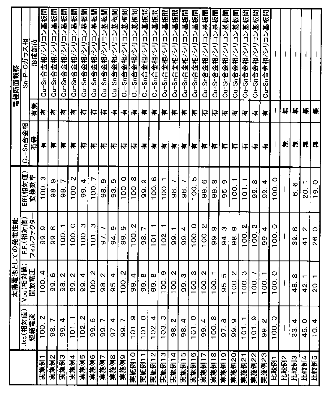
これは例えば以下のように考えられる。比較例4においては、錫含有粒子が含まれていないために、焼成中にシリコン基板と銅の相互拡散が起こり、基板内のpn接合特性が劣化したことが考えられる。また比較例5においては、リン含有銅合金粒子を用いずに純銅(リン含有量が0質量%)を用いたために、焼成中に錫含有粒子と反応する前に銅粒子が酸化し、Cu-Sn合金相が形成されずに電極の抵抗が増加したことが考えられる。


Claims (12)
- リン含有銅合金粒子と、錫含有粒子と、ガラス粒子と、溶剤と、樹脂と、を含む電極用ペースト組成物。
- 前記リン含有銅合金粒子のリン含有率が6質量%以上8質量%以下である請求項1に記載の電極用ペースト組成物。
- 前記錫含有粒子は、錫粒子及び錫含有率が1質量%以上である錫合金粒子から選ばれる少なくとも1種である請求項1又は請求項2に記載の電極用ペースト組成物。
- 前記ガラス粒子は、ガラス軟化点が650℃以下であって、結晶化開始温度が650℃を超える請求項1~請求項3のいずれか1項に記載の電極用ペースト組成物。
- 前記リン含有銅合金粒子と前記錫含有粒子の総含有率を100質量%としたときの前記錫含有粒子の含有率が、5質量%以上70質量%以下である請求項1~請求項4のいずれか1項に記載の電極用ペースト組成物。
- 銀粒子を更に含む請求項1~請求項5のいずれか1項に記載の電極用ペースト組成物。
- 前記リン含有銅合金粒子、前記錫含有粒子及び前記銀粒子の総含有率を100質量%としたときの前記銀粒子の含有率が0.1質量%以上10質量%以下である請求項6に記載の電極用ペースト組成物。
- 前記リン含有銅合金粒子、錫含有粒子及び銀粒子の総含有率が70質量%以上94質量%以下であって、前記ガラス粒子の含有率が0.1質量%以上10質量%以下であって、前記溶剤及び前記樹脂の総含有率が3質量%以上29.9質量%以下である請求項6又は請求項7に記載の電極用ペースト組成物。
- シリコン基板上に付与された請求項1~請求項8のいずれか1項に記載の電極用ペースト組成物を焼成して形成された電極を有する太陽電池素子。
- 前記電極は、Cu-Sn合金相及びSn-P-Oガラス相を含む請求項9に記載の太陽電池素子。
- 前記Sn-P-Oガラス相は、前記Cu-Sn合金相と前記シリコン基板との間に配置されている請求項10に記載の太陽電池素子。
- 請求項9~請求項11のいずれか1項に記載の太陽電池素子と、前記太陽電池素子の電極上に配置されたタブ線とを有する太陽電池。
Priority Applications (3)
| Application Number | Priority Date | Filing Date | Title |
|---|---|---|---|
| CN201180070033.8A CN103477395B (zh) | 2011-04-14 | 2011-04-28 | 电极用糊剂组合物、太阳能电池元件以及太阳能电池 |
| EP11863421.1A EP2698827A4 (en) | 2011-04-14 | 2011-04-28 | ELECTRODE PASTE COMPOSITION, SOLAR CELLS ELEMENT AND SOLAR CELL |
| KR1020137029998A KR101521040B1 (ko) | 2011-04-14 | 2011-04-28 | 전극용 페이스트 조성물, 태양 전지 소자 및 태양 전지 |
Applications Claiming Priority (2)
| Application Number | Priority Date | Filing Date | Title |
|---|---|---|---|
| JP2011-090520 | 2011-04-14 | ||
| JP2011090520A JP5768455B2 (ja) | 2011-04-14 | 2011-04-14 | 電極用ペースト組成物及び太陽電池素子 |
Publications (1)
| Publication Number | Publication Date |
|---|---|
| WO2012140786A1 true WO2012140786A1 (ja) | 2012-10-18 |
Family
ID=47008988
Family Applications (1)
| Application Number | Title | Priority Date | Filing Date |
|---|---|---|---|
| PCT/JP2011/060471 WO2012140786A1 (ja) | 2011-04-14 | 2011-04-28 | 電極用ペースト組成物、太陽電池素子及び太陽電池 |
Country Status (6)
| Country | Link |
|---|---|
| EP (1) | EP2698827A4 (ja) |
| JP (1) | JP5768455B2 (ja) |
| KR (1) | KR101521040B1 (ja) |
| CN (2) | CN103477395B (ja) |
| TW (2) | TWI502609B (ja) |
| WO (1) | WO2012140786A1 (ja) |
Cited By (8)
| Publication number | Priority date | Publication date | Assignee | Title |
|---|---|---|---|---|
| JP2014093491A (ja) * | 2012-11-06 | 2014-05-19 | Hitachi Chemical Co Ltd | 太陽電池素子及びその製造方法、並びに太陽電池 |
| JP2014103220A (ja) * | 2012-11-19 | 2014-06-05 | Hitachi Chemical Co Ltd | 太陽電池及び太陽電池モジュール |
| JP2014103221A (ja) * | 2012-11-19 | 2014-06-05 | Hitachi Chemical Co Ltd | 電極接続セット、太陽電池の製造方法、太陽電池及び太陽電池モジュール |
| CN104021836A (zh) * | 2013-02-28 | 2014-09-03 | 比亚迪股份有限公司 | 一种太阳能电池背电极用金属丝及制备方法、背电极及制备方法、太阳能电池片及电池组件 |
| JPWO2013015172A1 (ja) * | 2011-07-25 | 2015-02-23 | 日立化成株式会社 | 素子及び太陽電池 |
| CN104733546A (zh) * | 2013-12-19 | 2015-06-24 | 日立化成株式会社 | 太阳能电池和太阳能电池模块 |
| JP2017163161A (ja) * | 2017-06-07 | 2017-09-14 | 日立化成株式会社 | 太陽電池及び太陽電池モジュール |
| TWI634668B (zh) * | 2013-12-19 | 2018-09-01 | 日商日立化成股份有限公司 | 太陽電池以及太陽電池模組 |
Families Citing this family (17)
| Publication number | Priority date | Publication date | Assignee | Title |
|---|---|---|---|---|
| JP5120477B2 (ja) * | 2011-04-07 | 2013-01-16 | 日立化成工業株式会社 | 電極用ペースト組成物及び太陽電池 |
| US9224517B2 (en) | 2011-04-07 | 2015-12-29 | Hitachi Chemical Company, Ltd. | Paste composition for electrode and photovoltaic cell |
| JP5720393B2 (ja) * | 2011-04-14 | 2015-05-20 | 日立化成株式会社 | 電極用ペースト組成物、太陽電池素子及び太陽電池 |
| JP2012227183A (ja) * | 2011-04-14 | 2012-11-15 | Hitachi Chem Co Ltd | 電極用ペースト組成物及び太陽電池素子 |
| JP5772174B2 (ja) * | 2011-04-14 | 2015-09-02 | 日立化成株式会社 | 素子及び太陽電池並びに電極用ペースト組成物 |
| TWI574450B (zh) * | 2013-05-13 | 2017-03-11 | 日立化成股份有限公司 | 電極形成用組成物、太陽電池元件及其製造方法、太陽電池及其製造方法 |
| US20160118513A1 (en) * | 2013-05-13 | 2016-04-28 | Hitachi Chemical Company, Ltd. | Composition for forming electrode, photovoltaic cell element and photovoltatic cell |
| JP5766336B1 (ja) * | 2014-06-16 | 2015-08-19 | 株式会社マテリアル・コンセプト | 銅ペーストの焼成方法 |
| JP5958526B2 (ja) * | 2014-11-26 | 2016-08-02 | 日立化成株式会社 | 素子及び太陽電池並びに電極用ペースト組成物 |
| JP2015130355A (ja) * | 2015-02-16 | 2015-07-16 | 日立化成株式会社 | 電極用ペースト組成物及び太陽電池素子 |
| JP6433351B2 (ja) * | 2015-03-19 | 2018-12-05 | 株式会社ノリタケカンパニーリミテド | 被覆銅粉末、銅ペースト、および銅導体膜 |
| KR101955759B1 (ko) * | 2016-06-23 | 2019-03-07 | 삼성에스디아이 주식회사 | P형 태양전지 전극 형성용 조성물 및 이를 이용해 제조된 전극 및 p형 태양전지 |
| CN106024101B (zh) * | 2016-08-05 | 2017-08-01 | 洛阳布鲁姆电子科技有限公司 | 一种复合导电陶瓷浆料及其制备方法 |
| CN106128551A (zh) * | 2016-08-30 | 2016-11-16 | 乐凯特科技铜陵有限公司 | 一种高效水性贯穿线路板导电银浆及其制备方法 |
| JP6879035B2 (ja) * | 2017-04-28 | 2021-06-02 | 住友金属鉱山株式会社 | 導電性組成物、導体の製造方法及び電子部品の配線の形成方法 |
| CN110246606A (zh) * | 2019-06-21 | 2019-09-17 | 广州市儒兴科技开发有限公司 | 一种高性能有机载体及其制备方法与其应用的导电浆料 |
| JP7487471B2 (ja) * | 2019-12-13 | 2024-05-21 | 株式会社レゾナック | 金属ペースト、導電体、並びに、貫通電極を有する基体及びその製造方法 |
Citations (14)
| Publication number | Priority date | Publication date | Assignee | Title |
|---|---|---|---|---|
| JPS6457762A (en) * | 1987-08-28 | 1989-03-06 | Kyocera Corp | Photoelectric converting device |
| JPH0529639A (ja) * | 1991-07-25 | 1993-02-05 | Sharp Corp | 太陽電池 |
| JPH05159621A (ja) * | 1991-12-10 | 1993-06-25 | Matsushita Electric Ind Co Ltd | 導電性ペースト |
| JPH11162859A (ja) * | 1997-11-28 | 1999-06-18 | Canon Inc | シリコン結晶の液相成長方法及びそれを用いた太陽電池の製造方法 |
| JP3050064B2 (ja) | 1994-11-24 | 2000-06-05 | 株式会社村田製作所 | 導電性ペースト、この導電性ペーストからなるグリッド電極が形成された太陽電池及びその製造方法 |
| JP2001110232A (ja) * | 1999-10-13 | 2001-04-20 | Murata Mfg Co Ltd | 導電性ペーストおよびそれを用いた半導体セラミック電子部品 |
| JP2004217952A (ja) | 2003-01-09 | 2004-08-05 | Mitsui Mining & Smelting Co Ltd | 表面処理銅粉並びにその表面処理銅粉の製造方法及びその表面処理銅粉を用いた導電性ペースト |
| JP2005314755A (ja) | 2004-04-28 | 2005-11-10 | Mitsui Mining & Smelting Co Ltd | フレーク銅粉及びその製造方法並びに導電性ペースト |
| JP2006313744A (ja) | 2005-04-14 | 2006-11-16 | E I Du Pont De Nemours & Co | 導電性厚膜組成物、電極、およびそれから形成される半導体デバイス |
| JP2009099443A (ja) * | 2007-10-18 | 2009-05-07 | Fukuda Metal Foil & Powder Co Ltd | 導電材ペースト用銅合金粉 |
| JP2009188281A (ja) | 2008-02-08 | 2009-08-20 | Hitachi Ltd | Cu系配線用材料およびそれを用いた電子部品 |
| JP2010161331A (ja) * | 2008-12-12 | 2010-07-22 | Hitachi Ltd | 電極,電極ペースト及びそれを用いた電子部品 |
| JP2010186862A (ja) * | 2009-02-12 | 2010-08-26 | Shin-Etsu Chemical Co Ltd | 太陽電池 |
| JP2011090520A (ja) | 2009-10-22 | 2011-05-06 | Nippon Yunishisu Kk | 鋼板の変形に基づく形状補完装置およびその方法 |
Family Cites Families (9)
| Publication number | Priority date | Publication date | Assignee | Title |
|---|---|---|---|---|
| JPH1162859A (ja) * | 1997-08-07 | 1999-03-05 | Zexel Corp | 横置き型スクロールコンプレッサ |
| JP2000277768A (ja) | 1999-03-25 | 2000-10-06 | Kyocera Corp | 太陽電池の形成方法 |
| JP2004119692A (ja) * | 2002-09-26 | 2004-04-15 | Koa Corp | 抵抗体組成物および抵抗器 |
| JP4863988B2 (ja) * | 2005-01-25 | 2012-01-25 | 積水化学工業株式会社 | 導電性微粒子、及び異方性導電材料 |
| WO2008078374A1 (ja) * | 2006-12-25 | 2008-07-03 | Namics Corporation | 太陽電池用導電性ペースト |
| JP2009146890A (ja) * | 2007-11-20 | 2009-07-02 | Hitoshi Arai | 低温焼付け可能な銅導電性ペースト。 |
| JP2010059469A (ja) * | 2008-09-03 | 2010-03-18 | Asahi Glass Co Ltd | 銅ナノ粒子の製造方法、金属ペーストおよび金属膜を有する物品 |
| US8895460B2 (en) * | 2009-03-27 | 2014-11-25 | Hitachi Powdered Metals Co., Ltd. | Glass composition, electrically conductive paste composition comprising same, electrode wiring member, and electronic component |
| JP2012227183A (ja) * | 2011-04-14 | 2012-11-15 | Hitachi Chem Co Ltd | 電極用ペースト組成物及び太陽電池素子 |
-
2011
- 2011-04-14 JP JP2011090520A patent/JP5768455B2/ja not_active Expired - Fee Related
- 2011-04-28 CN CN201180070033.8A patent/CN103477395B/zh not_active Expired - Fee Related
- 2011-04-28 CN CN201510350967.7A patent/CN105139917A/zh active Pending
- 2011-04-28 EP EP11863421.1A patent/EP2698827A4/en not_active Withdrawn
- 2011-04-28 KR KR1020137029998A patent/KR101521040B1/ko not_active IP Right Cessation
- 2011-04-28 WO PCT/JP2011/060471 patent/WO2012140786A1/ja active Application Filing
-
2012
- 2012-04-12 TW TW101112901A patent/TWI502609B/zh not_active IP Right Cessation
- 2012-04-12 TW TW104114714A patent/TW201533754A/zh unknown
Patent Citations (14)
| Publication number | Priority date | Publication date | Assignee | Title |
|---|---|---|---|---|
| JPS6457762A (en) * | 1987-08-28 | 1989-03-06 | Kyocera Corp | Photoelectric converting device |
| JPH0529639A (ja) * | 1991-07-25 | 1993-02-05 | Sharp Corp | 太陽電池 |
| JPH05159621A (ja) * | 1991-12-10 | 1993-06-25 | Matsushita Electric Ind Co Ltd | 導電性ペースト |
| JP3050064B2 (ja) | 1994-11-24 | 2000-06-05 | 株式会社村田製作所 | 導電性ペースト、この導電性ペーストからなるグリッド電極が形成された太陽電池及びその製造方法 |
| JPH11162859A (ja) * | 1997-11-28 | 1999-06-18 | Canon Inc | シリコン結晶の液相成長方法及びそれを用いた太陽電池の製造方法 |
| JP2001110232A (ja) * | 1999-10-13 | 2001-04-20 | Murata Mfg Co Ltd | 導電性ペーストおよびそれを用いた半導体セラミック電子部品 |
| JP2004217952A (ja) | 2003-01-09 | 2004-08-05 | Mitsui Mining & Smelting Co Ltd | 表面処理銅粉並びにその表面処理銅粉の製造方法及びその表面処理銅粉を用いた導電性ペースト |
| JP2005314755A (ja) | 2004-04-28 | 2005-11-10 | Mitsui Mining & Smelting Co Ltd | フレーク銅粉及びその製造方法並びに導電性ペースト |
| JP2006313744A (ja) | 2005-04-14 | 2006-11-16 | E I Du Pont De Nemours & Co | 導電性厚膜組成物、電極、およびそれから形成される半導体デバイス |
| JP2009099443A (ja) * | 2007-10-18 | 2009-05-07 | Fukuda Metal Foil & Powder Co Ltd | 導電材ペースト用銅合金粉 |
| JP2009188281A (ja) | 2008-02-08 | 2009-08-20 | Hitachi Ltd | Cu系配線用材料およびそれを用いた電子部品 |
| JP2010161331A (ja) * | 2008-12-12 | 2010-07-22 | Hitachi Ltd | 電極,電極ペースト及びそれを用いた電子部品 |
| JP2010186862A (ja) * | 2009-02-12 | 2010-08-26 | Shin-Etsu Chemical Co Ltd | 太陽電池 |
| JP2011090520A (ja) | 2009-10-22 | 2011-05-06 | Nippon Yunishisu Kk | 鋼板の変形に基づく形状補完装置およびその方法 |
Non-Patent Citations (1)
| Title |
|---|
| See also references of EP2698827A4 * |
Cited By (9)
| Publication number | Priority date | Publication date | Assignee | Title |
|---|---|---|---|---|
| JPWO2013015172A1 (ja) * | 2011-07-25 | 2015-02-23 | 日立化成株式会社 | 素子及び太陽電池 |
| JP2014093491A (ja) * | 2012-11-06 | 2014-05-19 | Hitachi Chemical Co Ltd | 太陽電池素子及びその製造方法、並びに太陽電池 |
| JP2014103220A (ja) * | 2012-11-19 | 2014-06-05 | Hitachi Chemical Co Ltd | 太陽電池及び太陽電池モジュール |
| JP2014103221A (ja) * | 2012-11-19 | 2014-06-05 | Hitachi Chemical Co Ltd | 電極接続セット、太陽電池の製造方法、太陽電池及び太陽電池モジュール |
| CN104021836A (zh) * | 2013-02-28 | 2014-09-03 | 比亚迪股份有限公司 | 一种太阳能电池背电极用金属丝及制备方法、背电极及制备方法、太阳能电池片及电池组件 |
| CN104021836B (zh) * | 2013-02-28 | 2017-02-01 | 比亚迪股份有限公司 | 一种太阳能电池背电极用金属丝及制备方法、背电极及制备方法、太阳能电池片及电池组件 |
| CN104733546A (zh) * | 2013-12-19 | 2015-06-24 | 日立化成株式会社 | 太阳能电池和太阳能电池模块 |
| TWI634668B (zh) * | 2013-12-19 | 2018-09-01 | 日商日立化成股份有限公司 | 太陽電池以及太陽電池模組 |
| JP2017163161A (ja) * | 2017-06-07 | 2017-09-14 | 日立化成株式会社 | 太陽電池及び太陽電池モジュール |
Also Published As
| Publication number | Publication date |
|---|---|
| JP2012227184A (ja) | 2012-11-15 |
| TWI502609B (zh) | 2015-10-01 |
| EP2698827A4 (en) | 2014-12-03 |
| EP2698827A1 (en) | 2014-02-19 |
| KR20140007462A (ko) | 2014-01-17 |
| KR101521040B1 (ko) | 2015-05-15 |
| TW201248654A (en) | 2012-12-01 |
| CN105139917A (zh) | 2015-12-09 |
| TW201533754A (zh) | 2015-09-01 |
| JP5768455B2 (ja) | 2015-08-26 |
| CN103477395A (zh) | 2013-12-25 |
| CN103477395B (zh) | 2016-08-17 |
Similar Documents
| Publication | Publication Date | Title |
|---|---|---|
| JP5768455B2 (ja) | 電極用ペースト組成物及び太陽電池素子 | |
| JP5811186B2 (ja) | 電極用ペースト組成物、太陽電池素子及び太陽電池 | |
| WO2012140787A1 (ja) | 電極用ペースト組成物、太陽電池素子及び太陽電池 | |
| JP5120477B2 (ja) | 電極用ペースト組成物及び太陽電池 | |
| JP5891599B2 (ja) | シリコン系太陽電池の電極用ペースト組成物 | |
| JP6206491B2 (ja) | 電極形成用組成物、太陽電池素子及び太陽電池 | |
| WO2013015172A1 (ja) | 素子及び太陽電池 | |
| JP5879793B2 (ja) | 素子の製造方法及び太陽電池の製造方法 | |
| JP5720393B2 (ja) | 電極用ペースト組成物、太陽電池素子及び太陽電池 | |
| JP5772174B2 (ja) | 素子及び太陽電池並びに電極用ペースト組成物 | |
| US20130118573A1 (en) | Paste composition for electrode, photovoltaic cell element, and photovoltaic cell | |
| WO2015115565A1 (ja) | 電極形成用組成物、電極、太陽電池素子及びその製造方法並びに太陽電池 | |
| JP2016189443A (ja) | 電極形成用組成物、電極、太陽電池素子及びその製造方法、並びに太陽電池 | |
| US20120260982A1 (en) | Paste composition for electrode, photovoltaic cell element, and photovoltaic cell | |
| JP2015195223A (ja) | 電極用ペースト組成物、太陽電池素子及び太陽電池 | |
| JP2015144126A (ja) | 電極用ペースト組成物及び太陽電池素子 | |
| JP2015188089A (ja) | 素子及び太陽電池 | |
| JP5408322B2 (ja) | 電極用ペースト組成物及び太陽電池 | |
| JP2016122840A (ja) | 素子及び太陽電池並びに電極用ペースト組成物 | |
| JP2015079975A (ja) | 素子及び太陽電池並びに電極用ペースト組成物 | |
| JP5958526B2 (ja) | 素子及び太陽電池並びに電極用ペースト組成物 | |
| JP5899689B2 (ja) | 素子及び太陽電池 | |
| JP2016054312A (ja) | 素子及び太陽電池 | |
| JP6464669B2 (ja) | 電極形成用組成物、電極、太陽電池素子並びに太陽電池及びその製造方法 | |
| JP2014093491A (ja) | 太陽電池素子及びその製造方法、並びに太陽電池 |
Legal Events
| Date | Code | Title | Description |
|---|---|---|---|
| 121 | Ep: the epo has been informed by wipo that ep was designated in this application |
Ref document number: 11863421 Country of ref document: EP Kind code of ref document: A1 |
|
| NENP | Non-entry into the national phase |
Ref country code: DE |
|
| ENP | Entry into the national phase |
Ref document number: 20137029998 Country of ref document: KR Kind code of ref document: A |
|
| REEP | Request for entry into the european phase |
Ref document number: 2011863421 Country of ref document: EP |
|
| WWE | Wipo information: entry into national phase |
Ref document number: 2011863421 Country of ref document: EP |