WO2012133569A1 - 渦電流センサ - Google Patents
渦電流センサ Download PDFInfo
- Publication number
- WO2012133569A1 WO2012133569A1 PCT/JP2012/058208 JP2012058208W WO2012133569A1 WO 2012133569 A1 WO2012133569 A1 WO 2012133569A1 JP 2012058208 W JP2012058208 W JP 2012058208W WO 2012133569 A1 WO2012133569 A1 WO 2012133569A1
- Authority
- WO
- WIPO (PCT)
- Prior art keywords
- head
- cable
- capacitive element
- amplifier
- impedance
- Prior art date
- Legal status (The legal status is an assumption and is not a legal conclusion. Google has not performed a legal analysis and makes no representation as to the accuracy of the status listed.)
- Ceased
Links
Images


Classifications
-
- G—PHYSICS
- G01—MEASURING; TESTING
- G01D—MEASURING NOT SPECIALLY ADAPTED FOR A SPECIFIC VARIABLE; ARRANGEMENTS FOR MEASURING TWO OR MORE VARIABLES NOT COVERED IN A SINGLE OTHER SUBCLASS; TARIFF METERING APPARATUS; MEASURING OR TESTING NOT OTHERWISE PROVIDED FOR
- G01D5/00—Mechanical means for transferring the output of a sensing member; Means for converting the output of a sensing member to another variable where the form or nature of the sensing member does not constrain the means for converting; Transducers not specially adapted for a specific variable
- G01D5/12—Mechanical means for transferring the output of a sensing member; Means for converting the output of a sensing member to another variable where the form or nature of the sensing member does not constrain the means for converting; Transducers not specially adapted for a specific variable using electric or magnetic means
- G01D5/14—Mechanical means for transferring the output of a sensing member; Means for converting the output of a sensing member to another variable where the form or nature of the sensing member does not constrain the means for converting; Transducers not specially adapted for a specific variable using electric or magnetic means influencing the magnitude of a current or voltage
- G01D5/20—Mechanical means for transferring the output of a sensing member; Means for converting the output of a sensing member to another variable where the form or nature of the sensing member does not constrain the means for converting; Transducers not specially adapted for a specific variable using electric or magnetic means influencing the magnitude of a current or voltage by varying inductance, e.g. by a movable armature
- G01D5/2006—Mechanical means for transferring the output of a sensing member; Means for converting the output of a sensing member to another variable where the form or nature of the sensing member does not constrain the means for converting; Transducers not specially adapted for a specific variable using electric or magnetic means influencing the magnitude of a current or voltage by varying inductance, e.g. by a movable armature by influencing the self-induction of one or more coils
- G01D5/202—Mechanical means for transferring the output of a sensing member; Means for converting the output of a sensing member to another variable where the form or nature of the sensing member does not constrain the means for converting; Transducers not specially adapted for a specific variable using electric or magnetic means influencing the magnitude of a current or voltage by varying inductance, e.g. by a movable armature by influencing the self-induction of one or more coils by movable a non-ferromagnetic conductive element
-
- G—PHYSICS
- G01—MEASURING; TESTING
- G01B—MEASURING LENGTH, THICKNESS OR SIMILAR LINEAR DIMENSIONS; MEASURING ANGLES; MEASURING AREAS; MEASURING IRREGULARITIES OF SURFACES OR CONTOURS
- G01B7/00—Measuring arrangements characterised by the use of electric or magnetic techniques
-
- G—PHYSICS
- G01—MEASURING; TESTING
- G01B—MEASURING LENGTH, THICKNESS OR SIMILAR LINEAR DIMENSIONS; MEASURING ANGLES; MEASURING AREAS; MEASURING IRREGULARITIES OF SURFACES OR CONTOURS
- G01B7/00—Measuring arrangements characterised by the use of electric or magnetic techniques
- G01B7/14—Measuring arrangements characterised by the use of electric or magnetic techniques for measuring distance or clearance between spaced objects or spaced apertures
Definitions
- the present invention relates to an eddy current sensor, and more particularly to an eddy current sensor in which a sensor head and an amplifier circuit are connected by a cable.
- the eddy current sensor is widely used for measuring the distance (gap) between the detected object and the sensor head, and a resonance type eddy current sensor is one having high detection sensitivity.
- a resonant eddy current sensor has a resonance circuit formed by the impedance of the inductance element (coil) of the sensor head and a capacitive element (capacitor) in the amplifier circuit, greatly increasing the measurement sensitivity near a specific gap, It enables gap measurement with high accuracy.
- FIG. 1 is a diagram showing a schematic configuration of a resonance type eddy current sensor.
- the two terminals of the sensor head 10 are connected to the terminals 31 and 32 of the amplifier circuit 30 by the coaxial cable 20.
- the terminal 31 is connected to the ground via the amplifier capacitive element C 1, and via the auxiliary capacitive element C 2 and the oscillation circuit 33 connected in series.
- the terminal 32 is connected to the ground.
- FIG. 2 is a diagram showing a circuit configuration of the resonance type eddy current sensor of FIG.
- the sensor head 10 has an inductance element (coil) LS inside.
- the two terminals 11 and 12 of the inductance element LS are connected to the terminals 31 and 32 of the amplifier circuit 30 via the coaxial cable 20.
- the amplifier capacitive element C1 is connected between the terminal 31 and the terminal 32.
- the auxiliary capacitive element C2 and the oscillation circuit 33 connected in series are connected between the terminal 31 and the terminal 32 in parallel with the amplifier capacitive element C1.
- the output voltage generated at the terminal 31 is amplified and output by an amplifier (not shown).
- This resonant eddy current sensor outputs a voltage waveform in accordance with the entire (total) impedance of the portion indicated by reference numeral 50 including the inductance element LS, the cable 20 and the amplifier capacitance element C1.
- the capacitance values of the amplifier capacitor element C1 and the auxiliary capacitor element C2 can be adjusted to obtain an optimum resonance state.
- the capacitance values of the amplifier capacitive element C1 and the auxiliary capacitive element C2 are adjusted.
- This total impedance Z is expressed as follows.
- the total impedance Z differs depending on the impedance ZS when the cable 20 is short-circuited.
- the ratio of the impedance change of the inductance element LS in the signal is increased and the sensitivity is improved as the impedance ZS at the time of short-circuit is reduced. Therefore, it is desirable that the impedance ZS at the time of short circuit is small. If the cable 20 is lengthened, the impedance of the cable increases, so the ratio of the impedance of the inductance element LS of the sensor head 10 in the total impedance Z decreases, and the measurement resolution decreases.
- the impedance ZS at the time of short-circuit changes due to the cable construction state and the influence of disturbance, and the signal S / N ratio changes accordingly.
- the S / N ratio decreases as the cable 20 becomes longer. Therefore, the length of the cable 20 has a limit.
- Patent Document 1 describes an eddy current sensor in which an amplifier circuit is provided in a sensor head, the change in impedance of the inductance element LS is amplified, and the amplified signal is transmitted via a cable. ing. Since the signal transmitted through the cable is an amplified signal, a signal with a high S / N ratio is obtained.
- the sensor head becomes larger.
- the sensor head is required to be downsized and the cable extended so that the sensor head can be attached at a desired position, and the sensor head provided with the amplifier circuit cannot cope with downsizing.
- An object of the present invention is to realize an eddy current sensor capable of performing measurement without degrading detection sensitivity even when a cable is lengthened without increasing the size of a sensor head.
- the eddy current sensor of the present invention is provided with a head capacitive element connected in parallel to the inductance element in the sensor head.
- the eddy current sensor of the present invention includes a sensor head having an inductance element, a cable connected to both ends of the inductance element of the sensor head, and an amplifier circuit connected between two terminals of the cable.
- the amplifier circuit includes an oscillation circuit and an amplifier capacitive element connected between two terminals of the cable
- the sensor head includes a head capacitive element provided in the inductance element, and the inductance The element, the head capacitive element, the cable, and the amplifier capacitive element form a resonance circuit for an AC signal output from the oscillation circuit.
- the eddy current sensor of the present invention has a configuration in which a part of the amplifier capacitive element is moved to the head capacitive element in the sensor head.
- the circuit can be configured so that fine adjustment is possible. Thereby, even if the sensor head maintains a small shape and the length of the cable is increased, the detection sensitivity does not deteriorate.
- the detection sensitivity does not deteriorate at all even if the impedance varies in the cable portion. Further, since the detection sensitivity is not deteriorated due to the impedance variation in the cable portion, it means that the detection sensitivity is not deteriorated even if the cable is lengthened as much as necessary.
- the head capacitance element is finely adjusted according to the individual difference of the inductance element.
- the capacitance value of a commercially available capacitor is not continuously prepared, only the capacitance value of the jump value is sold, and when trying to build a head capacitance element using a commercially available capacitor, the sensor Many capacitative elements must be embedded in the head, which increases the size. With this, the purpose of “maintaining small size and lengthening the cable length” cannot be realized.
- the capacitive element and the inductance element are connected in parallel, the combined impedance increases.
- the influence of the impedance of the cable can be relatively reduced. This means that the influence of the cable on the detection sensitivity of the sensor can be reduced.
- the impedance also increases.
- the eddy current can be measured with high accuracy even if the length of the cable is increased.
- one capacitive element having a value as large as possible that can be easily obtained is determined within a range that does not exceed all of the assumed capacitance values constituting the resonance state and the inductance of the sensor head. Regardless of the difference, even if the determined capacitive element is incorporated as a head capacitive element, it can be sufficiently adjusted by the amplifier capacitive element, so that the sensor head is manufactured in an easy process without departing from the spirit of the present invention. You can also.
- an eddy current sensor having a long cable and good detection sensitivity can be realized with a small sensor head.
- FIG. 1 is a diagram showing a schematic configuration of a resonance type eddy current sensor.
- FIG. 2 is a diagram showing a circuit configuration of the resonance type eddy current sensor of FIG.
- FIG. 3 is a diagram illustrating a circuit configuration of the eddy current sensor according to the embodiment.
- FIG. 4 shows the result of simulating with the eddy current sensor of the embodiment and the conventional eddy current sensor how much the total impedance fluctuates when the cable impedance fluctuates by 1% at each cable length.
- FIG. FIG. 5 shows the results of simulating the effects of changes in the inductance value of the inductance element LS on the total impedance at each cable length using the eddy current sensor of the embodiment and the conventional eddy current sensor.
- FIG. FIG. 6 is a diagram illustrating an example of attachment of the inductance element and the capacitive element in the sensor head.
- FIG. 3 is a diagram illustrating a circuit configuration of the eddy current sensor according to the embodiment.
- the eddy current sensor of the embodiment has a schematic configuration as shown in FIG. 1, and the circuit configuration is different from the conventional example shown in FIG.
- the eddy current sensor of the embodiment includes a sensor head 60, a coaxial cable 20, and an amplifier circuit.
- the two terminals 61 and 62 of the sensor head 60 are connected to the terminals 71 and 72 of the amplifier circuit by the coaxial cable 20.
- an amplifier capacitive element C11 is connected between terminals 71 and 72.
- the auxiliary capacitive element C2 and the oscillation circuit 73 connected in series are connected between the terminals 71 and 72 in parallel with the amplifier capacitive element C11.
- the output voltage generated at the terminal 71 is amplified and output by an amplifier (not shown).
- the sensor head 60 includes an inductance element (coil) LS and a head capacitive element CS connected in parallel to the inductance element LS.
- a connection node between the inductance element LS and the head capacitive element CS is connected to two terminals 61 and 62, respectively, and is connected to the terminals 71 and 72 of the amplifier circuit via the coaxial cable 20.
- the head capacitive element CS is provided in parallel with the inductance element LS of the sensor head 60, unlike the conventional example of FIG. Are the same.
- the capacitance values of the amplifier capacitive element C11 and the auxiliary capacitive element C2 can be adjusted in order to obtain an optimal resonance state. Specifically, a capacitive element having a plurality of capacitance values is provided, and the capacitance value can be adjusted by selecting connection with a switch or the like. Further, the total (total) impedance Z of the portion indicated by reference numeral 80 is expressed as follows using the above-described function Para (a, b).
- the output voltage is affected by the output impedance of the oscillation circuits 33 and 73 and the input impedance of the detection circuit, and is not essential. Therefore, in this simulation, a more essential total impedance is verified.
- the optimum value of the auxiliary capacitance element C2 fluctuates depending on the output impedance of the oscillation circuits 33 and 73, the input impedance of the detection circuit, the input range of the detection circuit, and the like.
- the second item is a simulation of how the influence of the change in the inductance value of the inductance element LS appears in the total impedance for each cable length.
- a larger fluctuation means higher sensitivity and improved S / N.
- the inductance value of the inductance element LS is assumed to vary from 12 ⁇ H to 13 ⁇ H based on the actual inductance of the sensor head.
- the capacitance value of the head capacitive element CS was 6800 pF.
- the impedance Z1 of the amplifier capacitor C1 is selected to be
- 4/3 ⁇
- the impedance Z11 of the amplifier capacitor C11 is such that when the inductance value of the inductance element LS is 12 ⁇ H, the conventional example of FIG. 2 and the total impedance Z of the present embodiment of FIG. Selected. Specifically, the capacitance value of the amplifier capacitor C11 is adjusted with 791 pF when the cable length is 1 m and 229 pF when the cable length is 10 m as the center, and the middle value is centered on the value between them. As adjusted.
- FIG. 4 shows the simulation results for the first item, where reference characters A to C are the case of this embodiment, A is a cable length of 3.5 m, and B is a cable length of 6.0 m. Respectively, when C is a cable length of 10.0 m.
- Reference numerals D to F in the case of the conventional example of FIG. 2 show a case where D is a cable length of 3.5 m, E is a cable length of 6.0 m, and F is a cable length of 10.0 m.
- the variation rate of the total impedance is smaller in the present embodiment than in the conventional example of FIG. This means that the present embodiment is more resistant to uncertain elements (variations) in the cable portion than the conventional example.
- FIG. 5 shows simulation results for the second item described above, where reference characters A to C are the case of this embodiment, A is a cable length of 3.5 m, and B is a cable length of 6.0 m. Respectively, when C is a cable length of 10.0 m.
- Reference numerals D to F in the case of the conventional example of FIG. 2 show a case where D is a cable length of 3.5 m, E is a cable length of 6.0 m, and F is a cable length of 10.0 m.
- the variation rate of the total impedance with respect to the change of the inductance value of the inductance element LS is larger in the present embodiment than in the conventional example of FIG. This means that the present embodiment is more sensitive to changes in the inductance element LS than the conventional example, and the S / N is improved.
- the characteristics are improved at any cable length. That is, the influence of cable impedance can be reduced.
- the inductance element LS and the head capacitor element CS are connected in parallel in the sensor head 60, the combined impedance increases, and the influence of the impedance of the cable 20 can be relatively reduced.
- the combination of the capacitance value of the head capacitive element CS and the capacitance value of the amplifier capacitive element C11 is relatively flexible while maintaining the sum of the capacitance value of the amplifier capacitive element C11 and the capacitance value of the head capacitive element CS. Therefore, a general-purpose small capacitive element can be selected as the head capacitive element CS, and a circuit can be configured so that the amplifier capacitive element C11 can be finely adjusted. Thereby, even if the sensor head 60 maintains a small shape and lengthens the cable 20, detection sensitivity does not deteriorate. In addition, the ideal measurement state of the sensor is maintained.
- the conventional amplifier circuit can be used as it is, or even when the amplifier capacitance element is changed, the change of the amplifier capacitance element is small. It can be handled only by a change in scale.
- the ratio of the capacitance value of the head capacitive element CS to the capacitive value of the amplifier capacitive element C11 is as follows.
- the larger the value, the more effective, and the capacity of the head capacitive element CS is preferably greater than or equal to the capacity of the amplifier capacitive element C11, and the capacity of the head capacitive element is desirably 5 times or more that of the amplifier capacitive element.
- the stray capacitance inside the sensor head is very small (about 2 pF in the sensor head used as an example of the simulation in the present embodiment), and the stray capacitance has a head capacitance element CS in the present embodiment. Even if is replaced, a significant difference from the configuration of the conventional example shown in FIG. 2 cannot be clearly obtained. In addition, the capacitance value of the stray capacitance cannot be stabilized at the same level as that of the circulating capacitors (tolerance 2% or less, temperature characteristic 60 ppm / ° C or less).
- this embodiment describes the apparatus which detects the distance with to-be-detected body
- the application range of this invention is not the limitation.
- the inductance around the sensor head changes due to changes in the posture, internal composition, quenching state, shape, magnetization, etc. of the detection body (that is, when the impedance of the inductance element LS changes)
- the present invention can also be applied to a measuring device that detects the above.
- the cable 20 is assumed to be coaxial, but the same effect is naturally obtained with respect to other types of cables as well as the coaxial.
- the number of elements constituting the head capacitive element may be plural as long as the size of the sensor head is not affected.
- the head capacitance element is not limited to “the largest capacitance among commercially available capacitors having a capacitance value equal to or less than that of the amplifier capacitance element”. For example, even if an element having a capacitance slightly smaller than the largest one is used to secure a margin for the resonance state, it is obvious that the purpose of this patent can be sufficiently achieved.
- FIG. 6A and 6B are diagrams for explaining an example of attachment of the inductance element and the capacitive element in the sensor head.
- FIG. 6A shows a conventional example of attachment
- FIG. 6B shows an example of attachment of the embodiment.
- the sensor head 10 has a cylindrical bobbin 91, and a cylindrical groove 92 is formed near the tip of the bobbin 91. As shown in FIG. A coil 93 formed by winding a shield wire around the groove 92 forms an inductance element LS. Both terminals 94 and 95 of the shield wire are connected to the cable 20.
- a coil in a small sensor head is very small, and it is difficult to fix a wire drawn from the coil. If the wire drawn from the coil cannot be fixed, the coil wound around the bobbin will be broken, resulting in a serious problem in the characteristics of the sensor head.
- a capacitor which is a general capacitive element CS has two electrodes. As shown in FIG. 3, both terminals of the inductance element LS in the sensor head 60 are connected to respective electrodes of the capacitor CS. Therefore, as shown in FIG. 6B, a through hole 96 is provided in the bobbin 91, and a capacitor 97 is fixed in the through hole 96, and the electrodes 98 and 99 on both sides of the capacitor 97 are near the cylindrical surface of the bobbin 91. To be located. Then, the wires 94 and 95 of both terminals of the inductance element are connected and fixed to the electrodes 98 and 99. Electrodes 98 and 99 are further connected to a line of cable 20 (not shown).
- the assembly of the sensor head 60 is facilitated, and the wires 94 and 95 of both terminals are fixed, so that the possibility that the coil will collapse can be easily eliminated.
- the capacitor 97 can be easily fixed and connected to the capacitor 97. Since the lines 94 and 95 to be separated can be separated on the opposite side of the bobbin 91, workability is improved and unwanted contact errors can be prevented.
- the present invention is applicable to a resonance type eddy current sensor.
Landscapes
- Physics & Mathematics (AREA)
- General Physics & Mathematics (AREA)
- Measurement Of Length, Angles, Or The Like Using Electric Or Magnetic Means (AREA)
- Transmission And Conversion Of Sensor Element Output (AREA)
Abstract
小型のセンサヘッドで、ケーブルが長く、検出感度の良好な渦電流センサが開示され、インダクタンス素子LS を有するセンサヘッド60 と、センサヘッド60 のインダクタンス素子LS の両端に接続されるケーブル20 と、ケーブル20 の2つの端子間に接続されるアンプ回路と、を備え、アンプ回路は、発振回路73 と、ケーブル20 の2つの端子間に接続されるアンプ容量素子C11 と、を備え、センサヘッド60 は、インダクタンス素子LS に設けられたヘッド容量素子CS を有し、インダクタンス素子LS、ヘッド容量素子CS、ケーブル20およびアンプ容量素子C11 は、発振回路の出力する交流信号に対する共振回路を形成する。
Description
本発明は、渦電流センサに関し、特にセンサヘッドとアンプ回路の間をケーブルで接続した渦電流センサに関する。
渦電流センサは、被検出体とセンサヘッドとの間の距離(ギャップ)を測定するために広く使用されており、高検出感度のものに共振型の渦電流センサがある。共振型の渦電流センサには、センサヘッドのインダクタンス素子(コイル)によるインピーダンスとアンプ回路内の容量素子(コンデンサ)で共振回路を形成し、特定のギャップ近傍での測定感度を大幅に増加させ、高精度でのギャップ測定を可能にしている。
図1は、共振型の渦電流センサの概略構成を示す図である。
センサヘッド10の2個の端子は、同軸ケーブル20により、アンプ回路30の端子31および32に接続される。アンプ回路30内では、端子31は、アンプ容量素子C1を介して、および直列に接続された補助容量素子C2および発振回路33を介して、グランドに接続される。端子32は、グランドに接続される。
センサヘッド10の2個の端子は、同軸ケーブル20により、アンプ回路30の端子31および32に接続される。アンプ回路30内では、端子31は、アンプ容量素子C1を介して、および直列に接続された補助容量素子C2および発振回路33を介して、グランドに接続される。端子32は、グランドに接続される。
図2は、図1の共振型の渦電流センサの回路構成を示す図である。
センサヘッド10は、内部にインダクタンス素子(コイル)LSを有する。インダクタンス素子LSの2個の端子11および12は、同軸ケーブル20を介して、アンプ回路30の端子31および32に接続される。アンプ容量素子C1は、端子31と端子32の間に接続される。直列に接続された補助容量素子C2および発振回路33は、端子31と端子32の間に、アンプ容量素子C1と並列に接続される。端子31に発生する出力電圧は、図示していない増幅器により増幅されて出力される。
センサヘッド10は、内部にインダクタンス素子(コイル)LSを有する。インダクタンス素子LSの2個の端子11および12は、同軸ケーブル20を介して、アンプ回路30の端子31および32に接続される。アンプ容量素子C1は、端子31と端子32の間に接続される。直列に接続された補助容量素子C2および発振回路33は、端子31と端子32の間に、アンプ容量素子C1と並列に接続される。端子31に発生する出力電圧は、図示していない増幅器により増幅されて出力される。
この共振型の渦電流センサは、インダクタンス素子LS、ケーブル20およびアンプ容量素子C1を含んだ参照番号50で示す部分の全体(トータル)インピーダンスに応じて電圧波形が出力される。インダクタンス素子LSやケーブル20のインピーダンス特性の個体差等のため、最適な共振状態を得るには、アンプ容量素子C1および補助容量素子C2の容量値を調整可能にし、最適な共振状態が得られるようにアンプ容量素子C1および補助容量素子C2の容量値を調整する。このトータルインピーダンスZは、次のように表される。
まず、次の式1で表される関数Para(a,b)を定義する。

図2の参照番号50で示す部分のトータルインピーダンスZは、次の式2で表される。
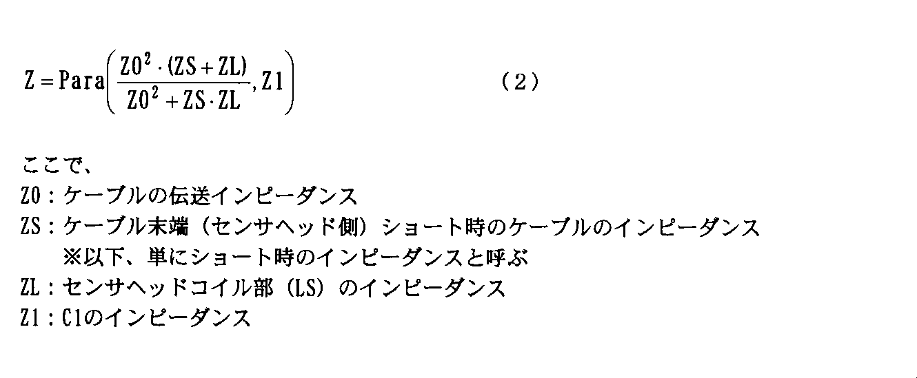
上記の式から明らかなように、トータルインピーダンスZは、ケーブル20のショート時のインピーダンスZSに応じて異なる。
ギャップの測定は、センサヘッド10のインダクタンス素子LSのインピーダンス変化を検出することにより行うため、ショート時のインピーダンスZSが小さいほど、信号におけるインダクタンス素子LSのインピーダンス変化の割合が大きくなり、感度が向上するため、ショート時のインピーダンスZSは小さいことが望ましい。
ケーブル20を長くすると、ケーブルのインピーダンスが増加するため、トータルインピーダンスZにおけるセンサヘッド10のインダクタンス素子LSのインピーダンスの割合が減少し、測定分解能が低下する。
ケーブル20を長くすると、ケーブルのインピーダンスが増加するため、トータルインピーダンスZにおけるセンサヘッド10のインダクタンス素子LSのインピーダンスの割合が減少し、測定分解能が低下する。
また、ケーブルの施工状態や外乱の影響により、ショート時のインピーダンスZSが変化し、それに応じて信号のS/N比が変化する。一般にケーブル20が長くなるほどS/N比が低下する。そのため、ケーブル20の長さには限界がある。
一方、インダクタンス素子LSのインダクタンスを増加させるなどして、センサヘッド10のインピーダンスを増加させて、測定分解能を向上することが考えられるが、そのような対策は、センサの特性を変化させ、センサの理想的な測定状態から外れるという問題を発生する。
このような問題を解決するために、特許文献1は、センサヘッドにアンプ回路を設け、インダクタンス素子LSのインピーダンスの変化を増幅し、増幅した信号をケーブルを介して伝送する渦電流センサを記載している。ケーブルで伝送される信号は、増幅された信号であるため、S/N比の高い信号が得られる。
しかし、センサヘッドにアンプ回路を設けると、センサヘッドが大型化する。センサヘッドは、所望の位置に取り付けられるように、小型化とケーブルの延長が求められており、アンプ回路を設けたセンサヘッドでは小型化に対応できない。
本発明は、センサヘッドを大型化すること無しに、ケーブルを長くしても検出感度を劣化させずに測定が可能な渦電流センサの実現を目的とする。
上記課題を解決するため、本発明の渦電流センサは、センサヘッドに、インダクタンス素子に並列に接続されるヘッド容量素子を設ける。
すなわち、本発明の渦電流センサは、インダクタンス素子を有するセンサヘッドと、前記センサヘッドの前記インダクタンス素子の両端に接続されるケーブルと、前記ケーブルの2つの端子間に接続されるアンプ回路と、を備え、前記アンプ回路は、発振回路と、前記ケーブルの2つの端子間に接続されるアンプ容量素子と、を備え、前記センサヘッドは、前記インダクタンス素子に設けられたヘッド容量素子を備え、前記インダクタンス素子、前記ヘッド容量素子、前記ケーブルおよび前記アンプ容量素子は、前記発振回路の出力する交流信号に対する共振回路を形成することを特徴とする。
本発明の渦電流センサは、アンプ容量素子の一部をセンサヘッド内のヘッド容量素子に移した構成を有する。インダクタンス素子と並列にヘッド容量素子を接続することにより、合成のインピーダンスが大きくなり、相対的にケーブルのインピーダンスの影響を低減できる。ヘッド容量素子の容量値は、インダクタンス素子との共振状態を構成する容量値に近ければ近いほど良い。
また、アンプ容量素子の容量値とヘッド容量素子の容量値の和を維持すれば、センサの理想的な測定状態から外れるという問題は発生しない。そして、上記の条件で、ヘッド容量素子の容量値とアンプ容量素子の容量値の組合せには比較的自由度があるので、ヘッド容量素子は汎用の小型の容量素子を選択し、アンプ容量素子は微調整可能なように回路を構成することができる。これにより、センサヘッドは小型の形状を維持して、ケーブルの長さを長くしても、検出感度は劣化しない。
理論上は、アンプ容量素子の容量の全てをヘッド容量素子へ移動することにより、センサヘッド内においてインダクタンス素子とヘッド容量素子が完全な共振状態を構築することができる(すなわちインダクタンス素子とヘッド容量素子の合成インピーダンスが無限大となる)。これにより、ケーブルのインピーダンスの比率が、インダクタンス素子とヘッド容量素子の合成のインピーダンスに対して、限りなく小さくなり、すなわち検出感度に対するケーブルの影響が限りなく小さくなる。これは、ケーブルの部分でインピーダンスの変動が生じても、検出感度が全く劣化しないことを意味する。また、ケーブルの部分でのインピーダンスの変動により検出感度が劣化しないのだから、ケーブルを必要なだけ長くしてもやはり、検出感度が劣化しないことを意味する。
但し、センサヘッド内のインダクタンス素子のインピーダンス値には個体差があり、図2の構成と同様の共振状態を構築するためには、インダクタンス素子の個体差に応じて、ヘッド容量素子を微調整しなければならない。市販のコンデンサ(容量素子)の容量値は連続的には準備されておらず、飛び飛びの値の容量値のみ販売されており、市販のコンデンサを用いて、ヘッド容量素子を構築しようとすると、センサヘッド内に多数の容量素子を埋め込まなければならず、大型化してしまう。これでは、「小型を維持し、かつケーブル長を長くする」という目的を実現することはできない。
そこで、アンプ容量素子の容量の全てをヘッド容量素子へ移動するのではなく、できるだけ多くの容量をヘッド容量へ移動することが現実的である。すなわち、アンプ容量素子以下の容量値で、かつ容易に入手可能な市販のコンデンサのうち、最も大きな容量のもの1個をヘッド容量素子とする。この場合、ヘッド容量素子1個だけではインダクタンス素子との共振状態を構成できないので、その差を埋めるために若干のアンプ容量素子を設ける。すなわち、ヘッド容量素子とアンプ容量素子との和が、インダクタンス素子と共振状態を構成するようにする。アンプ側にはスペース的な余裕があるため、多数の容量素子による調整回路等を設けることが可能である。
容量素子とインダクタンス素子を並列に接続すると、その合成インピーダンスは大きくなる。ヘッド容量素子をセンサヘッドのインダクタンス素子に並列に接続し、その合成インピーダンスを大きくすることにより、相対的にケーブルのインピーダンスの影響を低減できる。これは、センサの検出感度に対するケーブルの影響を低減できること意味する。ケーブルを長くすると、そのインピーダンスも増加するが、上記の方法でケーブルのインピーダンスの影響を低減することにより、ケーブルを長くしても、高精度での渦電流測定を可能とすることができる。
前述のとおり、センサヘッドのインダクタンス素子のインダクタンスには個体差がある。そこで、センサヘッドのインダクタンスと共振状態を構成する想定される全ての容量値を越えない範囲で、容易に入手可能なできるだけ大きな値の容量素子を1つ決定しておき、センサヘッドのインダクタンスの個体差によらず、その決定した容量素子をヘッド容量素子として組み込んでおいても、アンプ容量素子で充分に調整可能であるので、本発明の趣旨に反せず、容易な工程でセンサヘッドを製造することもできる。
本発明によれば、小型のセンサヘッドで、ケーブルが長く、検出感度の良好な渦電流センサが実現される。
図3は、実施形態の渦電流センサの回路構成を示す図である。
実施形態の渦電流センサは、図1に示すような概略構成を有し、回路構成が図2に示した従来例と異なる。
実施形態の渦電流センサは、図1に示すような概略構成を有し、回路構成が図2に示した従来例と異なる。
実施形態の渦電流センサは、センサヘッド60と、同軸ケーブル20と、アンプ回路と、を有する。センサヘッド60の2個の端子61および62は、同軸ケーブル20により、アンプ回路の端子71および72に接続される。アンプ回路内では、アンプ容量素子C11が端子71と72の間に接続される。さらに直列に接続された補助容量素子C2および発振回路73が、アンプ容量素子C11と並列に、端子71と72の間に接続される。端子71に発生する出力電圧は、図示していない増幅器により増幅されて出力される。
センサヘッド60は、内部にインダクタンス素子(コイル)LSと、インダクタンス素子LSに並列に接続されたヘッド容量素子CSと、を有する。インダクタンス素子LSとヘッド容量素子CSの接続ノードは、2個の端子61および62にそれぞれ接続され、同軸ケーブル20を介して、アンプ回路の端子71および72に接続される。
図3を図2と比較して明らかなように、実施形態では、センサヘッド60のインダクタンス素子LSと並列に、ヘッド容量素子CSを設けたことが、図2の従来例と異なり、他の部分は、同じである。言い換えれば、実施形態の渦電流センサは、アンプ容量素子の一部をセンサヘッド内のヘッド容量素子CSに移した構成を有する。したがって、図2のアンプ容量素子C1と、図3のアンプ容量素子C11およびヘッド容量素子CSの容量値は、基本的には、C1=C11+CSの関係を有する。(ただし、ケーブルは分布定数回路等で近似される複雑なインピーダンス特性を有するため、最適な特性を得るためのC11は、厳密にはC1=C11+CSの関係から多少は異なる場合があり得る。)
前述のように、アンプ容量素子C11および補助容量素子C2は、最適な共振状態を得るために、容量値を調整可能にしている。具体的には、複数の容量値を有する容量素子を設け、スイッチ等で接続を選択して容量値を調整可能にしている。
また、参照番号80で示す部分の全体(トータル)インピーダンスZは、前述の関数Para(a,b)を利用して次のように表される。
また、参照番号80で示す部分の全体(トータル)インピーダンスZは、前述の関数Para(a,b)を利用して次のように表される。
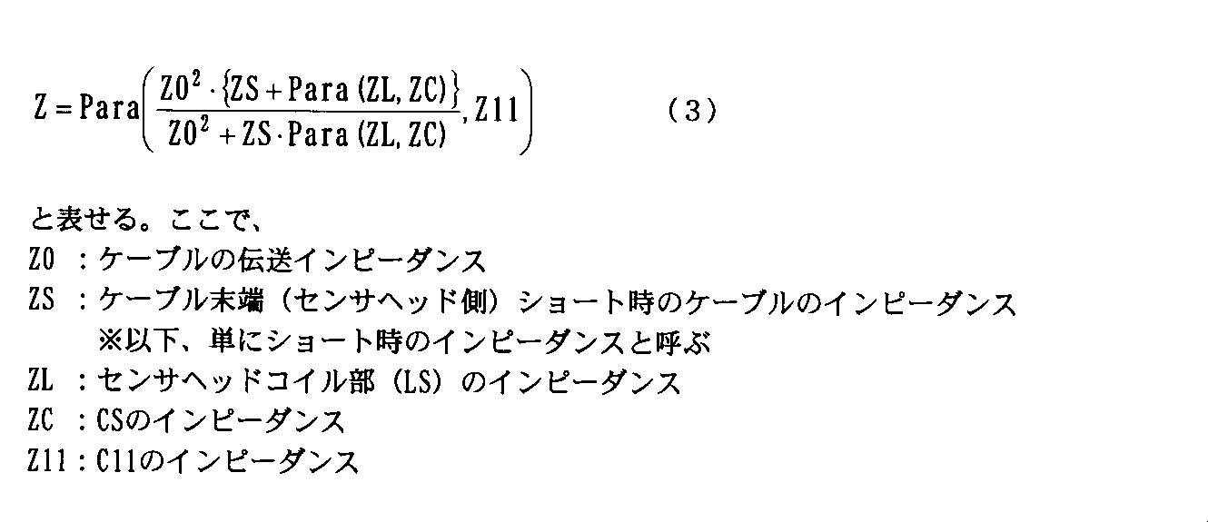
上記の式に基づいて、以下の条件のもとに、ケーブルのインピーダンス(ショート時のインピーダンス)が、トータルインピーダンスへどのように影響するかを、図2の従来例と図3の本実施形態とで比較を行った。
出力電圧は、発振回路33、73の出力インピーダンスや検波回路の入力インピーダンスの影響を受け、本質的ではないため、本シミュレーションでは、より本質的なトータルインピーダンスについて検証することとした。
また、補助容量素子C2は、発振回路33、73の出力インピーダンスや検波回路の入力インピーダンス、検波回路の入力レンジ等により最適値が変動し、本質的ではないため、やはり本シミュレーションから除外した。
比較は、次の2項目について行った。
(1)第1の項目は、それぞれのケーブル長において、ケーブルインピーダンスが、1%変動した場合に、トータルインピーダンスがどの程度変動するかをシミュレーションした。この場合、変動が少ない方が、ケーブル部の不確定要素(変動)に対する耐性が強いと考えられるので、変動が少なければ改善したことを意味する。
(1)第1の項目は、それぞれのケーブル長において、ケーブルインピーダンスが、1%変動した場合に、トータルインピーダンスがどの程度変動するかをシミュレーションした。この場合、変動が少ない方が、ケーブル部の不確定要素(変動)に対する耐性が強いと考えられるので、変動が少なければ改善したことを意味する。
(2)第2の項目は、それぞれのケーブル長において、インダクタンス要素LSのインダクタンス値の変化の影響が、トータルインピーダンスにどのように現れるかをシミュレーションした。この場合、変動が大きい方が、感度が大きく取れ、S/Nが改善することを意味する。
シミュレーションの条件は、以下の通りである。
周波数f=455kHz
Z0(ケーブルの伝送インピーダンス)=50Ω
周波数f=455kHz
Z0(ケーブルの伝送インピーダンス)=50Ω
ショート時のインピーダンスZSは、ケーブル長により異なり、実在するケーブルの実測値をもとに、ケーブル長=3.5mの時ZS=j3.07Ω、ケーブル長=6.0mの時ZS=j5.01Ω、ケーブル長=10.0mの時ZS=j8.57Ωとした。ただし、計算を簡単にするため、インピーダンスの位相は90°であるものとした。
インダクタンス素子LSのインダクタンス値は、実在するセンサヘッドのインダクタンスをもとに、12μH~13μHで変化するとした。
インダクタンス素子LSのインダクタンス値は、実在するセンサヘッドのインダクタンスをもとに、12μH~13μHで変化するとした。
ヘッド容量素子CSの容量値は、6800pFとした。
図2の従来例では、アンプ容量C1のインピーダンスZ1は、|Z1|=4/3×|Z|となるように選んだ。
図2の従来例では、アンプ容量C1のインピーダンスZ1は、|Z1|=4/3×|Z|となるように選んだ。
図3の本実施形態においては、アンプ容量C11のインピーダンスZ11は、インダクタンス素子LSのインダクタンス値=12μHである場合に、図2の従来例と図3の本実施形態のトータルインピーダンスZが一致するように選択した。具体的には、アンプ容量C11の容量値は、ケーブル長が1mの時には791pFを、ケーブル長が10mの時には229pFを、それぞれ中心として調整し、中間の長さのケーブルについてはその間の値を中心として調整した。
図4は、上記の第1の項目についてのシミュレーション結果を示し、参照符号A~Cが本実施形態の場合で、Aがケーブル長3.5mの場合を、Bがケーブル長6.0mの場合を、Cがケーブル長10.0mの場合を、それぞれ示す。参照符号D~Fが図2の従来例の場合で、Dがケーブル長3.5mの場合を、Eがケーブル長6.0mの場合を、Fがケーブル長10.0mの場合を、示す。対応するケーブル長で、トータルインピーダンスの変動率は、本実施形態における方が、図2の従来例におけるより小さくなっている。これは、本実施形態の方が従来例に比べて、ケーブル部の不確定要素(変動)に対する耐性が強いことを意味する。
図5は、上記の第2の項目についてのシミュレーション結果を示し、参照符号A~Cが本実施形態の場合で、Aがケーブル長3.5mの場合を、Bがケーブル長6.0mの場合を、Cがケーブル長10.0mの場合を、それぞれ示す。参照符号D~Fが図2の従来例の場合で、Dがケーブル長3.5mの場合を、Eがケーブル長6.0mの場合を、Fがケーブル長10.0mの場合を、示す。対応するケーブル長で、インダクタンス要素LSのインダクタンス値の変化に対するトータルインピーダンスの変動率は、本実施形態における方が、図2の従来例におけるより大きくなっている。これは、本実施形態の方が従来例に比べて、インダクタンス要素LSの変化に対して感度がよく、S/Nが改善することを意味する。
以上説明したように、本実施形態によれば、第1および第2の項目についてのシミュレーション結果では、いずれのケーブル長でも特性は改善している。すなわち、ケーブルインピーダンスの影響を低減することができる。
本実施形態のように、センサヘッド60において、インダクタンス素子LSとヘッド容量素子CSを並列接続すると、合成のインピーダンスが大きくなり、相対的にケーブル20のインピーダンスの影響を低減できる。
また、アンプ容量素子C11の容量値とヘッド容量素子CSの容量値の和を維持した上で、ヘッド容量素子CSの容量値とアンプ容量素子C11の容量値の組合せには比較的自由度があるので、ヘッド容量素子CSは汎用の小型の容量素子を選択し、アンプ容量素子C11は微調整可能なように回路を構成することができる。これにより、センサヘッド60は小型の形状を維持して、ケーブル20の長さを長くしても、検出感度は劣化しない。また、センサの理想的な測定状態が維持される。
さらに、アンプ回路側のアンプ容量素子C11は、容量値が小さくなるだけで、回路構成自体は変わらないので、従来のアンプ回路をそのまま使用できるか、変更する場合でもアンプ容量素子の変更等の小規模な変更だけで対応可能である。
上記のように、図2のアンプ容量素子C1の一部をセンサヘッド60内のヘッド容量素子CSに移した構成であり、アンプ容量素子C11の容量値に対するヘッド容量素子CSの容量値の比率は大きいほど効果があり、ヘッド容量素子CSの容量は、アンプ容量素子C11の容量以上であることが望ましく、さらにヘッド容量素子の容量は、アンプ容量素子の5倍以上であることが望ましい。
なお、センサヘッド内部(コイル部)の浮遊容量は、非常に小さく(本実施形態でのシミュレーションの実例として用いたセンサヘッドでは約2pFである)、浮遊容量をもって、本実施形態におけるヘッド容量素子CSを置き換えても、図2に記載した従来例の構成に対する優位な差は、明らかに得られない。また、浮遊容量の容量値を、流通しているコンデンサ(許容差2%以下、温度特性60ppm/°C以下)と同等レベルで安定させることもできない。
なお、本実施形態は、被検出体との距離を検出する装置について述べているが、本発明の適用範囲はその限りではない。例えば、検出体の姿勢や内部組成、焼き入れの状態、形状、磁化等の変化により、センサヘッド周辺のインダクタンスが変化する場合(すなわち、インダクタンス素子LSのインピーダンスが変化する場合)は、それらの変化を検出する測定装置にも、本発明を適用することができる。
なお、本実施形態では、ケーブル20は同軸であるとしているが、同軸に限らず他の種類のケーブルについても当然同様の効果が得られる。
なお、ヘッド容量素子を構成する素子数は、センサヘッドの大きさに影響を与えない範囲で、複数個であっても良い。
なお、ヘッド容量素子は、「アンプ容量素子以下の容量値で、かつ容易に入手可能な市販のコンデンサのうち、最も大きな容量のも」に限られるものではない。たとえば、共振状態に対するマージンを確保するために、最も大きなものより若干小さな容量の素子を用いたとしても、本特許の趣旨が充分達成できることは自明である。
なお、ヘッド容量素子は、「アンプ容量素子以下の容量値で、かつ容易に入手可能な市販のコンデンサのうち、最も大きな容量のも」に限られるものではない。たとえば、共振状態に対するマージンを確保するために、最も大きなものより若干小さな容量の素子を用いたとしても、本特許の趣旨が充分達成できることは自明である。
図6は、センサヘッドにおけるインダクタンス素子および容量素子の取り付け例を説明する図であり、(A)が従来の取り付け例を、(B)が実施形態の取り付け例を示す。
図6の(A)に示すように、従来例では、センサヘッド10は、円筒状のボビン91を有し、ボビン91の先端付近に円筒状の溝92が形成されている。溝92にシールド線を巻いて形成したコイル93が、インダクタンス素子LSをなす。シールド線の両端子94および95が、ケーブル20に接続される。
一般に、小型のセンサヘッド内のコイルは微小であり、コイルから引き出された線を固定するには、困難さが伴う。コイルから引き出された線が固定できないと、ボビンに巻かれたコイルが崩れてしまうことになり、センサヘッドの特性に重大な不具合が発生することになる。
一般的な容量素子CSであるコンデンサは、2つの電極を有している。図3に示すように、センサヘッド60内のインダクタンス素子LSの両端子は、コンデンサCSのそれぞれの電極に接続されることになる。そこで、図6の(B)に示すように、ボビン91に貫通穴96を設け、貫通穴96内にコンデンサ97を固定して、コンデンサ97の両側の電極98および99がボビン91の円筒表面付近に位置するようにする。そして、インダクタンス素子の両端子の線94および95を、電極98および99に接続して固定する。電極98および99は、ケーブル20の線(図示せず)にさらに接続される。これにより、センサヘッド60の組立が容易となり、両端子の線94および95を固定するので、コイルが崩れてしまう恐れを、容易に解消することができる。さらに、図6の(B)に示すように、ボビン91に小さな貫通穴96をあけておき、コンデンサ97をボビン91に貫通させることにより、容易にコンデンサ97を固定でき、かつ、コンデンサ97に接続する線94および95を、それぞれボビン91の反対側に分離することが出来るため、作業性が向上するとともに、望まない誤接触等を防止することができる。
以上、本発明の実施例を説明したが、各種の変形例が可能であるのはいうまでもない。
例えば、特許文献1の図3で示される容量素子16および17の一部容量だけをインダクタンス素子11と並列となるようにセンサヘッド内部に組み込むようにしてもよい。
例えば、特許文献1の図3で示される容量素子16および17の一部容量だけをインダクタンス素子11と並列となるようにセンサヘッド内部に組み込むようにしてもよい。
本発明は、共振型の渦電流センサに適用可能である。
10、60 センサヘッド
20 ケーブル
71.72 端子
73 発振回路
LS インダクタンス素子
CS ヘッド容量素子
C11 アンプ容量素子
C2 補助容量素子
20 ケーブル
71.72 端子
73 発振回路
LS インダクタンス素子
CS ヘッド容量素子
C11 アンプ容量素子
C2 補助容量素子
Claims (5)
- インダクタンス素子を有するセンサヘッドと、
前記センサヘッドの前記インダクタンス素子の両端に接続されるケーブルと、
前記ケーブルの2つの端子間に接続されるアンプ回路と、を備え、
前記アンプ回路は、発振回路と、前記ケーブルの2つの端子間に接続されるアンプ容量素子と、を備え、
前記センサヘッドは、前記インダクタンス素子に設けられたヘッド容量素子を備え、
前記インダクタンス素子、前記ヘッド容量素子、前記ケーブルおよび前記アンプ容量素子は、前記発振回路の出力する交流信号に対する共振回路を形成することを特徴とする渦電流センサ。 - 前記インダクタンス素子は、被測定物との距離によってインピーダンスが変化する請求項1記載の渦電流センサ。
- 前記ヘッド容量素子は、小数の容量素子のみで構成される、請求項2記載の渦電流センサ。
- 前記ヘッド容量素子は、1個の容量素子のみで構成される、請求項2記載の渦電流センサ。
- 前記ヘッド容量素子は、一定の容量の1個ないし小数の容量素子のみで構成される、請求項2の渦電流センサ。
Priority Applications (1)
| Application Number | Priority Date | Filing Date | Title |
|---|---|---|---|
| JP2013507688A JP5968305B2 (ja) | 2011-03-31 | 2012-03-28 | 渦電流センサ |
Applications Claiming Priority (2)
| Application Number | Priority Date | Filing Date | Title |
|---|---|---|---|
| JP2011077298 | 2011-03-31 | ||
| JP2011-077298 | 2011-03-31 |
Publications (1)
| Publication Number | Publication Date |
|---|---|
| WO2012133569A1 true WO2012133569A1 (ja) | 2012-10-04 |
Family
ID=46931276
Family Applications (1)
| Application Number | Title | Priority Date | Filing Date |
|---|---|---|---|
| PCT/JP2012/058208 Ceased WO2012133569A1 (ja) | 2011-03-31 | 2012-03-28 | 渦電流センサ |
Country Status (2)
| Country | Link |
|---|---|
| JP (1) | JP5968305B2 (ja) |
| WO (1) | WO2012133569A1 (ja) |
Cited By (3)
| Publication number | Priority date | Publication date | Assignee | Title |
|---|---|---|---|---|
| CN108917571A (zh) * | 2018-05-07 | 2018-11-30 | 江苏利核仪控技术有限公司 | 一种能使涡流传感器的探头和前置放大器进行互换的方法 |
| KR20180131608A (ko) * | 2016-04-12 | 2018-12-10 | 텍사스 인스트루먼츠 인코포레이티드 | 차폐된 케이블을 통해 공진기 커패시터에 커플링되는 센서 인덕터를 가지는 센서 공진기를 사용하는 원격 감지 |
| EP3062067B1 (en) * | 2015-02-26 | 2021-01-06 | Tyco Electronics Belgium EC BVBA | Contactless sensor |
Citations (4)
| Publication number | Priority date | Publication date | Assignee | Title |
|---|---|---|---|---|
| JPS59144936U (ja) * | 1983-03-17 | 1984-09-27 | オムロン株式会社 | 近接スイツチ |
| JPS60211720A (ja) * | 1984-04-04 | 1985-10-24 | オムロン株式会社 | 近接スイツチ |
| JPH05264208A (ja) * | 1992-03-23 | 1993-10-12 | Nippon Zeon Co Ltd | ジャケット付きタンクおよびその肉厚変化測定方法 |
| JP2007155727A (ja) * | 2005-12-02 | 2007-06-21 | Vibro-Meter Sa | 渦電流センサおよび同センサのセンサ・コイル |
-
2012
- 2012-03-28 WO PCT/JP2012/058208 patent/WO2012133569A1/ja not_active Ceased
- 2012-03-28 JP JP2013507688A patent/JP5968305B2/ja active Active
Patent Citations (4)
| Publication number | Priority date | Publication date | Assignee | Title |
|---|---|---|---|---|
| JPS59144936U (ja) * | 1983-03-17 | 1984-09-27 | オムロン株式会社 | 近接スイツチ |
| JPS60211720A (ja) * | 1984-04-04 | 1985-10-24 | オムロン株式会社 | 近接スイツチ |
| JPH05264208A (ja) * | 1992-03-23 | 1993-10-12 | Nippon Zeon Co Ltd | ジャケット付きタンクおよびその肉厚変化測定方法 |
| JP2007155727A (ja) * | 2005-12-02 | 2007-06-21 | Vibro-Meter Sa | 渦電流センサおよび同センサのセンサ・コイル |
Cited By (10)
| Publication number | Priority date | Publication date | Assignee | Title |
|---|---|---|---|---|
| EP3062067B1 (en) * | 2015-02-26 | 2021-01-06 | Tyco Electronics Belgium EC BVBA | Contactless sensor |
| KR20180131608A (ko) * | 2016-04-12 | 2018-12-10 | 텍사스 인스트루먼츠 인코포레이티드 | 차폐된 케이블을 통해 공진기 커패시터에 커플링되는 센서 인덕터를 가지는 센서 공진기를 사용하는 원격 감지 |
| CN109154631A (zh) * | 2016-04-12 | 2019-01-04 | 德州仪器公司 | 使用具有经由屏蔽线缆耦合到谐振器电容器的传感器感应器的传感器谐振器进行远程感测 |
| EP3443367A4 (en) * | 2016-04-12 | 2019-04-03 | Texas Instruments Incorporated | REMOTE MEASUREMENT USING A SENSOR RESONATOR WITH SENSOR INDUCTION COIL WHICH IS COUPLED OVER A SHIELDED CABLE WITH A RESONATOR CONDENSER |
| US10274526B2 (en) | 2016-04-12 | 2019-04-30 | Texas Instruments Incorporated | Remote sensing using sensor resonator with sensor inductor coupled to resonator capacitor over shielded cable |
| JP2019518361A (ja) * | 2016-04-12 | 2019-06-27 | 日本テキサス・インスツルメンツ合同会社 | シールドされたケーブルを介して共振器コンデンサに結合されるセンサインダクタを備えるセンサ共振器を用いる遠隔検知 |
| KR102365629B1 (ko) * | 2016-04-12 | 2022-02-21 | 텍사스 인스트루먼츠 인코포레이티드 | 차폐된 케이블을 통해 공진기 커패시터에 커플링되는 감지 인덕터를 가지는 센서 공진기를 사용하는 원격 감지 |
| JP7029040B2 (ja) | 2016-04-12 | 2022-03-03 | テキサス インスツルメンツ インコーポレイテッド | シールドされたケーブルを介して共振器コンデンサに結合されるセンサインダクタを備えるセンサ共振器を用いる遠隔検知 |
| CN108917571A (zh) * | 2018-05-07 | 2018-11-30 | 江苏利核仪控技术有限公司 | 一种能使涡流传感器的探头和前置放大器进行互换的方法 |
| CN108917571B (zh) * | 2018-05-07 | 2024-06-07 | 江苏利核仪控技术有限公司 | 一种能使涡流传感器的探头和前置放大器进行互换的方法 |
Also Published As
| Publication number | Publication date |
|---|---|
| JPWO2012133569A1 (ja) | 2014-07-28 |
| JP5968305B2 (ja) | 2016-08-10 |
Similar Documents
| Publication | Publication Date | Title |
|---|---|---|
| JP4972098B2 (ja) | 可撓性精密電流検出器 | |
| JP5126154B2 (ja) | 電流センサ装置 | |
| CN107003340B (zh) | 电流传感器以及测定装置 | |
| JP6305184B2 (ja) | 電流センサおよび測定装置 | |
| KR20140040691A (ko) | 정전용량형 근접 센서 및 정전용량형 근접 검출 방법 | |
| JP5968305B2 (ja) | 渦電流センサ | |
| JP2023024575A (ja) | 電流検出装置および電流測定装置 | |
| CN115398247B (zh) | 快速且不受电压漂移影响的Rogowski电流传感器 | |
| CN115362374B (zh) | 超高带宽电流传感器 | |
| EP4009004B1 (en) | Eddy current sensor device for measuring a linear displacement | |
| JP6079136B2 (ja) | 電流検出装置 | |
| CN113625038A (zh) | 一种电流测量装置及电压电流测量装置 | |
| JP6395942B2 (ja) | 位置センサー | |
| CN105737727A (zh) | 一种电涡流传感器的探头及电涡流传感器 | |
| JP2019168330A (ja) | 半導体装置 | |
| JP2019027970A (ja) | 電流センサおよび測定装置 | |
| JP6153416B2 (ja) | 電流センサおよび測定装置 | |
| JP6362414B2 (ja) | 電流センサおよび測定装置 | |
| CN108226602B (zh) | 用于测量交流电的时间导数的方法和传感器 | |
| JP5758229B2 (ja) | 磁界検出装置 | |
| JP3809635B2 (ja) | コイルの銅抵抗補償回路 | |
| CN106706007A (zh) | 一种传感器阻尼比调整装置 | |
| JP2016125941A (ja) | 位置検出装置 | |
| JP2017110908A (ja) | 測定装置 | |
| Zhang et al. | Development of a Simplified Eddy Current Tester Specialized in Non-Iron Metals |
Legal Events
| Date | Code | Title | Description |
|---|---|---|---|
| 121 | Ep: the epo has been informed by wipo that ep was designated in this application |
Ref document number: 12764116 Country of ref document: EP Kind code of ref document: A1 |
|
| ENP | Entry into the national phase |
Ref document number: 2013507688 Country of ref document: JP Kind code of ref document: A |
|
| NENP | Non-entry into the national phase |
Ref country code: DE |
|
| 122 | Ep: pct application non-entry in european phase |
Ref document number: 12764116 Country of ref document: EP Kind code of ref document: A1 |