WO2012132899A1 - 面状発光装置および照明装置 - Google Patents
面状発光装置および照明装置 Download PDFInfo
- Publication number
- WO2012132899A1 WO2012132899A1 PCT/JP2012/056542 JP2012056542W WO2012132899A1 WO 2012132899 A1 WO2012132899 A1 WO 2012132899A1 JP 2012056542 W JP2012056542 W JP 2012056542W WO 2012132899 A1 WO2012132899 A1 WO 2012132899A1
- Authority
- WO
- WIPO (PCT)
- Prior art keywords
- light
- substrate
- light source
- light guide
- illumination
- Prior art date
- Legal status (The legal status is an assumption and is not a legal conclusion. Google has not performed a legal analysis and makes no representation as to the accuracy of the status listed.)
- Ceased
Links
Images













Classifications
-
- F—MECHANICAL ENGINEERING; LIGHTING; HEATING; WEAPONS; BLASTING
- F21—LIGHTING
- F21V—FUNCTIONAL FEATURES OR DETAILS OF LIGHTING DEVICES OR SYSTEMS THEREOF; STRUCTURAL COMBINATIONS OF LIGHTING DEVICES WITH OTHER ARTICLES, NOT OTHERWISE PROVIDED FOR
- F21V5/00—Refractors for light sources
- F21V5/008—Combination of two or more successive refractors along an optical axis
-
- B—PERFORMING OPERATIONS; TRANSPORTING
- B60—VEHICLES IN GENERAL
- B60Q—ARRANGEMENT OF SIGNALLING OR LIGHTING DEVICES, THE MOUNTING OR SUPPORTING THEREOF OR CIRCUITS THEREFOR, FOR VEHICLES IN GENERAL
- B60Q3/00—Arrangement of lighting devices for vehicle interiors; Lighting devices specially adapted for vehicle interiors
- B60Q3/60—Arrangement of lighting devices for vehicle interiors; Lighting devices specially adapted for vehicle interiors characterised by optical aspects
- B60Q3/62—Arrangement of lighting devices for vehicle interiors; Lighting devices specially adapted for vehicle interiors characterised by optical aspects using light guides
- B60Q3/64—Arrangement of lighting devices for vehicle interiors; Lighting devices specially adapted for vehicle interiors characterised by optical aspects using light guides for a single lighting device
-
- B—PERFORMING OPERATIONS; TRANSPORTING
- B60—VEHICLES IN GENERAL
- B60Q—ARRANGEMENT OF SIGNALLING OR LIGHTING DEVICES, THE MOUNTING OR SUPPORTING THEREOF OR CIRCUITS THEREFOR, FOR VEHICLES IN GENERAL
- B60Q3/00—Arrangement of lighting devices for vehicle interiors; Lighting devices specially adapted for vehicle interiors
- B60Q3/70—Arrangement of lighting devices for vehicle interiors; Lighting devices specially adapted for vehicle interiors characterised by the purpose
- B60Q3/74—Arrangement of lighting devices for vehicle interiors; Lighting devices specially adapted for vehicle interiors characterised by the purpose for overall compartment lighting; for overall compartment lighting in combination with specific lighting, e.g. room lamps with reading lamps
-
- F—MECHANICAL ENGINEERING; LIGHTING; HEATING; WEAPONS; BLASTING
- F21—LIGHTING
- F21V—FUNCTIONAL FEATURES OR DETAILS OF LIGHTING DEVICES OR SYSTEMS THEREOF; STRUCTURAL COMBINATIONS OF LIGHTING DEVICES WITH OTHER ARTICLES, NOT OTHERWISE PROVIDED FOR
- F21V5/00—Refractors for light sources
- F21V5/04—Refractors for light sources of lens shape
- F21V5/045—Refractors for light sources of lens shape the lens having discontinuous faces, e.g. Fresnel lenses
-
- F—MECHANICAL ENGINEERING; LIGHTING; HEATING; WEAPONS; BLASTING
- F21—LIGHTING
- F21V—FUNCTIONAL FEATURES OR DETAILS OF LIGHTING DEVICES OR SYSTEMS THEREOF; STRUCTURAL COMBINATIONS OF LIGHTING DEVICES WITH OTHER ARTICLES, NOT OTHERWISE PROVIDED FOR
- F21V5/00—Refractors for light sources
- F21V5/04—Refractors for light sources of lens shape
- F21V5/048—Refractors for light sources of lens shape the lens being a simple lens adapted to cooperate with a point-like source for emitting mainly in one direction and having an axis coincident with the main light transmission direction, e.g. convergent or divergent lenses, plano-concave or plano-convex lenses
-
- G—PHYSICS
- G02—OPTICS
- G02B—OPTICAL ELEMENTS, SYSTEMS OR APPARATUS
- G02B6/00—Light guides; Structural details of arrangements comprising light guides and other optical elements, e.g. couplings
- G02B6/0001—Light guides; Structural details of arrangements comprising light guides and other optical elements, e.g. couplings specially adapted for lighting devices or systems
- G02B6/0011—Light guides; Structural details of arrangements comprising light guides and other optical elements, e.g. couplings specially adapted for lighting devices or systems the light guides being planar or of plate-like form
- G02B6/0033—Means for improving the coupling-out of light from the light guide
- G02B6/0035—Means for improving the coupling-out of light from the light guide provided on the surface of the light guide or in the bulk of it
-
- F—MECHANICAL ENGINEERING; LIGHTING; HEATING; WEAPONS; BLASTING
- F21—LIGHTING
- F21V—FUNCTIONAL FEATURES OR DETAILS OF LIGHTING DEVICES OR SYSTEMS THEREOF; STRUCTURAL COMBINATIONS OF LIGHTING DEVICES WITH OTHER ARTICLES, NOT OTHERWISE PROVIDED FOR
- F21V14/00—Controlling the distribution of the light emitted by adjustment of elements
- F21V14/02—Controlling the distribution of the light emitted by adjustment of elements by movement of light sources
-
- F—MECHANICAL ENGINEERING; LIGHTING; HEATING; WEAPONS; BLASTING
- F21—LIGHTING
- F21V—FUNCTIONAL FEATURES OR DETAILS OF LIGHTING DEVICES OR SYSTEMS THEREOF; STRUCTURAL COMBINATIONS OF LIGHTING DEVICES WITH OTHER ARTICLES, NOT OTHERWISE PROVIDED FOR
- F21V17/00—Fastening of component parts of lighting devices, e.g. shades, globes, refractors, reflectors, filters, screens, grids or protective cages
- F21V17/10—Fastening of component parts of lighting devices, e.g. shades, globes, refractors, reflectors, filters, screens, grids or protective cages characterised by specific fastening means or way of fastening
- F21V17/16—Fastening of component parts of lighting devices, e.g. shades, globes, refractors, reflectors, filters, screens, grids or protective cages characterised by specific fastening means or way of fastening by deformation of parts; Snap action mounting
- F21V17/164—Fastening of component parts of lighting devices, e.g. shades, globes, refractors, reflectors, filters, screens, grids or protective cages characterised by specific fastening means or way of fastening by deformation of parts; Snap action mounting the parts being subjected to bending, e.g. snap joints
-
- F—MECHANICAL ENGINEERING; LIGHTING; HEATING; WEAPONS; BLASTING
- F21—LIGHTING
- F21V—FUNCTIONAL FEATURES OR DETAILS OF LIGHTING DEVICES OR SYSTEMS THEREOF; STRUCTURAL COMBINATIONS OF LIGHTING DEVICES WITH OTHER ARTICLES, NOT OTHERWISE PROVIDED FOR
- F21V23/00—Arrangement of electric circuit elements in or on lighting devices
- F21V23/003—Arrangement of electric circuit elements in or on lighting devices the elements being electronics drivers or controllers for operating the light source, e.g. for a LED array
- F21V23/004—Arrangement of electric circuit elements in or on lighting devices the elements being electronics drivers or controllers for operating the light source, e.g. for a LED array arranged on a substrate, e.g. a printed circuit board
- F21V23/006—Arrangement of electric circuit elements in or on lighting devices the elements being electronics drivers or controllers for operating the light source, e.g. for a LED array arranged on a substrate, e.g. a printed circuit board the substrate being distinct from the light source holder
-
- F—MECHANICAL ENGINEERING; LIGHTING; HEATING; WEAPONS; BLASTING
- F21—LIGHTING
- F21Y—INDEXING SCHEME ASSOCIATED WITH SUBCLASSES F21K, F21L, F21S and F21V, RELATING TO THE FORM OR THE KIND OF THE LIGHT SOURCES OR OF THE COLOUR OF THE LIGHT EMITTED
- F21Y2115/00—Light-generating elements of semiconductor light sources
- F21Y2115/10—Light-emitting diodes [LED]
-
- G—PHYSICS
- G02—OPTICS
- G02B—OPTICAL ELEMENTS, SYSTEMS OR APPARATUS
- G02B6/00—Light guides; Structural details of arrangements comprising light guides and other optical elements, e.g. couplings
- G02B6/0001—Light guides; Structural details of arrangements comprising light guides and other optical elements, e.g. couplings specially adapted for lighting devices or systems
- G02B6/0011—Light guides; Structural details of arrangements comprising light guides and other optical elements, e.g. couplings specially adapted for lighting devices or systems the light guides being planar or of plate-like form
- G02B6/0013—Means for improving the coupling-in of light from the light source into the light guide
- G02B6/0015—Means for improving the coupling-in of light from the light source into the light guide provided on the surface of the light guide or in the bulk of it
- G02B6/002—Means for improving the coupling-in of light from the light source into the light guide provided on the surface of the light guide or in the bulk of it by shaping at least a portion of the light guide, e.g. with collimating, focussing or diverging surfaces
- G02B6/0021—Means for improving the coupling-in of light from the light source into the light guide provided on the surface of the light guide or in the bulk of it by shaping at least a portion of the light guide, e.g. with collimating, focussing or diverging surfaces for housing at least a part of the light source, e.g. by forming holes or recesses
Definitions
- the present invention relates to a planar light-emitting device and a lighting device that can be used for vehicle interior lights, electronic devices, liquid crystal display devices, and the like.
- This application claims priority based on Japanese Patent Application No. 2011-70808 filed in Japan on March 28, 2011, the contents of which are incorporated herein by reference.
- a planar light emitting device having an illumination function is used for a vehicle interior light, an electronic device (such as a mobile phone), and a liquid crystal display device.
- This type of planar light emitting device includes a light source and a light guide plate into which light from the light source is introduced, and a part of the side end surface of the light guide plate is colored so that light can be reflected by the side end surface.
- the planar light emitting device having this structure can prevent light from leaking from the side end face of the light guide plate, thereby increasing the luminance at a location away from the light source and making the luminance uniform as a whole.
- the colored portion on the end surface may be damaged during assembly or use of the product, and the effect may be reduced.
- the colored portion is provided on the end face of the light guide plate, the range and size where the effect is obtained are limited by the outer shape of the light guide plate, so that a sufficient brightness improvement effect cannot be obtained depending on the shape of the light guide plate. There was a thing.
- the present invention has been made in view of the above circumstances, and an object of the present invention is to provide a planar light emitting device and an illuminating device that have a high degree of design freedom and can adjust luminance at an arbitrary location.
- the present invention includes one or a plurality of light sources and a sheet-like light guide that is guided in a surface direction by introducing light from the light sources, and the light guide is provided on at least one surface of the light guide.
- a planar light emitting device in which at least one groove part for internally reflecting light in the body is formed, and at least part of the inside of the groove part is embedded with a light-reflective resin containing light-reflecting fine particles exhibiting white color.
- the groove portion may be configured to surround a first region that is a part of the light guide and to partition from the second region outside the first region.
- the planar light-emitting device of the present invention further includes a control unit that independently controls turning on and off of the plurality of light sources, and one of the plurality of light sources can introduce light into the first region.
- One of the other light sources can be configured to be able to introduce light into the second region.
- the groove portion may be formed to penetrate the light guide.
- the light reflective fine particles are preferably made of titanium oxide.
- the present invention includes a first illumination unit having the planar light emitting device, a substrate, and a second illumination unit that emits second illumination light in a range narrower than the first illumination unit, and the first illumination unit.
- a first illumination unit having the planar light emitting device, a substrate, and a second illumination unit that emits second illumination light in a range narrower than the first illumination unit, and the first illumination unit.
- a second light source mounted on one surface of the substrate, and an optical path that uses the light from the second light source as the second illumination light in a direction inclined with respect to a direction perpendicular to the substrate.
- at least one groove portion for internally reflecting the light in the light guide body, and at least a part of the inside of the groove portion has a white color.
- the substrate includes a substrate body having an attachment port portion and a concave structure body having the concave portion, and the concave structure body can be detachably attached to a peripheral portion of the attachment port portion.
- the structure can be adopted. It is preferable that the concave structure can be attached to the peripheral edge portion of the attachment opening portion by screw fitting, and the position in the thickness direction of the substrate can be adjusted according to the screw fitting state.
- the concave portion may be an inner surface of a concave structure portion formed integrally with the substrate. At least a part of the inner surface of the concave portion may be a reflecting surface that reflects light from the second light source. At least a part of the inner surface of the concave portion may be a light absorption surface that absorbs light from the second light source.
- the optical path changing unit includes a condensing element that narrows an emission range of the light, and a photorefractive element that refracts the light and directs the light in a direction inclined with respect to a direction perpendicular to the substrate. The photorefractive element is preferably in a posture along the substrate.
- the groove portion in which the light-reflecting resin is embedded is formed in the light guide, the light propagating in the light guide body is internally reflected by the inner surface of the groove portion, and the light propagates again in the light guide body.
- the light can be reused. Therefore, the luminance of the target area can be increased.
- the groove formation position is not limited by the shape of the light guide, so that a highly flexible optical design is possible. It becomes. Therefore, optical characteristics can be improved without impairing assembly and processing.
- the light-reflective resin containing the light-reflective fine particles exhibiting white is used, light absorption by the light-reflective resin hardly occurs, and the light utilization efficiency can be increased. Since the light reflecting resin is white, the groove portion is not conspicuous and the appearance of the groove portion is not easily restricted. Therefore, the groove portion is excellent in terms of design flexibility. Since the present invention employs a simple structure in which a light-reflective resin is embedded in the groove portion, the present invention can be applied even when a thin light guide is used, which is advantageous in terms of reducing the thickness and cost of the apparatus. Furthermore, compared with the case where the reflecting structure is formed on the end face of the light guide, the reflecting structure is hardly damaged by an external force, and the durability is excellent.
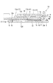
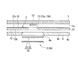
- FIG. 5 is an overall cross-sectional view of the illuminating device of FIG.
- FIG. 5 is an overall cross-sectional view of the lighting device of FIG. 1 and shows a cross section taken along line A2-A2 of FIG. It is sectional drawing which decomposes
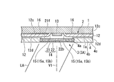
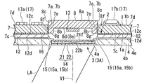
- FIG. 1 is a cross-sectional view showing the main part of the illumination device 10 according to the first embodiment of the present invention, and is a view showing a cross section (A1-A1 cross section) along the X direction in FIG.
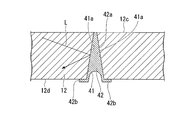
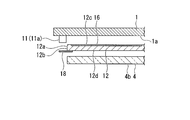
- FIG. 2 is a cross-sectional view illustrating an example of the groove 41 formed in the light guide 12 of the lighting device 10.
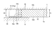
- FIG. 3 is a cross-sectional view illustrating another example of the groove 41 formed in the light guide 12 of the lighting device 10.
- FIG. 4 is a plan view of the illumination device 10.
- FIG. 5 is a cross-sectional view showing the second illumination unit 3 of the illumination device 10.
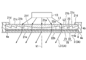
- FIG. 6 is a cross-sectional view showing the condensing element 21 and the photorefractive element 22 of the illumination device 10.
- FIG. 7 is an enlarged cross-sectional view showing the condensing element 21 and the photorefractive element 22.
- FIG. 8 is an overall cross-sectional view of the illuminating device 10 and is a view showing a cross section A1-A1 of FIG.
- FIG. 9 is an overall cross-sectional view of the illumination device 10, and is a view showing a cross section A2-A2 of FIG.
- FIG. 10 is an exploded cross-sectional view of the second illumination unit 3 of the illumination device 10, and is a cross-sectional view along the X direction of FIG. FIG.
- FIG. 11 is an exploded cross-sectional view of the first illumination unit 2 of the illumination device 10, and is a cross-sectional view along the Y direction of FIG.
- FIG. 12 is a cross-sectional view of the first lighting unit 2 of the lighting device 10.
- FIG. 13 is a cross-sectional view of an example of the substrate 1 that can be used in the lighting device 10.
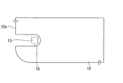
- FIG. 14 is a plan view of an example of the light guide 12 that can be used in the lighting device 10.
- FIG. 15 is a plan view of another example of the light guide 12 that can be used in the lighting device 10.
- the illumination device 10 includes a substrate 1, a first illumination unit 2 that emits first illumination light, and a second narrower range than the first illumination unit 2.
- a second illumination unit 3 that emits illumination light, a cover unit 4 that covers them, and a frame unit 5 to which the cover unit 4 is attached are provided.
- the illuminating device 10 can be installed, for example, on the ceiling of a vehicle and used as an interior lamp.
- the lighting device 10 can be installed in a vehicle by fixing the frame portion 5 to an interior material 6 of the vehicle, for example.
- the first illumination unit 2 includes a sheet-like light guide 12 installed along one surface 1 a (a lower surface or a surface, also referred to as a reference surface 1 a) of the substrate 1.
- the first light source 11 for introducing light into the light guide 12 is provided.
- the 1st illumination part 2 can be used as a room lamp which illuminates a wide range (for example, the whole vehicle interior).
- the first light source 11 is composed of one or a plurality of light sources 11 a mounted on one surface 1 a of the substrate 1.
- the first light source 11 includes a plurality of light sources 11 a, and these light sources 11 a are arranged along one end edge 12 a of the light guide 12.
- the one end edge portion 12a provided with the light source 11a in this example is one of the four side portions of the light guide 12 having a substantially rectangular shape in plan view, and more specifically, one end of the light guide 12 having a substantially rectangular shape. Long side.
- the light source 11a can be installed in a partial range including the central portion in the length direction of the one end edge portion 12a. The number and positions of the light sources 11a are determined so that the brightness of the first illumination light introduced into the light guide 12 and surface-emitted does not vary.
- the light source 11 a is installed with the light emitting surface 11 b facing the end surface 12 b of the one end edge portion 12 a of the light guide 12.
- a light emitting diode hereinafter referred to as LED
- the light emitting element used as the light source 11a is not limited to the LED but may be a cold cathode tube.
- the light guide 12 is made of a transparent light-transmitting resin.
- urethane resin acrylic resin, polycarbonate resin, silicone resin, polystyrene resin, polyimide resin, polymethyl methacrylate (PMMA) elastomer, urethane acrylate, or the like is used. it can.
- the thickness T1 of the light guide 12 is set equal to or greater than the height H1 of the light source 11a, the light introduction efficiency from the light source 11a can be increased, and the luminance and illuminance of the first illumination light can be increased. .
- the thickness T1 of the light guide 12 is preferably 0.5 mm or more (preferably 0.7 mm or more). Thereby, even when a high-brightness type large LED or the like that can cope with an increase in the area of the light guide 12 is used as the light source 11a, the utilization efficiency of light from the light source 11a can be increased. If the thickness of the light guide 12 is within the above range (0.5 mm or more), the height of the end surface 12b is sufficiently larger than the height of the light source 11a. This is because the incidence rate of light can be increased. Therefore, the luminance and illuminance can be increased, and the area of the light guide 12 can be increased. When the thickness T1 of the light guide 12 is 2 mm or less (preferably 1.5 mm or less), it is preferable in terms of reducing the thickness of the lighting device 10.
- the thickness T1 of the light guide 12 can be made substantially the same as the height H1 of the light source 11a. Although the thickness T1 and the height H1 may be different, the difference between the thickness T1 and the height H1 is preferably within ⁇ 0.3 mm. Thereby, the incidence rate of light from the light source 11a to the light guide 12 can be increased.
- a groove 41 that partitions the light guide 12 is formed on the lower surface 12 d of the light guide 12.
- the groove part 41 can be made into the shape where a width
- the cross-sectional shape of the groove part 41 is not restricted to this, A width
- the groove portion 41 can be formed so as to penetrate the light guide 12, or as shown in FIG. 3, can have a depth that does not reach the upper surface 12 c.
- the groove part 41 shown in FIG. 3 has a V-shaped cross section.
- the depth of the groove part 41 is not specifically limited, It is preferable to set it as 50% or more of the thickness of the light guide 12 from a viewpoint of the improvement of a reflectance.
- the width of the groove 41 can be set to 0.01 to 2 mm, for example.
- the groove part 41 should just be formed in the at least one surface of the light guide 12. FIG. That is, the groove 41 may be formed only on either the lower surface 12d or the upper surface 12c of the light guide 12, or may be formed on both the lower surface 12d and the upper surface 12c.
- the method for forming the groove 41 is not particularly limited, but laser processing or the like is suitable.
- the groove portion 41 shown in FIG. 2 has a groove-like structure formed by inner surfaces 41 a and 41 a of slits formed through the light guide 12 and the surface 1 a of the substrate 1.
- the formation position (formation position in plan view) of the groove portion 41 is such that the light guide 12 is divided into a plurality of regions.
- the groove 41 extends linearly in the Y direction from the positions near both ends of the formation range of the first light source 11 at the one end edge 12a and reaches the other end edge 12f.
- the pair of groove portions 41 partitions an inner region R1 (first region) sandwiched between them from outer regions R2 and R2 (second region).
- R1 first region sandwiched between them from outer regions R2 and R2 (second region).
- the X direction is a direction parallel to one end edge portion 12 a that is the long side of the substantially rectangular light guide 12
- the Y direction is a direction (short side direction) orthogonal to the X direction.
- a light reflective resin 42 containing light reflective fine particles exhibiting white color is embedded in the groove portion 41.
- the light reflecting fine particles contained in the light reflecting resin 42 for example, titanium oxide (TiO 2 ), calcium carbonate (CaCO 3 ) and the like can be used, and titanium oxide is particularly preferable.
- the light-reflecting fine particles function as a white pigment, and the light-reflecting resin 42 is white.
- the content of titanium oxide in the light-reflective resin 42 is preferably 5% by mass or more, particularly 5 to 50% by mass (preferably 10 to 40% by mass).
- the particle size of titanium oxide is preferably 10 nm to 0.5 ⁇ m.
- resin used for the light reflective resin 42 For example, an acrylic resin, a urethane resin, a vinyl acetate resin etc. can be used.
- the light reflective resin 42 is preferably embedded in the groove 41 so as to cover at least a part (preferably all) of the inner surface 41 a of the groove 41.
- the inner surface 41 a of the groove portion 41 is covered with the light reflective resin 42 over the entire surface.
- the light reflective resin 42 may be filled in the entire internal space of the groove 41, or may be filled only in a part of the internal space of the groove 41.
- the light-reflective resin 42 is embedded in the groove 41, leaving a space on the lower surface 12 d side, not the entire internal space of the groove 41.
- the light-reflecting resin 42 may be embedded only in the groove portion 41, but as shown in the example, a main body portion 42a that is in the light-reflecting resin 42 and covers the inner surface 41a of the groove portion 41, and a main body portion It is good also as a shape which has the extension part 42b extended outward along the lower surface 12d from 42a, and covering the lower surface 12d by predetermined width.
- the light L propagating in the inner region R ⁇ b> 1 (see FIG. 4) is internally reflected by the inner surface 41 a of the groove portion 41 by embedding the light reflecting resin 42 exhibiting white in the groove portion 41. Therefore, the light is reused in the inner region R1 and light leaked to the outer region R2 is suppressed.
- incident light is scattered on the upper surface 12 c (one surface or back surface) which is the surface of the light guide 12 on the substrate 1 side, and the lower surface 12 d (the other surface or surface) of the light guide 12 is scattered.
- the light extraction portion 16 can be formed in a part or all of the upper surface 12c.
- the light in the light guide 12 is extracted to the lower surface 12d side as surface light emission (first illumination light).
- the 1st illumination part 2 functions as a planar light-emitting device.
- the light extraction part 16 can emit light over the substantially entire area of the light guide 12 by being formed uniformly over the entire area of the upper surface 12c.
- the light extraction unit 16 can be a plurality of microdot-like ink layers (hereinafter simply referred to as microdots) formed by printing, for example.
- the planar view shape of the minute dots may be arbitrary, such as a circle, an ellipse, or a polygon (such as a rectangle).
- the minute dots can be formed by a printing method such as a screen printing method, a gravure printing method, or a pad printing method.
- the ink constituting the fine dots for example, white ink using titanium oxide as a pigment is suitable. Since titanium oxide functions as a white pigment, the ink exhibits a white color. When the titanium oxide content of the ink is 5 to 50% by mass or more, preferably 10 to 40% by mass or more, high luminance can be obtained. Examples of titanium oxide include rutile type and anatase type, and rutile type titanium oxide is particularly preferable. In order to emit white light, it is necessary to uniformly scatter the entire visible light. Here, considering the relationship between the wavelength to be scattered and the particle size of titanium oxide, the particle size of titanium oxide is preferably 10 nm to 0.5 ⁇ m.
- the light extraction portion is not limited to the ink layer, and may be a notch formed on the surface of the light guide, or a rough surface portion formed by sandblasting or the like.
- the other surface 1b (upper surface or back surface) of the substrate 1 is provided with an electronic component 17 (such as a semiconductor element) for turning on and off the light sources 11 and 13 and adjusting the amount of light. 17a to 17c) are implemented.
- an electronic component 17 such as a semiconductor element
- the electronic component 17 a publicly known one can be used.
- the substrate 1 is preferably provided with a touch pad 30 (detection sensor).
- the touch pad 30 includes an input sensor 31 and a resist layer 32 (covering resin layer) formed on one surface thereof.
- the input sensor 31 is a sensor that detects the proximity or contact of a detection target such as a human finger.
- the input sensor 31 is a capacitance type input sensor, and has a configuration in which the wiring layer 34 is provided on one surface of the base material 33. Since the capacitance type input sensor 31 has a simple structure including a single substrate 33 and a wiring layer 34, it can be thinned.
- the base material 33 is a plate material made of a resin such as PET.
- the base material 33 may be a flexible substrate made of PEN (polyethylene naphthalate), polyimide, or the like, or a rigid substrate made of glass epoxy resin or the like.
- the wiring layer 34 has, for example, a plurality of electrodes 34a.
- an object to be detected such as a human finger approaches, an electrostatic capacity is formed between the object to be detected and the electrode 34a, and this capacitance is determined by an opposing area or a separation distance between the object to be detected and the electrode 34a. It depends on. For this reason, the detected object and the electrode 34a form a variable capacitance section.
- a change in the capacitance of the variable capacitance unit is detected by a detection means (not shown), and an input operation by the detection target, its position, and the like are grasped by a control unit (not shown) based on the detected value.
- the wiring layer 34 can be formed, for example, by heating a silver paste containing silver particles after screen printing on the substrate 33.
- the wiring layer 34 may be formed by etching a copper foil laminated on the base material 33.
- the resist layer 32 secures electrical insulation between the wiring layers 34 and prevents oxidation, and the base material 33 and the wiring layer 34 are formed on one surface (surface on the light guide 12 side) side of the input sensor 31. It is formed to cover.
- a general-purpose solder resist can be used as the resist layer 32.
- the touch pad 30 When the touch pad 30 is used, for example, the user is detected and the light source is turned on or off, the light source is turned on or off when the user holds the hand, the light amount or irradiation position is moved by moving the hand. It is possible to use such as adjusting.
- the substrate 1 may be a printed wiring board such as a PCB (Printed Circuit Board) or an FPC (Flexible Printed Circuit).
- a touch pad 30 may be provided on the surface 1 b side of the substrate 1 separately from the substrate 1.
- the touch pad 30 employs a capacitance type input sensor 31.
- the input sensor another type, for example, a resistance film type input sensor may be employed.
- FIG. 37 shows an example of a touch pad using a resistance film type input sensor.
- the touch pad 160 (detection sensor) includes an upper substrate 161 having a transparent conductive film 163 formed on the opposing surface 161a, and an opposing surface. 162a and a lower substrate 162 on which a transparent conductive film 164 is formed. A plurality of dot spacers 166 are formed on the transparent conductive film 164 of the lower substrate 162.
- the upper substrate 161 and the lower substrate 162 are disposed so that the transparent conductive films 163 and 164 face each other with a space therebetween.
- a reflective layer 165 (reflector) is formed on the upper surface 161 b of the upper substrate 161.
- the reflective layer 165 functions as a reflector that reflects light leaked downward from the light guide 12.
- Reference numeral 167 denotes an adhesive layer.
- the touch pad 160 when pressed downward by an object to be detected (such as a user's finger), the upper substrate 161 bends downward, and the transparent conductive films 163 and 164 come into contact with each other to conduct electricity. Is detected.
- FIG. 38 shows a pressure-sensitive membrane switch 170.
- the membrane switch 170 includes an upper substrate 171 having a wiring layer 173 and an upper electrode 176 formed on the opposing surface 171a, and a wiring layer 174 and a lower portion on the opposing surface 172a. And a lower substrate 172 on which an electrode 177 is formed.
- the upper substrate 171 and the lower substrate 172 are arranged so that the electrodes 176 and 177 face each other with a space therebetween.
- a resist layer 175 (covering resin layer) is formed on the upper surface 171 b of the upper substrate 171.
- the resist layer 175 functions as a reflector that reflects light leaked downward from the light guide 12.
- Reference numeral 178 denotes an adhesive layer.
- the membrane switch 170 when the upper substrate 171 is bent downward by the pressure of the detection target (user's finger or the like), the upper electrode 176 contacts the lower electrode 177, and these are electrically connected to detect an input operation or the like.
- a mask 18 having a light shielding property can be provided on the lower surface side of the range including the first light source 11 and the one end edge 12 a of the light guide 12.
- the mask 18 in the illustrated example is formed from the first light source 11 to the one end edge 12 a of the light guide 12.
- the mask 18 is preferably made of a white material.
- the second illumination unit 3 includes a second light source 13 mounted on one surface 1a of the substrate 1 and light from the second light source 13 perpendicular to the substrate 1. And an optical path changing unit 14 as second illumination light in a direction inclined with respect to the direction V1.
- the 2nd illumination part 3 can be used as a map lamp (spot lamp) which selectively illuminates a narrow range (for example, a driver
- the second light source 13 is mounted on one surface 1 a of the substrate 1.
- two second light sources 13 are provided on the substrate 1 apart from each other.
- a light emitting diode (henceforth LED) (light emitting element) can be used.
- the light emitting element used as the second light source 13 may be a cold cathode tube.
- the number of the second light sources 13 is not limited to the illustrated example, and may be 1 or 3 or more.
- the light guide 12 is formed with an opening 15 that can accommodate the second light source 13.
- the shape of the opening 15 in plan view is not particularly limited, and may be a circle as shown in this figure, or may be another shape such as an ellipse or a rectangle.
- the opening 15 is not limited to a closed shape (see FIG. 14) surrounding the second light source 13, but may be an open shape reaching the edge 12e of the light guide 12 as shown in FIG.
- the opening 15 in this example is formed so as to gradually increase in diameter from the upper surface 12c toward the lower surface 12d. That is, the inner surface 15b of the peripheral edge portion 15a of the opening 15 is inclined so as to gradually move away from the second light source 13 from the upper surface 12c toward the lower surface 12d. In the opening 15, the light reflected by the inner surface 15 b of the peripheral edge 15 a travels downward, so that the amount of second illumination light increases.
- At least a part of the inner surface 15b of the peripheral edge portion 15a can be a reflecting surface that reflects light from the second light source 13.
- the entire inner surface 15b is preferably a reflective surface.
- the reflective surface of the inner surface 15b is preferably one that can efficiently reflect light from the second light source 13.
- the inner surface 15b can be made a reflective surface by using a paint (for example, mirror ink) containing metal powder.
- a metal thin film may be formed on the inner surface 15b by a known method.
- At least a part of the inner surface 15b of the peripheral edge portion 15a can also function as a light shielding surface that blocks light from the first light source 11. Thereby, it is possible to prevent light from the first light source 11 propagating through the light guide 12 from leaking from the inner surface 15b, and it is possible to prevent the light use efficiency from the first light source 11 from being lowered.
- the reflection surface that reflects the light from the second light source 13 also functions as a light shielding surface that blocks the light from the first light source 11.
- a reflecting surface is formed on the inner surface 15b, the light from the first light source 11 is also reflected in the light guide 12, and the utilization efficiency thereof can be increased.
- the optical path changing unit 14 includes a condensing element 21 that narrows the light emission range from the second light source 13 and a light refracting element 22 that refracts the light from the second light source 13.
- the condensing element 21 may be designed according to the spread angle of the light from the second light source 13 and the angle of the light required for the light emitted from the condensing element 21.
- a part of a curved surface such as a surface, a cylindrical surface, or an elliptical cylindrical surface may be a main shape, or a combination of a plurality of these curved surfaces may be used.
- the condensing element 21 in the illustrated example is a Fresnel lens in which a plurality of convex lenses are concentrically combined, and includes a central portion 21a and a first outer peripheral portion 21b formed on the outer peripheral side of the central portion 21a. And a second outer peripheral portion 21c formed on the outer peripheral side of the first outer peripheral portion 21b, and a third outer peripheral portion 21d formed on the outer peripheral side of the second outer peripheral portion 21c.
- the central portion 21a and the outer peripheral portions 21b to 21d are lenses having a curved surface on the lower surface 21e side.
- the outermost peripheral part of the second outer peripheral part 21c is thinner than the innermost peripheral part of the third outer peripheral part 21d
- the outermost peripheral part of the first outer peripheral part 21b is thinner than the innermost peripheral part of the second outer peripheral part 21c
- the outermost periphery is thinner than the innermost periphery of the first outer periphery 21b. Due to this structure, the condensing element 21 of this example is thinner than a normal convex lens.
- the upper surface 21f of the condensing element 21 is a flat surface along one surface 1a of the substrate 1 and is substantially parallel to the surface 1a (see FIG. 5). For this reason, the condensing element 21 is in a posture along the substrate 1.
- the condensing element 21 can collimate the light from the second light source 13.
- the emitted light L ⁇ b> 1 from the second light source 13 is converted into light L ⁇ b> 2 that is parallel light by the condensing element 21.
- the condensing element 21 is not necessarily parallelized as long as the light emission range from the second light source 13 can be sufficiently narrowed.
- the optical path changing unit 14 has a structure in which a photorefractive element 22 is provided on the lower surface side of the condensing element 21 (on the opposite side to the second light source 13 side).
- the photorefractive element 22 refracts light from the second light source 13 and directs it in a direction inclined with respect to the direction V ⁇ b> 1 perpendicular to the substrate 1.
- the second illumination unit 3 (3A) located on the left in FIG.
- the second illumination light LA tilted to the left with respect to the direction V1 is obtained by the photorefractive element 22, and the second illumination unit 3 (on the right) In 3B), the second refracting light LB tilted to the right with respect to the direction V1 is obtained by the photorefractive element 22.
- the angles (inclination angle ⁇ shown in FIG. 1) of the second illumination lights LA and LB with respect to the direction V1 perpendicular to the substrate 1 are, for example, 1 ° or more and 45 ° or less.
- the inclination angle of the second illumination light is, for example, an angle with respect to the direction V1 of the light traveling direction at the light flux center of the second illumination light.
- the second illumination lights LA and LB are inclined in the left-right direction.
- the inclination direction of the second illumination light is not limited to this, and the second illumination light is in a direction other than the illustrated direction.
- the photorefractive element 22 can also be installed so that the illumination light is inclined.
- the second illumination light may be inclined in a direction (front side or back side with respect to the paper surface) perpendicular to the paper surface in FIG.
- the photorefractive element 22 has one or more prism portions 23 that refract light.
- a plurality of prism portions 23 are formed continuously on the upper surface 22 a of the photorefractive element 22.
- One surface (inner peripheral surface 23a) (see FIG. 7) of the prism portion 23 is inclined with respect to the direction V1.
- the inclination direction of the inner peripheral surface 23a is determined according to the required inclination direction of the second illumination light LA.
- the inner peripheral surface 23a of the prism portion 23 of the second illumination unit 3 (3A) located on the left in FIG. 1 is inclined so as to descend to the right as shown in FIGS. Yes.
- the outer peripheral surface 23b of the prism portion 23 can be a surface along the direction V1.
- the lower surface 22b of the photorefractive element 22 is a flat surface along one surface 1a of the substrate 1 and is substantially parallel to the surface 1a (see FIG. 5). For this reason, the photorefractive element 22 is in a posture along the substrate 1.
- the condensing element 21 and the light refracting element 22 are fitted into the mounting opening 4a formed in the lower plate 4b of the cover 4 and the peripheral edge of the mounting opening 4a. Can be fixed to.
- the lower surface 22 b of the photorefractive element 22 is flush with the lower surface 4 e (the surface opposite to the second light source 13 side) of the lower plate portion 4 b of the cover portion 4.
- the lower surface 22b may be on the back side (above the lower surface 4e in FIGS. 5 and 6) with respect to the lower surface 4e of the lower plate portion 4b.
- the condensing element 21 and the photorefractive element 22 are installed in the attachment opening 4 a of the cover part 4, and thus do not protrude from the cover part 4. For this reason, the condensing element 21 and the photorefractive element 22 are not easily damaged by an external force.
- the positional relationship between the condensing element 21 and the light refracting element 22 is not limited to the illustrated example, and the condensing element 21 may be installed on the lower surface side of the light refracting element 22.
- the cover portion 4 covers and protects the substrate 1, the first illumination portion 2, and the second light source 13, and includes a flat plate-like lower plate portion 4 b and its peripheral edge. And a side plate portion 4c formed on the side plate.
- the cover portion 4 can be attached to the frame portion 5 by locking a locking claw portion 4d formed outward on the side plate portion 4c in the locking hole 5a of the frame portion 5.
- the cover portion 4 is preferably made of a transparent material that can transmit light, and is made of, for example, resin or glass.
- the illumination light obtained by the 1st illumination part 2 and the 2nd illumination part 3 of the illuminating device 10 is demonstrated.
- the first illumination unit 2 the light emitted from the first light source 11 (light source 11a) enters the light guide 12 from the end surface 12b of the one end edge 12a, The light propagates through the light guide 12 mainly toward the other end edge portion 12f (see FIGS. 4 and 9) while being reflected by the upper surface 12c, the lower surface 12d, and the like.
- a part of the light propagating in the light guide 12 is scattered by the light extraction unit 16 and extracted to the lower surface 12d side.
- the 1st illumination light which is planar light emission is obtained.
- the first illumination light illuminates a wide range (for example, the entire interior of the vehicle) where the illumination device 10 is installed. For this reason, the 1st illumination part 2 can be used as a room lamp.
- the light emitted from the first light source 11 is introduced into the inner region R1 of the light guide 12 and propagates in the inner region R1.
- the light L propagating in the inner region R ⁇ b> 1 is internally reflected by the inner surface 41 a of the groove 41, so that the light propagates again in the light guide 12 and can be reused. For this reason, the brightness
- region R1 can be raised.
- the light L is internally reflected by the inner surface 41a of the groove part 41, it is difficult for the light L to propagate to the outer region R2.
- region in the 1st illumination part 2, the target area
- the groove 41 is not noticeable, and is not easily restricted in appearance with respect to the position where the groove 41 is formed. Further, since a simple structure in which the light reflecting resin 42 is embedded in the groove portion 41 is adopted, it can be applied to the case where the thin light guide 12 is used, which is advantageous in terms of thinning the device and reducing the cost. Furthermore, compared with the case where the reflecting structure is formed on the end face of the light guide, the reflecting structure is hardly damaged by an external force, and the durability is excellent.
- the light L1 emitted from the second light source 13 is diffused light that spreads in the emission direction.
- the incident range is narrowed by entering the light collecting element 21.
- the light L2 transmitted through the condensing element 21 is parallel light.
- the light L2 is directed to the light refracting element 22, is incident on the inner peripheral surface 23a that is the inclined surface of the prism portion 23, is transmitted through the light refracting element 22, and is converted into light L3 from the lower surface 22b.
- the light L3 is directed in a direction inclined with respect to the direction V1.
- the second illumination light selectively illuminates a narrow range (for example, the hand of a driver or a passenger in the passenger seat) compared to the first illumination light.
- the 2nd illumination part 3 can be used as a map lamp (spot lamp).
- the optical path changing unit 14 of the second illuminating unit 3 includes the condensing element 21 and the light refracting element 22, so that light whose emission range is sufficiently narrowed by the condensing element 21 is supplied to the light refracting element 22. It can be made incident. For this reason, the 2nd illumination light inclined by sufficient angle is obtained. As a result, it is not necessary to place the condensing element 21 and the photorefractive element 22 in an inclined manner, so that the apparatus can be reduced in thickness and size. Moreover, since the condensing element 21 and the photorefractive element 22 can be set in a posture along the substrate 1, the apparatus can have a flat plate structure.
- both the first lighting unit 2 and the second lighting unit 3 are provided on one substrate 1 and the light guide 12 is also provided along the substrate 1, a plurality of substrates is required. Compared with the case where an inclined arrangement of a light guide or the like is required, the apparatus configuration is simple, and from this point, it is suitable for thinning and miniaturization.
- the illumination device 10 can be manufactured by a simple procedure of providing the light guide 12, the light sources 11, 13 and the like on the one surface 1a side of the substrate 1 on which the electronic component 17 is mounted in advance. There is also an advantage that the cost can be reduced.
- the second illumination unit 3 is provided on the substrate 1, even when a high-power second light source 13 is used, the heat generated by the light source 13 is dispersed throughout the substrate 1 to prevent a local temperature rise and stable. Can be secured.
- both the first illuminating unit 2 and the second illuminating unit 3 are provided on one substrate 1, even when a high output light source 11 or 13 is used, the heat generated by the light sources 11 and 13 is generated on the substrate 1. It can be dispersed throughout to prevent local temperature rise and ensure stable operation.
- the condensing element 21 and the photorefractive element 22 may be inclined with respect to the substrate 1 in a direction corresponding to the second illumination light as long as the thinning and downsizing of the illumination device 10 can be achieved. .
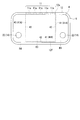
- FIG. 16 is a plan view of a lighting apparatus according to the second embodiment of the present invention.
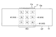
- the groove portion 41 is a pair of main portions 41A that linearly extend in the Y direction from positions near both ends of the first light source 11 forming range of the one end edge portion 12a toward the other end edge portion 12f. , 41A and a connecting portion 41B that connects the end portions on the other end edge portion 12f side of the main portions 41A, 41A.
- a light reflective resin 42 is embedded in the groove 41.
- the connecting portion 41B is formed along the other end edge portion 12f at a position away from the other end edge portion 12f by a predetermined distance.
- it can be set as the same as the illuminating device 10 of 1st Embodiment shown in FIG.
- the inner region R3 (first region) surrounded by the main portions 41A and 41A and the connecting portion 41B can be partitioned from another region (outer region R4) to increase the brightness. Since the groove part 41 has the connection part 41B, high brightness can be achieved even in the vicinity of the connection part 41B far from the first light source 11.
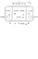
- FIG. 17 is a plan view of a lighting apparatus according to the third embodiment of the present invention.
- the groove part 41 is formed along the peripheral edge part of the light guide 12 from the vicinity of the both ends of the formation range of the 1st light source 11 of the one end edge part 12a.
- the groove portion 41 is formed on the entire peripheral edge portion of the light guide body 12 excluding the formation range of the first light source 11 so as to be separated from the peripheral edge portion by a predetermined distance.
- a light reflective resin 42 is embedded in the groove 41.
- it can be set as the same as the illuminating device 10 of 1st Embodiment shown in FIG.
- the inner region R5 (first region) surrounded by the groove 41 can be partitioned from other regions (outer region R6) (second region) to increase the brightness. Since the inner region R5 is a wide region covering almost the entire region of the light guide 12, the light emitting region of the first illumination light can be enlarged.
- FIG. 18 is a plan view of a lighting device according to the fourth embodiment of the present invention.
- a plurality of light sources 11a constituting the first light source 11 are arranged side by side in a range over almost the entire length of the one end edge portion 12a of the light guide 12, and therefore, the first light source shown in FIG. It differs from the illuminating device 10 of embodiment.
- a light reflective resin 42 is embedded in the groove 41.
- the light from the first light source 11 can be introduced not only into the inner region R1 but also into the outer region R2, and the first illumination light can be obtained from the outer region R2.
- FIG. 19 is a plan view of a lighting apparatus according to the fifth embodiment of the present invention.
- This embodiment is different from the second embodiment in that the grooves are formed in multiples.
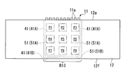
- a second groove portion 51 having a rectangular frame shape is formed along the groove portion 41 at a predetermined distance from the first groove portion 41 inside the first groove portion 41. That is, the groove part is formed in double.
- the second groove 51 has a main portion 51A, 51A formed at a constant distance from the main portion 41A, 41A inside the main portion 41A, 41A, and a constant portion from the connecting portion 41B inside the connecting portion 41B.
- the connecting portion 51B is formed at a distance.
- the second groove 51 can be formed by laser processing or the like, and a light reflective resin 42 is embedded in the second groove 51.
- the inner region R7 (first region) of the second groove 51 can be partitioned from other regions (outer region R8) to increase the brightness.
- the effect of preventing leakage light from the inner region R7 to the outer region R8 is enhanced by the double-structured groove portions 41 and 51, and the inner region R8 can be further increased in luminance.
- a groove part is good also as a multiple structure of 3 or more.
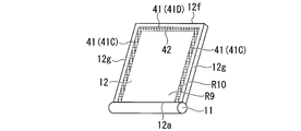
- FIG. 20 is a perspective view schematically showing the first illumination unit of the illumination apparatus according to the sixth embodiment of the present invention.
- the groove portion 41 has a pair of main portions 41C and 41C extending linearly along the side edge portions 12g and 12g from the positions close to both ends of the one end edge portion 12a toward the other end edge portion 12f. And a connecting portion 41D for connecting the end portions on the other end edge portion 12f side of the main portions 41C and 41C.
- a light reflective resin 42 is embedded in the groove 41.
- the inner region R9 (first region) surrounded by the main portions 41C, 41C and the connecting portion 41D is partitioned from other regions (outer region R10) (second region) to increase the brightness. it can.
- FIG. 21 is a perspective view schematically showing a first illumination unit of the illumination apparatus according to the seventh embodiment of the present invention.
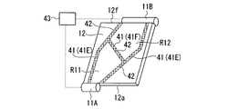
- the first illumination unit shown here includes the light guide 12, one end side light source 11 ⁇ / b> A provided at one end edge 12 a of the light guide 12, and the other end provided at the other end edge 12 f of the light guide 12.
- a side light source 11B and a control unit 43 that independently controls turning on and off of the light sources 11A and 11B are provided.
- the groove portion 41 includes a pair of main portions 41E and 41E formed from the one end edge portion 12a to the other end edge portion 12f, and a connecting portion 41F that connects intermediate portions in the length direction of the main portions 41E and 41E. It consists of.
- the region between the main portions 41E and 41E is connected to one end side region R11 (first region) on the one end edge 12a side and the other end side region R12 (second region) on the other end edge 12f side by the connecting portion 41F. It is divided into.
- a light reflective resin 42 is embedded in the groove 41.
- the one end side light source 11A is installed at a position where light can be introduced into the one end side region R11
- the other end side light source 11B is installed at a position where light can be introduced into the other end side region R12.
- the one end side region R11 and the other end side region R12 can be partitioned from other regions to increase the brightness, and the controller 43 independently turns on and off the one end side light source 11A and the other end side light source 11B. By controlling the light emission, the light emission in the one end side region R11 and the other end side region R12 can be individually adjusted.
- the two light sources 11A and 11B are employed, but the number of light sources is not limited to this, and may be any number of three or more. Further, the number of regions partitioned by the groove is not limited to 2, and can be any number of 3 or more. When the number of light sources and regions is three or more, one of the plurality of light sources can introduce light into one region, and one of the other light sources can emit light into one of the other regions. It is possible to adopt a configuration that makes it possible to introduce.
- FIG. 22 is a perspective view schematically showing a first illumination unit of the illumination apparatus according to the eighth embodiment of the present invention.
- the groove portion 41 includes a base portion 41G along the one end edge portion 12a, and extending portions 41H and 41H extending in a direction intersecting the base portion 41G while being separated from each other toward the one end edge portion 12a. It is the shape which has.
- a light reflective resin 42 is embedded in the groove 41.
- One or more grooves 41 may be formed. In this embodiment, the brightness of the inner region of the groove 41 can be increased. Since there is no restriction
- FIG. 23 is a plan view schematically showing the first illumination unit of the illumination apparatus according to the ninth embodiment of the present invention.
- FIG. 24 is a cross-sectional view schematically illustrating an illumination device including the first illumination unit.
- this lighting device is an electronic device such as a mobile phone, a personal digital assistant (PDA), a personal computer, and the like, and includes a first lighting unit 2 and a light guide body 12 of the first lighting unit 2.
- a sheet switch 61 provided on the lower surface 12d side of the light guide and a key mat (not shown) provided on the upper surface 12c side of the light guide 12 are provided.
- the sheet switch 61 includes a plurality of center contact portions 63, an annular contact portion 65 that surrounds each center contact portion 63, and a dome-shaped metal that covers each contact portion 63, 65 on the upper surface 62 a (one surface) of the substrate 62.
- a plate 64 is provided. The metal plate 64 is deformed downward by pressing the operation key of the key mat and is brought into contact with the central contact portion 63 so that the central contact portion 63 and the annular contact portion 65 can be electrically connected.
- the central contact portion 63, the annular contact portion 65 surrounding the central contact portion 63, and the metal plate 64 constitute a pressure-sensitive switch element 66.
- the 1st illumination part 2 is provided with the light guide 12 and the 1st light source 11 which introduces light into this.
- a light extraction portion 16 is formed in the light guide 12 in an area 19 (hereinafter referred to as a key area 19) corresponding to the operation keys of the key mat.
- a groove portion 41 is formed on the upper surface 12 c of the light guide 12 in the vicinity of one or a plurality of key regions 19 that are relatively far from the first light source 11.
- the groove portion 41 is formed in a substantially L shape along two side portions that are far from the first light source 11 among the four side portions of the substantially rectangular key region 19.
- a light reflective resin 42 is embedded in the groove 41.
- the groove portion 41 includes a first extending portion 41J formed along the lower side 19a with a predetermined distance downward from the lower side 19a of the key area 19, and a left side with a predetermined distance leftward from the left side 19b of the key area 19. It is made into the substantially L shape which consists of the 2nd extension part 41K formed along 19b.
- the extended portions 41J and 41K of the groove portion 41 are formed close to the key region 19 along the sides 19a and 19b far from the first light source 11, they are incident on the light guide 12 from the first light source 11.
- the light propagating in the surface direction of the light guide 12 is internally reflected by the groove portion 41, and the key region 19 can be increased in luminance.
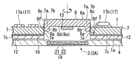
- FIG. 29 is an overall cross-sectional view of the illumination device 110 according to the tenth embodiment of the present invention.
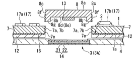
- the substrate 1 is provided with a concave structure 8 having a concave portion 8d.
- a second light source 13 is provided in the concave portion 8 d of the concave structure 8.
- the substrate 1 includes a plate-like substrate body 7 in which the attachment opening 7a is formed, and a concave structure 8 attached to the substrate body 7 by closing the attachment opening 7a.
- the shape of the mounting opening 7a in plan view is preferably circular. Note that the shape of the attachment opening 7a may be a rectangle, a polygon, or the like.
- the attachment opening 7 can be formed in a place (empty space) on the substrate 1 where the electronic component 17 and the wiring need not be provided.
- the concave structure 8 can be made into the shape which has the top-plate part 8a and the side-plate part 8b extended from the peripheral part 8c.
- the top plate portion 8a can be formed in a flat plate shape.
- the plan view shape of the top plate portion 8a can be a shape corresponding to the mounting opening portion 7a of the substrate body 7, for example, a circle, a rectangle, or the like.
- a second light source 13 is provided on the lower surface 8e of the top plate portion 8a.
- the plan view shape of the side plate portion 8b can be a shape corresponding to the mounting opening portion 7a of the substrate body 7, for example, a circle, a rectangle, or the like.
- the side plate portion 8b in the illustrated example has a shape (for example, a cylindrical shape, a rectangular tube shape, or the like) that extends downward (or substantially perpendicular) to the top plate portion 8a.
- the side plate portion 8b may have other shapes, for example, a shape (skirt shape) that becomes wider in the extending direction.
- the concave structure 8 is not limited to the illustrated shape (covered cylindrical shape), and may have another shape, for example, a hemispherical shape or a conical shape.
- the concave structure 8 in the illustrated example is formed to protrude upward from the other surface 1b of the substrate 1 (the surface opposite to the reference surface 1a. Specifically, the other surface 7d (upper surface or back surface) of the substrate body 7). However, since the mounting opening 7 is formed at a location where the electronic component 17 or the like does not need to be provided, the mounting of the electronic component 17 is not hindered.
- the concave portion 8d of the concave structure 8 (the top plate portion 8a and the side plate portion 8b).
- the cylindrical space on the inner surface side is formed to be recessed from the reference surface 1a of the substrate 1 (specifically, one surface 7c (lower surface or surface) of the substrate body 7) toward the surface 1b.
- the second light source 13 is provided on the inner surface of the concave portion 8d (specifically, the lower surface 8e of the top plate portion 8a), the second light source 13 is separated from the optical path changing unit 14 as compared with the case where it is installed on one surface 7c of the substrate body 7. Can be installed in position. For this reason, the distance between the second light source 13 and the optical path changing unit 14 can be sufficiently secured without increasing the thickness dimension of the illumination device 110.
- the optical path changing unit 14 In order for the optical path changing unit 14 to obtain good optical path changing characteristics, a predetermined distance is required between the second light source 13 and the optical path changing unit 14. Since the illuminating device 110 has the concave portion 8d, the distance between the second light source 13 and the optical path changing portion 14 can be arbitrarily determined by setting the height position of the top plate portion 8a. Therefore, this distance can be optimized according to the optical characteristics of the optical path changing unit 14, and second illumination light having good characteristics can be obtained.
- the concave structure 8 can have a shape protruding upward from the other surface 1 b (7 d) of the substrate 1, the height position of the inner surface of the concave portion 8 d is limited within the thickness range of the substrate 1. Rather, it is possible to secure a sufficient distance between the second light source 13 and the optical path changing unit 14.
- the concave structure 8 is formed so as to protrude upward from the surface 1b (7d) of the substrate 1, but the concave structure 8 is not limited to this and is formed from the surface 1b of the substrate 1.
- a configuration that does not protrude that is, a configuration in which the upper surface of the concave structure 8 is flush with the surface 1b (7d) of the substrate 1 may be employed.
- a wiring formed on the other surface 1b (7d) of the substrate 1 or a wiring that can be electrically connected to the electronic component 17 can be formed on the concave structure 8. As a result, power supply to the second light source 13 and control of turning on and off the second light source 13 can be performed.
- At least a part of the inner surface of the concave portion 8d of the concave structure 8 can be a reflective surface that reflects light from the second light source 13.
- the entire inner surface of the concave portion 8d is preferably a reflective surface.
- the reflective surface is preferably one that can efficiently reflect light from the second light source 13.
- the inner surface of the concave portion 8d can be made a reflecting surface by applying a paint containing metal powder (for example, mirror ink).
- the configuration of the reflecting surface is not limited to this, and the reflecting surface can also be formed by a metal thin film formed on the inner surface of the concave portion 8d by a known method.
- At least a part of the inner surface of the recessed portion 8d of the recessed structure 8 may be a light absorbing surface that absorbs light from the second light source 13.
- a method of forming a light absorption layer is possible.
- the light absorption layer is not particularly limited as long as it has a function of absorbing light.
- a layer made of a coloring material can be employed.
- the color of the coloring material is preferably dark in terms of light absorption function, and particularly black.
- the coloring material layer can be formed of a material containing a black pigment such as carbon black.
- the concave structure 8 can be separated from the substrate body 7.
- the side plate portion 8b of the concave structure 8 is disposed in the attachment opening 7a, so that the concave structure 8 is attached to the substrate body 7 with the attachment opening 7a closed (see FIG. 30A). ).
- the concave structure 8 has a structure that can be detachably attached to the peripheral edge portion 7b of the attachment port portion 7a.
- the mounting structure is preferably a screw fitting structure that can be freely fitted and removed.
- a male screw portion 8f is formed on the outer surface of the cylindrical side plate portion 8b, and a female screw portion 7e that is screwed into the male screw portion 8f is formed on the inner surface of the peripheral edge portion 7b.
- the male threaded portion 8f and the female threaded portion 7e can be attached to and detached from the peripheral edge portion 7b by screw fitting.
- the concave structure 8 can adjust the height position (position in the thickness direction of the substrate 1) according to the fitting state of the male screw portion 8f and the female screw portion 7e.
- the concave structure 8 In the state shown in FIG. 30A, the concave structure 8 is completely screwed into the mounting opening 7a, the lower end 8g of the side plate 8b reaches the same height as the surface 1a (7c) of the substrate 1, and the concave structure 8 and the second light source 13 are in a relatively low position.
- the concave structure 8 is adjusted by adjusting the fitting state between the male screw portion 8 f and the female screw portion 7 e by rotating it around the axis in the winding direction or in the opposite direction.
- the height can be set arbitrarily.
- the male screw portion 8f of the concave structure 8 is screwed slightly shallowly with respect to the female screw portion 7e, and the concave structure 8 is at a position slightly higher than the position shown in FIG. 30A.
- the recessed structure 8 can set the height position with respect to the board
- the concavo-convex engagement structure which can be engaged / disengaged can also be provided in the side-plate part 8b and the peripheral part 7b.
- the concave structure 8 is formed by forming a locking projection on the outer surface of the side plate 8b and forming a locking recess on the inner surface of the peripheral edge 7b that can be detachably engaged with the locking projection. It can be made detachable with respect to the peripheral part 7b.
- the concave structure 8 may be formed integrally with the substrate body 7.
- the concave structure 8 is provided in a portion where there is no electronic component 17 or the like (empty space), the structure in the cover portion 4 (the substrate 1, the first illumination portion 2, the second illumination portion). 3) and the like is not increased, so that there is no problem in reducing the thickness of the lighting device 110.
- the base material 1 (substrate body 7) is not particularly limited, but for example, a plate material formed of a resin such as PET can be used.
- the substrate 1 may be a rigid substrate made of glass epoxy resin or the like.
- the light guide 12 is formed with an opening 15 having the same shape as the mounting opening 7 a of the substrate body 7.
- the opening 15 can also be formed so as to surround the attachment opening 7a and have a diameter larger than that of the attachment opening 7a.
- At least a part of the inner surface 15b of the peripheral edge 15a can be a reflecting surface that reflects light from the second light source 13 by applying a mirror ink or forming a metal thin film.
- At least a part of the inner surface 15 b can also function as a light blocking surface that blocks light from the first light source 11.
- the concave portion 8d is formed on the reference surface 1a (7c) of the substrate 1, and the second light source 13 is provided in the concave portion 8d. Therefore, the structure in the cover portion 4 (substrate 1, first) Without increasing the thickness dimension of the illumination unit 2, the second illumination unit 3, etc.), a sufficient distance between the second light source 13 and the optical path changing unit 14 can be secured to obtain the second illumination light having good characteristics. be able to. Therefore, the lighting device 110 can be thinned.
- the illuminating device 110 can secure a sufficient distance between the second light source 13 and the optical path changing unit 14 without causing the optical path changing unit 14 to protrude from the cover unit 4 to the front side of the apparatus (the lower side in FIG. 29). Therefore, the surface of the lighting device 110 can be formed flat. Therefore, it is preferable in terms of ease of operation, aesthetics, ease of manufacture, and the like. As shown in FIG. 29, a space having a height capable of accommodating the electronic component 17 and the like is secured in the lighting device 110 on the surface 1b side of the substrate 1 opposite to the reference surface 1a.
- the concave structure 8 protrudes upward from the surface 1b, if the concave structure 8 is provided in a portion where there is no electronic component 17 or the like (empty space), the structure (substrate 1, 1 illuminating unit 2, second illuminating unit 3, etc.) are not increased in thickness, and there is no problem in thinning the apparatus.
- FIG. 31 is a cross-sectional view showing a part of a lighting apparatus according to the eleventh embodiment of the present invention.
- a concave structure portion 119 is formed on a part of the substrate 1.
- the concave structure portion 119 has a shape having a top plate portion 119a and a side plate portion 119b extending from the peripheral edge portion 119c, and is formed integrally with the substrate 1.
- the top plate portion 119a can be formed in a flat plate shape.
- the plan view shape of the top plate portion 119a can be, for example, a circle or a rectangle.
- the second light source 13 is provided on the lower surface 119e of the top plate portion 119a.
- the side plate portion 119b can have a shape (skirt shape) that gradually increases in width in the extending direction.
- the side plate portion 119b may have a shape that extends downward (or substantially perpendicular) to the top plate portion 119a.
- the concave structure portion 119 may not protrude from the other surface 1b (7d) of the substrate 1, and the upper surface of the concave structure body 119 may be flush with the surface 1b.
- the inner surface of the concave portion 119d of the concave structure portion 119 (the frustoconical space on the inner surface side of the top plate portion 119a and the side plate portion 119b) is formed to be recessed from the reference surface 1a of the substrate 1 toward the surface 1b side. Since the second light source 13 is provided on the inner surface of the concave portion 119d (specifically, the lower surface 119e of the top plate portion 119a), the second light source 13, the optical path changing unit 14, and the like without increasing the thickness dimension of the illumination device. Can be secured sufficiently. Since the distance between the second light source 13 and the optical path changing unit 14 can be arbitrarily determined by setting the height position of the top plate part 119a, this distance is optimized according to the optical characteristics of the optical path changing unit 14, The second illumination light having good characteristics can be obtained.
- At least a part of the inner surface of the concave portion 119d (the inner surface of the top plate portion 119a and the side plate portion 119b) of the concave structure portion 119 is a reflective surface that reflects light from the second light source 13 by applying a mirror ink or forming a metal thin film. can do.
- the concave portion 119d as a reflecting surface, the light from the second light source 13 can be efficiently directed to the optical path changing unit 14 and the light use efficiency can be increased.
- At least a part of the inner surface of the concave portion 119d of the concave structure 119 may be a light absorption surface that absorbs light from the second light source 13 by forming a light absorption layer such as the above-described coloring material layer.
- the manufacturing is easier and the manufacturing cost can be reduced as compared with the case where the concave structure body 8 separate from the substrate body 7 is used. There are advantages.
- FIG. 32 is a cross-sectional view showing a part of a lighting apparatus according to the twelfth embodiment of the present invention.
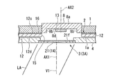
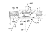
- the optical path changing unit 14 includes a condensing element 21 that is a Fresnel lens.
- the position of the optical axis AX1 of the condensing element 21 is shifted from the position of the optical axis AX2 of the second light source 13.
- the optical axis AX2 is a line along the traveling direction of light at the center of the light beam emitted from the second light source 13, and passes through the center of the second light source 13 and is perpendicular to the reference plane 1a of the substrate 1 in the illustrated example.
- the optical axis AX1 is a line along the central axis of the condensing element 21 and is perpendicular to the reference plane 1a of the substrate 1.
- the positional deviation of the optical axes AX1 and AX2 is an in-plane positional deviation along the reference plane 1a of the substrate 1.
- the direction of deviation of the optical axis AX1 of the condensing element 21 with respect to the optical axis AX2 of the second light source 13 is a direction corresponding to the inclination direction of the second illumination light.
- the optical axis AX1 of the condensing element 21 is on the left side of the optical axis AX2 of the second light source 13, and thereby, in the direction V1 perpendicular to the substrate 1
- the second illumination light LA inclined leftward is obtained.
- FIG. 33 is a cross-sectional view showing a part of a lighting apparatus according to a thirteenth embodiment of the present invention.
- the optical path changing unit 14 includes a condensing element 21A that is a convex lens whose upper surface 21g is a convex curved surface.
- the condensing element 21A may be designed according to the spread angle of the light from the second light source 13 and the inclination angle of the light required for the light emitted from the condensing element 21A.
- a part of a curved surface such as an object surface, a cylindrical surface, or an elliptical cylindrical surface may be a main shape, or a shape obtained by combining a plurality of these curved surfaces.
- the condensing element 21A may be in a posture in which the curved surface 21g faces downward and the flat surface 21h faces upward.
- the light condensing element 21 ⁇ / b> A may be a convex lens whose upper and lower surfaces are convex curved surfaces.
- the position of the optical axis AX1 of the condensing element 21A is shifted from the position of the optical axis AX2 of the second light source 13.
- the optical axis AX2 is a line along the traveling direction of light at the center of the light beam emitted from the second light source 13, and passes through the center of the second light source 13 and is perpendicular to the reference plane 1a of the substrate 1 in the illustrated example.
- the optical axis AX1 is, for example, a line along the central axis of the light condensing element 21A, and is perpendicular to the one surface 1a of the substrate 1.
- the positional deviation of the optical axes AX1 and AX2 is an in-plane positional deviation along the reference plane 1a of the substrate 1.
- the direction of deviation of the optical axis AX1 of the condensing element 21A with respect to the optical axis AX2 of the second light source 13 is a direction corresponding to the inclination direction of the second illumination light.
- the optical axis AX1 of the light condensing element 21A is on the left side of the optical axis AX2 of the second light source 13, and thereby, in the direction V1 perpendicular to the substrate 1
- the second illumination light LA inclined leftward is obtained.
- the light guide 112 shown here is formed with a thick portion 113 that gradually increases in thickness toward the one end edge 112a facing the light source 11a.
- the thick portion 113 of the illustrated example has an inclined surface 113a that descends toward the lower surface 112d as it approaches the one end edge portion 112a.
- the upper surface 112c side of the thick portion 113 is a flat surface along the reference surface 1a.
- An inclination angle ( ⁇ in FIG. 34) of the inclined surface 113a with respect to the reference surface 1a may be, for example, 1 to 20 degrees.
- the thickness of the thick portion 113 at the one end edge portion 112a is preferably 0.5 mm or more.
- the thickness of the thick part 113 in the one end edge part 112a can be 2 mm or less.
- the thick portion 113 can be formed extending in the depth direction of FIG.
- the incidence rate when the light from the light source 11a enters the light guide 112 from the end surface 112b of the one end edge portion 112a can be increased, and the light utilization efficiency can be increased. Since the light guide 112 can be formed thin except for the thick portion 113, the space inside the apparatus can be saved.
- the thick portion may have an inclined surface on the upper surface 112c side.
- the thick portion 114 shown here has an inclined surface 114a that rises toward the top surface 112c as it approaches the one end edge portion 112a.
- the lower surface 112d side of the thick portion 114 is a flat surface along the reference surface 1a.
- the inclination angle of the inclined surface 114a may be the same as that of the inclined surface 113a in FIG.
- a height adjusting unit 115 is formed on a part of the substrate 1.
- the height adjustment unit 115 includes an adjustment unit main part 115a and an inclined part 115b extending from the edge thereof.
- the lower surface of the inclined portion 115b is an inclined surface 115c that descends as the distance from the adjusting portion main portion 115a increases.
- the inclined surface 114a of the thick portion 114 is formed on the inclined surface 115c of the inclined portion 115b. Even in this example, the use efficiency of light can be increased by forming the thick portion 114. In addition, since portions other than the thick portion 114 can be formed thin, space saving inside the apparatus can be achieved.
- the reflecting member for example, a plate material formed of a resin such as white PET can be used.
- a film made of silver or the like may be formed on the surface of the reflecting member in order to increase reflection efficiency.
- the low refractive index layer can be formed on one or both surfaces of the light guide.
- the low refractive index layer is a layer made of a material having a refractive index lower than that of the light guide, and for example, a fluororesin can be used.
- the refractive index of the low refractive index layer is preferably as low as possible, and can be, for example, 1.4 or less (for example, 1 to 1.4).
- the thickness of the low refractive index layer can be, for example, 0.01 to 0.03 mm.
- Example 1 The test apparatus shown in FIG. 25 is arranged along the one end edge 12a at the central portion of one end edge 12a of the light guide 12 (length 180 mm, width 65 mm, thickness 1.3 mm) formed on the substrate.
- the light source 11 which consists of 10 LED11a (20 mA per one) was provided.
- a rectangular frame-shaped groove 41 is formed which includes a connecting portion 41B that connects ends of the main portions 41A and 41A on the other end edge portion 12f side.
- the groove part 41 was formed by penetrating the light guide 12 by laser processing, and the width thereof was 0.5 mm.
- a light reflective resin 42 (white ink) containing titanium oxide (light reflective fine particles) (20 mass%) was embedded in the groove 41 (see FIG. 2).
- the distance between the main portions 41A and 41A of the groove portion 41 is 60 mm, and the distance between the one end edge portion 12a and the connecting portion 41B is 60 mm.
- Light from the first light source 11 is introduced into the rectangular introduction region R13 surrounded by the groove 41.
- FIG. 25 shows the measurement results of luminance at the nine measurement points (first measurement point P1 to ninth measurement point P9) in the introduction region R13.
- the position where the numerical value is written corresponds to the position of each measurement point P1 to P9 (see FIG. 25). For example, the three numerical values in the lower part of the “brightness at first to ninth points” column in FIG.
- FIG. 27 are the luminances at measurement points P7 to P9 from the left.
- FIG. 27 shows the measurement results of the luminance of the entire introduction region R13 and the luminance non-uniformity.
- FIG. 28 shows the result of measuring the illuminance at a position away from the horizontally installed light guide 12 by a predetermined distance (30 to 90 cm) in the height direction.
- a second groove 51 is formed along the groove 41 inside the groove 41. That is, the groove part is formed in double.
- the second groove 51 includes main portions 51A and 51A formed at a predetermined distance (1 mm) from the main portions 41A and 41A inside the main portions 41A and 41A, and a connecting portion 41B inside the connecting portion 41B. Is formed in a rectangular frame shape including a connecting portion 51 ⁇ / b> B formed at a certain distance (1 mm).
- the width of the groove 51 is the same as the width of the groove 41.
- the distance between the main parts 51A and 51A of the groove 51 is 60 mm
- the distance between the one end edge 12a and the connecting part 51B is 60 mm
- the introduction region R13 surrounded by the groove 51 and the one end 12a is an example. It is the same size as one introduction region R13.
- Other configurations of the test apparatus are the same as those in the first embodiment. Using this test apparatus, luminance and the like were measured. The results are also shown in FIG. The measurement result of illuminance is shown in FIG.
- Example 1 A test apparatus having a light guide 12 (length 180 mm, width 60 mm, thickness 1.3 mm) in which no groove was formed was prepared.
- the size of the introduction region R13 of this test apparatus is the same as the introduction region R13 of the first embodiment.
- Other configurations of the test apparatus are the same as those in the first embodiment.
- luminance and the like were measured. The results are also shown in FIG. The measurement result of illuminance is shown in FIG.
- the light in the light guide 12 is internally reflected by the grooves 41 and 51 and reused.
- the luminance in R13 particularly the luminance at measurement points P7 to P9 far from the light source 11, could be increased.
- the luminance at the measurement points (for example, the measurement points P7 to P9) far from the light source 11 can be increased.
- the luminance non-uniformity in the introduction region R13 is reduced. That is, the luminance of the introduction region R13 can be made uniform.
- the brightness of the measurement points (for example, the measurement points P7 to P9) far from the light source 11 is higher.
- the overall brightness was increased and the brightness was made uniform. From FIG. 28, it can be seen that in Examples 1 and 2 in which the groove portions were formed, a high value was obtained for illuminance, and in particular, in Example 2 in which the two groove portions 41 and 51 were formed, high illuminance was obtained.
- Substrate 1a One side of substrate (reference plane) 2 1st illumination part 3 2nd illumination part 4 Cover part 7 Substrate body 7a Attachment port part 7b Peripheral part 8 Concave structure 8d, 119d Concave part 11 1st light source 11A One end side light source 11B The other end side light source 12, 112 Light guide Body 13 Second light source 14 Optical path changing unit 21 Condensing element 22 Photorefractive element 25 Positioning member 30 Touch pad (detection sensor) 41 Groove part 42 Light reflective resin 43 Control part R1, R3, R5, R7, R9 Inner area
Landscapes
- Engineering & Computer Science (AREA)
- General Engineering & Computer Science (AREA)
- Mechanical Engineering (AREA)
- Physics & Mathematics (AREA)
- General Physics & Mathematics (AREA)
- Optics & Photonics (AREA)
- Planar Illumination Modules (AREA)
- Arrangement Of Elements, Cooling, Sealing, Or The Like Of Lighting Devices (AREA)
- Arrangements Of Lighting Devices For Vehicle Interiors, Mounting And Supporting Thereof, Circuits Therefore (AREA)
Abstract
光源と、光源からの光が導入されて面方向に導かれるシート状の導光体とを備えた面状発光装置。導光体の下面には、導光体内の光を内部反射する溝部が形成され、溝部内部の少なくとも一部に、白色を呈する光反射性微粒子を含む光反射性樹脂が埋め込まれている。
Description
本発明は、車両の室内灯、電子機器、液晶表示装置などに使用できる面状発光装置および照明装置に関する。
本願は、2011年3月28日に、日本に出願された特願2011-70808号に基づき優先権を主張し、その内容をここに援用する。
本願は、2011年3月28日に、日本に出願された特願2011-70808号に基づき優先権を主張し、その内容をここに援用する。
車両の室内灯、電子機器(携帯電話等)、液晶表示装置などには、照明機能を有する面状発光装置が用いられている。
この種の面状発光装置としては、光源と、この光源からの光が導入される導光板とを備え、この導光板の側端面の一部を着色して側端面で光が反射可能としたものがある(例えば、特許文献1参照)。この構造の面状発光装置は、導光板の側端面から光が漏れるのを防ぎ、それによって光源から離れた箇所での輝度を高め、全体として輝度の均一化を図ることができる。
この種の面状発光装置としては、光源と、この光源からの光が導入される導光板とを備え、この導光板の側端面の一部を着色して側端面で光が反射可能としたものがある(例えば、特許文献1参照)。この構造の面状発光装置は、導光板の側端面から光が漏れるのを防ぎ、それによって光源から離れた箇所での輝度を高め、全体として輝度の均一化を図ることができる。
しかしながら、前記面状発光装置では、組立時や製品の使用時に端面の着色部が破損し、その効果が低くなることがあった。
また、着色部は導光板の端面に設けられるため、効果が得られる範囲や大きさが導光板の外形による制限を受けることから、導光板の形状等によっては十分な輝度向上効果が得られないことがあった。
本発明は、上記事情に鑑みてなされたものであり、設計の自由度が高く、任意の箇所の輝度を調整できる面状発光装置および照明装置を提供することを目的とする。
また、着色部は導光板の端面に設けられるため、効果が得られる範囲や大きさが導光板の外形による制限を受けることから、導光板の形状等によっては十分な輝度向上効果が得られないことがあった。
本発明は、上記事情に鑑みてなされたものであり、設計の自由度が高く、任意の箇所の輝度を調整できる面状発光装置および照明装置を提供することを目的とする。
上記課題を解決するために、本発明では以下の構成を提供する。
本発明は、1または複数の光源と、前記光源からの光が導入されて面方向に導かれるシート状の導光体とを備え、前記導光体の少なくとも一方の面には、前記導光体内の光を内部反射する溝部が少なくとも1つ形成され、前記溝部の内部の少なくとも一部に、白色を呈する光反射性微粒子を含む光反射性樹脂が埋め込まれている面状発光装置を提供する。
前記溝部は、前記導光体の一部である第1領域を囲んで、その外の第2領域から区画する構成とすることができる。
本発明の面状発光装置は、前記複数の光源の点灯および消灯を独立的に制御する制御部をさらに備え、前記複数の光源のうち1つは、前記第1領域に光を導入可能であり、それ以外の光源のうち1つは、前記第2領域に光を導入可能である構成とすることができる。
前記溝部は、前記導光体を貫通して形成されている構成とすることができる。
前記光反射性微粒子は、酸化チタンからなることが好ましい。
本発明は、1または複数の光源と、前記光源からの光が導入されて面方向に導かれるシート状の導光体とを備え、前記導光体の少なくとも一方の面には、前記導光体内の光を内部反射する溝部が少なくとも1つ形成され、前記溝部の内部の少なくとも一部に、白色を呈する光反射性微粒子を含む光反射性樹脂が埋め込まれている面状発光装置を提供する。
前記溝部は、前記導光体の一部である第1領域を囲んで、その外の第2領域から区画する構成とすることができる。
本発明の面状発光装置は、前記複数の光源の点灯および消灯を独立的に制御する制御部をさらに備え、前記複数の光源のうち1つは、前記第1領域に光を導入可能であり、それ以外の光源のうち1つは、前記第2領域に光を導入可能である構成とすることができる。
前記溝部は、前記導光体を貫通して形成されている構成とすることができる。
前記光反射性微粒子は、酸化チタンからなることが好ましい。
本発明は、前記面状発光装置を有する第1照明部と、基板と、前記第1照明部よりも狭い範囲に第2照明光を発する第2照明部と、を備え、前記第1照明部が、前記基板の一方の面に沿うシート状の導光体と、前記導光体に光を導入し面方向に伝搬させて前記第1照明光を得る第1光源とを有し、前記第2照明部が、前記基板の一方の面に実装された第2光源と、前記第2光源からの光を前記基板に垂直な方向に対し傾斜した方向に向けて前記第2照明光とする光路変更部とを有し、前記導光体の少なくとも一方の面には、前記導光体内の光を内部反射する溝部が少なくとも1つ形成され、前記溝部の内部の少なくとも一部に、白色を呈する光反射性微粒子を含む光反射性樹脂が埋め込まれている照明装置を提供する。
本発明は、前記導光体が形成された前記基板の基準面に、前記基準面とは反対面側に向けて凹む凹状部が形成され、前記第2光源は、前記凹状部内に設けられている構造を採用できる。
本発明は、前記基板が、取付口部を有する基板本体と、前記凹状部を有する凹状構造体とを備え、前記凹状構造体が、前記取付口部の周縁部に着脱自在に取付け可能である構造を採用できる。
前記凹状構造体は、前記取付口部の周縁部にネジ嵌合により取付け可能であり、ネジ嵌合の状態に応じて前記基板の厚さ方向の位置を調整できることが好ましい。
前記凹状部は、前記基板に一体に形成された凹状構造部の内面であってもよい。
前記凹状部の内面の少なくとも一部は、前記第2光源からの光を反射する反射面とされていてもよい。
前記凹状部の内面の少なくとも一部は、前記第2光源からの光を吸収する光吸収面とされていてもよい。
前記光路変更部は、前記光の出射範囲を狭める集光素子と、前記光を屈折させて前記基板に垂直な方向に対し傾斜した方向に向ける光屈折素子とを有し、前記集光素子と光屈折素子は、前記基板に沿う姿勢とされていることが好ましい。
本発明は、前記導光体が形成された前記基板の基準面に、前記基準面とは反対面側に向けて凹む凹状部が形成され、前記第2光源は、前記凹状部内に設けられている構造を採用できる。
本発明は、前記基板が、取付口部を有する基板本体と、前記凹状部を有する凹状構造体とを備え、前記凹状構造体が、前記取付口部の周縁部に着脱自在に取付け可能である構造を採用できる。
前記凹状構造体は、前記取付口部の周縁部にネジ嵌合により取付け可能であり、ネジ嵌合の状態に応じて前記基板の厚さ方向の位置を調整できることが好ましい。
前記凹状部は、前記基板に一体に形成された凹状構造部の内面であってもよい。
前記凹状部の内面の少なくとも一部は、前記第2光源からの光を反射する反射面とされていてもよい。
前記凹状部の内面の少なくとも一部は、前記第2光源からの光を吸収する光吸収面とされていてもよい。
前記光路変更部は、前記光の出射範囲を狭める集光素子と、前記光を屈折させて前記基板に垂直な方向に対し傾斜した方向に向ける光屈折素子とを有し、前記集光素子と光屈折素子は、前記基板に沿う姿勢とされていることが好ましい。
本発明によれば、導光体に、光反射性樹脂を埋め込んだ溝部が形成されているので、導光体内を伝搬する光は溝部の内面で内部反射し、再度導光体内に光が伝播し光を再利用できる。従って、目的とする領域の輝度を高めることができる。
導光体の少なくとも一方の面に、導光体を区画する溝部を少なくとも1つ設けるので、溝部形成位置は、導光体の形状による制限を受けないことから、自由度の高い光学設計が可能となる。従って、組立てや加工の容易性を損なうことなく、光学的な特性向上が可能である。
また、白色を呈する光反射性微粒子を含む光反射性樹脂を用いるため、光反射性樹脂による光の吸収が起こりにくく、光の利用効率を高めることができる。
溝部は、光反射性樹脂が白色であるため目立ちにくく、溝部の形成位置についての外観上の制約が生じにくいため、設計の自由度の点で優れている。
本発明は、溝部に光反射性樹脂が埋め込まれた簡単な構造を採用するため、薄い導光体を用いる場合にも適用でき、装置の薄型化や低コスト化の点で有利である。
さらに、導光体の端面に反射構造を形成する場合に比べ、外力による反射構造の破損が生じにくく、耐久性にも優れている。
導光体の少なくとも一方の面に、導光体を区画する溝部を少なくとも1つ設けるので、溝部形成位置は、導光体の形状による制限を受けないことから、自由度の高い光学設計が可能となる。従って、組立てや加工の容易性を損なうことなく、光学的な特性向上が可能である。
また、白色を呈する光反射性微粒子を含む光反射性樹脂を用いるため、光反射性樹脂による光の吸収が起こりにくく、光の利用効率を高めることができる。
溝部は、光反射性樹脂が白色であるため目立ちにくく、溝部の形成位置についての外観上の制約が生じにくいため、設計の自由度の点で優れている。
本発明は、溝部に光反射性樹脂が埋め込まれた簡単な構造を採用するため、薄い導光体を用いる場合にも適用でき、装置の薄型化や低コスト化の点で有利である。
さらに、導光体の端面に反射構造を形成する場合に比べ、外力による反射構造の破損が生じにくく、耐久性にも優れている。
以下、好適な実施の形態に基づき、図面を参照して本発明を説明する。
(第1の実施形態)
図1は、本発明の第1の実施形態である照明装置10の主要部を示す断面図であり、図4のX方向に沿う断面(A1-A1断面)を示す図である。図2は、照明装置10の導光体12に形成された溝部41の一例を示す断面図である。図3は、照明装置10の導光体12に形成された溝部41の他の例を示す断面図である。図4は、照明装置10の平面図である。図5は、照明装置10の第2照明部3を示す断面図である。図6は、照明装置10の集光素子21と光屈折素子22を示す断面図である。図7は、集光素子21と光屈折素子22を示す拡大断面図である。図8は、照明装置10の全体断面図であり、図4のA1-A1断面を示す図である。図9は、照明装置10の全体断面図であり、図4のA2-A2断面を示す図である。図10は、照明装置10の第2照明部3を分解して示す断面図であり、図4のX方向に沿う断面図である。図11は、照明装置10の第1照明部2を分解して示す断面図であり、図4のY方向に沿う断面図である。図12は、照明装置10の第1照明部2の断面図である。図13は、照明装置10に使用できる基板1の一例の断面図である。図14は、照明装置10に使用できる導光体12の一例の平面図である。図15は、照明装置10に使用できる導光体12の他の例の平面図である。
(第1の実施形態)
図1は、本発明の第1の実施形態である照明装置10の主要部を示す断面図であり、図4のX方向に沿う断面(A1-A1断面)を示す図である。図2は、照明装置10の導光体12に形成された溝部41の一例を示す断面図である。図3は、照明装置10の導光体12に形成された溝部41の他の例を示す断面図である。図4は、照明装置10の平面図である。図5は、照明装置10の第2照明部3を示す断面図である。図6は、照明装置10の集光素子21と光屈折素子22を示す断面図である。図7は、集光素子21と光屈折素子22を示す拡大断面図である。図8は、照明装置10の全体断面図であり、図4のA1-A1断面を示す図である。図9は、照明装置10の全体断面図であり、図4のA2-A2断面を示す図である。図10は、照明装置10の第2照明部3を分解して示す断面図であり、図4のX方向に沿う断面図である。図11は、照明装置10の第1照明部2を分解して示す断面図であり、図4のY方向に沿う断面図である。図12は、照明装置10の第1照明部2の断面図である。図13は、照明装置10に使用できる基板1の一例の断面図である。図14は、照明装置10に使用できる導光体12の一例の平面図である。図15は、照明装置10に使用できる導光体12の他の例の平面図である。
図1、図4、図8および図9に示すように、照明装置10は、基板1と、第1照明光を発する第1照明部2と、第1照明部2よりも狭い範囲に第2照明光を発する第2照明部3と、これらを覆うカバー部4と、カバー部4が取り付けられるフレーム部5とを備えている。
照明装置10は、例えば車両の天井部に設置して、室内灯として使用できる。図8および図9に示すように、照明装置10は、例えばフレーム部5を車両の内装材6に固定することで車両内に設置できる。
照明装置10は、例えば車両の天井部に設置して、室内灯として使用できる。図8および図9に示すように、照明装置10は、例えばフレーム部5を車両の内装材6に固定することで車両内に設置できる。
図4および図9に示すように、第1照明部2は、基板1の一方の面1a(下面または表面。基準面1aともいう。)に沿って設置されたシート状の導光体12と、導光体12に光を導入する第1光源11とを備えている。第1照明部2は、広い範囲(例えば車内全体)を照明するルームランプとして使用できる。
第1光源11は、基板1の一方の面1aに実装された1または複数の光源11aからなる。この例では、図4に示すように、第1光源11は複数の光源11aからなり、これら光源11aは、導光体12の一端縁部12aに沿って並べられている。
この例の光源11aが設けられた一端縁部12aは、平面視略矩形の導光体12の4つの辺部のうち1つであり、詳細には、略長方形の導光体12の一方の長辺である。光源11aは、一端縁部12aの長さ方向の中央部を含む一部範囲に設置することができる。光源11aの設置数および位置は、導光体12内に導入して面発光させた第1照明光の明るさに不均一が生じることがないように定められる。
この例の光源11aが設けられた一端縁部12aは、平面視略矩形の導光体12の4つの辺部のうち1つであり、詳細には、略長方形の導光体12の一方の長辺である。光源11aは、一端縁部12aの長さ方向の中央部を含む一部範囲に設置することができる。光源11aの設置数および位置は、導光体12内に導入して面発光させた第1照明光の明るさに不均一が生じることがないように定められる。
図11および図12に示すように、光源11aは、発光面11bを導光体12の一端縁部12aの端面12bに対面させて設置される。
光源11aとしては、発光ダイオード(以下、LEDという)(発光素子)を使用できる。なお、光源11aとして使用される発光素子は、LEDに限らず、冷陰極管などでもよい。
光源11aとしては、発光ダイオード(以下、LEDという)(発光素子)を使用できる。なお、光源11aとして使用される発光素子は、LEDに限らず、冷陰極管などでもよい。
導光体12は、透明な光透過性樹脂からなり、例えばウレタン樹脂、アクリル樹脂、ポリカーボネート樹脂、シリコーン樹脂、ポリスチレン樹脂、ポリイミド樹脂、ポリメチルメタクリレート(PMMA)のエラストマー、ウレタンアクリレート等を用いることができる。
導光体12の厚さT1は、光源11aの高さH1と同じ、またはこれより大きく設定すると、光源11aからの光の導入効率を高め、第1照明光の輝度および照度を高めることができる。
導光体12の厚さT1は、0.5mm以上(好ましくは0.7mm以上)が好ましい。
これによって、導光体12の大面積化に対応できる高輝度タイプの大型LED等を光源11aとして使用する場合でも、光源11aからの光の利用効率を高めることができる。導光体12の厚さを上記範囲(0.5mm以上)とすると、端面12bの高さが光源11aの高さ寸法に対して十分に大きくなるため、端面12bから導光体12内への光の入射率を高くできるからである。従って、輝度および照度を高めることができ、導光体12の大面積化を実現できる。
導光体12の厚さT1は、2mm以下(好ましくは1.5mm以下)とすると、照明装置10の薄型化の点で好ましい。
これによって、導光体12の大面積化に対応できる高輝度タイプの大型LED等を光源11aとして使用する場合でも、光源11aからの光の利用効率を高めることができる。導光体12の厚さを上記範囲(0.5mm以上)とすると、端面12bの高さが光源11aの高さ寸法に対して十分に大きくなるため、端面12bから導光体12内への光の入射率を高くできるからである。従って、輝度および照度を高めることができ、導光体12の大面積化を実現できる。
導光体12の厚さT1は、2mm以下(好ましくは1.5mm以下)とすると、照明装置10の薄型化の点で好ましい。
導光体12の厚さT1は、光源11aの高さH1とほぼ同じとすることができる。
厚さT1と高さH1は異なっていてもよいが、厚さT1と高さH1との差は±0.3mm以内であることが好ましい。これによって、光源11aから導光体12への光の入射率を高めることができる。
厚さT1と高さH1は異なっていてもよいが、厚さT1と高さH1との差は±0.3mm以内であることが好ましい。これによって、光源11aから導光体12への光の入射率を高めることができる。
図1および図2に示すように、導光体12の下面12dには、導光体12を区画する溝部41が形成されている。
溝部41は、深さ方向(図2の上方)に向けて徐々に幅が狭くなる形状とすることができる。なお、溝部41の断面形状はこれに限らず、深さ方向に幅が一定であってもよいし、深さ方向に幅広となる形状であってもよい。
溝部41は、例えば図2に示すように、導光体12を貫通して形成することもできるし、図3に示すように、上面12cに達しない深さとすることもできる。図3に示す溝部41は、断面V字形となっている。溝部41の深さは特に限定されないが、反射率の向上の観点から例えば導光体12の厚さの50%以上とすることが好ましい。
溝部41の幅は、例えば0.01~2mmとすることができる。
溝部41は、導光体12の少なくとも一方の面に形成されていればよい。すなわち、溝部41は、導光体12の下面12dおよび上面12cのいずれか一方にのみ形成されていてもよいし、下面12dと上面12cの両方に形成されていてもよい。
溝部41の形成方法は、特に限定されないが、レーザー加工などが好適である。
図2に示す溝部41は、導光体12を貫通して形成されたスリットの内面41a,41aと、基板1の面1aとで形成された溝状の構造を有する。
溝部41は、深さ方向(図2の上方)に向けて徐々に幅が狭くなる形状とすることができる。なお、溝部41の断面形状はこれに限らず、深さ方向に幅が一定であってもよいし、深さ方向に幅広となる形状であってもよい。
溝部41は、例えば図2に示すように、導光体12を貫通して形成することもできるし、図3に示すように、上面12cに達しない深さとすることもできる。図3に示す溝部41は、断面V字形となっている。溝部41の深さは特に限定されないが、反射率の向上の観点から例えば導光体12の厚さの50%以上とすることが好ましい。
溝部41の幅は、例えば0.01~2mmとすることができる。
溝部41は、導光体12の少なくとも一方の面に形成されていればよい。すなわち、溝部41は、導光体12の下面12dおよび上面12cのいずれか一方にのみ形成されていてもよいし、下面12dと上面12cの両方に形成されていてもよい。
溝部41の形成方法は、特に限定されないが、レーザー加工などが好適である。
図2に示す溝部41は、導光体12を貫通して形成されたスリットの内面41a,41aと、基板1の面1aとで形成された溝状の構造を有する。
図4に示すように、溝部41の形成位置(平面視における形成位置)は、導光体12を複数領域に区画するようにされる。
この例では、溝部41は、一端縁部12aにおける第1光源11の形成範囲の両端の近傍位置からそれぞれY方向に直線的に延出して他端縁部12fに達している。これら一対の溝部41は、これらに挟まれた内側領域R1(第1領域)を、外側領域R2、R2(第2領域)から区画している。
溝部41の形成位置には特に制限はなく、導光体12の任意の位置に形成することができる。
なお、図4において、X方向は、略長方形の導光体12の長辺である一端縁部12aに平行な方向であり、Y方向はX方向に直交する方向(短辺方向)である。
この例では、溝部41は、一端縁部12aにおける第1光源11の形成範囲の両端の近傍位置からそれぞれY方向に直線的に延出して他端縁部12fに達している。これら一対の溝部41は、これらに挟まれた内側領域R1(第1領域)を、外側領域R2、R2(第2領域)から区画している。
溝部41の形成位置には特に制限はなく、導光体12の任意の位置に形成することができる。
なお、図4において、X方向は、略長方形の導光体12の長辺である一端縁部12aに平行な方向であり、Y方向はX方向に直交する方向(短辺方向)である。
図2および図3に示すように、溝部41の内部には、白色を呈する光反射性微粒子を含む光反射性樹脂42が埋め込まれている。
光反射性樹脂42に含まれる光反射性微粒子としては、例えば酸化チタン(TiO2)、炭酸カルシウム(CaCO3)等が使用できるが、特に酸化チタンが好ましい。
光反射性微粒子は白色顔料として機能し、光反射性樹脂42は白色を呈する。酸化チタンを用いる場合の光反射性樹脂42中の酸化チタン含有率は、5質量%以上、特に5~50質量%(好ましくは10~40質量%)が好適である。
光反射性樹脂42に含まれる光反射性微粒子としては、例えば酸化チタン(TiO2)、炭酸カルシウム(CaCO3)等が使用できるが、特に酸化チタンが好ましい。
光反射性微粒子は白色顔料として機能し、光反射性樹脂42は白色を呈する。酸化チタンを用いる場合の光反射性樹脂42中の酸化チタン含有率は、5質量%以上、特に5~50質量%(好ましくは10~40質量%)が好適である。
白色の反射光を得るには可視光全域を散乱させる必要がある。散乱させる波長と、酸化チタンの粒径の関係を考慮すると、酸化チタンの粒径は10nm~0.5μmが好ましい。
光反射性樹脂42に用いられる樹脂としては、特に限定されないが、例えばアクリル樹脂、ウレタン樹脂、酢酸ビニル樹脂等が使用できる。
光反射性樹脂42に用いられる樹脂としては、特に限定されないが、例えばアクリル樹脂、ウレタン樹脂、酢酸ビニル樹脂等が使用できる。
光反射性樹脂42は、溝部41の内面41aの少なくとも一部(好ましくは全部)を覆うように溝部41に埋め込まれることが好ましい。図2および図3に示す例では、溝部41の内面41aは全面にわたって光反射性樹脂42に覆われている。光反射性樹脂42が内面41aに接することによって、内面41aでの反射効率が高められる。
光反射性樹脂42は、溝部41の内部空間全体に充填されていてもよいが、溝部41の内部空間の一部のみに充填されていてもよい。図示例では、光反射性樹脂42は、溝部41の内部空間全体ではなく、下面12d側に空間を残して溝部41に埋め込まれている。
光反射性樹脂42は、溝部41の内部にのみ埋め込まれていてもよいが、図示例のように、光反射性樹脂42内にあって溝部41の内面41aを覆う本体部42aと、本体部42aから下面12dに沿って外方に延出して下面12dを所定幅で覆う延出部42bとを有する形状としてもよい。
光反射性樹脂42は、溝部41の内部空間全体に充填されていてもよいが、溝部41の内部空間の一部のみに充填されていてもよい。図示例では、光反射性樹脂42は、溝部41の内部空間全体ではなく、下面12d側に空間を残して溝部41に埋め込まれている。
光反射性樹脂42は、溝部41の内部にのみ埋め込まれていてもよいが、図示例のように、光反射性樹脂42内にあって溝部41の内面41aを覆う本体部42aと、本体部42aから下面12dに沿って外方に延出して下面12dを所定幅で覆う延出部42bとを有する形状としてもよい。
図2および図3に示すように、白色を呈する光反射性樹脂42を溝部41に埋め込むことによって、内側領域R1(図4参照)内を伝搬する光Lは、溝部41の内面41aで内部反射するため、内側領域R1で再利用されるとともに、外側領域R2への漏れ光が抑えられる。
図12に示すように、導光体12の基板1側の面である上面12c(一方の面または裏面)には、入射光を散乱させて導光体12の下面12d(他方の面または表面)側に取り出す(出射させる)光取出部16を形成することができる。光取出部16は、上面12cの一部または全部の領域に形成することができる。光取出部16が広い範囲に形成されることによって、導光体12内の光は、面的な発光(第1照明光)として下面12d側に取り出される。第1照明部2は、面状発光装置として機能する。
光取出部16は、上面12cのほぼ全域にわたって均一に形成することによって、導光体12のほぼ全域を面的に発光させることができる。
光取出部16は、上面12cのほぼ全域にわたって均一に形成することによって、導光体12のほぼ全域を面的に発光させることができる。
光取出部16は、例えば印刷により形成された複数の微小ドット状のインク層(以下、単に微小ドットという)とすることができる。微小ドットの平面視形状は円形、楕円形、多角形(矩形等)など任意としてよい。微小ドットはスクリーン印刷法、グラビア印刷法、パッド印刷法などの印刷法により形成することができる。
微小ドットを構成するインクとしては、例えば顔料として酸化チタンを用いた白色インクが好適である。酸化チタンは白色顔料として機能するため、前記インクは白色を呈する。インクの酸化チタン含有率は、5~50質量%以上、好ましくは10~40質量%以上とすると高輝度が得られる。
酸化チタンとしては、ルチル型、アナターゼ型等があり、特に、ルチル型の酸化チタンが好ましい。
白色光を発光させるためには可視光全域を満遍なく散乱させる必要がある。ここで、散乱させる波長と、酸化チタンの粒径の関係を考慮すると、酸化チタンの粒径は10nm~0.5μmが望ましい。
なお、光取出部はインク層に限らず、導光体表面に形成された切り欠きでもよいし、サンドブラスト等によって形成した粗面部などであってもよい。
酸化チタンとしては、ルチル型、アナターゼ型等があり、特に、ルチル型の酸化チタンが好ましい。
白色光を発光させるためには可視光全域を満遍なく散乱させる必要がある。ここで、散乱させる波長と、酸化チタンの粒径の関係を考慮すると、酸化チタンの粒径は10nm~0.5μmが望ましい。
なお、光取出部はインク層に限らず、導光体表面に形成された切り欠きでもよいし、サンドブラスト等によって形成した粗面部などであってもよい。
図8および図9に示すように、基板1の他方の面1b(上面または裏面)には、例えば光源11、13の点灯、消灯、光量調整などを行うための半導体素子などの電子部品17(17a~17c)が実装されている。電子部品17としては、公知のものを使用できる。
図13に示すように、基板1としては、タッチパッド30(検知センサ)を備えたものが好適である。タッチパッド30は、入力センサ31と、その一方の面に形成されたレジスト層32(被覆樹脂層)とを備えている。
入力センサ31は、人間の手指等の被検出体の近接または接触を検出するセンサである。ここでは、入力センサ31は静電容量式の入力センサであって、基材33の一方の面に配線層34が設けられた構成である。静電容量式の入力センサ31は、1枚の基材33と配線層34からなる単純な構造であるため、薄型化が可能である。
入力センサ31は、人間の手指等の被検出体の近接または接触を検出するセンサである。ここでは、入力センサ31は静電容量式の入力センサであって、基材33の一方の面に配線層34が設けられた構成である。静電容量式の入力センサ31は、1枚の基材33と配線層34からなる単純な構造であるため、薄型化が可能である。
基材33は、例えばPETなどの樹脂で形成された板材である。基材33は、PEN(ポリエチレンナフタレート)、ポリイミド等からなるフレキシブル基板や、ガラスエポキシ樹脂等からなるリジッド基板であってもよい。
配線層34は、例えば複数の電極34aを有する。人間の手指等の被検出体が近づくと、被検出体と電極34aとの間には静電容量が形成され、この静電容量は被検出体と電極34aとの間の対向面積や離間距離によって変化する。このため、被検出体と電極34aは可変容量部を形成する。
可変容量部の静電容量の変化は検出手段(図示略)で検出され、その検出値に基づいて制御部(図示略)で被検出体による入力操作、その位置等が把握される。
可変容量部の静電容量の変化は検出手段(図示略)で検出され、その検出値に基づいて制御部(図示略)で被検出体による入力操作、その位置等が把握される。
配線層34は、例えば、銀粒子を含む銀ペーストを基材33上にスクリーン印刷した後に加熱することで形成することができる。配線層34は、基材33に積層した銅箔をエッチングすることにより形成してもよい。
レジスト層32は、配線層34間の電気絶縁性を確保するとともに酸化を防止するもので、入力センサ31の一方の面(導光体12側の面)側に、基材33および配線層34を覆って形成される。レジスト層32としては、例えば汎用のソルダレジストを使用できる。
レジスト層32は、配線層34間の電気絶縁性を確保するとともに酸化を防止するもので、入力センサ31の一方の面(導光体12側の面)側に、基材33および配線層34を覆って形成される。レジスト層32としては、例えば汎用のソルダレジストを使用できる。
タッチパッド30を用いる場合には、例えば利用者を検知して光源を点灯または消灯させる、利用者が手をかざすことで光源を点灯または消灯させる、かざした手を移動させることで光量または照射位置を調整する、などの使用方法が可能となる。
なお、基板1は、例えばPCB(Printed Circuit Board)、FPC(Flexible Printed Circuit)などのプリント配線基板であってもよい。
本発明では、基板1とは別に、基板1の面1b側にタッチパッド30(図13参照)を設けてもよい。
本発明では、基板1とは別に、基板1の面1b側にタッチパッド30(図13参照)を設けてもよい。
また、タッチパッド30(図13参照)では、静電容量式の入力センサ31が採用されているが、入力センサとしては、他の方式、例えば抵抗膜式の入力センサを採用してもよい。
図37は、抵抗膜式入力センサを用いたタッチパッドの一例を示すもので、このタッチパッド160(検知センサ)は、対向面161aに透明導電膜163が形成された上部基板161と、対向面162aに透明導電膜164が形成された下部基板162とを備えている。
下部基板162の透明導電膜164上には複数のドットスペーサ166が形成されている。上部基板161と下部基板162は、透明導電膜163、164が間隔をおいて向かい合うように配置される。
上部基板161の上面161bには、反射層165(反射体)が形成されている。反射層165は、導光体12から下方に漏れた光を反射させる反射体として機能する。反射層165には前記白色材料を使用すると、導光体12から漏れた光を反射させる効果を高めることができる。符号167は粘着層である。
タッチパッド160では、被検出体(使用者の手指等)によって下方に押圧されることにより、上部基板161が下方に撓み、透明導電膜163、164同士が接触して導通がなされ、入力操作等が検出される。
図37は、抵抗膜式入力センサを用いたタッチパッドの一例を示すもので、このタッチパッド160(検知センサ)は、対向面161aに透明導電膜163が形成された上部基板161と、対向面162aに透明導電膜164が形成された下部基板162とを備えている。
下部基板162の透明導電膜164上には複数のドットスペーサ166が形成されている。上部基板161と下部基板162は、透明導電膜163、164が間隔をおいて向かい合うように配置される。
上部基板161の上面161bには、反射層165(反射体)が形成されている。反射層165は、導光体12から下方に漏れた光を反射させる反射体として機能する。反射層165には前記白色材料を使用すると、導光体12から漏れた光を反射させる効果を高めることができる。符号167は粘着層である。
タッチパッド160では、被検出体(使用者の手指等)によって下方に押圧されることにより、上部基板161が下方に撓み、透明導電膜163、164同士が接触して導通がなされ、入力操作等が検出される。
本発明では、タッチパッド30に代えて、感圧式のメンブレンスイッチ(検知センサ)を使用することもできる。
図38は、感圧式のメンブレンスイッチ170を示すもので、このメンブレンスイッチ170は、対向面171aに配線層173および上部電極176が形成された上部基板171と、対向面172aに配線層174および下部電極177が形成された下部基板172とを備えている。
上部基板171と下部基板172は、電極176、177が間隔をおいて向かい合うように配置される。
上部基板171の上面171bにはレジスト層175(被覆樹脂層)が形成されている。レジスト層175は、導光体12から下方に漏れた光を反射させる反射体として機能する。レジスト層175に前記白色材料を使用すると、導光体12から漏れた光を反射させる効果を高めることができる。符号178は粘着層である。
このメンブレンスイッチ170では、被検出体(使用者の手指等)による押圧によって上部基板171が下方に撓むと、上部電極176が下部電極177に当接し、これらが導通して入力操作等が検出される。
図38は、感圧式のメンブレンスイッチ170を示すもので、このメンブレンスイッチ170は、対向面171aに配線層173および上部電極176が形成された上部基板171と、対向面172aに配線層174および下部電極177が形成された下部基板172とを備えている。
上部基板171と下部基板172は、電極176、177が間隔をおいて向かい合うように配置される。
上部基板171の上面171bにはレジスト層175(被覆樹脂層)が形成されている。レジスト層175は、導光体12から下方に漏れた光を反射させる反射体として機能する。レジスト層175に前記白色材料を使用すると、導光体12から漏れた光を反射させる効果を高めることができる。符号178は粘着層である。
このメンブレンスイッチ170では、被検出体(使用者の手指等)による押圧によって上部基板171が下方に撓むと、上部電極176が下部電極177に当接し、これらが導通して入力操作等が検出される。
図9、図11および図12に示すように、第1光源11および導光体12の一端縁部12aを含む範囲の下面側には、遮光性を有するマスク18を設けることができる。図示例のマスク18は、第1光源11から導光体12の一端縁部12aにかけて形成されている。マスク18には、白色材料を使用するのが好ましい。
マスク18を設けることによって、第1光源11からの光が外部に漏れるのを防ぎ、前記光の導光体12への導入効率を高めることができる。また、第1光源11およびその近傍における輝度が局所的に高くなるのを防ぐことができる。
マスク18を設けることによって、第1光源11からの光が外部に漏れるのを防ぎ、前記光の導光体12への導入効率を高めることができる。また、第1光源11およびその近傍における輝度が局所的に高くなるのを防ぐことができる。
図1、図5~図8に示すように、第2照明部3は、基板1の一方の面1aに実装された第2光源13と、第2光源13からの光を基板1に垂直な方向V1に対し傾斜した方向に向けて第2照明光とする光路変更部14とを有する。
第2照明部3は、狭い範囲(例えば運転者や助手席の同乗者の手元)を選択的に照明するマップランプ(スポットランプ)として使用できる。
第2照明部3は、狭い範囲(例えば運転者や助手席の同乗者の手元)を選択的に照明するマップランプ(スポットランプ)として使用できる。
図1、図5、図8および図10に示すように、第2光源13は、基板1の一方の面1aに実装されている。この例では、2つの第2光源13が互いに離間して基板1に設けられている。
第2光源13としては、発光ダイオード(以下、LEDという)(発光素子)を使用できる。なお、第2光源13として使用される発光素子は冷陰極管などでもよい。第2光源13の数は図示例に限らず、1であってもよいし、3以上であってもよい。
第2光源13としては、発光ダイオード(以下、LEDという)(発光素子)を使用できる。なお、第2光源13として使用される発光素子は冷陰極管などでもよい。第2光源13の数は図示例に限らず、1であってもよいし、3以上であってもよい。
導光体12には、第2光源13を収容可能な開口部15が形成されている。
図14に示すように、開口部15の平面視形状は特に限定されず、この図に示すように円形としてもよいし、他の形状、例えば楕円形、矩形等としてもよい。なお、開口部15は、第2光源13を囲む閉鎖形状(図14参照)に限らず、図15に示すように、導光体12の縁部12eに達する開放形状であってもよい。
図14に示すように、開口部15の平面視形状は特に限定されず、この図に示すように円形としてもよいし、他の形状、例えば楕円形、矩形等としてもよい。なお、開口部15は、第2光源13を囲む閉鎖形状(図14参照)に限らず、図15に示すように、導光体12の縁部12eに達する開放形状であってもよい。
図5に示すように、この例の開口部15は、上面12cから下面12dに向けて徐々に拡径するように形成されている。すなわち、開口部15の周縁部15aの内面15bは、上面12cから下面12dに向けて徐々に第2光源13から離れるように傾斜している。
この開口部15では、周縁部15aの内面15bで反射した光は下方に向かうため、第2照明光の光量が大きくなる。
この開口部15では、周縁部15aの内面15bで反射した光は下方に向かうため、第2照明光の光量が大きくなる。
周縁部15aの内面15bの少なくとも一部は、第2光源13からの光を反射する反射面とすることができる。内面15bは、全面が反射面であることが好ましい。
内面15bの反射面は、第2光源13からの光を効率よく反射できるものが好ましく、例えば金属粉末を含有する塗料(例えばミラーインク)を用いて内面15bを反射面とすることができる。内面15bを反射面とするには、公知の方法により内面15bに金属薄膜を形成してもよい。
内面15bを反射面とすることによって、第2光源13からの光を効率よく光路変更部14に向け、光の利用効率を高めることができる。
内面15bの反射面は、第2光源13からの光を効率よく反射できるものが好ましく、例えば金属粉末を含有する塗料(例えばミラーインク)を用いて内面15bを反射面とすることができる。内面15bを反射面とするには、公知の方法により内面15bに金属薄膜を形成してもよい。
内面15bを反射面とすることによって、第2光源13からの光を効率よく光路変更部14に向け、光の利用効率を高めることができる。
周縁部15aの内面15bの少なくとも一部は、第1光源11からの光を遮る遮光面としても機能させることができる。これによって、導光体12内部を伝搬する第1光源11からの光が内面15bから漏れるのを防止でき、第1光源11からの光の利用効率が低下するのを防ぐことができる。
前記第2光源13からの光を反射する反射面は、第1光源11からの光を遮る遮光面としても機能する。また、内面15bに反射面を形成すると、第1光源11からの光も導光体12内で反射させ、その利用効率を高めることができる。
前記第2光源13からの光を反射する反射面は、第1光源11からの光を遮る遮光面としても機能する。また、内面15bに反射面を形成すると、第1光源11からの光も導光体12内で反射させ、その利用効率を高めることができる。
図5~図7に示すように、光路変更部14は、第2光源13からの光の出射範囲を狭める集光素子21と、第2光源13からの光を屈折させる光屈折素子22とを有する。
集光素子21は、第2光源13からの光の広がり角と、集光素子21から出射する光に要求される光の角度などに応じて設計すればよいが、球面、楕円球面、放物面、円柱面、楕円円柱面等の曲面の一部を主形状とする形状としてもよいし、あるいはこれらの曲面を複数組み合わせた形状としてもよい。
集光素子21は、第2光源13からの光の広がり角と、集光素子21から出射する光に要求される光の角度などに応じて設計すればよいが、球面、楕円球面、放物面、円柱面、楕円円柱面等の曲面の一部を主形状とする形状としてもよいし、あるいはこれらの曲面を複数組み合わせた形状としてもよい。
図6に示すように、図示例の集光素子21は、複数の凸レンズを同心円状に組み合わせたフレネルレンズであり、中央部21aと、中央部21aの外周側に形成された第1外周部21bと、第1外周部21bの外周側に形成された第2外周部21cと、第2外周部21cの外周側に形成された第3外周部21dとを有する。中央部21aおよび外周部21b~21dは、下面21e側が曲面となるレンズである。
第2外周部21cの最外周部は第3外周部21dの最内周部より薄く、第1外周部21bの最外周部は第2外周部21cの最内周部より薄く、中央部21aの最外周部は第1外周部21bの最内周部より薄くされている。この構造のため、この例の集光素子21は、通常の凸レンズに比べて薄型となっている。
集光素子21の上面21fは、基板1の一方の面1aに沿う平坦面であり、面1aにほぼ平行である(図5参照)。このため、集光素子21は基板1に沿う姿勢とされている。
集光素子21の上面21fは、基板1の一方の面1aに沿う平坦面であり、面1aにほぼ平行である(図5参照)。このため、集光素子21は基板1に沿う姿勢とされている。
集光素子21は、第2光源13からの光を平行化することができることが好ましい。図6および図7に示す例では、第2光源13からの出射光L1は、集光素子21によって平行光である光L2となっている。なお、集光素子21は、第2光源13からの光の出射範囲を十分に狭めることができるものであれば、平行化は必須ではない。
図5~図7に示すように、光路変更部14は、集光素子21の下面側(第2光源13側とは反対側)に光屈折素子22が設けられた構造となっている。
光屈折素子22は、第2光源13からの光を屈折させて、基板1に垂直な方向V1に対し傾斜した方向に向けるものである。
図1における左に位置する第2照明部3(3A)では、光屈折素子22によって、方向V1に対し左に傾斜した第2照明光LAが得られ、右に位置する第2照明部3(3B)では、光屈折素子22によって、方向V1に対し右に傾斜した第2照明光LBが得られる。
基板1に垂直な方向V1に対する第2照明光LA、LBの角度(図1に示す傾斜角度θ)は、例えば1°以上、45°以下である。
第2照明光の傾斜角度は、例えば第2照明光の光束中心における光の進行方向の方向V1に対する角度である。
図1等では、第2照明光LA、LBが左右方向に傾斜していることが示されているが、第2照明光の傾斜方向はこれに限らず、図示した方向以外の方向に第2照明光が傾斜するように光屈折素子22を設置することもできる。例えば第2照明光は図1における紙面に垂直な方向(紙面に対し手前側または奥側)に傾斜してもよい。
光屈折素子22は、第2光源13からの光を屈折させて、基板1に垂直な方向V1に対し傾斜した方向に向けるものである。
図1における左に位置する第2照明部3(3A)では、光屈折素子22によって、方向V1に対し左に傾斜した第2照明光LAが得られ、右に位置する第2照明部3(3B)では、光屈折素子22によって、方向V1に対し右に傾斜した第2照明光LBが得られる。
基板1に垂直な方向V1に対する第2照明光LA、LBの角度(図1に示す傾斜角度θ)は、例えば1°以上、45°以下である。
第2照明光の傾斜角度は、例えば第2照明光の光束中心における光の進行方向の方向V1に対する角度である。
図1等では、第2照明光LA、LBが左右方向に傾斜していることが示されているが、第2照明光の傾斜方向はこれに限らず、図示した方向以外の方向に第2照明光が傾斜するように光屈折素子22を設置することもできる。例えば第2照明光は図1における紙面に垂直な方向(紙面に対し手前側または奥側)に傾斜してもよい。
図6および図7に示すように、光屈折素子22は、光を屈折させる1または複数のプリズム部23を有する。図示例では、光屈折素子22の上面22aに、複数のプリズム部23が連なって形成されている。プリズム部23の一方の面(内周面23a)(図7参照)は方向V1に対し傾斜している。
内周面23aの傾斜方向は、必要となる第2照明光LAの傾斜方向に応じて定められる。例えば、図1における左に位置する第2照明部3(3A)のプリズム部23の内周面23aは、図5~図7に示すように、右方に向けて下降するように傾斜している。プリズム部23の外周面23bは方向V1に沿う面とすることができる。
光屈折素子22の下面22bは、基板1の一方の面1aに沿う平坦面であり、面1aにほぼ平行である(図5参照)。このため、光屈折素子22は基板1に沿う姿勢とされている。
内周面23aの傾斜方向は、必要となる第2照明光LAの傾斜方向に応じて定められる。例えば、図1における左に位置する第2照明部3(3A)のプリズム部23の内周面23aは、図5~図7に示すように、右方に向けて下降するように傾斜している。プリズム部23の外周面23bは方向V1に沿う面とすることができる。
光屈折素子22の下面22bは、基板1の一方の面1aに沿う平坦面であり、面1aにほぼ平行である(図5参照)。このため、光屈折素子22は基板1に沿う姿勢とされている。
図4~図6および図8に示すように、集光素子21および光屈折素子22は、カバー部4の下板部4bに形成された取付口部4aに嵌め込み、取付口部4aの周縁部に固定することができる。
この例では、光屈折素子22の下面22bは、カバー部4の下板部4bの下面4e(第2光源13側とは反対の面)に面一となっている。光屈折素子22は、下面22bが下板部4bの下面4eよりも奥側(図5、図6において下面4eよりも上方)にあってもよい。
集光素子21および光屈折素子22は、カバー部4の取付口部4a内に設置されているため、カバー部4から突出していない。このため、外力による集光素子21および光屈折素子22の破損が起こりにくい。
なお、集光素子21と光屈折素子22の位置関係は図示例に限定されず、光屈折素子22の下面側に集光素子21を設置してもよい。
この例では、光屈折素子22の下面22bは、カバー部4の下板部4bの下面4e(第2光源13側とは反対の面)に面一となっている。光屈折素子22は、下面22bが下板部4bの下面4eよりも奥側(図5、図6において下面4eよりも上方)にあってもよい。
集光素子21および光屈折素子22は、カバー部4の取付口部4a内に設置されているため、カバー部4から突出していない。このため、外力による集光素子21および光屈折素子22の破損が起こりにくい。
なお、集光素子21と光屈折素子22の位置関係は図示例に限定されず、光屈折素子22の下面側に集光素子21を設置してもよい。
図8および図9に示すように、カバー部4は、基板1、第1照明部2および第2光源13を覆い、これらを保護するものであり、平板状の下板部4bと、その周縁に形成された側板部4cとを備えている。カバー部4は、側板部4cに外方に向けて形成された係止爪部4dをフレーム部5の係止穴5aに係止させることでフレーム部5に取り付けることができる。
カバー部4は、光が透過可能な透明材料からなることが好ましく、例えば樹脂やガラスなどからなる。
カバー部4は、光が透過可能な透明材料からなることが好ましく、例えば樹脂やガラスなどからなる。
次に、照明装置10の第1照明部2および第2照明部3で得られる照明光について説明する。
図4、図9および図12に示すように、第1照明部2では、第1光源11(光源11a)から出射した光は、一端縁部12aの端面12bから導光体12に入射し、上面12c、下面12d等に反射しつつ、主に他端縁部12f(図4および図9参照)に向けて導光体12内を伝搬する。
導光体12内を伝搬する光の一部は、光取出部16で散乱して下面12d側に取り出される。光取出部16は導光体12の上面12cの広い範囲にわたって形成されているため、面的な発光である第1照明光が得られる。
第1照明光は、照明装置10が設置されている空間の広い範囲(例えば車内全体)を照明する。このため、第1照明部2はルームランプとして使用することができる。
図4、図9および図12に示すように、第1照明部2では、第1光源11(光源11a)から出射した光は、一端縁部12aの端面12bから導光体12に入射し、上面12c、下面12d等に反射しつつ、主に他端縁部12f(図4および図9参照)に向けて導光体12内を伝搬する。
導光体12内を伝搬する光の一部は、光取出部16で散乱して下面12d側に取り出される。光取出部16は導光体12の上面12cの広い範囲にわたって形成されているため、面的な発光である第1照明光が得られる。
第1照明光は、照明装置10が設置されている空間の広い範囲(例えば車内全体)を照明する。このため、第1照明部2はルームランプとして使用することができる。
図4に示すように、第1光源11から出射した光は導光体12の内側領域R1に導入され、内側領域R1内を伝搬する。
図2および図3に示すように、内側領域R1内を伝搬する光Lは、溝部41の内面41aで内部反射するため、再度導光体12内に光が伝播し光を再利用できる。このため、内側領域R1の輝度を高めることができる。また、光Lは、溝部41の内面41aで内部反射するため、外側領域R2への伝搬が起こりにくくなる。
このように、第1照明部2では、溝部41の形成によって、目的とする領域(内側領域R1)を他の領域(外側領域R2)から区画して高輝度化することができる。
溝部41の形成位置は、導光体12の形状による制限を受けないため、自由度の高い光学設計が可能となる。従って、組立てや加工の容易性を損なうことなく、第1照明部2の光学的な特性向上が可能である。
また、白色を呈する光反射性微粒子を含む光反射性樹脂42を用いるため、光反射性樹脂42による光の吸収が起こりにくく、光の利用効率を高めることができる。
溝部41は、光反射性樹脂42が白色であるため目立ちにくく、溝部41の形成位置についての外観上の制約が生じにくいため、設計の自由度の点で優れている。
また、溝部41に光反射性樹脂42が埋め込まれた簡単な構造を採用するため、薄い導光体12を用いる場合にも適用でき、装置の薄型化や低コスト化の点で有利である。
さらに、導光体の端面に反射構造を形成する場合に比べ、外力による反射構造の破損が生じにくく、耐久性にも優れている。
図2および図3に示すように、内側領域R1内を伝搬する光Lは、溝部41の内面41aで内部反射するため、再度導光体12内に光が伝播し光を再利用できる。このため、内側領域R1の輝度を高めることができる。また、光Lは、溝部41の内面41aで内部反射するため、外側領域R2への伝搬が起こりにくくなる。
このように、第1照明部2では、溝部41の形成によって、目的とする領域(内側領域R1)を他の領域(外側領域R2)から区画して高輝度化することができる。
溝部41の形成位置は、導光体12の形状による制限を受けないため、自由度の高い光学設計が可能となる。従って、組立てや加工の容易性を損なうことなく、第1照明部2の光学的な特性向上が可能である。
また、白色を呈する光反射性微粒子を含む光反射性樹脂42を用いるため、光反射性樹脂42による光の吸収が起こりにくく、光の利用効率を高めることができる。
溝部41は、光反射性樹脂42が白色であるため目立ちにくく、溝部41の形成位置についての外観上の制約が生じにくいため、設計の自由度の点で優れている。
また、溝部41に光反射性樹脂42が埋め込まれた簡単な構造を採用するため、薄い導光体12を用いる場合にも適用でき、装置の薄型化や低コスト化の点で有利である。
さらに、導光体の端面に反射構造を形成する場合に比べ、外力による反射構造の破損が生じにくく、耐久性にも優れている。
図1、図4~図8に示すように、第2照明部3では、第2光源13から出射した光L1(図6および図7参照)は、出射方向に向けて広がる拡散光であるが、集光素子21に入射して出射範囲が狭められる。図示例では、集光素子21を透過した光L2は平行光となっている。
図6および図7に示すように、光L2は光屈折素子22に向かい、プリズム部23の傾斜面である内周面23aに入射し、光屈折素子22を透過して下面22bから光L3として出射する。光屈折素子22での屈折によって、光L3は方向V1に対して傾斜する方向に向けられる。
第2照明光は、第1照明光に比べて狭い範囲(例えば運転者や助手席の同乗者の手元)を選択的に照明する。このため、第2照明部3はマップランプ(スポットランプ)として使用できる。
図6および図7に示すように、光L2は光屈折素子22に向かい、プリズム部23の傾斜面である内周面23aに入射し、光屈折素子22を透過して下面22bから光L3として出射する。光屈折素子22での屈折によって、光L3は方向V1に対して傾斜する方向に向けられる。
第2照明光は、第1照明光に比べて狭い範囲(例えば運転者や助手席の同乗者の手元)を選択的に照明する。このため、第2照明部3はマップランプ(スポットランプ)として使用できる。
照明装置10では、第2照明部3の光路変更部14が、集光素子21と光屈折素子22とを有するので、集光素子21で十分に出射範囲を狭くした光を光屈折素子22に入射させることができる。このため、十分な角度で傾斜した第2照明光が得られる。これによって、集光素子21と光屈折素子22とを傾斜配置する必要がなくなることから、装置の薄型化および小型化を図ることができる。
また、集光素子21および光屈折素子22を基板1に沿う姿勢とすることができるため、装置を平板状の構造とすることができる。
照明装置10は、第1照明部2および第2照明部3の両方が1つの基板1に設けられ、かつ導光体12も基板1に沿って設けられるため、複数の基板が必要となる場合や、導光体等の傾斜配置が必要となる場合に比べ、装置構成が簡単であり、この点からも薄型化および小型化に適している。
また、集光素子21および光屈折素子22を基板1に沿う姿勢とすることができるため、装置を平板状の構造とすることができる。
照明装置10は、第1照明部2および第2照明部3の両方が1つの基板1に設けられ、かつ導光体12も基板1に沿って設けられるため、複数の基板が必要となる場合や、導光体等の傾斜配置が必要となる場合に比べ、装置構成が簡単であり、この点からも薄型化および小型化に適している。
照明装置10は、予め電子部品17を実装した基板1の一方の面1a側に、導光体12、光源11、13等を設けるという簡単な手順により作製できるため、製造が容易であり、低コスト化が可能であるという利点もある。
また、第2照明部3が基板1に設けられるため、高出力の第2光源13を用いる場合でも、光源13が発した熱を基板1全体に分散させ、局部的な温度上昇を防ぎ、安定した動作を確保できる。
特に、第1照明部2および第2照明部3の両方が1つの基板1に設けられるため、光源11、13として高出力のものを用いる場合でも、光源11、13が発した熱を基板1全体に分散させ、局部的な温度上昇を防ぎ、安定した動作を確保できる。
また、第2照明部3が基板1に設けられるため、高出力の第2光源13を用いる場合でも、光源13が発した熱を基板1全体に分散させ、局部的な温度上昇を防ぎ、安定した動作を確保できる。
特に、第1照明部2および第2照明部3の両方が1つの基板1に設けられるため、光源11、13として高出力のものを用いる場合でも、光源11、13が発した熱を基板1全体に分散させ、局部的な温度上昇を防ぎ、安定した動作を確保できる。
なお、集光素子21および光屈折素子22は、照明装置10の薄型化および小型化を達成できる範囲であれば、基板1に対し、第2照明光に応じた方向に傾斜していてもよい。
(第2の実施形態)
図16は、本発明の第2の実施形態である照明装置の平面図である。
以下の各実施形態の説明においては、第1実施形態と共通の構成について同一符号を付してその説明を省略することがある。
この実施形態では、溝部41は、一端縁部12aの第1光源11の形成範囲の両端の近傍位置からそれぞれ他端縁部12fに向かってY方向に直線的に延出する一対の主部41A、41Aと、主部41A、41Aの他端縁部12f側の端部どうしを連結する連結部41Bとからなる矩形枠状に形成されている。溝部41内部には光反射性樹脂42が埋め込まれる。
連結部41Bは、他端縁部12fから所定の距離だけ離れた位置に、他端縁部12fに沿って形成されている。
そのほかの構成については、図4等に示す第1の実施形態の照明装置10と同じとすることができる。
この実施形態では、主部41A、41Aと連結部41Bで囲まれる内側領域R3(第1領域)を、他の領域(外側領域R4)から区画して高輝度化することができる。
溝部41は、連結部41Bを有するため、第1光源11から遠い連結部41B近傍でも高輝度化を図ることができる。
図16は、本発明の第2の実施形態である照明装置の平面図である。
以下の各実施形態の説明においては、第1実施形態と共通の構成について同一符号を付してその説明を省略することがある。
この実施形態では、溝部41は、一端縁部12aの第1光源11の形成範囲の両端の近傍位置からそれぞれ他端縁部12fに向かってY方向に直線的に延出する一対の主部41A、41Aと、主部41A、41Aの他端縁部12f側の端部どうしを連結する連結部41Bとからなる矩形枠状に形成されている。溝部41内部には光反射性樹脂42が埋め込まれる。
連結部41Bは、他端縁部12fから所定の距離だけ離れた位置に、他端縁部12fに沿って形成されている。
そのほかの構成については、図4等に示す第1の実施形態の照明装置10と同じとすることができる。
この実施形態では、主部41A、41Aと連結部41Bで囲まれる内側領域R3(第1領域)を、他の領域(外側領域R4)から区画して高輝度化することができる。
溝部41は、連結部41Bを有するため、第1光源11から遠い連結部41B近傍でも高輝度化を図ることができる。
(第3の実施形態)
図17は、本発明の第3の実施形態である照明装置の平面図である。
この実施形態では、溝部41は、一端縁部12aの第1光源11の形成範囲の両端の近傍位置から、導光体12の周縁部に沿って形成されている。
溝部41は、第1光源11の形成範囲を除く導光体12の全周縁部に、この周縁部から所定の距離だけ離れて形成されている。溝部41内部には光反射性樹脂42が埋め込まれる。そのほかの構成については、図4等に示す第1の実施形態の照明装置10と同じとすることができる。
この実施形態では、溝部41で囲まれる内側領域R5(第1領域)を、他の領域(外側領域R6)(第2領域)から区画して高輝度化することができる。
内側領域R5は、導光体12のほぼ全領域にわたる広い領域であるため、第1照明光の発光領域を大きくすることができる。
図17は、本発明の第3の実施形態である照明装置の平面図である。
この実施形態では、溝部41は、一端縁部12aの第1光源11の形成範囲の両端の近傍位置から、導光体12の周縁部に沿って形成されている。
溝部41は、第1光源11の形成範囲を除く導光体12の全周縁部に、この周縁部から所定の距離だけ離れて形成されている。溝部41内部には光反射性樹脂42が埋め込まれる。そのほかの構成については、図4等に示す第1の実施形態の照明装置10と同じとすることができる。
この実施形態では、溝部41で囲まれる内側領域R5(第1領域)を、他の領域(外側領域R6)(第2領域)から区画して高輝度化することができる。
内側領域R5は、導光体12のほぼ全領域にわたる広い領域であるため、第1照明光の発光領域を大きくすることができる。
(第4の実施形態)
図18は、本発明の第4の実施形態である照明装置の平面図である。
この実施形態では、第1光源11を構成する複数の光源11aが、導光体12の一端縁部12aのほぼ全長にわたる範囲に並んで設置されている点で、図4等に示す第1の実施形態の照明装置10と異なる。溝部41内部には光反射性樹脂42が埋め込まれる。
この実施形態では、第1光源11からの光を内側領域R1だけでなく外側領域R2にも導入し、外側領域R2からも第1照明光を得ることができる。
図18は、本発明の第4の実施形態である照明装置の平面図である。
この実施形態では、第1光源11を構成する複数の光源11aが、導光体12の一端縁部12aのほぼ全長にわたる範囲に並んで設置されている点で、図4等に示す第1の実施形態の照明装置10と異なる。溝部41内部には光反射性樹脂42が埋め込まれる。
この実施形態では、第1光源11からの光を内側領域R1だけでなく外側領域R2にも導入し、外側領域R2からも第1照明光を得ることができる。
(第5の実施形態)
図19は、本発明の第5の実施形態である照明装置の平面図である。
この実施形態は、溝部が多重に形成されている点で第2の実施形態と異なる。
導光体12には、第1の溝部41の内側に、第1の溝部41から所定の距離をおいて、溝部41に沿って矩形枠状の第2の溝部51が形成されている。すなわち、溝部が2重に形成されている。
第2の溝部51は、主部41A、41Aの内側に、主部41A、41Aから一定距離をおいて形成された主部51A、51Aと、連結部41Bの内側に、連結部41Bから一定の距離をおいて形成された連結部51Bとからなる。
第2の溝部51は、レーザー加工などで形成することができ、その内部には光反射性樹脂42が埋め込まれる。
この実施形態では、第2の溝部51の内側領域R7(第1領域)を、他の領域(外側領域R8)から区画して高輝度化することができる。
また、2重構造の溝部41、51により、内側領域R7から外側領域R8への漏れ光を防ぐ効果を高め、内側領域R8をさらに高輝度化できる。
なお、溝部は、3重以上の多重構造としてもよい。
図19は、本発明の第5の実施形態である照明装置の平面図である。
この実施形態は、溝部が多重に形成されている点で第2の実施形態と異なる。
導光体12には、第1の溝部41の内側に、第1の溝部41から所定の距離をおいて、溝部41に沿って矩形枠状の第2の溝部51が形成されている。すなわち、溝部が2重に形成されている。
第2の溝部51は、主部41A、41Aの内側に、主部41A、41Aから一定距離をおいて形成された主部51A、51Aと、連結部41Bの内側に、連結部41Bから一定の距離をおいて形成された連結部51Bとからなる。
第2の溝部51は、レーザー加工などで形成することができ、その内部には光反射性樹脂42が埋め込まれる。
この実施形態では、第2の溝部51の内側領域R7(第1領域)を、他の領域(外側領域R8)から区画して高輝度化することができる。
また、2重構造の溝部41、51により、内側領域R7から外側領域R8への漏れ光を防ぐ効果を高め、内側領域R8をさらに高輝度化できる。
なお、溝部は、3重以上の多重構造としてもよい。
(第6の実施形態)
図20は、本発明の第6の実施形態である照明装置の第1照明部を模式的に示す斜視図である。
この実施形態では、溝部41は、一端縁部12aの両端に近い位置からそれぞれ他端縁部12fに向かって側縁部12g、12gに沿って直線的に延出する一対の主部41C、41Cと、主部41C、41Cの他端縁部12f側の端部どうしを連結する連結部41Dとからなる。溝部41内部には光反射性樹脂42が埋め込まれる。
この実施形態では、主部41C、41Cと連結部41Dで囲まれる内側領域R9(第1領域)を、他の領域(外側領域R10)(第2領域)から区画して高輝度化することができる。
図20は、本発明の第6の実施形態である照明装置の第1照明部を模式的に示す斜視図である。
この実施形態では、溝部41は、一端縁部12aの両端に近い位置からそれぞれ他端縁部12fに向かって側縁部12g、12gに沿って直線的に延出する一対の主部41C、41Cと、主部41C、41Cの他端縁部12f側の端部どうしを連結する連結部41Dとからなる。溝部41内部には光反射性樹脂42が埋め込まれる。
この実施形態では、主部41C、41Cと連結部41Dで囲まれる内側領域R9(第1領域)を、他の領域(外側領域R10)(第2領域)から区画して高輝度化することができる。
(第7の実施形態)
図21は、本発明の第7の実施形態である照明装置の第1照明部を模式的に示す斜視図である。
ここに示す第1照明部は、導光体12と、導光体12の一端縁部12aに設けられた一端側光源11Aと、導光体12の他端縁部12fに設けられた他端側光源11Bと、光源11A、11Bの点灯および消灯を独立的に制御する制御部43とを備えている。
この実施形態では、溝部41は、一端縁部12aから他端縁部12fにかけて形成された一対の主部41E、41Eと、主部41E、41Eの長さ方向中間部どうしを連結する連結部41Fとからなる。主部41E、41E間の領域は、連結部41Fによって、一端縁部12a側の一端側領域R11(第1領域)と、他端縁部12f側の他端側領域R12(第2領域)とに区画される。溝部41内部には光反射性樹脂42が埋め込まれる。
一端側光源11Aは一端側領域R11に光を導入できる位置に設置され、他端側光源11Bは他端側領域R12に光を導入できる位置に設置されている。
この実施形態では、一端側領域R11および他端側領域R12を他の領域から区画して高輝度化できるだけでなく、制御部43により一端側光源11Aおよび他端側光源11Bの点灯および消灯を独立的に制御することによって、一端側領域R11と他端側領域R12の発光を個別に調整できる。
図21は、本発明の第7の実施形態である照明装置の第1照明部を模式的に示す斜視図である。
ここに示す第1照明部は、導光体12と、導光体12の一端縁部12aに設けられた一端側光源11Aと、導光体12の他端縁部12fに設けられた他端側光源11Bと、光源11A、11Bの点灯および消灯を独立的に制御する制御部43とを備えている。
この実施形態では、溝部41は、一端縁部12aから他端縁部12fにかけて形成された一対の主部41E、41Eと、主部41E、41Eの長さ方向中間部どうしを連結する連結部41Fとからなる。主部41E、41E間の領域は、連結部41Fによって、一端縁部12a側の一端側領域R11(第1領域)と、他端縁部12f側の他端側領域R12(第2領域)とに区画される。溝部41内部には光反射性樹脂42が埋め込まれる。
一端側光源11Aは一端側領域R11に光を導入できる位置に設置され、他端側光源11Bは他端側領域R12に光を導入できる位置に設置されている。
この実施形態では、一端側領域R11および他端側領域R12を他の領域から区画して高輝度化できるだけでなく、制御部43により一端側光源11Aおよび他端側光源11Bの点灯および消灯を独立的に制御することによって、一端側領域R11と他端側領域R12の発光を個別に調整できる。
なお、この実施形態では、2つの光源11A、11Bが採用されているが、光源の数はこれに限らず、3以上の任意の数とすることもできる。また、溝部で区画される領域の数も2に限らず、3以上の任意の数とすることができる。光源および領域の数がそれぞれ3以上である場合には、複数の光源のうち1つが、1つの領域に光を導入可能であり、他の光源のうち1つが、他の領域の1つに光を導入可能となる構成を採用できる。
(第8の実施形態)
図22は、本発明の第8の実施形態である照明装置の第1照明部を模式的に示す斜視図である。
この実施形態では、溝部41は、一端縁部12aに沿う基部41Gと、その両端から一端縁部12aに向けて互いに離間しつつ、基部41Gに交差する方向に延出する延出部41H、41Hとを有する形状である。溝部41内部には光反射性樹脂42が埋め込まれる。この溝部41の形成数は1つでもよいし、複数でもよい。
この実施形態では、溝部41の内側領域を高輝度化できる。溝部41の形成位置に制限はないため、導光体12の任意の箇所を高輝度化することができる。
図22は、本発明の第8の実施形態である照明装置の第1照明部を模式的に示す斜視図である。
この実施形態では、溝部41は、一端縁部12aに沿う基部41Gと、その両端から一端縁部12aに向けて互いに離間しつつ、基部41Gに交差する方向に延出する延出部41H、41Hとを有する形状である。溝部41内部には光反射性樹脂42が埋め込まれる。この溝部41の形成数は1つでもよいし、複数でもよい。
この実施形態では、溝部41の内側領域を高輝度化できる。溝部41の形成位置に制限はないため、導光体12の任意の箇所を高輝度化することができる。
(第9の実施形態)
図23は、本発明の第9の実施形態である照明装置の第1照明部を模式的に示す平面図である。図24は、前記第1照明部を備えた照明装置を模式的に示す断面図である。
図24に示すように、この照明装置は、例えば携帯電話、情報携帯端末(PDA)、パーソナルコンピュータなどの電子機器であって、第1照明部2と、第1照明部2の導光体12の下面12d側に設けられたシートスイッチ61と、導光体12の上面12c側に設けられたキーマット(図示略)とを備えている。
シートスイッチ61は、基板62の上面62a(一方の面)に、複数の中央接点部63と、各中央接点部63を囲む環状接点部65と、各接点部63、65を覆うドーム形状のメタルプレート64が設けられている。
メタルプレート64は、前記キーマットの操作キーを押圧することによって中央部が下方に変形して中央接点部63に当接し、中央接点部63と環状接点部65とを導通させることができる。
中央接点部63と、これを囲む環状接点部65と、メタルプレート64とは、感圧型のスイッチ素子66を構成している。
図23は、本発明の第9の実施形態である照明装置の第1照明部を模式的に示す平面図である。図24は、前記第1照明部を備えた照明装置を模式的に示す断面図である。
図24に示すように、この照明装置は、例えば携帯電話、情報携帯端末(PDA)、パーソナルコンピュータなどの電子機器であって、第1照明部2と、第1照明部2の導光体12の下面12d側に設けられたシートスイッチ61と、導光体12の上面12c側に設けられたキーマット(図示略)とを備えている。
シートスイッチ61は、基板62の上面62a(一方の面)に、複数の中央接点部63と、各中央接点部63を囲む環状接点部65と、各接点部63、65を覆うドーム形状のメタルプレート64が設けられている。
メタルプレート64は、前記キーマットの操作キーを押圧することによって中央部が下方に変形して中央接点部63に当接し、中央接点部63と環状接点部65とを導通させることができる。
中央接点部63と、これを囲む環状接点部65と、メタルプレート64とは、感圧型のスイッチ素子66を構成している。
図23に示すように、第1照明部2は、導光体12と、これに光を導入する第1光源11とを備えている。
前記キーマットの操作キーに相当する領域19(以下、キー領域19という)の導光体12には、光取出部16が形成されている。
導光体12の上面12cには、比較的第1光源11から遠い位置にある1または複数のキー領域19の近傍に、溝部41が形成されている。溝部41は、略矩形のキー領域19の4つの辺部のうち、第1光源11から遠い位置にある2つの辺部に沿う略L字形に形成されている。溝部41内部には光反射性樹脂42が埋め込まれている。
前記キーマットの操作キーに相当する領域19(以下、キー領域19という)の導光体12には、光取出部16が形成されている。
導光体12の上面12cには、比較的第1光源11から遠い位置にある1または複数のキー領域19の近傍に、溝部41が形成されている。溝部41は、略矩形のキー領域19の4つの辺部のうち、第1光源11から遠い位置にある2つの辺部に沿う略L字形に形成されている。溝部41内部には光反射性樹脂42が埋め込まれている。
図示例では、4行3列のマトリクス状に並べられた合計12のキー領域19のうち、第1光源11から最も遠い列(図23の最も左の列)に属するキー領域19A~19Dと、第1光源11から最も遠い行(図23の最も下の行)に属するキー領域19D~19Fに近接して、それぞれ溝部41が形成されている。
溝部41は、キー領域19の下辺19aから下方に所定距離をおいて下辺19aに沿って形成された第1延出部41Jと、キー領域19の左辺19bから左方に所定距離をおいて左辺19bに沿って形成された第2延出部41Kとからなる略L字形とされている。
溝部41の延出部41J、41Kは、第1光源11から遠い側の辺19a、19bに沿ってキー領域19に近接して形成されているため、第1光源11から導光体12に入射し、導光体12の面方向に伝搬する光を溝部41で内部反射させ、キー領域19を高輝度化することができる。
溝部41は、キー領域19の下辺19aから下方に所定距離をおいて下辺19aに沿って形成された第1延出部41Jと、キー領域19の左辺19bから左方に所定距離をおいて左辺19bに沿って形成された第2延出部41Kとからなる略L字形とされている。
溝部41の延出部41J、41Kは、第1光源11から遠い側の辺19a、19bに沿ってキー領域19に近接して形成されているため、第1光源11から導光体12に入射し、導光体12の面方向に伝搬する光を溝部41で内部反射させ、キー領域19を高輝度化することができる。
(第10の実施形態)
図29は、本発明の第10の実施形態である照明装置110の全体断面図である。
照明装置110は、基板1に、凹状部8dを有する凹状構造体8が設けられている。凹状構造体8の凹状部8d内には第2光源13が設けられている。
図30A~図30Cに示すように、基板1は、取付口部7aが形成された平板状の基板本体7と、取付口部7aを塞いで基板本体7に取り付けられた凹状構造体8とを備えている。取付口部7aの平面視形状は円形とするのが好ましい。なお、取付口部7aの形状は、矩形、多角形等であってもよい。取付口部7は、基板1において電子部品17や配線を設ける必要がない箇所(空きスペース)に形成することができる。
図29は、本発明の第10の実施形態である照明装置110の全体断面図である。
照明装置110は、基板1に、凹状部8dを有する凹状構造体8が設けられている。凹状構造体8の凹状部8d内には第2光源13が設けられている。
図30A~図30Cに示すように、基板1は、取付口部7aが形成された平板状の基板本体7と、取付口部7aを塞いで基板本体7に取り付けられた凹状構造体8とを備えている。取付口部7aの平面視形状は円形とするのが好ましい。なお、取付口部7aの形状は、矩形、多角形等であってもよい。取付口部7は、基板1において電子部品17や配線を設ける必要がない箇所(空きスペース)に形成することができる。
図30Aに示すように、凹状構造体8は、天板部8aと、その周縁部8cから延出する側板部8bとを有する形状とすることができる。
天板部8aは平板状に形成することができる。天板部8aの平面視形状は、基板本体7の取付口部7aに応じた形状、例えば円形、矩形等とすることができる。
天板部8aの下面8eには、第2光源13が設けられている。
天板部8aは平板状に形成することができる。天板部8aの平面視形状は、基板本体7の取付口部7aに応じた形状、例えば円形、矩形等とすることができる。
天板部8aの下面8eには、第2光源13が設けられている。
側板部8bの平面視形状は、基板本体7の取付口部7aに応じた形状、例えば円形、矩形等とすることができる。
図示例の側板部8bは、天板部8aに対し垂直(または略垂直)に下方に延出する形状(例えば円筒状、角筒状等)とされている。側板部8bは、その他の形状、例えば延出方向に行くに従って幅広となる形状(スカート状)であってもよい。
凹状構造体8は、図示した形状(有蓋筒状)に限らず、他の形状、例えば半球形、錐形などとしてよい。
図示例の側板部8bは、天板部8aに対し垂直(または略垂直)に下方に延出する形状(例えば円筒状、角筒状等)とされている。側板部8bは、その他の形状、例えば延出方向に行くに従って幅広となる形状(スカート状)であってもよい。
凹状構造体8は、図示した形状(有蓋筒状)に限らず、他の形状、例えば半球形、錐形などとしてよい。
図示例の凹状構造体8は、基板1の他方の面1b(基準面1aとは反対面。詳しくは基板本体7の他方の面7d(上面または裏面))から上方に突出して形成されているが、取付口部7が電子部品17等を設ける必要がない箇所に形成されているため、電子部品17の実装に支障を来すことはない。
図示例では、天板部8aの下面8eが基板1の面1a(7c)より高い位置にあるため(図30A参照)、凹状構造体8の凹状部8d(天板部8aおよび側板部8bの内面側の円柱状空間)は、基板1の基準面1a(詳しくは基板本体7の一方の面7c(下面または表面))から面1b側に向けて凹んで形成されている。
第2光源13は、凹状部8d内面(詳しくは天板部8aの下面8e)に設けられているため、基板本体7の一方の面7cに設置する場合に比べ、光路変更部14から離れた位置に設置することができる。このため、照明装置110の厚さ寸法を増大させることなく、第2光源13と光路変更部14との距離を十分に確保できる。
光路変更部14で良好な光路変更特性を得るには、第2光源13と光路変更部14との間に所定の距離が必要となる。
照明装置110は、凹状部8dを有するため、天板部8aの高さ位置の設定によって、第2光源13と光路変更部14との距離を任意に定めることができる。よって、この距離を光路変更部14の光学的特性に応じて最適化し、良好な特性を有する第2照明光を得ることができる。
照明装置110は、凹状部8dを有するため、天板部8aの高さ位置の設定によって、第2光源13と光路変更部14との距離を任意に定めることができる。よって、この距離を光路変更部14の光学的特性に応じて最適化し、良好な特性を有する第2照明光を得ることができる。
凹状構造体8は、基板1の他方の面1b(7d)から上方に突出した形状とすることができるため、凹状部8d内面の高さ位置が基板1の厚さ範囲内に制限されることはなく、第2光源13と光路変更部14との十分な距離確保を図ることができる。
なお、図30A等に示す例では、凹状構造体8は基板1の面1b(7d)から上方に突出して形成されているが、凹状構造体8はこれに限らず、基板1の面1bから突出していない構成、すなわち凹状構造体8の上面が基板1の面1b(7d)と面一となる構成であってもよい。
なお、図30A等に示す例では、凹状構造体8は基板1の面1b(7d)から上方に突出して形成されているが、凹状構造体8はこれに限らず、基板1の面1bから突出していない構成、すなわち凹状構造体8の上面が基板1の面1b(7d)と面一となる構成であってもよい。
凹状構造体8には、基板1の他方の面1b(7d)に形成された配線や電子部品17と電気的に接続可能な配線を形成することができる。これによって、第2光源13への給電や第2光源13の点灯および消灯の制御などが可能となる。
凹状構造体8の凹状部8d内面(天板部8aおよび側板部8bの内面)の少なくとも一部は、第2光源13からの光を反射する反射面とすることができる。凹状部8d内面は、全面が反射面であることが好ましい。
前記反射面は、第2光源13からの光を効率よく反射できるものが好ましい。例えば金属粉末を含有する塗料(例えばミラーインク)を塗布することによって凹状部8d内面を反射面とすることができる。反射面の構成はこれに限らず、公知の方法により凹状部8d内面に形成した金属薄膜によって反射面を形成することもできる。
凹状部8d内面を反射面とすることによって、第2光源13からの光を効率よく光路変更部14に向け、光の利用効率を高めることができる。
前記反射面は、第2光源13からの光を効率よく反射できるものが好ましい。例えば金属粉末を含有する塗料(例えばミラーインク)を塗布することによって凹状部8d内面を反射面とすることができる。反射面の構成はこれに限らず、公知の方法により凹状部8d内面に形成した金属薄膜によって反射面を形成することもできる。
凹状部8d内面を反射面とすることによって、第2光源13からの光を効率よく光路変更部14に向け、光の利用効率を高めることができる。
凹状構造体8の凹状部8d内面の少なくとも一部は、第2光源13からの光を吸収する光吸収面としてもよい。
凹状部8d内面を光吸収面とするには、例えば、光吸収層を形成する方法が可能である。光吸収層は、光を吸収する機能があれば特に限定されないが、例えば着色材料からなる層を採用できる。着色材料の色は、光吸収機能の点で暗色が好ましく、特に黒色が好適である。例えば、カーボンブラックなどの黒色顔料を含む材料によって前記着色材料層を形成できる。
凹状部8d内面を光吸収面とすることによって、第2光源13からの光が凹状部8d内面で乱反射するのを防止し、第2照明光の特性を高めることができる。
凹状部8d内面を光吸収面とするには、例えば、光吸収層を形成する方法が可能である。光吸収層は、光を吸収する機能があれば特に限定されないが、例えば着色材料からなる層を採用できる。着色材料の色は、光吸収機能の点で暗色が好ましく、特に黒色が好適である。例えば、カーボンブラックなどの黒色顔料を含む材料によって前記着色材料層を形成できる。
凹状部8d内面を光吸収面とすることによって、第2光源13からの光が凹状部8d内面で乱反射するのを防止し、第2照明光の特性を高めることができる。
図30Cに示すように、凹状構造体8は、基板本体7とは別体とすることができる。
図示例では、凹状構造体8の側板部8bが取付口部7a内に配置されることによって、凹状構造体8は、取付口部7aを塞いだ状態で基板本体7に取付けられる(図30A参照)。
図示例では、凹状構造体8の側板部8bが取付口部7a内に配置されることによって、凹状構造体8は、取付口部7aを塞いだ状態で基板本体7に取付けられる(図30A参照)。
図30A~図30Cに示すように、凹状構造体8は、取付口部7aの周縁部7bに着脱自在に取付けできる構造とするのが好ましい。
取付構造としては、嵌脱自在なネジ嵌合構造が好ましい。図示例では、円筒状の側板部8bの外面に雄ネジ部8fが形成され、周縁部7bの内面に雄ネジ部8fに螺合する雌ネジ部7eが形成されており、凹状構造体8は、雄ネジ部8fと雌ネジ部7eとのネジ嵌合によって、周縁部7bに対し取付けおよび取外し自在とされている。
凹状構造体8を基板本体7に対して着脱自在とすることによって、第2光源13の交換作業が容易になる。
取付構造としては、嵌脱自在なネジ嵌合構造が好ましい。図示例では、円筒状の側板部8bの外面に雄ネジ部8fが形成され、周縁部7bの内面に雄ネジ部8fに螺合する雌ネジ部7eが形成されており、凹状構造体8は、雄ネジ部8fと雌ネジ部7eとのネジ嵌合によって、周縁部7bに対し取付けおよび取外し自在とされている。
凹状構造体8を基板本体7に対して着脱自在とすることによって、第2光源13の交換作業が容易になる。
凹状構造体8は、次に示すように、雄ネジ部8fと雌ネジ部7eとの嵌合状態に応じて高さ位置(基板1の厚さ方向の位置)を調整できる。
図30Aに示す状態は、凹状構造体8が取付口部7aに完全に螺着され、側板部8bの下端8gが基板1の面1a(7c)と同じ高さに達しており、凹状構造体8および第2光源13は比較的低い位置にある。
図30Bに示すように、凹状構造体8は、軸回りに巻締め方向またはその反対方向に回転させることによって、雄ネジ部8fと雌ネジ部7eとの嵌合状態を調整することによって、その高さを任意に設定できる。図30Bに示す状態では、凹状構造体8の雄ネジ部8fは雌ネジ部7eに対してやや浅く螺着されており、凹状構造体8は図30Aに示す位置よりもやや高い位置にある。
このように、凹状構造体8は、基板本体7に対する高さ位置を任意に設定できるため、容易な操作で第2光源13の光路変更部14に対する距離を最適化することができる。
図30Aに示す状態は、凹状構造体8が取付口部7aに完全に螺着され、側板部8bの下端8gが基板1の面1a(7c)と同じ高さに達しており、凹状構造体8および第2光源13は比較的低い位置にある。
図30Bに示すように、凹状構造体8は、軸回りに巻締め方向またはその反対方向に回転させることによって、雄ネジ部8fと雌ネジ部7eとの嵌合状態を調整することによって、その高さを任意に設定できる。図30Bに示す状態では、凹状構造体8の雄ネジ部8fは雌ネジ部7eに対してやや浅く螺着されており、凹状構造体8は図30Aに示す位置よりもやや高い位置にある。
このように、凹状構造体8は、基板本体7に対する高さ位置を任意に設定できるため、容易な操作で第2光源13の光路変更部14に対する距離を最適化することができる。
なお、凹状構造体8を周縁部7bに着脱自在に取付けする構造はこれに限らず、側板部8bと周縁部7bに係脱自在な凹凸係合構造を設けることもできる。例えば、側板部8bの外面に係止凸部を形成し、周縁部7bの内面に前記係止凸部に係脱自在に係合可能な係止凹部を形成することによって、凹状構造体8を周縁部7bに対し着脱自在とすることができる。
また、凹状構造体8は周縁部7bに接着剤等や図示せぬ凹凸係合構造により固定してもよい。また、凹状構造体8は基板本体7と一体に形成してもよい。
また、凹状構造体8は周縁部7bに接着剤等や図示せぬ凹凸係合構造により固定してもよい。また、凹状構造体8は基板本体7と一体に形成してもよい。
図29に示すように、凹状構造体8は電子部品17等がない部分(空きスペース)に設けられているため、カバー部4内の構造(基板1、第1照明部2、第2照明部3等)の厚さ寸法の増大が生じないことから、照明装置110の薄型化に支障は生じない。
基材1(基板本体7)は、特に限定されないが、例えばPETなどの樹脂で形成された板材が使用できる。基材1は、ガラスエポキシ樹脂等からなるリジッド基板であってもよい。
図30Aに示すように、導光体12には、基板本体7の取付口部7aと同じ形状の開口部15が形成されている。開口部15は取付口部7aを囲んで、取付口部7aより径が大きくなるように形成することもできる。
周縁部15aの内面15bの少なくとも一部は、ミラーインク塗布や金属薄膜形成などにより第2光源13からの光を反射する反射面とすることができる。内面15bの少なくとも一部は、第1光源11からの光を遮る遮光面としても機能させることができる。
周縁部15aの内面15bの少なくとも一部は、ミラーインク塗布や金属薄膜形成などにより第2光源13からの光を反射する反射面とすることができる。内面15bの少なくとも一部は、第1光源11からの光を遮る遮光面としても機能させることができる。
照明装置110では、基板1の基準面1a(7c)に凹状部8dが形成され、凹状部8d内に第2光源13が設けられているため、カバー部4内の構造(基板1、第1照明部2、第2照明部3等)の厚さ寸法を増大させることなく、第2光源13と光路変更部14との距離を十分に確保し、良好な特性を有する第2照明光を得ることができる。従って、照明装置110の薄型化を図ることができる。
照明装置110は、光路変更部14をカバー部4から装置前面側(図29の下面側)に突出させなくても、第2光源13と光路変更部14との間の距離を十分に確保できるため、照明装置110の表面を平坦に形成することができる。よって、操作しやすさ、美観、製造容易性などの点で好適である。
また、図29に示すように、照明装置110内には、基板1の基準面1aとは反対側の面1b側に、電子部品17等を収容可能な高さを有する空間が確保される。
このため、凹状構造体8が面1bから上方に突出する構造であっても、これを電子部品17等がない部分(空きスペース)に設ければ、照明装置110内の構造(基板1、第1照明部2、第2照明部3等)に厚さ寸法の増大はなく、装置の薄型化に支障が生じることはない。
また、図29に示すように、照明装置110内には、基板1の基準面1aとは反対側の面1b側に、電子部品17等を収容可能な高さを有する空間が確保される。
このため、凹状構造体8が面1bから上方に突出する構造であっても、これを電子部品17等がない部分(空きスペース)に設ければ、照明装置110内の構造(基板1、第1照明部2、第2照明部3等)に厚さ寸法の増大はなく、装置の薄型化に支障が生じることはない。
(第11の実施形態)
図31は、本発明の第11の実施形態である照明装置の一部を示す断面図である。この実施形態では、基板1の一部に凹状構造部119が形成されている。凹状構造部119は、天板部119aと、その周縁部119cから延出する側板部119bとを有する形状であり、基板1と一体に形成されている。
天板部119aは平板状に形成することができる。天板部119aの平面視形状は、例えば円形、矩形等とすることができる。
天板部119aの下面119eには、第2光源13が設けられている。
側板部119bは、延出方向に行くに従って徐々に幅広となる形状(スカート状)とすることができる。側板部119bは、天板部119aに対し垂直(または略垂直)に下方に延出する形状であってもよい。
凹状構造部119は、基板1の他方の面1b(7d)から突出せず、凹状構造体119の上面が面1bと面一となっていてもよい。
図31は、本発明の第11の実施形態である照明装置の一部を示す断面図である。この実施形態では、基板1の一部に凹状構造部119が形成されている。凹状構造部119は、天板部119aと、その周縁部119cから延出する側板部119bとを有する形状であり、基板1と一体に形成されている。
天板部119aは平板状に形成することができる。天板部119aの平面視形状は、例えば円形、矩形等とすることができる。
天板部119aの下面119eには、第2光源13が設けられている。
側板部119bは、延出方向に行くに従って徐々に幅広となる形状(スカート状)とすることができる。側板部119bは、天板部119aに対し垂直(または略垂直)に下方に延出する形状であってもよい。
凹状構造部119は、基板1の他方の面1b(7d)から突出せず、凹状構造体119の上面が面1bと面一となっていてもよい。
凹状構造部119の凹状部119d内面(天板部119aおよび側板部119bの内面側の円錐台状空間)は、基板1の基準面1aから面1b側に向けて凹んで形成されている。
第2光源13は、凹状部119d内面(詳しくは天板部119aの下面119e)に設けられているため、照明装置の厚さ寸法を増大させることなく、第2光源13と光路変更部14との距離を十分に確保できる。
天板部119aの高さ位置の設定によって、第2光源13と光路変更部14との距離を任意に定めることができるため、この距離を光路変更部14の光学的特性に応じて最適化し、良好な特性を有する第2照明光を得ることができる。
第2光源13は、凹状部119d内面(詳しくは天板部119aの下面119e)に設けられているため、照明装置の厚さ寸法を増大させることなく、第2光源13と光路変更部14との距離を十分に確保できる。
天板部119aの高さ位置の設定によって、第2光源13と光路変更部14との距離を任意に定めることができるため、この距離を光路変更部14の光学的特性に応じて最適化し、良好な特性を有する第2照明光を得ることができる。
凹状構造部119の凹状部119d内面(天板部119aおよび側板部119bの内面)の少なくとも一部は、ミラーインク塗布や金属薄膜形成などにより、第2光源13からの光を反射する反射面とすることができる。凹状部119dを反射面とすることによって、第2光源13からの光を効率よく光路変更部14に向け、光の利用効率を高めることができる。
凹状構造体119の凹状部119d内面の少なくとも一部は、上述の着色材料層などの光吸収層の形成によって、第2光源13からの光を吸収する光吸収面としてもよい。
凹状構造体119の凹状部119d内面の少なくとも一部は、上述の着色材料層などの光吸収層の形成によって、第2光源13からの光を吸収する光吸収面としてもよい。
この実施形態では、基板1と一体の凹状構造部119を用いるため、基板本体7とは別体の凹状構造体8を用いる場合に比べて製造が容易であり、製造コスト削減が可能となるという利点がある。
(第12の実施形態)
図32は、本発明の第12の実施形態である照明装置の一部を示す断面図である。
この実施形態では、光路変更部14は、フレネルレンズである集光素子21を有する。
集光素子21の光軸AX1位置は、第2光源13の光軸AX2位置からずれている。
光軸AX2は、第2光源13からの出射光束の中心における光の進行方向に沿う線であり、図示例では第2光源13の中心を通り、基板1の基準面1aに垂直である。光軸AX1は、集光素子21の中心軸に沿う線であり、基板1の基準面1aに垂直である。
図示例では、光軸AX1、AX2の位置ずれとは、基板1の基準面1aに沿う面内の位置ずれである。
図32は、本発明の第12の実施形態である照明装置の一部を示す断面図である。
この実施形態では、光路変更部14は、フレネルレンズである集光素子21を有する。
集光素子21の光軸AX1位置は、第2光源13の光軸AX2位置からずれている。
光軸AX2は、第2光源13からの出射光束の中心における光の進行方向に沿う線であり、図示例では第2光源13の中心を通り、基板1の基準面1aに垂直である。光軸AX1は、集光素子21の中心軸に沿う線であり、基板1の基準面1aに垂直である。
図示例では、光軸AX1、AX2の位置ずれとは、基板1の基準面1aに沿う面内の位置ずれである。
第2光源13の光軸AX2に対する集光素子21の光軸AX1のずれ方向は、第2照明光の傾斜方向に応じた方向である。
図32に示すように、第2照明部3(3A)では、集光素子21の光軸AX1は第2光源13の光軸AX2より左方にあり、これによって基板1に垂直な方向V1に対し左方に傾斜した第2照明光LAが得られる。
図32に示すように、第2照明部3(3A)では、集光素子21の光軸AX1は第2光源13の光軸AX2より左方にあり、これによって基板1に垂直な方向V1に対し左方に傾斜した第2照明光LAが得られる。
(第13の実施形態)
図33は、本発明の第13の実施形態である照明装置の一部を示す断面図である。
この実施形態では、光路変更部14は、上面21gが凸状の曲面となる凸レンズである集光素子21Aを有する。
集光素子21Aは、第2光源13からの光の広がり角と、集光素子21Aから出射する光に要求される光の傾斜角度などに応じて設計すればよいが、球面、楕円球面、放物面、円柱面、楕円円柱面等の曲面の一部を主形状とする形状としてもよいし、あるいはこれらの曲面を複数組み合わせた形状としてもよい。
なお、集光素子21Aは、逆に、曲面である面21gを下に向け、平坦面である面21hを上に向けた姿勢としてもよい。また、集光素子21Aは、上下両面が凸状の曲面となる凸レンズであってもよい。
図33は、本発明の第13の実施形態である照明装置の一部を示す断面図である。
この実施形態では、光路変更部14は、上面21gが凸状の曲面となる凸レンズである集光素子21Aを有する。
集光素子21Aは、第2光源13からの光の広がり角と、集光素子21Aから出射する光に要求される光の傾斜角度などに応じて設計すればよいが、球面、楕円球面、放物面、円柱面、楕円円柱面等の曲面の一部を主形状とする形状としてもよいし、あるいはこれらの曲面を複数組み合わせた形状としてもよい。
なお、集光素子21Aは、逆に、曲面である面21gを下に向け、平坦面である面21hを上に向けた姿勢としてもよい。また、集光素子21Aは、上下両面が凸状の曲面となる凸レンズであってもよい。
集光素子21Aの光軸AX1位置は、第2光源13の光軸AX2位置からずれている。
光軸AX2は、第2光源13からの出射光束の中心における光の進行方向に沿う線であり、図示例では第2光源13の中心を通り、基板1の基準面1aに垂直である。光軸AX1は、例えば集光素子21Aの中心軸に沿う線であり、基板1の一方の面1aに垂直である。
図示例では、光軸AX1、AX2の位置ずれとは、基板1の基準面1aに沿う面内の位置ずれである。
光軸AX2は、第2光源13からの出射光束の中心における光の進行方向に沿う線であり、図示例では第2光源13の中心を通り、基板1の基準面1aに垂直である。光軸AX1は、例えば集光素子21Aの中心軸に沿う線であり、基板1の一方の面1aに垂直である。
図示例では、光軸AX1、AX2の位置ずれとは、基板1の基準面1aに沿う面内の位置ずれである。
第2光源13の光軸AX2に対する集光素子21Aの光軸AX1のずれ方向は、第2照明光の傾斜方向に応じた方向である。
図33に示すように、第2照明部3(3A)では、集光素子21Aの光軸AX1は第2光源13の光軸AX2より左方にあり、これによって基板1に垂直な方向V1に対し左方に傾斜した第2照明光LAが得られる。
図33に示すように、第2照明部3(3A)では、集光素子21Aの光軸AX1は第2光源13の光軸AX2より左方にあり、これによって基板1に垂直な方向V1に対し左方に傾斜した第2照明光LAが得られる。
図34および図35は、導光体の変形例を示すもので、ここに示す導光体112は、光源11aに面する一端縁部112aに向かって徐々に厚みを増す厚肉部113が形成されている。
図示例の厚肉部113は、下面112d側に、一端縁部112aに近づくほど下降する傾斜面113aを有する。厚肉部113の上面112c側は基準面1aに沿う平坦面となっている。
傾斜面113aの基準面1aに対する傾斜角度(図34のα)は、例えば1~20度としてよい。
一端縁部112aにおける厚肉部113の厚さは0.5mm以上が好ましい。一端縁部112aにおける厚肉部113の厚さは2mm以下とすることができる。
厚肉部113は、図34の奥行き方向に延在して形成することができる。
図示例の厚肉部113は、下面112d側に、一端縁部112aに近づくほど下降する傾斜面113aを有する。厚肉部113の上面112c側は基準面1aに沿う平坦面となっている。
傾斜面113aの基準面1aに対する傾斜角度(図34のα)は、例えば1~20度としてよい。
一端縁部112aにおける厚肉部113の厚さは0.5mm以上が好ましい。一端縁部112aにおける厚肉部113の厚さは2mm以下とすることができる。
厚肉部113は、図34の奥行き方向に延在して形成することができる。
厚肉部113の形成によって、光源11aからの光が一端縁部112aの端面112bから導光体112に入射する際の入射率を高め、光の利用効率を高めることができる。
導光体112は、厚肉部113以外の部分は薄く形成することができるため、装置内部の省スペース化を図ることができる。
導光体112は、厚肉部113以外の部分は薄く形成することができるため、装置内部の省スペース化を図ることができる。
図36に示すように、厚肉部は、上面112c側に傾斜面があってもよい。
ここに示す厚肉部114は、上面112c側に、一端縁部112aに近づくほど上昇する傾斜面114aを有する。厚肉部114の下面112d側は基準面1aに沿う平坦面となっている。傾斜面114aの傾斜角度は、図34の傾斜面113aと同様としてよい。
図示例では、基板1の一部に高さ調整部115が形成されている。高さ調整部115は、調整部主部115aとその縁部から傾斜して延出する傾斜部115bを有する。傾斜部115bの下面は、調整部主部115aから離れるほど下降する傾斜面115cである。
厚肉部114の傾斜面114aは、傾斜部115bの傾斜面115cに形成されている。
この例にあっても、厚肉部114の形成によって、光の利用効率を高めることができる。また、厚肉部114以外の部分は薄く形成することができるため、装置内部の省スペース化を図ることができる。
また、傾斜面113aには、反射部材を設けることが好ましい。反射部材を設けることで、導光体112から漏れる光を極力少なくすることができる。反射部材としては、例えば白色のPETなどの樹脂で形成された板材が使用できる。また、前記反射部材には、反射効率を高めるため、表面に銀などからなる膜を形成してもよい。
ここに示す厚肉部114は、上面112c側に、一端縁部112aに近づくほど上昇する傾斜面114aを有する。厚肉部114の下面112d側は基準面1aに沿う平坦面となっている。傾斜面114aの傾斜角度は、図34の傾斜面113aと同様としてよい。
図示例では、基板1の一部に高さ調整部115が形成されている。高さ調整部115は、調整部主部115aとその縁部から傾斜して延出する傾斜部115bを有する。傾斜部115bの下面は、調整部主部115aから離れるほど下降する傾斜面115cである。
厚肉部114の傾斜面114aは、傾斜部115bの傾斜面115cに形成されている。
この例にあっても、厚肉部114の形成によって、光の利用効率を高めることができる。また、厚肉部114以外の部分は薄く形成することができるため、装置内部の省スペース化を図ることができる。
また、傾斜面113aには、反射部材を設けることが好ましい。反射部材を設けることで、導光体112から漏れる光を極力少なくすることができる。反射部材としては、例えば白色のPETなどの樹脂で形成された板材が使用できる。また、前記反射部材には、反射効率を高めるため、表面に銀などからなる膜を形成してもよい。
本発明では、導光体のいずれか一方または両方の面に、低屈折率層を形成することができる。低屈折率層は、導光体より屈折率が低い材料からなる層であり、例えばフッ素樹脂が使用できる。
低屈折率層の屈折率は、低いほど好ましく、例えば1.4以下(例えば1~1.4)とすることができる。低屈折率層の厚さは、例えば0.01~0.03mmとすることができる。
低屈折率層の屈折率は、低いほど好ましく、例えば1.4以下(例えば1~1.4)とすることができる。低屈折率層の厚さは、例えば0.01~0.03mmとすることができる。
(実施例1)
図25に示す試験装置は、基板上に形成された導光体12(長さ180mm、幅65mm、厚さ1.3mm)の一端縁部12aの中央部分に、一端縁部12aに沿って並べられた10個のLED11a(1つあたり20mA)からなる光源11を設けたものである。
導光体12の一方面には、一端縁部12aにおける第1光源11の形成範囲の両端の近傍位置から他端縁部12fに向かって直線的に延出する一対の主部41A、41Aと、主部41A、41Aの他端縁部12f側の端部どうしを連結する連結部41Bとからなる矩形枠状の溝部41を形成した。
溝部41はレーザー加工によって導光体12を貫通して形成し、その幅は0.5mmとした。
溝部41の内部には、酸化チタン(光反射性微粒子)(20質量%)を含む光反射性樹脂42(白色インク)を埋め込んだ(図2参照)。
溝部41の主部41A、41A間の距離は60mmであり、一端縁部12aと連結部41Bとの距離は60mmである。溝部41に囲まれた矩形の導入領域R13には第1光源11からの光が導入される。
図25に示す試験装置は、基板上に形成された導光体12(長さ180mm、幅65mm、厚さ1.3mm)の一端縁部12aの中央部分に、一端縁部12aに沿って並べられた10個のLED11a(1つあたり20mA)からなる光源11を設けたものである。
導光体12の一方面には、一端縁部12aにおける第1光源11の形成範囲の両端の近傍位置から他端縁部12fに向かって直線的に延出する一対の主部41A、41Aと、主部41A、41Aの他端縁部12f側の端部どうしを連結する連結部41Bとからなる矩形枠状の溝部41を形成した。
溝部41はレーザー加工によって導光体12を貫通して形成し、その幅は0.5mmとした。
溝部41の内部には、酸化チタン(光反射性微粒子)(20質量%)を含む光反射性樹脂42(白色インク)を埋め込んだ(図2参照)。
溝部41の主部41A、41A間の距離は60mmであり、一端縁部12aと連結部41Bとの距離は60mmである。溝部41に囲まれた矩形の導入領域R13には第1光源11からの光が導入される。
図25に示すように、導入領域R13の一方の面には、全域にわたって酸化チタンを含む白色インク層である微小ドットからなる光取出部(図示略)を形成した。第1光源11からの光を導光体12の導入領域R13に導入し、導入領域R13を面的に発光させた。
導入領域R13の9つの測定ポイント(第1測定ポイントP1~第9測定ポイントP9)における輝度の測定結果を図27に示す。数値の記載位置は、各測定ポイントP1~P9の位置に準じる(図25参照)。例えば図27の「第1~第9ポイントでの輝度」欄の下段の3つの数値は、それぞれ左から測定ポイントP7~P9における輝度である。
導入領域R13全体の輝度の測定結果、および輝度の不均一性を併せて図27に示す。
また、水平に設置した導光体12から高さ方向に所定距離(30~90cm)離れた位置での照度を測定した結果を図28に示す。
導入領域R13の9つの測定ポイント(第1測定ポイントP1~第9測定ポイントP9)における輝度の測定結果を図27に示す。数値の記載位置は、各測定ポイントP1~P9の位置に準じる(図25参照)。例えば図27の「第1~第9ポイントでの輝度」欄の下段の3つの数値は、それぞれ左から測定ポイントP7~P9における輝度である。
導入領域R13全体の輝度の測定結果、および輝度の不均一性を併せて図27に示す。
また、水平に設置した導光体12から高さ方向に所定距離(30~90cm)離れた位置での照度を測定した結果を図28に示す。
(実施例2)
図26に示す試験装置では、溝部41の内側に、溝部41に沿って第2の溝部51が形成されている。すなわち、溝部は2重に形成されている。第2の溝部51は、主部41A、41Aの内側に、主部41A、41Aから一定距離(1mm)をおいて形成された主部51A、51Aと、連結部41Bの内側に、連結部41Bから一定距離(1mm)をおいて形成された連結部51Bとからなる矩形枠状に形成されている。溝部51の幅は溝部41の幅と同じである。
溝部51の主部51A、51A間の距離は60mmであり、一端縁部12aと連結部51Bとの距離は60mmであり、溝部51と一端縁部12aに囲まれた導入領域R13は、実施例1の導入領域R13と同じサイズである。この試験装置のそれ以外の構成は実施例1と同様である。
この試験装置を用いて輝度等の測定を行った。結果を併せて図27に示す。照度の測定結果を図28に示す。
図26に示す試験装置では、溝部41の内側に、溝部41に沿って第2の溝部51が形成されている。すなわち、溝部は2重に形成されている。第2の溝部51は、主部41A、41Aの内側に、主部41A、41Aから一定距離(1mm)をおいて形成された主部51A、51Aと、連結部41Bの内側に、連結部41Bから一定距離(1mm)をおいて形成された連結部51Bとからなる矩形枠状に形成されている。溝部51の幅は溝部41の幅と同じである。
溝部51の主部51A、51A間の距離は60mmであり、一端縁部12aと連結部51Bとの距離は60mmであり、溝部51と一端縁部12aに囲まれた導入領域R13は、実施例1の導入領域R13と同じサイズである。この試験装置のそれ以外の構成は実施例1と同様である。
この試験装置を用いて輝度等の測定を行った。結果を併せて図27に示す。照度の測定結果を図28に示す。
(比較例1)
溝部が形成されていない導光体12(長さ180mm、幅60mm、厚さ1.3mm)を有する試験装置を用意した。この試験装置の導入領域R13のサイズは実施例1の導入領域R13と同じである。この試験装置のそれ以外の構成は実施例1と同様である。
この試験装置を用いて輝度等の測定を行った。結果を併せて図27に示す。照度の測定結果を図28に示す。
溝部が形成されていない導光体12(長さ180mm、幅60mm、厚さ1.3mm)を有する試験装置を用意した。この試験装置の導入領域R13のサイズは実施例1の導入領域R13と同じである。この試験装置のそれ以外の構成は実施例1と同様である。
この試験装置を用いて輝度等の測定を行った。結果を併せて図27に示す。照度の測定結果を図28に示す。
図27に示すように、溝部のない比較例1に比べ、溝部を形成した実施例1、2では、導光体12内の光が溝部41、51で内部反射して再利用され、導入領域R13内の輝度、特に光源11から遠い測定ポイントP7~P9の輝度を高めることができた。
実施例1、2では、光源11から遠い測定ポイント(例えば測定ポイントP7~P9)の輝度を高めることができた結果、導入領域R13内の輝度の不均一性が低くなった。すなわち、導入領域R13の輝度を均一化できた。
また、1本の溝部41が形成された実施例1に比べ、2本の溝部41、51が形成された実施例2では、光源11から遠い測定ポイント(例えば測定ポイントP7~P9)の輝度がさらに高められ、その結果、全体の輝度を高めるとともに、輝度を均一化できた。
図28より、溝部を形成した実施例1、2では、照度についても高い値が得られ、特に、2本の溝部41、51を形成した実施例2では高い照度が得られたことがわかる。
実施例1、2では、光源11から遠い測定ポイント(例えば測定ポイントP7~P9)の輝度を高めることができた結果、導入領域R13内の輝度の不均一性が低くなった。すなわち、導入領域R13の輝度を均一化できた。
また、1本の溝部41が形成された実施例1に比べ、2本の溝部41、51が形成された実施例2では、光源11から遠い測定ポイント(例えば測定ポイントP7~P9)の輝度がさらに高められ、その結果、全体の輝度を高めるとともに、輝度を均一化できた。
図28より、溝部を形成した実施例1、2では、照度についても高い値が得られ、特に、2本の溝部41、51を形成した実施例2では高い照度が得られたことがわかる。
1 基板
1a 基板の一方の面(基準面)
2 第1照明部
3 第2照明部
4 カバー部
7 基板本体
7a 取付口部
7b 周縁部
8 凹状構造体
8d,119d 凹状部
11 第1光源
11A 一端側光源
11B 他端側光源
12,112 導光体
13 第2光源
14 光路変更部
21 集光素子
22 光屈折素子
25 位置決め部材
30 タッチパッド(検知センサ)
41 溝部
42 光反射性樹脂
43 制御部
R1、R3、R5、R7、R9 内側領域(第1領域)
R2、R4、R6、R8、R10 外側領域(第2領域)
R11 一端側領域(第1領域)
R12 他端側領域(第2領域)
V1 基板に垂直な方向
1a 基板の一方の面(基準面)
2 第1照明部
3 第2照明部
4 カバー部
7 基板本体
7a 取付口部
7b 周縁部
8 凹状構造体
8d,119d 凹状部
11 第1光源
11A 一端側光源
11B 他端側光源
12,112 導光体
13 第2光源
14 光路変更部
21 集光素子
22 光屈折素子
25 位置決め部材
30 タッチパッド(検知センサ)
41 溝部
42 光反射性樹脂
43 制御部
R1、R3、R5、R7、R9 内側領域(第1領域)
R2、R4、R6、R8、R10 外側領域(第2領域)
R11 一端側領域(第1領域)
R12 他端側領域(第2領域)
V1 基板に垂直な方向
Claims (13)
- 1または複数の光源と、
前記光源からの光が導入されて面方向に導かれるシート状の導光体とを備え、
前記導光体の少なくとも一方の面には、前記導光体内の光を内部反射する溝部が少なくとも1つ形成され、
前記溝部の内部の少なくとも一部に、白色を呈する光反射性微粒子を含む光反射性樹脂が埋め込まれていることを特徴とする面状発光装置。 - 前記溝部は、前記導光体の一部である第1領域を囲んで、その外の第2領域から区画することを特徴とする請求項1記載の面状発光装置。
- 前記複数の光源の点灯および消灯を独立的に制御する制御部をさらに備え、
前記複数の光源のうち1つは、前記第1領域に光を導入可能であり、
それ以外の光源のうち1つは、前記第2領域に光を導入可能であることを特徴とする請求項1または2記載の面状発光装置。 - 前記溝部は、前記導光体を貫通して形成されていることを特徴とする請求項1~3のうちいずれか1項記載の面状発光装置。
- 前記光反射性微粒子は、酸化チタンからなることを特徴とする請求項1~4のうちいずれか1項記載の面状発光装置。
- 請求項1~5のうちいずれか1項に記載の面状発光装置を有する第1照明部と、基板と、前記第1照明部よりも狭い範囲に第2照明光を発する第2照明部と、を備え、
前記第2照明部が、前記基板の一方の面に実装された第2光源と、前記第2光源からの光を前記基板に垂直な方向に対し傾斜した方向に向けて前記第2照明光とする光路変更部とを有し、
前記導光体の少なくとも一方の面には、前記導光体内の光を内部反射する溝部が少なくとも1つ形成され、
前記溝部の内部の少なくとも一部に、白色を呈する光反射性微粒子を含む光反射性樹脂が埋め込まれていることを特徴とする照明装置。 - 前記導光体が形成された前記基板の基準面に、前記基準面とは反対面側に向けて凹む凹状部が形成され、
前記第2光源は、前記凹状部内に設けられていることを特徴とする請求項6に記載の照明装置。 - 前記基板は、取付口部を有する基板本体と、前記凹状部を有する凹状構造体とを備え、
前記凹状構造体は、前記取付口部の周縁部に着脱自在に取付け可能であることを特徴とする請求項7記載の照明装置。 - 前記凹状構造体は、前記取付口部の周縁部にネジ嵌合により取付け可能であり、ネジ嵌合の状態に応じて前記基板の厚さ方向の位置を調整できることを特徴とする請求項8記載の照明装置。
- 前記凹状部は、前記基板に一体に形成された凹状構造部の内面であることを特徴とする請求項7記載の照明装置。
- 前記凹状部の内面の少なくとも一部は、前記第2光源からの光を反射する反射面とされていることを特徴とする請求項7~10のうちいずれか1項記載の照明装置。
- 前記凹状部の内面の少なくとも一部は、前記第2光源からの光を吸収する光吸収面とされていることを特徴とする請求項7~11のうちいずれか1項記載の照明装置。
- 前記光路変更部は、前記光の出射範囲を狭める集光素子と、前記光を屈折させて前記基板に垂直な方向に対し傾斜した方向に向ける光屈折素子とを有し、前記集光素子と光屈折素子は、前記基板に沿う姿勢とされていることを特徴とする請求項6~12のうちいずれか1項に記載の照明装置。
Applications Claiming Priority (2)
| Application Number | Priority Date | Filing Date | Title |
|---|---|---|---|
| JP2011070808A JP2014113828A (ja) | 2011-03-28 | 2011-03-28 | 面状発光装置および照明装置 |
| JP2011-070808 | 2011-03-28 |
Publications (1)
| Publication Number | Publication Date |
|---|---|
| WO2012132899A1 true WO2012132899A1 (ja) | 2012-10-04 |
Family
ID=46930637
Family Applications (1)
| Application Number | Title | Priority Date | Filing Date |
|---|---|---|---|
| PCT/JP2012/056542 Ceased WO2012132899A1 (ja) | 2011-03-28 | 2012-03-14 | 面状発光装置および照明装置 |
Country Status (3)
| Country | Link |
|---|---|
| JP (1) | JP2014113828A (ja) |
| TW (1) | TW201243211A (ja) |
| WO (1) | WO2012132899A1 (ja) |
Cited By (3)
| Publication number | Priority date | Publication date | Assignee | Title |
|---|---|---|---|---|
| WO2018189024A1 (de) * | 2017-04-10 | 2018-10-18 | Volkswagen Aktiengesellschaft | VERFAHREN ZUR BELEUCHTUNG EINES INNENAUSSTATTUNGS- ODER INNENVERKLEIDUNGSTEILS IM INNENRAUM EINES KRAFTFAHRZEUGS SOWIE TRINKGEFÄßHALTERUNG UND INNENVERKLEIDUNGSTEIL ZUR DURCHFÜHRUNG DES VERFAHRENS |
| WO2019042727A1 (de) * | 2017-08-30 | 2019-03-07 | Volkswagen Aktiengesellschaft | Beleuchtungssystem für einen fahrzeuginnenraum |
| JP2022075044A (ja) * | 2020-11-06 | 2022-05-18 | 日亜化学工業株式会社 | 発光モジュールおよび面状光源 |
Families Citing this family (8)
| Publication number | Priority date | Publication date | Assignee | Title |
|---|---|---|---|---|
| US10627075B2 (en) * | 2016-04-29 | 2020-04-21 | Ford Motor Company | Lamp assembly and molding method |
| WO2021153561A1 (ja) * | 2020-01-31 | 2021-08-05 | 日亜化学工業株式会社 | 面状光源 |
| JP6924958B1 (ja) * | 2020-01-31 | 2021-08-25 | 日亜化学工業株式会社 | 面状光源 |
| JP7193744B2 (ja) | 2020-07-01 | 2022-12-21 | 日亜化学工業株式会社 | 発光モジュール |
| KR20220102761A (ko) * | 2021-01-14 | 2022-07-21 | 엘지이노텍 주식회사 | 조명 장치 및 이를 포함하는 램프 |
| KR102499991B1 (ko) * | 2021-05-10 | 2023-02-17 | 주식회사 에이아이티 | 차량 조명 장치 및 이를 포함하는 차량 |
| KR102685915B1 (ko) * | 2021-05-14 | 2024-07-17 | 주식회사 에이아이티 | 차량 조명 기구 및 이를 포함하는 차량 |
| KR102785067B1 (ko) * | 2021-12-02 | 2025-03-26 | 주식회사 에이아이티 | 차량 조명 기구 및 이를 포함하는 차량 |
Citations (8)
| Publication number | Priority date | Publication date | Assignee | Title |
|---|---|---|---|---|
| JP2008147182A (ja) * | 2006-12-05 | 2008-06-26 | Ind Technol Res Inst | 光の出射角度を調整可能な発光装置 |
| JP2008153154A (ja) * | 2006-12-20 | 2008-07-03 | Koito Ind Ltd | 照明装置 |
| JP2008300206A (ja) * | 2007-05-31 | 2008-12-11 | Seiko Instruments Inc | 照明装置およびこれを用いた表示装置 |
| JP2009152022A (ja) * | 2007-12-20 | 2009-07-09 | Citizen Electronics Co Ltd | シート状導光体及び操作キー照明装置並びに電子機器 |
| WO2009144853A1 (ja) * | 2008-05-30 | 2009-12-03 | シャープ株式会社 | 照明装置、表示装置、並びに導光板 |
| JP2010003941A (ja) * | 2008-06-23 | 2010-01-07 | Mitsubishi Electric Corp | Led光源、面状光源装置および表示装置 |
| JP2010123293A (ja) * | 2008-11-17 | 2010-06-03 | Harison Toshiba Lighting Corp | 照明装置 |
| WO2010073726A1 (ja) * | 2008-12-25 | 2010-07-01 | 三菱レイヨン株式会社 | 光源装置用導光体及びその製造方法 |
-
2011
- 2011-03-28 JP JP2011070808A patent/JP2014113828A/ja not_active Withdrawn
-
2012
- 2012-03-14 WO PCT/JP2012/056542 patent/WO2012132899A1/ja not_active Ceased
- 2012-03-14 TW TW101108622A patent/TW201243211A/zh unknown
Patent Citations (8)
| Publication number | Priority date | Publication date | Assignee | Title |
|---|---|---|---|---|
| JP2008147182A (ja) * | 2006-12-05 | 2008-06-26 | Ind Technol Res Inst | 光の出射角度を調整可能な発光装置 |
| JP2008153154A (ja) * | 2006-12-20 | 2008-07-03 | Koito Ind Ltd | 照明装置 |
| JP2008300206A (ja) * | 2007-05-31 | 2008-12-11 | Seiko Instruments Inc | 照明装置およびこれを用いた表示装置 |
| JP2009152022A (ja) * | 2007-12-20 | 2009-07-09 | Citizen Electronics Co Ltd | シート状導光体及び操作キー照明装置並びに電子機器 |
| WO2009144853A1 (ja) * | 2008-05-30 | 2009-12-03 | シャープ株式会社 | 照明装置、表示装置、並びに導光板 |
| JP2010003941A (ja) * | 2008-06-23 | 2010-01-07 | Mitsubishi Electric Corp | Led光源、面状光源装置および表示装置 |
| JP2010123293A (ja) * | 2008-11-17 | 2010-06-03 | Harison Toshiba Lighting Corp | 照明装置 |
| WO2010073726A1 (ja) * | 2008-12-25 | 2010-07-01 | 三菱レイヨン株式会社 | 光源装置用導光体及びその製造方法 |
Cited By (5)
| Publication number | Priority date | Publication date | Assignee | Title |
|---|---|---|---|---|
| WO2018189024A1 (de) * | 2017-04-10 | 2018-10-18 | Volkswagen Aktiengesellschaft | VERFAHREN ZUR BELEUCHTUNG EINES INNENAUSSTATTUNGS- ODER INNENVERKLEIDUNGSTEILS IM INNENRAUM EINES KRAFTFAHRZEUGS SOWIE TRINKGEFÄßHALTERUNG UND INNENVERKLEIDUNGSTEIL ZUR DURCHFÜHRUNG DES VERFAHRENS |
| WO2019042727A1 (de) * | 2017-08-30 | 2019-03-07 | Volkswagen Aktiengesellschaft | Beleuchtungssystem für einen fahrzeuginnenraum |
| JP2022075044A (ja) * | 2020-11-06 | 2022-05-18 | 日亜化学工業株式会社 | 発光モジュールおよび面状光源 |
| JP7260796B2 (ja) | 2020-11-06 | 2023-04-19 | 日亜化学工業株式会社 | 発光モジュールおよび面状光源 |
| US11828971B2 (en) | 2020-11-06 | 2023-11-28 | Nichia Corporation | Light-emitting module and planar light source |
Also Published As
| Publication number | Publication date |
|---|---|
| TW201243211A (en) | 2012-11-01 |
| JP2014113828A (ja) | 2014-06-26 |
Similar Documents
| Publication | Publication Date | Title |
|---|---|---|
| JP2014113828A (ja) | 面状発光装置および照明装置 | |
| CN109804283B (zh) | 面光源装置、显示装置以及电子设备 | |
| US9638956B2 (en) | Backlight unit and display apparatus thereof | |
| KR101064076B1 (ko) | 라이트 유닛 및 이를 구비한 표시장치 | |
| CN107002980B (zh) | 光产生源的光漫射 | |
| CN101886785B (zh) | 导光件及采用该导光件的背光模块 | |
| US20180283652A1 (en) | Lighting device and vehicle lamp comprising same | |
| JP2012504253A (ja) | 導光装置 | |
| JP2007234584A (ja) | タッチセンサー装置 | |
| JP2008060058A (ja) | 発光シートモジュール | |
| KR101185523B1 (ko) | 일체형 도광판이 구비된 led 평판조명장치 | |
| CN105051593A (zh) | 用于显示器面板的直射背光的漫射 | |
| US20130229828A1 (en) | Display device of electrical apparatus | |
| CN113296306A (zh) | 一种液晶显示装置 | |
| JP2013043539A (ja) | 照明装置 | |
| JP2012201346A (ja) | 照明装置 | |
| TWI848426B (zh) | 發光鍵盤及其光學模組 | |
| JP2017069154A (ja) | 照明装置、表示装置及びテレビ受信装置 | |
| CN201739960U (zh) | 导光件及采用该导光件的背光模块 | |
| WO2012133375A1 (ja) | 照明装置 | |
| JP2009146835A (ja) | 表示装置 | |
| JP2013037783A (ja) | 照明装置および表示装置 | |
| JP2004355889A (ja) | 平面光源装置及び表示装置 | |
| US12093471B1 (en) | Touchpad and backlight module thereof | |
| JP2013214364A (ja) | 面状発光装置およびその製造方法 |
Legal Events
| Date | Code | Title | Description |
|---|---|---|---|
| 121 | Ep: the epo has been informed by wipo that ep was designated in this application |
Ref document number: 12764176 Country of ref document: EP Kind code of ref document: A1 |
|
| NENP | Non-entry into the national phase |
Ref country code: DE |
|
| 122 | Ep: pct application non-entry in european phase |
Ref document number: 12764176 Country of ref document: EP Kind code of ref document: A1 |
|
| NENP | Non-entry into the national phase |
Ref country code: JP |