WO2012127579A1 - Mash方式シグマデルタ・モジュレータおよびda変換回路 - Google Patents
Mash方式シグマデルタ・モジュレータおよびda変換回路 Download PDFInfo
- Publication number
- WO2012127579A1 WO2012127579A1 PCT/JP2011/056622 JP2011056622W WO2012127579A1 WO 2012127579 A1 WO2012127579 A1 WO 2012127579A1 JP 2011056622 W JP2011056622 W JP 2011056622W WO 2012127579 A1 WO2012127579 A1 WO 2012127579A1
- Authority
- WO
- WIPO (PCT)
- Prior art keywords
- unit
- parallel
- data
- stage
- output
- Prior art date
- Legal status (The legal status is an assumption and is not a legal conclusion. Google has not performed a legal analysis and makes no representation as to the accuracy of the status listed.)
- Ceased
Links
Images







Classifications
-
- H—ELECTRICITY
- H03—ELECTRONIC CIRCUITRY
- H03M—CODING; DECODING; CODE CONVERSION IN GENERAL
- H03M3/00—Conversion of analogue values to or from differential modulation
- H03M3/30—Delta-sigma modulation
- H03M3/50—Digital/analogue converters using delta-sigma modulation as an intermediate step
-
- H—ELECTRICITY
- H03—ELECTRONIC CIRCUITRY
- H03M—CODING; DECODING; CODE CONVERSION IN GENERAL
- H03M7/00—Conversion of a code where information is represented by a given sequence or number of digits to a code where the same, similar or subset of information is represented by a different sequence or number of digits
- H03M7/30—Compression; Expansion; Suppression of unnecessary data, e.g. redundancy reduction
- H03M7/3002—Conversion to or from differential modulation
- H03M7/3004—Digital delta-sigma modulation
- H03M7/3015—Structural details of digital delta-sigma modulators
- H03M7/302—Structural details of digital delta-sigma modulators characterised by the number of quantisers and their type and resolution
- H03M7/3022—Structural details of digital delta-sigma modulators characterised by the number of quantisers and their type and resolution having multiple quantisers arranged in cascaded loops, each of the second and further loops processing the quantisation error of the loop preceding it, i.e. multiple stage noise shaping [MASH] type
-
- H—ELECTRICITY
- H03—ELECTRONIC CIRCUITRY
- H03M—CODING; DECODING; CODE CONVERSION IN GENERAL
- H03M3/00—Conversion of analogue values to or from differential modulation
- H03M3/30—Delta-sigma modulation
Definitions
- the present invention relates to a sigma delta modulator and a DA conversion circuit, and more particularly to a MASH type sigma delta modulator and a DAC (Digital-to-Analog Converter) including the same.
- ADCs Analog-to-Digital Converters
- DACs using sigma delta ( ⁇ ) modulators have been widely used.
- the sigma-delta conversion in the ADC and the sigma-delta conversion in the DAC have an inverse relationship, and this is the same for the MASH (Multistage Noise Shaping) method described later.
- MASH Multistage Noise Shaping
- FIG. 1 is a diagram showing a schematic configuration of a sigma delta DAC using sigma delta conversion.
- an interpolation filter (Interpolation filter) 12 interpolates high bit number input data based on OSR (oversampling ratio) 11 to increase the clock frequency. Thereafter, the sigma delta modulator ( ⁇ Mod) 13 converts the high-bit data into low-bit data. Thereafter, the low-bit DAC 14 converts the low-bit data into an analog signal, and the analog signal is output via an analog low-pass filter 15.
- Interpolation filter interpolates high bit number input data based on OSR (oversampling ratio) 11 to increase the clock frequency.
- the sigma delta modulator ( ⁇ Mod) 13 converts the high-bit data into low-bit data.
- the low-bit DAC 14 converts the low-bit data into an analog signal, and the analog signal is output via an analog low-pass filter 15.
- the sigma delta modulator 13 converts high-bit low-speed data into low-bit high-speed data strings by providing information not only in the amplitude direction but also in the time axis direction. It is a vessel. The output is low bit but has high resolution information.
- FIG. 2 is a diagram for explaining the above in the frequency domain.
- the data input to the sigma delta DAC has a spectrum C that repeats every sampling period of the input data, as shown in FIG.
- the spectrum C at the positions of 2 ⁇ , 4 ⁇ ... Is an aliasing component due to sampling and an unnecessary component.
- the sigma delta modulator 13 shifts the repeated unnecessary folded spectrum C to the high-frequency side spectrum D by increasing the sampling frequency.
- the spectrum D on the high frequency side is cut by an analog low-pass filter 15 having a pass characteristic indicated by E as shown in FIG.
- the aliasing component D due to sampling is close to the required spectral range in the vicinity of the direct current (DC), and thus is steep.
- a high-order low-pass filter 15 exhibiting a good pass characteristic E is required.
- the aliasing component D ′ is further away from DC, it is possible to use a low-order low-pass filter having a loose characteristic E. It is. Thereby, the burden on the analog circuit is reduced, and the chip area can be reduced.
- the operating speed of the ⁇ modulator composed of digital circuits is limited, and the operating frequency cannot be increased sufficiently.
- Non-Patent Document 1 proposes a MASH (Multistage Noise Shaping) sigma delta modulator that differentiates the overflow of the adder of the integration unit and obtains an output.
- MASH Multistage Noise Shaping
- FIG. 4 is a diagram showing a configuration of the MASH type sigma delta modulator described in Non-Patent Document 1.
- the sigma delta modulator shown in FIG. 4 is a third-order MASH type sigma delta modulator.
- the sigma delta modulator has an integrating part S and a differentiating part T.
- the integration unit S has integration units (three stages in FIG. 4) connected in series by the order of the sigma delta modulator.
- Each stage integration unit includes adders AD0 to AD2 and flip-flops (Z ⁇ 1 ) SF0 to SF2.
- Each integration unit performs integration by taking the sum of the input data and the operation result one clock before.
- the overflow of the integration unit (adders AD0 to AD2) is input to the differentiation unit T.
- the differentiating unit T includes two differentiating units, two adders TA0 and TA1, and flip-flops MF01, MF02 and MF1.
- One differentiation unit includes a flip-flop (Z ⁇ 1 ) TF1 that holds the overflow of the third-stage adder AD2 of the integration unit S according to the clock, and a subtractor TS1 that subtracts the output of TF1 from the overflow of AD2. And having.
- the MF01 delays the overflow of the AD1 at the second stage of the integrating unit S by one clock.
- TA1 is an adder that outputs TS1 and MF1.
- the other differentiation unit has TF0 holding the output of TA1 and TS0 subtracting the output of TF0 from the output of TA1.
- MF01 and MF02 delay the overflow of AD0 of the first stage of the integrating unit S by two stages by one clock.
- TA0 is an adder that outputs TS0 and MF02.
- the differentiation unit at each stage performs differentiation by taking the difference between the data one clock before and the current data.
- FIG. 5 shows an output waveform when an analog output of a constant DC level is generated in the third-order MASH sigma delta modulator of FIG. The operation of the sigma delta modulator will be described with reference to FIG.
- the instantaneous value of the output data is low-bit data of 8 levels from -4 to 3.
- the output data changes at high speed, and the average value can express high resolution below the decimal point. That is, although it is a discrete value of low bits instantaneously, it has a high resolution value in a long period (average).
- the spectrum has a noise component on the high frequency side in addition to the signal component. This noise component is called quantization noise, and is generated due to the instantaneous high-speed change described above.
- the integration unit S and the differentiation unit T are operated at high speed. Need to work. However, since the calculation in the integration unit S and the differentiation unit T is a large calculation amount, there is a limit to the high speed operation.
- the MASH type sigma delta modulator is realized in which the operations of the integration unit and the differentiation unit are parallelized and the speed of the operation clock is substantially improved.
- an integration unit having an M (M; integer greater than or equal to 1) stage parallel integration unit that integrates N (N; integer greater than or equal to 2) inputs from the previous stage and outputs the input to the subsequent stage;
- the differential unit having a parallel differential unit that calculates the difference between adjacent outputs (overflow) of the parallel integration unit corresponding to the integration unit and calculates the differential of each difference and outputs it to the subsequent stage, and the output from the differential unit in parallel
- a parallel-serial conversion unit that performs serial conversion, and the parallel integration unit of the first stage of the integration unit receives input data in parallel, and the parallel integration unit of each stage of the integration unit and the parallel differentiation unit of each stage of the differentiation unit are
- the integration and differentiation operations at each stage are executed with one operation clock having a frequency 1 / N times the master clock frequency, and the parallel-serial conversion unit outputs the parallel-serial conversion result in synchronization with the master clock.
- MASH method sigma-delta modulator that is provided.
- an interpolation filter that generates oversampling data
- a sigma delta modulator that converts high bit number oversampling data into low bit number conversion data
- low bit number conversion A D / A converter comprising a low bit number D / A converter that converts data into an analog signal and an analog low-pass filter that passes a low frequency component through the output of the low bit number D / A converter.
- a D / A converter is provided in which the sigma delta modulator is a MASH type sigma delta modulator according to an aspect of the present invention.
- the operations of the integration unit and the differentiation unit of the MASH type sigma delta modulator are parallelized to substantially increase the speed of the operation clock, and the quantization noise is a necessary spectrum in the vicinity of DC. Can be kept away from range. This reduces the burden on the analog circuit and reduces the chip area.
- FIG. 1 is a diagram showing a schematic configuration of a sigma delta DAC using a sigma delta transform.
- FIG. 2 is a diagram for explaining the shift of the repetitive spectrum to the high frequency region by the sigma delta modulator in the frequency region.
- FIG. 3 is a diagram for explaining the effect of shifting the repetitive spectrum to a higher frequency.
- FIG. 4 is a diagram showing a configuration of the MASH type sigma delta modulator described in Non-Patent Document 1.
- FIG. 5 is a diagram showing an output waveform in the case of generating an analog output at a constant level in the third-order MASH sigma delta modulator.
- FIG. 6 is a diagram illustrating a schematic configuration of the sigma delta modulator according to the first embodiment.
- FIG. 1 is a diagram showing a schematic configuration of a sigma delta DAC using a sigma delta transform.
- FIG. 2 is a diagram for explaining the shift of the repetitive spectrum to the high frequency region by the sigma delta modul
- FIG. 7 is a diagram illustrating an overall configuration of the sigma delta modulator according to the first embodiment.
- FIG. 8 is a diagram illustrating a configuration example of the integration unit in the first embodiment.
- FIG. 9 is a diagram illustrating a configuration example of the differentiating unit in the first embodiment.
- FIG. 10 is a circuit diagram of the 8-phase clock generator and a time chart showing the operation.
- FIG. 11 is a diagram illustrating a configuration of the parallel-serial conversion unit.
- FIG. 12 is a time chart showing the operation of the parallel-serial converter.
- FIG. 13 is a diagram illustrating an output spectrum of the sigma delta modulator according to the first embodiment.
- FIG. 14 is a diagram illustrating an overall configuration of the sigma delta modulator according to the second embodiment.
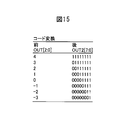
- FIG. 15 is a table showing examples of conversion codes.
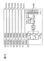
- FIG. 16 is a diagram illustrating a configuration of a parallel-serial converter in the sigma-delta modulator of the second embodiment.
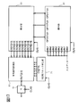
- FIG. 17 is a diagram illustrating an overall configuration of the sigma delta modulator according to the third embodiment.
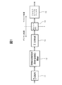
- FIG. 6 is a simplified conceptual diagram for explaining the operation of the sigma delta modulator of the first embodiment.
- the actual first embodiment is shown in FIGS.
- the sigma-delta modulator of the first embodiment is a third-order MASH type sigma-delta modulator, and is used for the sigma-delta modulator ( ⁇ Mod) 13 shown in FIG.
- the sigma-delta modulator of the first embodiment generates j-bit output data from i-bit input data.
- the sigma delta operation will be described in the case where 8 input data are processed in parallel.
- the present invention is not limited to this.
- the sigma delta modulator of the first embodiment includes a sigma delta calculation unit 31 and a parallel / serial conversion unit 61.
- the input is input to the sigma delta calculation unit 31 as 8 parallel input data.
- the sigma delta calculation unit 31 has eight sets of integration units 41A and differentiation units 51A, and executes integration calculation and differential calculation in parallel for eight pieces of input data. As will be described later, the eight sets of integration unit 41A and differentiation unit 51A are integrally formed and operated.
- the integral part and the differential part formed integrally include a plurality of operation units, and execute the operation of each stage in synchronization with the operation clock CLKi, and 8 pieces of 3-bit output data in parallel in synchronization with CLKi. Output to.
- the parallel-serial conversion unit 61 converts 8-bit 3-bit output data output in parallel in synchronization with CLKi into 3-bit output data in series and outputs the 3-bit output data in synchronization with CLK0.
- FIG. 7 is a diagram showing an overall configuration of the sigma delta modulator of the first embodiment.
- the sigma delta modulator includes an integration unit 41, a differentiation unit 51, a parallel / serial conversion unit 61, and an 8-phase clock generation unit 71.
- the 8-phase clock generator 71 supplies a clock to the parallel / serial converter 61.
- the frequency fi of the operation clock CLKi is 1/8 of the master clock frequency fs.
- the integrating unit 41 and the differentiating unit 51 operate in synchronization with the operation clock CLKi.
- the 8-phase clock generator 71 generates an 8-phase clock having a pulse width corresponding to the cycle of CLK0 from the master clock CLK0 and shifted by the cycle of CLK0 at a cycle 8 times the cycle of CLK0.
- the data is output to the conversion unit 61. Since the parallel-serial converter 61 operates based on the 8-phase clock, it operates substantially in synchronization with CLK0.
- the integration unit 41 receives eight 10-bit input data in parallel and performs an integration operation, and three sets of integration data OF0 to OF2 including 8 parallel operation results are obtained as a differentiation unit 51. Output in parallel in synchronization with CLKi.
- the differentiating unit 51 receives the integration data OF0 to OF2, performs differentiation, and outputs 7-parallel differential data SD0 to SD7 including a 3-bit operation result to the parallel-serial conversion unit 61 in parallel in synchronization with CLKi. .
- the parallel-serial converter 61 receives the differential data SD0 to SD7 in parallel, converts them into serial output data OUT, and outputs them in synchronization with CLK0.
- the integration unit 41 and the differentiation unit 51 perform the integral operation and the differentiation operation with a large amount of calculation on eight pieces of data in parallel, so that even if the operating frequency is lowered, the operation can be performed at high speed. It can be processed.
- the parallel data obtained as a result of the parallel processing is converted into serial data by the parallel-serial converter 61 capable of high-speed operation and output as high-speed data. As a result, a sigma delta modulator operating at high speed can be realized.
- FIG. 8 is a diagram illustrating a configuration example of the integration unit 41.
- the integrating unit 41 has an 8-parallel tertiary (three-stage) configuration and receives the input data IN0 to IN7 in parallel.
- Each stage of the integration unit 41 has a parallel integration unit.
- Each stage of the parallel integration unit includes an input data addition unit and a parallel integration unit.
- reference numeral 42 indicates a first-stage input data adder
- 43 indicates a first-stage parallel integrator.
- parallel integration units having an input data addition unit and a parallel integration unit are similarly provided in the second and third stages.
- the first stage input data adder 42 includes a sequence of seven input data adders SA01 to SA07.
- SA01 adds IN0 and IN1 and outputs the added value.
- SA02 adds the output of SA01 and IN2, and outputs an added value.
- the Xth SA0X adds the output of SA0 (X ⁇ 1) in the previous stage and INX to output an added value.
- the structure which performs the calculation equivalent to this may be sufficient.
- the first-stage parallel integration unit 43 includes a series of eight parallel integrators including input adders AD00 to AD07 and flip-flops SF00 to SF07. A set of one input adder and one flip-flop forms an integrator.
- AD00 adds the input data IN0 and the output of SF07.
- SF00 holds the output of AD10 and outputs it in synchronization with CLKi.
- the overflow output of AD00 is output as OF0 ⁇ 0>.
- AD01 adds the output of SA01 and the output of SF07.
- SF01 holds the output of AD01 and outputs it in synchronization with CLKi.
- the overflow output of AD01 is output as OF0 ⁇ 1>.
- the integration unit including AD00 and SF00 calculates and outputs an integration value obtained by adding the newly input input data IN0 to the integration value of the input data one clock before output by SF07.
- the integration unit including AD01 and SF01 calculates and outputs an integral value obtained by adding newly inputted input data IN0 and IN1 to the integral value of the input data one clock before output from SF07.
- the integration unit including AD07 and SF07 calculates and outputs an integral value obtained by adding newly inputted input data IN0 to IN7 to the integrated value of input data one clock before output from SF07. .
- the overflow outputs of the adders AD00 to AD07 are OF0 ⁇ 0> to OF0 ⁇ 7>.
- OF0 ⁇ 7> one clock before is OF0 ′ ⁇ 7>
- Data exceeding the number of bits of the input data (IN0) is output as OF0 ⁇ 0>.
- AD07 output IN0 + IN1 + IN2 + IN3 + IN4 + IN5 + IN6 + IN7 + OF0 ′ ⁇ 7> and OF0 ′ ⁇ 7> are output, and eight integrations (additions) are simultaneously performed in one cycle of CLKi.
- OF0 ⁇ 1> takes a cumulative overflow value when integration is performed twice for the two data IN0 and IN1, and similarly, OF0 ⁇ 7> is for the eight data IN0-7. Cumulative overflow occurs when integrating 8 times.
- the second-stage input data adder also includes a sequence of seven input data adders SA11 to SA17, and the second-stage parallel integrator also includes eight sets including input adders AD10 to AD17 and flip-flops SF10 to SF17. Contains a series of parallel integrators.
- SA11 adds the outputs of SF00 and SF01 and outputs the added value.
- SA12 adds the output of SA11 and the output of SF02 and outputs the added value.
- the Xth SA1X adds the output of SA1 (X-1) and the output of the first stage SF0X and outputs the added value.
- AD10 adds the output of SF00 and the output of SF17.
- SF10 holds the output of AD10 and outputs it in synchronization with CLKi.
- the overflow of AD10 is output as OF1 ⁇ 0>.
- AD11 adds the output of SA11 and the output of SF17.
- SF11 holds the output of AD11 and outputs it in synchronization with CLKi.
- the overflow of AD11 is output as OF1 ⁇ 1>.
- the Xth AD1X adds the output of SF00 or the corresponding SA1X and the output of SF17, and SF1X holds the output of AD1X and outputs it in synchronization with CLKi.
- the overflow output of AD1X is output as OF1 ⁇ X>.
- the integrator including AD10 and SF10 calculates and outputs an integrated value obtained by adding the output of SF00 newly input from the first stage to the integrated value of the input data one clock before output from SF17.
- the integration unit including AD17 and SF17 calculates and outputs an integration value obtained by adding the outputs of SF00 to SF07 in the first stage to the integration value of the input data one clock before output from SF17.
- the eight integration units perform integration calculations.
- the overflow outputs of the input adders AD10 to AD17 are OF1 ⁇ 0> to OF1 ⁇ 7>.
- the second stage parallel integration unit performs eight parallel integrations.
- the third-stage input data adder also includes a row of seven input data adders SA21 to SA27.
- the third-stage parallel integration unit includes eight input adders AD20 to AD27, but includes only one flip-flop SF27 corresponding to the eighth AD27, and a flip-flop corresponding to AD20 to AD26 is provided. Not. Therefore, the third-stage parallel integrator is provided with an integrator for adding the output of SA27, but no other integrator is provided. This is because the output of AD20 to AD26 does not need to be used in the next stage because the sigma delta modulator of the first embodiment is third order and there is no fourth stage.
- SA21 adds the outputs of SF10 and SF11 and outputs the added value.
- SA22 adds the output of SA21 and the output of SF12 and outputs the added value.
- the Xth SA2X adds the output of SA2 (X-1) and the output of SF1X, and outputs an added value.
- AD20 adds the output of SF10 and the output of SF27.
- the overflow of AD20 is output as OF2 ⁇ 0>.
- AD21 adds the output of SA21 and the output of SF27.
- the overflow of AD21 is output as OF2 ⁇ 1>.
- the Xth AD2X adds the output of SF10 or the corresponding SA2X and the output of SF27, and the overflow output of AD2X is output as OF2 ⁇ X>.
- AD27 adds the output of SA27 and the output of SF27, and SF27 holds the output of AD27 and outputs it in synchronization with CLKi.
- the overflow of AD27 is output as OF2 ⁇ 7>.
- the third-stage parallel integration unit also performs 8-parallel integration or addition.
- the eight parallel integrators in each stage respectively calculate data for eight master clocks in parallel with the operation clock CLKi, and three sets of eight parallel data OF0 ⁇ 0 to 7>, OF1 ⁇ 0-7>, OF2 ⁇ 0-7> are output.
- the integration calculation result (overflow) for the input data is transmitted in parallel to the differentiation unit 51 as the output of the integration unit 41.
- FIG. 9 is a diagram illustrating a configuration example of the differentiating unit 51.
- the differentiation unit 51 has three parallel differentiation units corresponding to the first to third stages of parallel integration units.
- the parallel differentiating unit corresponding to the third stage parallel integrating unit has seven input differentiators DS21 to DS27, a flip-flop DF1, and a parallel differentiator including eight subtractors DIF10 to DIF17.
- the flip-flop DF1 holds the output of DS27 and outputs it in synchronization with CLKi.
- OF2 ⁇ 1> takes a cumulative overflow value when the two data of SF10 and SF11 are integrated twice, and similarly, OF2 ⁇ x> is x + 1 data of SF10 to SF1x. Therefore, the integral overflow is calculated from the cumulative overflow by performing the difference calculation.
- OFD2 ⁇ 0> to OFD2 ⁇ 7> are eight parallel overflow values output in the period of CLKi (eight master clock periods).
- the subtractor DIF10 subtracts the output of DF1 from OF2 ⁇ 0> output from the third stage data adder AD20 of the integrating unit 41, that is, OFD2 ⁇ 0>, and outputs the result as DIF1 ⁇ 0>.
- the second subtracter DIF11 subtracts OFD2 ⁇ 0> from the output OFD2 ⁇ 1> of DS21 and outputs the result as DIF1 ⁇ 1>.
- the X-th subtracter DIFX subtracts OFD2 ⁇ X-1> from the output OFD2 ⁇ X> of DS2X and outputs DIF1 ⁇ X>.
- DIF1 ⁇ 0> OFD2 ⁇ 0> ⁇ DF1
- DIF1 ⁇ 1> OFD2 ⁇ 1> ⁇ OFD2 ⁇ 0>
- DIF1 ⁇ 7> OFD2 ⁇ 7> ⁇ OFD2 ⁇ 6>
- the difference of the overflow signal is taken and differential operation is performed.
- the second-stage parallel differentiating unit includes seven input differentiators DS11 to DS17, a delay unit, a sequence of eight adders TA10 to TA17, a flip-flop DF0, and eight subtractors DIF00 to DIF07. Have.
- OF1 ⁇ x> is a cumulative overflow when integrating x + 1 times with respect to x + 1 data of SF00 to SF0x. By performing this difference calculation, an overflow of one integral is calculated from the cumulative overflow. Is going. OFD1 ⁇ 0> to OFD1 ⁇ 7> are eight parallel overflow values output in the period of CLKi (eight master clock periods).
- the delay unit has eight flip-flops MF10 to MF17, holds OFD1 ⁇ 0 to 7>, and outputs in synchronization with CLKi. In other words, the delay unit delays OFD1 ⁇ 0 to 7> by one cycle of CLKi.
- TA10 to TA17 add the outputs of DIF10 to DIF17 and the outputs of MF10 to MF17, respectively, and output ADS1 ⁇ 0 to 7>.
- the flip-flop DF0 holds the output ADS1 ⁇ 7> of TA17 and outputs it in synchronization with CLKi.
- the subtractor DIF00 subtracts the output of DF0 from the output ADS1 ⁇ 7> of TA10 and outputs the result as DIF0 ⁇ 0>.
- the second subtracter DIF01 subtracts the output ADS1 ⁇ 0> of TA10 from the output ADS1 ⁇ 1> of TA11 and outputs the result as DIF0 ⁇ 1>.
- the Xth subtracter DIF0X subtracts the output ADS1 ⁇ X-1> of TA1X-1 from the output ADS1 ⁇ X> of TA1X and outputs the result as DIF ⁇ X>.
- the first-stage parallel differentiating unit has seven input differentiators DS01 to DS07, a delay unit, and a row of eight adders TA00 to TA07.
- OF0 ⁇ x> is a cumulative overflow when integration is performed x + 1 times on x + 1 data from IN0 to INx, and by performing this difference calculation, an overflow of one integral is calculated from the cumulative overflow. Is going. OFD0 ⁇ 0> to OFD0 ⁇ 7> are eight parallel overflow values output in the period of CLKi (eight master clock periods).
- the delay unit has a first set including eight flip-flops MF20 to MF27 and a second set including eight MF30 to MF37, and delays OFD0 ⁇ 0 to 7> by two CLKi cycles.
- TA00 to TA07 add the outputs of DIF00 to DIF07 and the outputs of MF30 to MF37, respectively, and output SD [0 to 7].
- SD [0] to SD [7] are each 3-bit data.
- the sigma delta modulator of the first embodiment having the integrating unit 41 shown in FIG. 8 and the differentiating unit 51 shown in FIG. 9 is compared with the general sigma delta modulator shown in FIG.
- the sigma delta modulator shown in FIG. 4 takes in and processes one input data in synchronization with one operation clock, and outputs a calculation result in synchronization with one operation clock after a predetermined time. Therefore, 8 operation clocks are required to process 8 input data.
- the sigma delta modulator of the first embodiment processes input data in parallel with one operation clock and outputs it as 8 parallel data of SD [0 to 7].
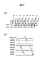
- FIG. 10 is a circuit diagram of the 8-phase clock generator 71 and a time chart showing the operation.
- the 8-phase clock generator 71 connects eight flip-flops CF0 to CF7 in series so that the output of the previous stage becomes the input of the subsequent stage, and outputs the final stage. It is a cyclic shift register that returns to the input of the first stage.
- the inverted reset signal XRST is supplied to the set terminal of the first flip-flop CF0 and to the reset terminals of the remaining flip-flops CF1 to CF7.
- the output CK [0] of CF0 becomes H and the outputs CK [1] to CK [7] of CF1 to CF7 become L by the inverted reset signal XRST.
- the inputs of CF0 and CF2 to CF7 are L and the input of CF1 is H
- CK [1] becomes H and CK [0] and CK [2] ⁇ CK [7] becomes L.
- an 8-phase shift clock having a width of the cycle of CLK0 as shown in FIG. 10B is obtained.
- the 8-phase shift clock is supplied to the parallel-serial converter 61.
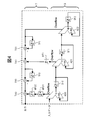
- FIG. 11 is a diagram illustrating a configuration of the parallel-serial conversion unit 61.
- FIG. 12 is a time chart showing the operation of the parallel-serial converter 61.
- the differentiation unit 51 of the sigma delta calculation unit 31 outputs SD [0] to SD [7], which are 3-bit data, in parallel.
- the parallel-serial conversion unit 61 includes three conversion processing units 620 to 622.
- the conversion processing unit 620 converts the first bit signal SD [7: 0] [0] of SD [0] to SD [7] into a serial 8-bit signal and outputs the converted output OUT [0].
- the conversion processing unit 621 converts the second bit signal SD [7: 0] [1] of SD [0] to SD [7] into a serial 8-bit signal and outputs the converted output OUT [1]. To do.
- the conversion processing unit 622 converts the third bit signal SD [7: 0] [2] of SD [0] to SD [7] into a serial 8-bit signal and outputs the converted output OUT [2]. To do. OUT [0] to OUT [2] are 3-bit conversion outputs, and the parallel-serial conversion unit 61 outputs OUT [0] to OUT [2] in synchronization with the master clock CLK0.
- the conversion processing unit 620 includes three sets of latch groups SDF0 to SDF2, a digital filter 64, a latch group SDF3, and a selector 65.
- Each of the latch groups SDF0 to SDF2 has eight latches.
- the latch group SDF0 is SD [7: 0] [0] according to CK [4]
- the latch group SDF1 is SD according to CK [5]. [7: 0] [0]
- the latch group SDF0 latches SD [7: 0] [0] according to CK [6].
- the latch group SDF3 latches SD [7: 4] [0] for 4 bits among SD [7: 0] [0] that have passed through the digital filter in accordance with CK [1].
- the digital filter 64 performs filter processing to be described later, and outputs an output SO [7: 0] [0].
- the selector 65 sequentially selects and outputs SO [3: 0] [0] and SO [7: 4] [0] output from the latch group SDF3 in accordance with the 8-phase clock of CK [7: 0]. To do.
- the conversion processing units 621 and 622 have the same configuration as the conversion processing unit 620.
- the timings of the integration unit 41 and differentiation unit 51 clocks operating at a low speed based on the operation clock CLKi and the clock timings of the parallel-serial conversion unit 61 operating at a high speed based on the master clock CLK0. For this reason, the parallel-serial conversion unit 61 to which data from the differentiating unit 51 is input receives data that is close to asynchronous data that is not guaranteed to match timing.
- the conversion processing unit 620 first performs clock transfer using a clock transfer mechanism.
- the clock transfer mechanism is formed by three sets of latch groups SDF0 to SDF2 and a digital filter.
- the 8-phase clocks CK [0] to CK [7] generated by the 8-phase clock generator 71 are shifted as indicated by P in FIG.
- the latch groups SDF0 to SDF2 receive the data SD [7: 0] from the differentiation unit 51 by the fourth to sixth sixth clocks CK [4] to CK [6].
- processing is performed by the digital filter 64 after the latch.
- a majority processing that takes a majority of three latch outputs can be used, and a majority circuit may be used as the digital filter 64.
- the data of SO [7: 4] [0] is further latched by CK [1] in the latch group SDF3.
- processing is performed so that the transition timing of the select control signal CK [7: 0] and the input signal of the selector 65 does not coincide.
- FIG. 13 is a diagram showing an output spectrum of the sigma delta modulator of the first embodiment. As shown in FIG. 13, in the first embodiment, it is understood that an operation equivalent to the general sigma delta modulator shown in FIG. 4 is performed.
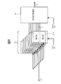
- FIG. 14 is a diagram showing an overall configuration of the sigma delta modulator according to the second embodiment.
- a code converter 81 is arranged after the differentiating unit 51, and after converting the output SD [7: 0] [2: 0] of the differentiating unit 51 into an arbitrary code,
- the difference from the first embodiment is that the input to the parallel-serial converter 61 is the same.
- FIG. 15 is a table showing examples of conversion codes.
- conversion for changing the number to be set to “1” is performed on 3-bit 8-values from ⁇ 3 to 4.
- “0” at the upper position and “1” at the lower position are consecutive, and the position where the value becomes “1” is sequentially shifted.
- FIG. 16 is a diagram illustrating a configuration of the parallel-serial conversion unit 61 in the sigma-delta modulator of the second embodiment. Since the data SD [0] to SD [7] input to the parallel / serial converter 61 are each 8-bit data, eight conversion processors are provided. Each conversion processing unit has the same configuration as the conversion processing unit 620 of FIG.
- FIG. 17 is a diagram illustrating an overall configuration of the sigma delta modulator according to the third embodiment.
- the sigma delta modulator of the third embodiment is the same as the first embodiment except that a flip-flop 91 is arranged after the parallel-serial converter 61 and the timing is adjusted again with the master clock CLK0. .
- the first and second embodiments when the phases of the eight-phase clocks of the eight-phase clock generator 71 are shifted, the shift appears in the timing of the output data.
- this deviation can be eliminated, and the timing of output data can be set with higher accuracy.
Landscapes
- Engineering & Computer Science (AREA)
- Theoretical Computer Science (AREA)
- Compression, Expansion, Code Conversion, And Decoders (AREA)
- Analogue/Digital Conversion (AREA)
Abstract
前段からのN個のデータを入力し、並列に積分演算して後段に出力するM段の並列積分ユニットを有する積分部と、積分部の対応する並列積分ユニットの隣接するオーバーフローの差分を演算すると共に差分を入力し、並列に微分演算して後段に出力する並列微分ユニットを有する微分部と、微分部からの出力を並列直列変換する並列直列変換部と、を有し、積分部の初段の並列積分ユニットは、1つの入力データを並列に受け、積分部の各段の並列積分ユニットおよび微分部の各段の並列微分ユニットは、各段の積分演算および微分演算を、マスタクロックの周波数の1/N倍の周波数の1動作クロックで実行し、並列直列変換部は、並列直列変換の結果を、マスタクロックに同期して出力するMASH方式シグマデルタ・モジュレータが提供される。
Description
本発明は、シグマデルタ・モジュレータおよびDA変換回路に関し、特にMASH方式シグマデルタ・モジュレータおよびそれを含むDAC(デジタル・アナログ変換器:Digital-to-Analog Converter)に関する。
高分解能および高速のADC(アナログ・デジタル変換器:Analog-to-Digital Converter)およびDACとして、シグマデルタ(ΣΔ)・モジュレータを用いたものが広く使用されるようになってきた。ADCにおけるシグマデルタ変換と、DACにおけるシグマデルタ変換は、逆の関係にあり、これは後述するMASH(Multistage Noise Shaping)方式についても同様である。以下のDACを例として説明する。
図1は、シグマデルタ変換を使用するシグマデルタDACの概略構成を示す図である。
図1に示すように、補間フィルタ(Interpolation filter)12は、OSR(oversampling ratio)11に基づいて、高ビット数の入力データを補間してクロック周波数を上げる。その後、シグマデルタ・モジュレータ(ΣΔMod)13は、高ビットのデータを、低ビットのデータに変換する。その後、低ビットのDAC14は、低ビットのデータをアナログ信号に変換し、アナログ信号はアナログ・ローパス・フィルタ(Analog low-pass filter)15を介して出力される。
広く知られているように、シグマデルタ・モジュレータ13は、振幅方向のみでなく、時間軸方向にも情報を持たせることで、高ビットの低速データを、低ビットの高速データ列に変換する変換器である。出力は低ビットであるが高い分解能の情報をもっている。
図2は、上記のことを、周波数領域で説明する図である。
シグマデルタDACに入力されたデータは、図2の(A)に示すように、入力データのサンプリング周期ごとに繰り返すスペクトルCを持っている。2π、4π・・・の位置にあるスペクトルCは、サンプリングによる折り返し成分であり不要成分である。シグマデルタ・モジュレータ13は、図2の(B)に示すように、サンプリング周波数を上げることで、繰り返される不要な折り返しスペクトルCを高周波側のスペクトルDにシフトする。高周波側のスペクトルDは、図2の(C)に示すように、Eで示す通過特性を有するアナログ・ローパス・フィルタ15によりカットされる。不要な折り返しスペクトルCを高周波側のスペクトルDにシフトすることにより、アナログ・ローパス・フィルタ15の通過特性への要求を低くして、アナログ・ローパス・フィルタ15への負担が低減される。これにより、チップ面積が大きくなりがちなアナログ回路への負担を低減することが可能である。
ここで、アナログ回路への負担をより一層低減するためには、シグマデルタ・モジュレータの動作周波数を、より一層上げることが望ましい。図3の(A)に示したように、シグマデルタ・モジュレータ13の動作周波数が低い場合には、サンプリングによる折り返し成分Dが直流(DC)近辺の必要なスペクトル範囲に接近しているため、急峻な通過特性Eを示す高次のローパスフィルタ15が必要である。これに対して、動作周波数が高い場合は、図3の(B)に示すように、折り返し成分D’がDCからより一層離れるため、緩い特性Eの低次のローパスフィルタを利用することが可能である。これにより、アナログ回路への負担が低減し、チップ面積の削減が実現できる。
デジタル回路で構成されたΣΔモジュレータの動作速度に限界があり、十分に動作周波数を高められない。
非特許文献1は、積分部の加算器のオーバーフローを微分して出力を得るMASH方式(Multistage Noise Shaping)のシグマデルタ・モジュレータを提案している。
図4は、非特許文献1に記載されたMASH方式のシグマデルタ・モジュレータの構成を示す図である。図4に示すシグマデルタ・モジュレータは、3次のMASH型シグマデルタ・モジュレータである。
図示のように、シグマデルタ・モジュレータは、積分部Sと、微分部Tと、を有する。積分部Sは、シグマデルタ・モジュレータの次数分だけ直列に接続された積分ユニット(図4では3段)を有する。各段の積分ユニットは、加算器AD0~AD2と、フリップフロップ(Z-1)SF0~SF2と、をそれぞれ有する。各積分ユニットは、入力データと1クロック前の演算結果との和をとることで積分を行う。積分ユニット(加算器AD0~AD2)のオーバーフローは、微分部Tに入力される。
微分部Tは、2個の微分ユニットと、2個の加算器TA0およびTA1と、フリップフロップMF01、MF02およびMF1と、を有する。1個の微分ユニットは、積分部Sの3段目の加算器AD2のオーバーフローをクロックに応じて保持するフリップフロップ(Z-1)TF1と、AD2のオーバーフローからTF1の出力を減算する減算器TS1と、を有する。MF01は、積分部Sの2段目のAD1のオーバーフローを1クロック分遅延する。TA1は、TS1とMF1の出力の加算器である。もう1個の微分ユニットは、TA1の出力を保持するTF0と、TA1の出力からTF0の出力を減算するTS0と、を有する。MF01およびMF02は、積分部Sの1段目のAD0のオーバーフローを1クロック分ずつ2段で遅延する。TA0は、TS0とMF02の出力の加算器である。各段の微分ユニットは、1クロック前のデータと現データの差分をとることで微分を行う。
図5は、図4の3次MASHシグマデルタ・モジュレータにおいて、一定DCレベルのアナログ出力を生成する場合の出力波形を示す。シグマデルタ・モジュレータの動作について、図5を参照して説明する。
出力データの瞬時値は、-4~3の8段階の低ビットのデータである。その出力データは、高速に変化しており、その平均値は、小数点以下の高分解能を表現できる。つまり、瞬間的には低ビットの離散値であるが、長周期(平均)では高分解の値となっている。周波数領域でみると、信号成分ほかに、高周波側にノイズ成分が存在するスペクトルになる。このノイズ成分は量子化ノイズといわれ、先に述べた、瞬間的な高速の変化のために発生する。
MASH方式のシグマデルタ・モジュレータについては、広く知られているので、これ以上の説明は省略する。
前述のように、量子化ノイズをDC近辺の必要なスペクトル範囲から遠ざけるためには、シグマデルタ・モジュレータを高速で動作させる必要があるが、そのためには、積分部Sおよび微分部Tを高速に動作させる必要がある。しかし、積分部Sおよび微分部Tでの演算は、大きな演算量であるため、高速動作には限界がある。
Mucahit Kizak, Izzet Kale "Rigorous Analysis of Delta-Sigma Modulators for Fractional-N PLL Frequency Synthesis" IEEE TRANSACTIONS ON CIRCUITS AND SYSTEMS-I: REGULAR PAPERS, VOL. 51, NO. 6, JUNE 2004
実施形態によれば、積分部および微分部での演算を並列化して、動作クロックの速度を実質的に向上したMASH方式シグマデルタ・モジュレータが実現される。
発明の一観点によれば、前段からのN(N;2以上の整数)個の入力を積分して後段に出力するM(M;1以上の整数)段の並列積分ユニットを有する積分部と、積分部の対応する並列積分ユニットの隣接する出力(オーバーフロー)の差分を演算すると共に差分の微分をそれぞれ演算して後段に出力する並列微分ユニットを有する微分部と、微分部からの出力を並列直列変換する並列直列変換部と、を備え、積分部の初段の並列積分ユニットは、入力データを並列に受け、積分部の各段の並列積分ユニットおよび微分部の各段の並列微分ユニットは、各段の積分演算および微分演算を、マスタクロックの周波数の1/N倍の周波数の1動作クロックで実行し、並列直列変換部は、並列直列変換の結果を、前記マスタクロックに同期して出力するMASH方式シグマデルタ・モジュレータが提供される。
発明の別の観点によれば、 オーバーサンプリングデータを発生するインターポレーションフィルタと、高ビット数のオーバーサンプリングデータを、低ビット数の変換データに変換するシグマデルタ・モジュレータと、低ビット数の変換データをアナログ信号に変換する低ビット数D/A変換器と、低ビット数D/A変換器の出力を低周波数成分を通過させるアナログ・ローパス・フィルタと、を備えるD/A変換器であって、シグマデルタ・モジュレータが、上記の発明の一観点によるMASH方式シグマデルタ・モジュレータであるD/A変換器が提供される。
発明の観点によれば、MASH方式のシグマデルタ・モジュレータの積分部および微分部での演算を並列化して、実質的に動作クロックの速度を高くして、量子化ノイズをDC近辺の必要なスペクトル範囲から遠ざけることができる。これにより、アナログ回路への負担が低減し、チップ面積を削減できる。
図6は、第1実施形態のシグマデルタ・モジュレータの動作を説明するための簡略した概念図である。なお、実際の第1実施形態は図7、8、9、10、11となる。第1実施形態のシグマデルタ・モジュレータは、3次MASH方式のシグマデルタ・モジュレータであり、図1に示したシグマデルタ・モジュレータ(ΣΔMod)13などに使用される。第1実施形態のシグマデルタ・モジュレータは、iビットの入力データからjビットの出力データを生成する。以下の説明では、i=10およびj=3として、シグマデルタ演算は、8個の入力データを並列に演算処理する場合を説明するが、これに限定されるものではない。
図6に示すように、第1実施形態のシグマデルタ・モジュレータは、シグマデルタ演算部31と、並列直列変換部61と、を有する。
入力は、8並列の入力データとして、シグマデルタ演算部31に入力される。入力データは、周波数fi(=Fs/8)(マスタクロックの8倍の周期)の動作クロックCLKiに同期している。
シグマデルタ演算部31は、積分部41Aと微分部51Aの組を8組有し、8個分の入力データに対して積分演算および微分演算を並列に実行する。後述するように、8組の積分部41Aおよび微分部51Aは、それぞれ一体に形成、演算される。一体に形成された積分部及び微分部は、複数段の演算ユニットを備え、各段の演算を、動作クロックCLKiに同期して実行し、CLKiに同期して3ビットの出力データを8個並列に出力する。
並列直列変換部61は、CLKiに同期して8個並列に出力される3ビットの出力データを直列の3ビットの出力データに変換してCLK0に同期して出力する。
図7は、第1実施形態のシグマデルタ・モジュレータの全体構成を示す図である。
図7に示すように、第1実施形態のシグマデルタ・モジュレータは、積分部41と、微分部51と、並列直列変換部61と、8位相クロック発生部71と、を有する。8位相クロック発生部71は、並列直列変換部61にクロックを供給する。上記のように、動作クロックCLKiの周波数fiは、マスタクロックの周波数fsの1/8である。積分部41および微分部51は、動作クロックCLKiに同期して動作する。8位相クロック発生部71は、マスタクロックCLK0から、CLK0の周期に対応するパルス幅を有し、CLK0の周期の8倍の周期で、CLK0の周期ずつシフトした8位相クロックを生成し、並列直列変換部61に出力する。並列直列変換部61は、8位相クロックに基づいて動作するので、実質的にCLK0に同期して動作する。
図7に示すように、積分部41は、8個の10ビットの入力データを並列に受けて積分演算を行い、8並列の演算結果を含む3組の積分データOF0~OF2を、微分部51にCLKiに同期して並列に出力する。微分部51は、積分データOF0~OF2を受けて微分演算を行い、3ビットの演算結果を含む7並列の微分データSD0~SD7を、並列直列変換部61にCLKiに同期して並列に出力する。並列直列変換部61は、微分データSD0~SD7を並列に受けて、直列の出力データOUTに変換し、CLK0に同期して出力する。
第1実施形態のシグマデルタ・モジュレータでは、積分部41および微分部51が、演算量の多い積分演算および微分演算を8個のデータについて並列に処理することで、動作周波数を下げても高速に処理できる。並列処理により得られた演算結果の並列データは、高速動作が可能な並列直列変換器61で直列データに変換されて高速データで出力される。これにより、高速動作のシグマデルタ・モジュレータを実現することができる。
次に、各部の内部構成を説明する。
図8は、積分部41の構成例を示す図である。上記のように、積分部41は、8並列の3次(3段)構成を有し、入力データIN0~IN7を並列に受ける。
積分部41の各段は並列積分ユニットを有する。各段の並列積分ユニットは、入力データ加算部と、並列積分部と、を有する。図8において、参照番号42は、1段目の入力データ加算部を、43は1段目の並列積分部を、それぞれ示す。図8に示すように、2段目および3段目にも、入力データ加算部および並列積分部を有する並列積分ユニットが、同様に設けられている。
1段目の入力データ加算部42は、7個の入力データ加算器SA01~SA07の列を含む。SA01は、IN0とIN1を加算して加算値を出力する。SA02は、SA01の出力とIN2を加算して加算値を出力する。以下同様に、X番目のSA0Xは、前段のSA0(X-1)の出力とINXを加算して加算値を出力する。また、これと等価の演算を行う構成でもよい。
したがって、SA07の出力=IN0+IN1+IN2+IN3+IN4+IN5+IN6+IN7である。
1段目の並列積分部43は、入力加算器AD00~AD07とフリップフロップSF00~SF07を含む8組の並列積分器の列を含む。1個の入力加算器と1個のフリップフロップの組が、積分器を形成する。AD00は入力データIN0とSF07の出力を加算する。SF00はAD10の出力を保持し、CLKiに同期して出力する。AD00のオーバーフロー出力はOF0<0>として出力される。AD01はSA01の出力とSF07の出力を加算する。SF01はAD01の出力を保持し、CLKiに同期して出力する。AD01のオーバーフロー出力はOF0<1>として出力される。以下同様に、X番目のAD0Xは、対応するSA0Xの出力とSF07の出力を加算し、SF0XはAD0Xの出力を保持し、CLKiに同期して出力する。AD0Xのオーバーフロー出力はOF0<X>]として出力される。したがって、AD00とSF00を含む積分ユニットは、SF07の出力する1クロック前の入力データの積分値に、新たに入力された入力データIN0を加算した積分値を演算して出力する。AD01とSF01を含む積分ユニットは、SF07の出力する1クロック前の入力データの積分値に、新たに入力された入力データIN0およびIN1を加算した積分値を演算して出力する。以下同様であり、AD07とSF07を含む積分ユニットは、SF07の出力する1クロック前の入力データの積分値に、新たに入力された入力データIN0~IN7を加算した積分値を演算して出力する。加算器AD00~AD07のオーバーフロー出力が、OF0<0>~OF0<7>である。
ここで、1クロック前のOF0<7>をOF0’<7>とすると、AD00では、入力データ(IN0)のビット数以内のデータは、AD00出力=IN0+OF0’<7>としてSF00に入力され、入力データ(IN0)のビット数を超えるデータは、OF0<0>として出力される。同様に、AD01は、AD01出力=IN0+IN1+OF0’<7>とOF0<1>が出力される。以下、同様であり、AD07は、AD07出力=IN0+IN1+IN2+IN3+IN4+IN5+IN6+IN7+OF0’<7>とOF0’<7>が出力され、CLKiの1周期で、8回分の積分(加算)を同時に行うことになる。
ここで、OF0<1>はIN0とIN1の2つのデータに対して2回積分を行ったさいの累積オーバーフロー値をとり、同様に、OF0<7>はIN0~7の8つのデータに対して8回積分を行った際の累積オーバーフローになる。
ここで、1クロック前のOF0<7>をOF0’<7>とすると、AD00では、入力データ(IN0)のビット数以内のデータは、AD00出力=IN0+OF0’<7>としてSF00に入力され、入力データ(IN0)のビット数を超えるデータは、OF0<0>として出力される。同様に、AD01は、AD01出力=IN0+IN1+OF0’<7>とOF0<1>が出力される。以下、同様であり、AD07は、AD07出力=IN0+IN1+IN2+IN3+IN4+IN5+IN6+IN7+OF0’<7>とOF0’<7>が出力され、CLKiの1周期で、8回分の積分(加算)を同時に行うことになる。
ここで、OF0<1>はIN0とIN1の2つのデータに対して2回積分を行ったさいの累積オーバーフロー値をとり、同様に、OF0<7>はIN0~7の8つのデータに対して8回積分を行った際の累積オーバーフローになる。
2段目の入力データ加算部も、7個の入力データ加算器SA11~SA17の列を含み、2段目の並列積分部も、入力加算器AD10~AD17とフリップフロップSF10~SF17を含む8組の並列積分器の列を含む。
SA11は、SF00とSF01の出力を加算して加算値を出力する。SA12は、SA11の出力とSF02の出力を加算して加算値を出力する。以下同様に、X番目のSA1Xは、SA1(X-1)の出力と1段目のSF0Xの出力を加算して加算値を出力する。
AD10は、SF00の出力とSF17の出力を加算する。SF10はAD10の出力を保持し、CLKiに同期して出力する。AD10のオーバーフローはOF1<0>として出力される。AD11はSA11の出力とSF17の出力を加算する。SF11はAD11の出力を保持し、CLKiに同期して出力する。AD11のオーバーフローはOF1<1>として出力される。以下同様に、X番目のAD1Xは、SF00または対応するSA1Xの出力とSF17の出力を加算し、SF1XはAD1Xの出力を保持し、CLKiに同期して出力する。AD1Xのオーバーフロー出力はOF1<X>として出力される。したがって、AD10とSF10を含む積分器は、SF17の出力する1クロック前の入力データの積分値に、新たに1段目から入力されたSF00の出力を加算した積分値を演算して出力する。以下同様であり、AD17とSF17を含む積分ユニットは、SF17の出力する1クロック前の入力データの積分値に、1段目のSF00~SF07の出力を加算した積分値を演算して出力する。このように、8個の積分ユニットは、積分演算を行う。ここで、入力加算器AD10~AD17のオーバーフロー出力が、OF1<0>~OF1<7>である。2段目並列積分ユニットも1段目と同様に、8並列の積分を行う。
3段目の入力データ加算部も、7個の入力データ加算器SA21~SA27の列を含む。3段目の並列積分部は、8個の入力加算器AD20~AD27を含むが、8番目のAD27に対応したフリップフロップSF27を1個含むだけで、AD20~AD26に対応したフリップフロップは設けられていない。したがって、3段目の並列積分部は、SA27の出力を加算する積分器は設けられるが、それ以外の積分器は、設けられていない。これは、第1実施形態のシグマデルタ・モジュレータが3次であり、4段目が存在しないため、AD20~AD26の出力は、次段で使用する必要がないためである。
SA21は、SF10とSF11の出力を加算して加算値を出力する。SA22は、SA21の出力とSF12の出力を加算して加算値を出力する。以下同様に、X番目のSA2Xは、SA2(X-1)の出力とSF1Xの出力を加算して加算値を出力する。
AD20は、SF10の出力とSF27の出力を加算する。AD20のオーバーフローはOF2<0>として出力される。AD21はSA21の出力とSF27の出力を加算する。AD21のオーバーフローはOF2<1>として出力される。以下同様に、X番目のAD2Xは、SF10または対応するSA2Xの出力とSF27の出力を加算し、AD2Xのオーバーフロー出力はOF2<X>として出力される。AD27はSA27の出力とSF27の出力を加算し、SF27はAD27の出力を保持し、CLKiに同期して出力する。AD27のオーバーフローはOF2<7>として出力される。3段目並列積分ユニットも1、2段目と同様に、8並列の積分または加算を行う。
以上の通り、各段の8個の並列積分器は、それぞれ、動作クロックCLKiで、8マスタクロック分のデータを並列に演算し、3組の8並列のデータOF0<0~7>、OF1<0~7>、OF2<0~7>を出力する。言い換えれば、第1実施形態の積分部41では、入力データに対する積分演算結果(オーバーフロー)が、積分部41の出力として、微分部51に並列に伝えられる。
図9は、微分部51の構成例を示す図である。
微分部51は、1~3段目の並列積分ユニットに対応する3つの並列微分ユニットを有する。
3段目の並列積分ユニットに対応する並列微分ユニットは、7個の入力差分器DS21~DS27と、フリップフロップDF1と、8個の減算器DIF10~DIF17を含む並列微分器と、を有する。
7個の入力差分器DS21~DS27は、積分部41の3段目の8個のデータ加算器AD20~AD27のオーバーフローであるOF2<0~7>の隣接するデータの差分を演算し、OFD2<1~7>を出力する。したがって、OFD2<1>=OF2<1>-OF2<0>、…、OFD1<7>=OF2<7>-OF2<6>である。また、OFD2<0>=OF2<0>とする。フリップフロップDF1は、DS27の出力を保持し、CLKiに同期して出力する。ここで、前述したとおりOF2<1>はSF10とSF11の2つのデータに対して2回積分を行った際の累積オーバーフロー値をとり、同様に、OF2<x>はSF10~SF1xのx+1つのデータに対してx+1回積分を行った際の累積オーバーフローであるため、差分演算を行うことで、累積オーバーフローから1積分のオーバーフローの計算を行っている。OFD2<0>~OFD2<7>はCLKiの周期(マスタクロック8周期分)で出力される8並列のオーバーフロー値になる。
減算器DIF10は、積分部41の3段目のデータ加算器AD20の出力するOF2<0>、すなわちOFD2<0>からDF1の出力を減算して、DIF1<0>として出力する。2番目の減算器DIF11は、DS21の出力OFD2<1>からOFD2<0>を減算して、DIF1<1>として出力する。以下同様に、X番目の減算器DIFXは、DS2Xの出力OFD2<X>からOFD2<X-1>を減算して、DIF1<X>を出力する。したがって、DIF1<0>=OFD2<0>-DF1、DIF1<1>=OFD2<1>-OFD2<0>、…、DIF1<7>=OFD2<7>-OFD2<6>となり、隣どうしのオーバーフロー信号の差分をとっており、微分動作を行っている。
2段目の並列微分ユニットは、7個の入力差分器DS11~DS17と、ディレイ部と、8個の加算器TA10~TA17の列と、フリップフロップDF0と、8個の減算器DIF00-DIF07と、を有する。
7個の入力差分器DS11~DS17は、積分部41の2段目の8個のデータ加算器AD10~AD17のオーバーフローであるOF1<0~7>の隣接するデータの差分を演算し、OFD1<1~7>を出力する。したがって、OFD1<1>=OF1<1>-OF1<0>、…、OFD1<7>=OF1<7>-OF1<6>である。また、OFD1<0>=OF1<0>とする。ここで、OF1<x>はSF00~SF0xのx+1つのデータに対してx+1回積分を行った際の累積オーバーフローであるため、この差分演算を行うことで、累積オーバーフローから1積分のオーバーフローの計算を行っている。OFD1<0>~OFD1<7>はCLKiの周期(マスタクロック8周期分)で出力される8並列のオーバーフロー値になる。
ディレイ部は、8個のフリップフロップMF10~MF17を有し、OFD1<0~7>を保持し、CLKiに同期して出力する。言い換えれば、ディレイ部は、OFD1<0~7>を、CLKiの1周期分遅延する。
TA10~TA17は、DIF10~DIF17の出力とMF10~MF17の出力をそれぞれ加算して、ADS1<0~7>を出力する。
フリップフロップDF0は、TA17の出力ADS1<7>を保持し、CLKiに同期して出力する。
減算器DIF00は、TA10の出力ADS1<7>からDF0の出力を減算して、DIF0<0>として出力する。2番目の減算器DIF01は、TA11の出力ADS1<1>からTA10の出力ADS1<0>を減算して、DIF0<1>として出力する。以下同様に、X番目の減算器DIF0Xは、TA1Xの出力ADS1<X>からTA1X-1の出力ADS1<X-1>を減算して、DIF<X>として出力する。したがって、DIF00~DIF07およびDF0は、TA10~TA17の出力を微分する処理を行い、微分値DIF0<0~7>を出力する。したがって、DIF0<0>=ADS1<0>-DF0、DIF0<1>=ADS1<1>-ADS1<0>、…、DIF0<7>=ADS1<7>-ADS1<6>となり、隣どうしのオーバーフロー信号の差分をとっており、微分動作を行っている。
1段目の並列微分ユニットは、7個の入力差分器DS01~DS07と、ディレイ部と、8個の加算器TA00~TA07の列と、を有する。
7個の入力差分器DS01~DS07は、積分部41の1段目の8個のデータ加算器AD00~AD07のオーバーフローであるOF0<0~7>の隣接するデータの差分を演算し、OFD0<1~7>を出力する。したがって、OFD0<1>=OF0<1>-OF0<0>、…、OFD0<7>=OF0<7>-OF0<6>である。また、OFD0<0>=OF0<0>とする。ここで、OF0<x>はIN0~INxのx+1つのデータに対してx+1回積分を行った際の累積オーバーフローであるため、この差分演算を行うことで、累積オーバーフローから1積分のオーバーフローの計算を行っている。OFD0<0>~OFD0<7>はCLKiの周期(マスタクロック8周期分)で出力される8並列のオーバーフロー値になる。
ディレイ部は、8個のフリップフロップMF20~MF27を含む第1組および8個のMF30~MF37を含む第2組を有し、OFD0<0~7>を、CLKiの2周期分遅延する。
TA00~TA07は、DIF00~DIF07の出力とMF30~MF37の出力をそれぞれ加算して、SD[0~7]を出力する。SD[0]~SD[7]は、それぞれ3ビットのデータである。
ここで、図8に示した積分部41および図9に示した微分部51を有する第1実施形態のシグマデルタ・モジュレータを、図4に示した一般的なシグマデルタ・モジュレータと対比させる。図4に示したシグマデルタ・モジュレータは、1動作クロックに同期して、1入力データを取り込んで処理して、所定時間後から、1動作クロックに同期して演算結果を出力する。したがって、8つの入力データを処理するには8動作クロックが必要である。これに対して、第1実施形態のシグマデルタ・モジュレータは、入力データを1動作クロックで並列に処理して、SD[0~7]の8並列のデータとして出力する。
図10は、8位相クロック発生部71の回路図および動作を示すタイムチャートである。
図10の(A)に示すように、8位相クロック発生部71は、8個のフリップフロップCF0~CF7を、前段の出力が後段の入力になるように直列に接続し、最終段の出力を初段の入力に戻す循環型シフトレジスタである。反転リセット信号XRSTが、初段のフリップフロップCF0のセット端子に、残りのフリップフロップCF1~CF7のリセット端子に供給される。
図10の(B)に示すように、反転リセット信号XRSTにより、CF0の出力CK[0]がHに、CF1~CF7の出力CK[1]~CK[7]がLになる。この状態では、CF0およびCF2~CF7の入力はL、CF1の入力がHであるから、マスタクロックCLK0が入力されると、CK[1]がHになり、CK[0]およびCK[2]~CK[7]がLになる。以下、CLK0の周期ごとに、HになるCKの位置がシフトし、循環するので、図10の(B)のようなCLK0の周期の幅を有する8位相のシフトクロックが得られる。8位相のシフトクロックは、並列直列変換部61に供給される。
図11は、並列直列変換部61の構成を示す図である。図12は、並列直列変換部61の動作を示すタイムチャートである。
上記のように、シグマデルタ演算部31の微分部51は、3ビットのデータであるSD[0]~SD[7]を並列に出力する。並列直列変換部61は、3つの変換処理部620~622を有する。変換処理部620は、SD[0]~SD[7]の1ビット目の信号SD[7:0][0]を直列の8ビットの信号に変換して、変換出力OUT[0]を出力する。変換処理部621は、SD[0]~SD[7]の2ビット目の信号SD[7:0][1]を直列の8ビットの信号に変換して、変換出力OUT[1]を出力する。変換処理部622は、SD[0]~SD[7]の3ビット目の信号SD[7:0][2]を直列の8ビットの信号に変換して、変換出力OUT[2]を出力する。OUT[0]~OUT[2]が3ビットの変換出力であり、並列直列変換部61は、マスタクロックCLK0に同期してOUT[0]~OUT[2]を出力する。
変換処理部620は、3組のラッチ群SDF0~SDF2と、デジタルフィルタ64と、ラッチ群SDF3と、セレクタ65と、を有する。ラッチ群SDF0~SDF2は、それぞれ8個のラッチを有し、ラッチ群SDF0はCK[4]に応じてSD[7:0][0]を、ラッチ群SDF1はCK[5]に応じてSD[7:0][0]を、ラッチ群SDF0はCK[6]に応じてSD[7:0][0]をラッチする。ラッチ群SDF3は、CK[1]に応じてデジタルフィルタを通過したSD[7:0][0]のうちの4ビット分SD[7:4][0]をラッチする。デジタルフィルタ64は、後述するフィルタ処理を行い、出力SO[7:0][0]を出力する。セレクタ65は、CK[7:0]の8位相のクロックに応じて、SO[3:0][0]およびラッチ群SDF3の出力するSO[7:4][0]を順次選択して出力する。
変換処理部621および622は、変換処理部620と同じ構成を有する。
動作クロックCLKiに基づいて低速で動作する積分部41と微分部51クロックのタイミングと、マスタクロックCLK0に基づいて高速で動作する並列直列変換部61のクロックのタイミングは、一致することが保証されない。そのため、微分部51からのデータが入力される並列直列変換部61は、タイミングの一致が保証されない非同期に近いデータが入力されることになる。
そこで、変換処理部620は、まずクロック乗り換機構で、クロックの乗り換えを行う。クロック乗り換え機構は、3組のラッチ群SDF0~SDF2およびデジタルフィルタで形成される。8位相クロック発生部71で生成された8相のクロックCK[0]~CK[7]は、図12においてPで示すようにシフトしている。クロックCK[0]~CK[7]のうち、4~6番目の3つのクロックCK[4]~CK[6]で、ラッチ群SDF0~SDF2が微分部51からのデータSD[7:0][0]をラッチする。このとき、もし微分部51からのデータの変化エッジとラッチのクロックエッジが一致した場合、ラッチの不安定動作(メタステイブル)を起こす可能性がある。そこで、それを除去するために、ラッチの後にデジタルフィルタ64で処理を行う。ここで、デジタルフィルタ64における処理の簡単な例として、3つのラッチ出力の多数決をとる多数決処理を使用でき、デジタルフィルタ64として多数決回路を使用してもよい。そのあと、デジタルフィルタ64の出力SO[7:0][0]のうち、SO[7:4][0]のデータはさらにラッチ群SDF3でCK[1]にてラッチする。その後の選択処理で、セレクト制御信号CK[7:0]とセレクタ65の入力信号の遷移タイミングが一致しないように処理を行う。
以上の処理により、図12においてQで示すように、SD[0]~SD[7]は、CK[0]からCK[7]のパルスが立ち上がる間保持され、CK[0]からCK[7]に応じて、出力OUT「0」からOUT[7]が順次出力される。
図13は、第1実施形態のシグマデルタ・モジュレータの出力スペクトルを示す図である。図13に示すように、第1実施形態では、図4に示した一般的なシグマデルタ・モジュレータと等価な演算が行われることが分かる。
図14は、第2実施形態のシグマデルタ・モジュレータの全体構成を示す図である。
第2実施形態のシグマデルタ・モジュレータは、微分部51の後にコード変換器81を配置して、微分部51の出力SD[7:0][2:0]を任意のコードに変換した後、並列直列変換部61に入力するようにしたことが、第1実施形態と異なり、他は同じである。
図15は、変換コードの例を示す表である。この例では、3ビットの-3から4までの8値に対して、“1”にする個数を変化させる変換が行われる。変換後の8ビットのデータでは、上位に“0”が下位に“1”が連続し、“1”になる位置が順にシフトする。
図16は、第2実施形態のシグマデルタ・モジュレータにおける並列直列変換部61の構成を示す図である。並列直列変換部61に入力されるデータSD[0]~SD[7]が、それぞれ8ビットのデータになるため、8個の変換処理部が設けられる。各変換処理部は、図11の変換処理部620と同じ構成を有する。
図17は、第3実施形態のシグマデルタ・モジュレータの全体構成を示す図である。
第3実施形態のシグマデルタ・モジュレータは、並列直列変換部61の後にフリップフロップ91を配置し、マスタクロックCLK0でタイミングの再調整を行うことが、第1実施形態と異なり、他は同じである。第1および第2実施形態では、8位相クロック発生部71の8相のクロックの位相がずれてしまった場合、そのずれが出力データのタイミングに表れてしまう。これに対して、第3実施形態では、このずれをなくすことが可能であり、出力データのタイミングをより高精度に設定できる。
以上、第1から第実施形態を説明したが、各種の変形例が可能であるのはいうまでもない。例えば、上記の実施形態では、3次MASH方式のシグマデルタ・モジュレータで、8個のデータを並列に処理する例を説明したが、MASH方式の次数、並列に処理するデータ数等を他の値とすることが可能であるのは、当業者であれば容易に理解可能である。
以上、実施形態を説明したが、ここに記載したすべての例や条件は、発明および技術に適用する発明の概念の理解を助ける目的で記載されたものであり、特に記載された例や条件は発明の範囲を制限することを意図するものではなく、明細書のそのような例の構成は発明の利点および欠点を示すものではない。発明の実施形態を詳細に記載したが、各種の変更、置き換え、変形が発明の精神および範囲を逸脱することなく行えることが理解されるべきである。
12 補間フィルタ
13 シグマデルタ・モジュレータ(ΣΔMod)
14 低ビットDAC
15 アナログ・ロウパス・フィルタ
21 入力データ保持部
31 シグマデルタ演算部
41 積分部
51 微分部
61 並列直列変換部
71 8位相クロック発生部
13 シグマデルタ・モジュレータ(ΣΔMod)
14 低ビットDAC
15 アナログ・ロウパス・フィルタ
21 入力データ保持部
31 シグマデルタ演算部
41 積分部
51 微分部
61 並列直列変換部
71 8位相クロック発生部
Claims (10)
- 前段からのN(N;2以上の整数)個のデータを入力し、並列に積分演算して後段に出力するM(M;1以上の整数)段の並列積分ユニットを有する積分部と、
前記積分部の対応する前記並列積分ユニットの隣接するオーバーフローの差分を演算すると共に前記差分を入力し、並列に微分演算して後段に出力する並列微分ユニットを有する微分部と、
前記微分部からの出力を並列直列変換する並列直列変換部と、を備え、
前記積分部の初段の前記並列積分ユニットは、1つの入力データを並列に受け、
前記積分部の各段の前記並列積分ユニットおよび前記微分部の各段の前記並列微分ユニットは、各段の積分演算および微分演算を、マスタクロックの周波数の1/N倍の周波数の1動作クロックで実行し、
前記並列直列変換部は、前記並列直列変換の結果を、前記マスタクロックに同期して出力することを特徴とするMASH方式シグマデルタ・モジュレータ。 - 前記微分部の出力を別データに変換するデータ変換部を、さらに備え、
前記並列直列変換部は、前記データ変換部からの出力を並列直列変換する請求項1記載のMASH方式シグマデルタ・モジュレータ。 - 前記並列直列変換部の出力する前記並列直列変換の結果を保持するデータ保持部を、さらに備える請求項1または2記載のMASH方式シグマデルタ・モジュレータ。
- 前記並列積分ユニットは、
N-1個の入力加算器と、N個の単位積分器と、を備え、
X番目(Xは2~N)の入力加算器は、1番目の入力からX番目までの入力の総和を演算し、
各単位積分器は、データ加算器と、データ保持ユニットと、を備え、
1番目の前記単位積分器のデータ加算器は、1番目の入力とN番目の前記単位積分器に保持されたデータとを加算し、2番目以降のデータ加算器は、対応する前記入力加算器の出力とN番目の前記単位積分器に保持されたデータとを加算し、前記データ保持ユニットは、対応する前記データ加算器の出力を保持して、前記動作クロックに同期して出力し、
各段のN個の前記単位積分器のN個の前記データ加算器のオーバーフローが、対応する前記並列微分ユニットに出力される請求項1から3のいずれか1項記載のMASH方式シグマデルタ・モジュレータ。 - M段目の前記並列積分ユニットでは、N番目以外の前記単位積分器の前記データ保持ユニットが除かれている請求項4記載のMASH方式シグマデルタ・モジュレータ。
- M段目の前記並列積分ユニットに対応する前記M段目の並列微分ユニットは、M段目のN個の前記データ加算器の隣接するオーバーフローの差分を演算するN-1個の入力差分器と、N-1番目の入力差分器出力を前記動作クロックのタイミングで保持するフリップフロップ群Mと、M段目の前記並列積分ユニットの1番目の前記データ加算器のオーバーフローと前記フリップフロップ群Mに保持された値の減算を行う単位微分器と、N-1個の前記入力差分器の隣接する出力の差分をとるN-1個の単位微分器と、を備え、
1段目とM段目以外の前記並列微分ユニットは、M-1段目から2段目の対応する段のN個の前記データ加算器の隣接するオーバーフローの差分を演算するN-1個の入力差分器と、M-1段目から2段目の対応する段の1番目の前記データ加算器のオーバーフローとN-1個の前記入力差分器の出力を段に応じたクロック数分遅延するディレイ部と、前段のN個の前記単位微分器の出力と前記ディレイ部の出力をそれぞれ加算するN個の加算器と、前記N番目の加算器出力を前記動作クロックのタイミングで保持するフリップフロップ群M-1と、前記フリップフロップ群M-1のデータと前記1番目の加算器の出力の差分を演算する単位微分器と、前記N個の加算器の隣接する出力のN個の差分をとるN-1個の単位微分器と、を備え、
1段目の前記並列微分ユニットは、1段目のN個の前記データ加算器の隣接するオーバーフローの差分を演算するN-1個の入力差分器と、1段目の1番目の前記データ加算器オーバーフローとN-1個の前記入力差分器の出力をM-1クロック数分遅延するディレイ部と、前段のN個の前記単位微分器の出力と前記ディレイ部の出力をそれぞれ加算するN個の加算器と、を備える請求項4または5記載のMASH方式シグマデルタ・モジュレータ。 - 前記並列直列変換部は、N段の循環型シフトレジスタを有し、前記マスタクロックの周期のN倍の周期のN相のラッチクロック群を生成する請求項1から6のいずれか1項記載のMASH方式シグマデルタ・モジュレータ。
- 前記N段の循環型シフトレジスタは、N個の直列に接続されたフリップフロップを有し、最終段のフリップフロップ出力が初段のフリップフロップ入力に接続されることで循環され、N-1個のフリップフロップのリセット端子および残り1個のフリップフロップのセット端子に、リセット信号が入力される請求項7記載のMASH方式シグマデルタ・モジュレータ。
- 前記並列直列変換部は、前記微分部の出力するN個の並列データを並列に受け、
前記並列直列変換部は、
前記ラッチクロック群のうちの複数位相のラッチクロックで、前記N個の並列データをラッチする複数のラッチ群と、前記複数のラッチ群の出力をフィルタ処理するデジタルフィルタと、を有するクロック乗り換え器と、
前記デジタルフィルタの出力のうちL(L<Nの正の整数)個のデータを、前記ラッチクロック群のうちの1つの位相の前記ラッチクロックでラッチする第2ラッチ群と、
前記第2ラッチ群でラッチされたL個のデータと残りのN-L個のデータを入力とし、前記ラッチクロック群のラッチクロックを制御信号とするセレクタと、を備える請求項7または8記載のMASH方式シグマデルタ・モジュレータ。 - オーバーサンプリングデータを発生するインターポレーションフィルタと、
高ビット数の前記オーバーサンプリングデータを、低ビット数の変換データに変換するシグマデルタ・モジュレータと、
前記低ビット数の変換データをアナログ信号に変換する低ビット数D/A変換器と、
前記低ビット数D/A変換器の出力の低周波数成分を通過させるアナログ・ローパス・フィルタと、を備えるD/A変換器であって、
前記シグマデルタ・モジュレータは、請求項1から9のいずれか1項記載のMASH方式シグマデルタ・モジュレータであることを特徴とするD/A変換器。
Priority Applications (3)
| Application Number | Priority Date | Filing Date | Title |
|---|---|---|---|
| PCT/JP2011/056622 WO2012127579A1 (ja) | 2011-03-18 | 2011-03-18 | Mash方式シグマデルタ・モジュレータおよびda変換回路 |
| JP2013505639A JP5505557B2 (ja) | 2011-03-18 | 2011-03-18 | Mash方式シグマデルタ・モジュレータおよびda変換回路 |
| US14/028,905 US9007248B2 (en) | 2011-03-18 | 2013-09-17 | MASH sigma-delta modulator and DA converter circuit |
Applications Claiming Priority (1)
| Application Number | Priority Date | Filing Date | Title |
|---|---|---|---|
| PCT/JP2011/056622 WO2012127579A1 (ja) | 2011-03-18 | 2011-03-18 | Mash方式シグマデルタ・モジュレータおよびda変換回路 |
Related Child Applications (1)
| Application Number | Title | Priority Date | Filing Date |
|---|---|---|---|
| US14/028,905 Continuation US9007248B2 (en) | 2011-03-18 | 2013-09-17 | MASH sigma-delta modulator and DA converter circuit |
Publications (1)
| Publication Number | Publication Date |
|---|---|
| WO2012127579A1 true WO2012127579A1 (ja) | 2012-09-27 |
Family
ID=46878776
Family Applications (1)
| Application Number | Title | Priority Date | Filing Date |
|---|---|---|---|
| PCT/JP2011/056622 Ceased WO2012127579A1 (ja) | 2011-03-18 | 2011-03-18 | Mash方式シグマデルタ・モジュレータおよびda変換回路 |
Country Status (3)
| Country | Link |
|---|---|
| US (1) | US9007248B2 (ja) |
| JP (1) | JP5505557B2 (ja) |
| WO (1) | WO2012127579A1 (ja) |
Families Citing this family (7)
| Publication number | Priority date | Publication date | Assignee | Title |
|---|---|---|---|---|
| US9136865B2 (en) * | 2014-02-11 | 2015-09-15 | Taiwan Semiconductor Manufacturing Company, Ltd. | Multi-stage digital-to-analog converter |
| CZ2015645A3 (cs) * | 2015-09-21 | 2016-10-05 | Vysoké Učení Technické V Brně | Způsob zpracování signálu z bolometru z pole bolometrů a elektronický systém k jeho provádění |
| US9641192B1 (en) * | 2016-06-14 | 2017-05-02 | Semiconductor Components Industries, Llc | Methods and apparatus for a delta sigma ADC with parallel-connected integrators |
| CN106899291A (zh) * | 2017-02-23 | 2017-06-27 | 广东轻工职业技术学院 | 一种基于mash结构的超高频rfid系统的频率综合器 |
| US10291239B1 (en) * | 2018-06-05 | 2019-05-14 | Xilinx, Inc. | Delta-sigma modulator having expanded fractional input range |
| US11196534B1 (en) * | 2020-12-02 | 2021-12-07 | Ciena Corporation | Apparatus and methods for low power clock generation in multi-channel high speed devices |
| US11552648B2 (en) * | 2021-01-22 | 2023-01-10 | Texas Instruments Incorporated | Digital filter for a delta-sigma analog-to-digital converter |
Citations (1)
| Publication number | Priority date | Publication date | Assignee | Title |
|---|---|---|---|---|
| JP2004260791A (ja) * | 2003-02-25 | 2004-09-16 | Icom Inc | フラクショナルn周波数シンセサイザ及びシンセサイズ方法 |
Family Cites Families (10)
| Publication number | Priority date | Publication date | Assignee | Title |
|---|---|---|---|---|
| EP1093687B1 (de) | 1998-07-07 | 2002-03-13 | Infineon Technologies AG | Linearisierter multi-bit-digital/analog-wandler und seine verwendung in einem multi-bit-delta-sigma-analog/digital-wandler |
| US6707855B2 (en) * | 2002-06-20 | 2004-03-16 | Nokia Corporation | Digital delta sigma modulator in a fractional-N frequency synthesizer |
| DE60314020T2 (de) * | 2003-11-28 | 2007-09-13 | Fujitsu Ltd., Kawasaki | Sd-modulator einer pll-schaltung |
| DE102005029819B4 (de) * | 2005-06-27 | 2010-03-18 | Infineon Technologies Ag | Sigma-Delta-Umsetzer und Verwendung desselben |
| US7385539B2 (en) * | 2006-02-15 | 2008-06-10 | Texas Instruments Deutschland Gmbh | All-digital phase locked loop (ADPLL) system |
| DE102006038020B4 (de) * | 2006-08-14 | 2015-02-05 | Infineon Technologies Ag | Sigma-Delta Modulator |
| US7538706B2 (en) * | 2007-09-25 | 2009-05-26 | Mediatek Inc. | Mash modulator and frequency synthesizer using the same |
| US7911247B2 (en) * | 2008-02-26 | 2011-03-22 | Qualcomm Incorporated | Delta-sigma modulator clock dithering in a fractional-N phase-locked loop |
| JP5834377B2 (ja) * | 2010-01-13 | 2015-12-24 | 富士通株式会社 | フィルタ回路 |
| US8203475B2 (en) * | 2010-05-24 | 2012-06-19 | St-Ericsson Sa | Parallel mash ΔΣ modulator |
-
2011
- 2011-03-18 JP JP2013505639A patent/JP5505557B2/ja not_active Expired - Fee Related
- 2011-03-18 WO PCT/JP2011/056622 patent/WO2012127579A1/ja not_active Ceased
-
2013
- 2013-09-17 US US14/028,905 patent/US9007248B2/en active Active
Patent Citations (1)
| Publication number | Priority date | Publication date | Assignee | Title |
|---|---|---|---|---|
| JP2004260791A (ja) * | 2003-02-25 | 2004-09-16 | Icom Inc | フラクショナルn周波数シンセサイザ及びシンセサイズ方法 |
Also Published As
| Publication number | Publication date |
|---|---|
| JPWO2012127579A1 (ja) | 2014-07-24 |
| JP5505557B2 (ja) | 2014-05-28 |
| US20140015700A1 (en) | 2014-01-16 |
| US9007248B2 (en) | 2015-04-14 |
Similar Documents
| Publication | Publication Date | Title |
|---|---|---|
| JP5505557B2 (ja) | Mash方式シグマデルタ・モジュレータおよびda変換回路 | |
| US4703308A (en) | Apparatus and methods for digital-to-analogue conversion | |
| JP3420531B2 (ja) | デルタシグマ方式d/a変換器 | |
| US7561088B1 (en) | Multi-loop data weighted averaging in a delta-sigma DAC | |
| JPH06508484A (ja) | アナログ及びディジタル変換器 | |
| US10020818B1 (en) | Systems and methods for fast delta sigma modulation using parallel path feedback loops | |
| JPH06181438A (ja) | デジタル・デルタ−シグマ変調器 | |
| US7557744B2 (en) | PWM driver and class D amplifier using same | |
| JP2011234154A (ja) | アナログデジタル変換器およびその動作方法 | |
| JP2001094429A (ja) | アナログデジタル混在δς変調器 | |
| JP2015061269A (ja) | A/d変換装置 | |
| WO2006012493A1 (en) | High-order delta-sigma noise shaping in direct digital frequency synthesis | |
| Fitzgibbon et al. | Hardware reduction in digital delta-sigma modulators via bus-splitting and error masking—Part II: Non-constant input | |
| US5682160A (en) | High-order delta sigma analog-to-digital converter with unit-delay integrators | |
| CN108134608B (zh) | 三角积分调变器与信号转换方法 | |
| Kester | Oversampling interpolating dacs | |
| Patel et al. | Performance evaluation of different types of analog to digital converter architecture | |
| JP2001077692A (ja) | D/a変換回路 | |
| JP3048007B2 (ja) | A/d変換回路 | |
| JP2012129849A (ja) | デジタルアナログ変換装置およびその制御方法 | |
| JP2001156642A (ja) | マルチビット−デルタシグマad変換器 | |
| JPH09186600A (ja) | D/a変換装置 | |
| JP3949560B2 (ja) | 高速オーバーサンプリング変調回路 | |
| JP5491825B2 (ja) | 多段リセット可能シグマデルタアナログ/デジタル変換器 | |
| CN106656189B (zh) | 一种多级折叠内插型模数转换器及其译码方法 |
Legal Events
| Date | Code | Title | Description |
|---|---|---|---|
| 121 | Ep: the epo has been informed by wipo that ep was designated in this application |
Ref document number: 11861446 Country of ref document: EP Kind code of ref document: A1 |
|
| ENP | Entry into the national phase |
Ref document number: 2013505639 Country of ref document: JP Kind code of ref document: A |
|
| NENP | Non-entry into the national phase |
Ref country code: DE |
|
| 122 | Ep: pct application non-entry in european phase |
Ref document number: 11861446 Country of ref document: EP Kind code of ref document: A1 |