WO2012124584A1 - 固体電解コンデンサおよびその製造方法 - Google Patents
固体電解コンデンサおよびその製造方法 Download PDFInfo
- Publication number
- WO2012124584A1 WO2012124584A1 PCT/JP2012/055907 JP2012055907W WO2012124584A1 WO 2012124584 A1 WO2012124584 A1 WO 2012124584A1 JP 2012055907 W JP2012055907 W JP 2012055907W WO 2012124584 A1 WO2012124584 A1 WO 2012124584A1
- Authority
- WO
- WIPO (PCT)
- Prior art keywords
- metal
- dielectric film
- electrolytic capacitor
- solid electrolytic
- anode body
- Prior art date
- Legal status (The legal status is an assumption and is not a legal conclusion. Google has not performed a legal analysis and makes no representation as to the accuracy of the status listed.)
- Ceased
Links
Images


Classifications
-
- H—ELECTRICITY
- H01—ELECTRIC ELEMENTS
- H01G—CAPACITORS; CAPACITORS, RECTIFIERS, DETECTORS, SWITCHING DEVICES, LIGHT-SENSITIVE OR TEMPERATURE-SENSITIVE DEVICES OF THE ELECTROLYTIC TYPE
- H01G9/00—Electrolytic capacitors, rectifiers, detectors, switching devices, light-sensitive or temperature-sensitive devices; Processes of their manufacture
- H01G9/004—Details
- H01G9/022—Electrolytes; Absorbents
- H01G9/025—Solid electrolytes
- H01G9/028—Organic semiconducting electrolytes, e.g. TCNQ
-
- H—ELECTRICITY
- H01—ELECTRIC ELEMENTS
- H01G—CAPACITORS; CAPACITORS, RECTIFIERS, DETECTORS, SWITCHING DEVICES, LIGHT-SENSITIVE OR TEMPERATURE-SENSITIVE DEVICES OF THE ELECTROLYTIC TYPE
- H01G9/00—Electrolytic capacitors, rectifiers, detectors, switching devices, light-sensitive or temperature-sensitive devices; Processes of their manufacture
- H01G9/004—Details
-
- H—ELECTRICITY
- H01—ELECTRIC ELEMENTS
- H01G—CAPACITORS; CAPACITORS, RECTIFIERS, DETECTORS, SWITCHING DEVICES, LIGHT-SENSITIVE OR TEMPERATURE-SENSITIVE DEVICES OF THE ELECTROLYTIC TYPE
- H01G9/00—Electrolytic capacitors, rectifiers, detectors, switching devices, light-sensitive or temperature-sensitive devices; Processes of their manufacture
- H01G9/0029—Processes of manufacture
-
- H—ELECTRICITY
- H01—ELECTRIC ELEMENTS
- H01G—CAPACITORS; CAPACITORS, RECTIFIERS, DETECTORS, SWITCHING DEVICES, LIGHT-SENSITIVE OR TEMPERATURE-SENSITIVE DEVICES OF THE ELECTROLYTIC TYPE
- H01G9/00—Electrolytic capacitors, rectifiers, detectors, switching devices, light-sensitive or temperature-sensitive devices; Processes of their manufacture
- H01G9/004—Details
- H01G9/04—Electrodes or formation of dielectric layers thereon
- H01G9/048—Electrodes or formation of dielectric layers thereon characterised by their structure
- H01G9/052—Sintered electrodes
-
- H—ELECTRICITY
- H01—ELECTRIC ELEMENTS
- H01G—CAPACITORS; CAPACITORS, RECTIFIERS, DETECTORS, SWITCHING DEVICES, LIGHT-SENSITIVE OR TEMPERATURE-SENSITIVE DEVICES OF THE ELECTROLYTIC TYPE
- H01G9/00—Electrolytic capacitors, rectifiers, detectors, switching devices, light-sensitive or temperature-sensitive devices; Processes of their manufacture
- H01G9/004—Details
- H01G9/07—Dielectric layers
-
- H—ELECTRICITY
- H01—ELECTRIC ELEMENTS
- H01G—CAPACITORS; CAPACITORS, RECTIFIERS, DETECTORS, SWITCHING DEVICES, LIGHT-SENSITIVE OR TEMPERATURE-SENSITIVE DEVICES OF THE ELECTROLYTIC TYPE
- H01G9/00—Electrolytic capacitors, rectifiers, detectors, switching devices, light-sensitive or temperature-sensitive devices; Processes of their manufacture
- H01G9/15—Solid electrolytic capacitors
Definitions
- the present invention relates to a solid electrolytic capacitor and a manufacturing method thereof.
- a solid electrolytic capacitor includes an anode body, a dielectric film provided on the anode body, and a solid electrolyte layer provided on the dielectric film, and has an excellent performance of being small but having a large capacity.
- Manganese oxides and conductive polymers are widely used as the electrolyte constituting the solid electrolyte layer, and valve action metals such as tantalum, niobium, aluminum or titanium are widely used as the anode body material. Yes.
- valve action metals such as tantalum, niobium, aluminum or titanium are widely used as the anode body material.
- the above-described solid electrolytic capacitor is being further improved in performance.
- a technique for reducing the particle size of metal particles used in an anode body made of a sintered body has been developed.
- the surface area of the anode body can be further increased, so that the surface area of the dielectric coating can be further increased, and thus the capacity can be increased.
- Patent Documents 1 and 2 disclose a solid electrolysis including a anode body made of a sintered body of titanium and a dielectric film made of barium titanate (BaTiO 3 ) as a small and large-capacity solid electrolytic capacitor.
- a capacitor is disclosed.
- a composite metal oxide having a perovskite structure such as barium titanate has a dielectric constant 10 times or more that of the oxide formed by the above-described chemical conversion treatment. It is considered that the capacity of the capacitor can be further increased.
- a dielectric film made of barium titanate is formed on the surface of the sintered body made of titanium, but the formation of the sintered body using titanium is actually performed. There is a problem that is difficult. Further, the present inventors have found that the leakage current of the solid electrolytic capacitor provided with the dielectric film made of barium titanate is very large, and therefore the withstand voltage of the solid electrolytic capacitor is low. Therefore, it is difficult to actually provide a high-performance solid electrolytic capacitor by the techniques described in the cited documents 1 and 2.
- an object of the present invention is to provide a high performance solid electrolytic capacitor and a method for manufacturing the same.
- a first aspect of the present invention includes an anode body made of tantalum or niobium, a dielectric film provided on the anode body, and a solid electrolyte layer provided on the surface of the dielectric film. Includes a first dielectric film made of an oxide of tantalum or niobium formed on the surface of the anode body, and a second dielectric made of a composite metal oxide having a perovskite structure formed on the first dielectric film.
- a solid electrolytic capacitor including a coating.
- the composite metal oxide having a perovskite structure is preferably barium titanate.
- the second dielectric film is partially formed on the first dielectric film, and the solid electrolyte layer is a first dielectric film not covered with the second dielectric film, It is preferable that the first dielectric film and the second dielectric film are in contact with each other.
- the second aspect of the present invention comprises a step of forming an anode body made of a first metal, a metal film made of a second metal different from the first metal, and an oxide of the second metal on the surface of the anode body.
- a step of forming at least one of the metal oxide film and a chemical conversion treatment of the anode body change the first metal constituting the surface portion of the anode body into an oxide, thereby forming a first metal oxide oxide.
- a step of forming a dielectric film, and a second dielectric made of a complex metal oxide containing a second metal by changing the metal film or the metal oxide film into a complex metal oxide by hydrothermally treating the anode body.
- a method for producing a solid electrolytic capacitor comprising: a step of forming a body coating; and a step of forming a solid electrolyte layer on a dielectric coating composed of a first dielectric coating and a second dielectric coating.
- At least one of a metal film made of a second metal different from the first metal and a metal oxide film made of an oxide of the second metal is formed on the surface of the powder of the first metal.
- Sintering the first metal powder on which the metal film or metal oxide film is formed forming an anode body having the metal film or metal oxide film on the surface, and chemical conversion treatment of the anode body
- the first metal constituting the surface portion of the anode body into an oxide to form a first dielectric film made of the oxide of the first metal
- hydrothermally treating the anode body Changing the metal film or the metal oxide film into a composite metal oxide to form a second dielectric film made of the composite metal oxide containing the second metal, and the first dielectric film and the second dielectric
- a method of manufacturing a solid electrolytic capacitor comprising a.
- the first metal is tantalum or niobium and the second metal is titanium.
- the composite metal oxide preferably has a perovskite structure.
- the composite metal oxide is preferably barium titanate.
- the metal film and the metal oxide film are preferably formed so as to partially cover the surface of the anode body.
- the anode body it is preferable to subject the anode body to a chemical conversion treatment after hydrothermal treatment of the anode body.
- a high-performance solid electrolytic capacitor and a method for manufacturing the same can be provided.
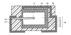
- FIG. 2 is a schematic cross-sectional view of an example of the solid electrolytic capacitor of Embodiment 1.
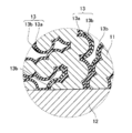
- FIG. 6 is a typical enlarged view of the area
- (A) to (E) are schematic cross-sectional views illustrating an example of a method for producing a solid electrolytic capacitor of the present invention.
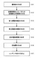
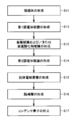
- 6 is a flowchart illustrating an example of a method for manufacturing a solid electrolytic capacitor according to Embodiment 3.
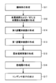
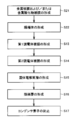
- 6 is a flowchart showing an example of a method for manufacturing the solid electrolytic capacitor of the fourth embodiment.
- 6 is a flowchart illustrating an example of a method for manufacturing a solid electrolytic capacitor according to a fifth embodiment.
- 12 is a flowchart illustrating an example of a method for manufacturing the solid electrolytic capacitor according to the sixth embodiment.
- FIG. 1 is a schematic cross-sectional view of an example of the solid electrolytic capacitor of Embodiment 1
- FIG. 2 is a schematic enlarged view of a region A shown in FIG.
- the solid electrolytic capacitor includes an anode body 11 in which an anode lead 12 is erected, a dielectric film 13 provided on the surface of the anode body 11, and a solid electrolyte layer provided on the dielectric film 13. 14. Further, on the solid electrolyte layer 14, a cathode layer in which a carbon layer 15 and a silver paint layer 16 are laminated in this order is provided, and an anode body 11, an anode lead 12, a dielectric coating 13, a solid electrolyte layer 14, The capacitor layer 10 is constituted by the carbon layer 15 and the silver paint layer 16.
- an anode terminal 17 is connected to the anode lead 12, and a cathode terminal 19 is connected to the silver paint layer 16 through an adhesive layer 18 made of a conductive adhesive. Furthermore, the capacitor element 10 is sealed with the exterior resin 20 so that a part of the anode terminal 17 and a part of the cathode terminal 19 are exposed. In FIG. 1, the exposed anode terminal 17 and cathode terminal 19 are bent along the surface of the exterior resin 20.
- the anode body 11 is a sintered body made of tantalum or niobium, and is more preferably a sintered body made of tantalum in terms of low leakage current.
- the anode body 11 on the block is shown for convenience, but more specifically, as shown in FIG. 2, a porous structure in which metal particles constituting the anode body 11 are irregularly bonded. have.
- the material of the anode lead 12 whose one end is embedded in the anode body 11 is not particularly limited as long as it is a metal, but it is preferable to use the same metal as the metal of the anode body 11.
- the dielectric coating 13 includes a first dielectric coating 13a formed on the surface of the anode body 11 and a second dielectric coating 13b formed on the first dielectric coating 13a. In addition, metal particles constituting the anode body 11 are covered.
- the first dielectric film 13a is an oxide film made of a metal oxide constituting the anode body 11, and the composition of the oxide film is expressed by a chemical formula of Ta 2 O 5 when the metal is tantalum. When the metal is niobium, it is represented by the chemical formula Nb 2 O 5 .
- the first dielectric film 13a is an oxide film generated by oxidation of the metal that constitutes the surface of the anode body 11 by chemical conversion treatment.
- the dielectric coating is formed on the surface of the anode lead 12 by the chemical conversion treatment and the anode lead 12 is made of the same metal as the anode body 11, as shown in FIG.
- the first dielectric film 13a is present.
- the second dielectric coating 13b is a composite metal oxide film made of a composite metal oxide having a perovskite structure.
- the composite metal oxide having a perovskite structure include barium titanate (BaTiO 3 ), calcium titanate (CaTiO 3 ), and strontium titanate (BaTiO 3 ).
- barium titanate is easily used as the second dielectric film 13b because it can be easily generated from titanium and has a higher dielectric constant than other metal oxides having a perovskite structure. be able to.
- the second dielectric film 13b made of a composite metal oxide having a perovskite structure has a dielectric constant 10 times higher than that of the first dielectric film 13a, which is an oxide film of tantalum and niobium. Therefore, in the present embodiment, dielectric film 13 can have a higher dielectric constant than a conventional dielectric film made of only an oxide film. Moreover, according to this Embodiment, the increase in the leakage current of a solid electrolytic capacitor resulting from providing the dielectric film which consists of barium titanate can be suppressed. The reason for this is not clear, but one of the reasons is as follows.
- the crystallinity of a composite metal oxide having a perovskite structure tends to be higher than that of a valve metal oxide. For this reason, a dielectric film made of a composite metal oxide having a perovskite structure is prone to cracks, and the leakage current increases due to the crack reaching the interface between the anode body and the dielectric film. Can be considered. In addition, a leakage current may be generated from the crystal grain boundary.
- the second dielectric film 13b and the anode body 11 are amorphous and may have a denser structure than the second dielectric film 13b.
- One dielectric coating 13a is present.
- the second dielectric film 13b may be partially formed on the first dielectric film 13a as shown in FIG.
- the solid electrolyte layer 14 is formed so as to be in contact with each of the first dielectric film 13a and the second dielectric film 13b that are not covered with the second dielectric film 13b. Since the second dielectric film 13b is partially formed on the first dielectric film 13a, an increase in leakage current of the solid electrolytic capacitor can be further effectively suppressed. The reason for this is not clear, but the above reason can be considered, and the characteristics of the material constituting the composite metal oxide having a perovskite structure may cause an increase in the leakage current of the solid electrolytic capacitor.
- the solid electrolyte layer 14 is provided on the dielectric film 13, and as shown in FIG. 2, the solid electrolyte layer 14 is also provided in the gap portion of the anode body 11.
- the material of the solid electrolyte layer 14 is not particularly limited, and manganese dioxide, TCNQ complex salt (7,7,8,8-tetracyanoquinodimethane), conductive polymer, or the like can be used.
- the conductive polymer examples include a polymer containing at least one of an aliphatic compound, an aromatic compound, a heterocyclic compound, and a heteroatom-containing compound, such as polythiophene and a derivative thereof, polypyrrole and a derivative thereof, Polyaniline and derivatives thereof, polyfuran and derivatives thereof, and the like can be used.
- the carbon layer 15 only needs to have conductivity, and for example, graphite can be used.
- the silver paint layer 16 can be composed of silver particles.
- the anode terminal 17 and the cathode terminal 19 are only required to have conductivity, and for example, a metal such as copper can be used.
- the adhesive layer 18 only needs to have conductivity and adhesiveness.
- a silver adhesive containing silver as a filler can be used.
- the material of the exterior resin 20 is not particularly limited, and for example, a known resin such as an epoxy resin can be used.
- the dielectric film 13 including the first dielectric film 13a and the second dielectric film 13b can have a higher dielectric constant than that of the conventional dielectric film. For this reason, the solid electrolytic capacitor of this Embodiment can have a larger electrostatic capacitance than before. Further, as described above, according to the solid electrolytic capacitor of the present embodiment, an increase in leakage current is also suppressed as compared with the case where the dielectric film is made of only a composite metal oxide having a perovskite structure. Therefore, according to the present embodiment, a high performance solid electrolytic capacitor can be provided.
- the homogeneity of the sintered body of titanium is low, the homogeneity of the anode body can be improved by using tantalum or niobium as the anode body 11 without using titanium.
- the sintered body made of tantalum has resistance to the hydrothermal treatment performed to form the second dielectric film 13b.
- it is a solid electrolytic capacitor provided with the anode body which consists of tantalum, it can have the anode body by which degradation of the anode body by corrosion etc. was suppressed, for example, can improve a pressure
- the leakage current of a solid electrolytic capacitor can be more effectively suppressed by using tantalum.
- the dielectric coating 13 may contain titanium oxide (for example, TiO, TiO 2 ).
- titanium oxide resulting from hydrothermal treatment or chemical conversion treatment may remain in the second dielectric coating 13b in the manufacturing process of the dielectric coating 13, but in this case,
- the solid electrolytic capacitor can exhibit the above-described effects.
- the solid electrolytic capacitor according to the present invention is not limited to a solid electrolytic capacitor having an anode body made of a sintered body as described above.
- it may be a winding type solid electrolytic capacitor provided with a metal foil made of tantalum or niobium as an anode body, or a single layer provided with a strip-shaped metal foil made of tantalum or niobium or a metal plate as an anode body
- a multilayer solid electrolytic capacitor may be used.
- FIG. 3 is a flowchart showing an example of the method for manufacturing the solid electrolytic capacitor of the second embodiment.
- FIGS. 4A to 4E are schematic diagrams illustrating an example of the method for manufacturing the solid electrolytic capacitor of the present invention.
- FIG. The configuration of the solid electrolytic capacitor manufactured in the present embodiment is the same as that of the solid electrolytic capacitor of the first embodiment.
- the anode body 11 is formed as shown in FIG.
- a powder of the first metal is prepared, and a molded body is formed by molding the powder into a desired shape in a state where one end side of the rod-shaped anode lead 12 in the longitudinal direction is embedded in the powder of the first metal.
- the molded body is sintered to form the anode body 11 having a porous structure.
- the first metal is made of any one of tantalum, niobium and aluminum. Among them, it is preferable to use tantalum or niobium because it has high resistance to hydrothermal treatment, which will be described later, and can suppress corrosion, dissolution, and the like due to hydrothermal treatment compared to aluminum, and the leakage current of the manufactured solid electrolytic capacitor is further reduced. In terms of a small point, it is more preferable to use tantalum.
- the material of the anode lead 12 is not particularly limited, but the same metal as the anode body 11 is preferably used in the manufacturing process.
- step S12 of FIG. 3 at least one of a metal film made of a second metal different from the first metal and a metal oxide film made of an oxide of the second metal is formed on the surface of the anode body 11.
- the metal coating can be formed by depositing the second metal particles on the surface of the anode body 11 using a vapor phase method such as vapor deposition or sputtering.
- the metal oxide film is formed by attaching the second metal oxide particles to the surface of the anode body 11 by using the vapor phase method or by using a liquid phase method such as an electrodeposition method or a sol-gel method. Can be formed.
- the metal film and the metal oxide film are changed to the second dielectric film 13b by a hydrothermal treatment to be described later, but the second dielectric film 13b is preferably a composite metal oxide having a perovskite structure, and contains titanium. Since the dielectric constant of the composite metal oxide having a perovskite structure is higher, the second metal is preferably titanium.
- the metal film and the metal oxide film may cover all the surfaces of the first metal particles constituting the anode body 11 or may be formed so as to partially cover the surface.
- a first dielectric film 13a is formed on the surface of the anode body 11 (see FIG. 2).
- the first dielectric film 13a can be formed by subjecting the anode body 11 having a metal film or metal oxide film formed on its surface to chemical conversion treatment.
- the anode body 11 is immersed in a chemical conversion treatment solution such as an aqueous solution of ammonium adipate and an aqueous solution of phosphoric acid of 0.01 wt% to 2 wt%, and a voltage is applied to the anode body 11 under a normal pressure environment. Apply for hours.
- the 1st metal which comprises the surface part of the anode body 11 changes to an oxide
- the 1st dielectric film 13a which consists of an oxide of a 1st metal is formed.
- the metal constituting the anode body 11 is made of Ta, Nb or Al
- the first dielectric film is made of Ta 2 O 5 , Nb 2 O 5 or Al 2 O 3 .
- a second dielectric film 13b made of a composite metal oxide containing a second metal is formed on the anode body 11 (see FIG. 2).
- the second dielectric film 13b can be formed by hydrothermally treating the anode body 11 on which the metal film or metal oxide film is formed.
- the anode body 11 having a metal film or metal oxide film formed on its surface is immersed in a hydrothermal treatment liquid and heated in a high-pressure environment for a predetermined time.
- the metal film or the metal oxide film changes to a composite metal oxide, and a second dielectric film 13b made of the composite metal oxide is formed.
- a metal film and a metal oxide film can be oxidized by said chemical conversion treatment, even if it is in the oxidized state, it can be changed to a composite metal oxide by hydrothermal treatment.
- the second dielectric film 13b made of the composite metal oxide has a higher dielectric constant than the first dielectric film 13a. Accordingly, a solid electrolytic capacitor having a larger capacitance than that of the conventional solid electrolytic capacitor is manufactured by manufacturing a solid electrolytic capacitor having not only the first dielectric film 13a but also the second dielectric film 13b. Can do.
- the second dielectric coating 13b is preferably a composite metal oxide having a perovskite structure.
- a composite metal oxide having a perovskite structure including titanium has a dielectric constant 10 times or more that of an oxide formed by a normal chemical conversion treatment, and therefore a solid electrolytic capacitor having a particularly large capacitance is required. Can be manufactured.
- Examples of the composite metal oxide having a perovskite structure including titanium include barium titanate (BaTiO 3 ), calcium titanate (CaTiO 3 ), and strontium titanate (BaTiO 3 ).
- barium titanate is easily used as the second dielectric film 13b because it can be easily generated from titanium and has a higher dielectric constant than other metal oxides having a perovskite structure. be able to.
- Barium titanate contains, for example, Ba (OH) 2 , Ba (NO 3 ) 2, etc., on the anode body 11 on which a metal film made of titanium or a metal oxide film made of titanium oxide is formed.
- the anode body 11 having the surface provided with the dielectric coating 13 is produced.
- step S ⁇ b> 15 of FIG. 3, as shown in FIG. 4C the solid electrolyte layer 14 is formed on the dielectric film 13.
- the solid electrolyte layer 14 is not particularly limited, and any known solid electrolyte can be used. In particular, it is preferable to use a conductive polymer layer because of its high conductivity.
- a method for forming the solid electrolyte layer 14 made of polythiophene by chemical polymerization will be described.
- the anode body 11 on which the dielectric film 13 is formed is immersed in a polymerization solution containing 3,4-ethylenedioxythiophene, which is an oxidant, a dopant, and a precursor of polythiophene. Infiltrate.
- the anode body 11 is pulled up from the polymerization solution, and 3,4-ethylenedioxythiophene is chemically polymerized on the dielectric film 13.
- a solid electrolyte layer 14 made of polythiophene is formed on the dielectric coating 13.
- the formation method of the solid electrolyte layer 14 is not limited above, For example, you may use any well-known method.
- step S ⁇ b> 16 of FIG. 3 As shown in FIG. 4D, a cathode layer including the carbon layer 15 and the silver paint layer 16 is formed on the solid electrolyte layer 14.
- the formation method of the carbon layer 15 and the silver paint layer 16 is not particularly limited.
- the carbon layer 15 can be formed by immersing the anode body 11 on which the solid electrolyte layer 14 is formed in a solution in which carbon particles are dispersed and then performing a drying process.
- the silver paint layer 16 can be formed, for example, by immersing the anode body 11 in a solution containing silver particles and drying the carbon layer 15 after forming the carbon layer 15.
- the capacitor element 10 is manufactured through the above steps.
- step S17 in FIG. 3 as shown in FIG. 4E, the capacitor element 10 is sealed to manufacture a solid electrolytic capacitor.
- a sealing method for example, there exists the following method.
- the anode terminal 17 is connected to the exposed end of the anode lead 12, and the adhesive layer 18 is formed on the silver paint layer 16 to connect one end of the cathode terminal 19.
- the capacitor element 10 is sealed with the exterior resin 20 so that the other ends of the anode terminal 17 and the cathode terminal 19 are exposed.
- the exposed anode terminal 17 and cathode terminal 19 are bent along the exterior resin 20 and subjected to an aging process, whereby the solid electrolytic capacitor shown in FIG. 4E is manufactured.
- a solid electrolytic capacitor including the dielectric film 13 including the first dielectric film 13a and the second dielectric film 13b can be manufactured.
- the second dielectric film 13b is made of a composite metal oxide containing a second metal different from the first metal constituting the anode body 11, and has a higher dielectric constant than that of the first dielectric film 13a.
- the second dielectric coating 13b may be formed so as to partially cover the first dielectric coating 13a (see FIG. 2). Such second dielectric coating 13b is preferable because it is easy to form. Further, when the second dielectric film is partially formed on the first dielectric film 13a, the leakage current can be further effectively reduced.
- the hydrothermal treatment method in the case of forming BaTiO 3 has been shown.
- CaTiO 3 Ca (OH) 2 , Ca (NO 3 ) 2 and the like are contained.
- SrTiO 3 is formed as the aqueous solution to be used, an aqueous solution containing Sr (OH) 2 , Sr (NO 3 ) 2 or the like can be used.
- FIG. 5 is a flowchart showing an example of a method for manufacturing the solid electrolytic capacitor of the third embodiment.
- the manufacturing method of the solid electrolytic capacitor of this embodiment is different from that of Embodiment 2 in that it includes a step of forming the first dielectric film 13a after the step of forming the second dielectric film 13b. These steps are the same as those in the second embodiment. Further, the details of each step are the same as those in the second embodiment, and the description thereof will not be repeated.
- a solid electrolytic capacitor including the dielectric film 13 including the first dielectric film 13a and the second dielectric film 13b can be manufactured.
- the solid electrolytic capacitor which has a larger electrostatic capacitance than the conventional solid electrolytic capacitor can be manufactured.
- the metal film or metal oxide film containing the second metal formed on the surface of the anode body 11 is changed to the composite metal oxide containing the second metal by hydrothermal treatment.
- the first metal constituting the surface portion of the anode body 11 is changed to an oxide of the first metal by chemical conversion treatment, and the first dielectric film 13a is formed. Is formed (step S13).
- the first dielectric film is formed by oxidizing the first metal constituting the surface portion of the anode body 11, as in the second embodiment.
- the first metal located in the portion where the leakage current is likely to be generated can be oxidized more selectively. For this reason, according to this Embodiment, a leakage current can be suppressed more effectively.
- the metal film that has not changed to the composite metal oxide can be oxidized by chemical conversion treatment. For this reason, the dielectric constant of the dielectric coating 13 can be further increased, so that a solid electrolytic capacitor having a higher capacitance can be manufactured.
- FIG. 6 is a flowchart showing an example of a method for manufacturing the solid electrolytic capacitor of the fourth embodiment.
- the manufacturing method of the solid electrolytic capacitor of this embodiment differs from Embodiment 2 in that it includes a step of forming a metal film and / or a metal oxide film after the step of forming the first dielectric film 13a.
- the other steps are the same as in the second embodiment. Further, the details of each step are the same as those in the second embodiment, and the description thereof will not be repeated.
- a solid electrolytic capacitor including the dielectric film 13 including the first dielectric film 13a and the second dielectric film 13b can be manufactured. For this reason, according to the manufacturing method of the solid electrolytic capacitor of this Embodiment, the solid electrolytic capacitor which has a larger electrostatic capacitance than the conventional solid electrolytic capacitor can be manufactured.
- the first metal constituting the surface portion of anode body 11 that is a sintered body is changed to an oxide, and the oxide of the first metal is changed.
- a metal film and / or a metal oxide film is formed on the surface of the first dielectric film 13a (step S12). That is, when the first dielectric film 13a is formed, the surface of the particles constituting the anode body 11 is exposed without being covered with the film, so that the first dielectric film 13a can be formed more uniformly.
- FIG. 7 is a flowchart showing an example of a method for manufacturing the solid electrolytic capacitor of the fifth embodiment.
- the method for manufacturing a solid electrolytic capacitor of the present embodiment is implemented in that it includes a step of forming an anode body (step S22) after a step of forming a metal film and / or a metal oxide film (step S21).
- step S22 a step of forming an anode body
- step S21 a metal film and / or a metal oxide film
- step S21 of FIG. 7 at least one of a metal film made of a second metal different from the first metal and a metal oxide film made of an oxide of the second metal is formed on the surface of the first metal particles.
- the metal coating can be formed, for example, by attaching the second metal particles to the surface of the first metal particles.
- the metal oxide film can be formed, for example, by adhering the second metal oxide particles to the surface of the first metal particles. Since the specific method is the same as the above-mentioned gas phase method and liquid phase method, the description thereof will not be repeated.
- step S22 of FIG. 7 the particles made of the first metal on which the metal film and / or the metal oxide film made of the second metal are sintered to form the anode body 11.
- the powder of the first metal prepared in step S21 was formed into a desired shape in a state where one end side in the longitudinal direction of the anode lead 12 of the rod-like body was embedded in the powder of the first metal.
- a molded body is formed.
- the molded body is sintered to form the anode body 11 having a porous structure.
- a solid electrolytic capacitor including the dielectric film 13 including the first dielectric film 13a and the second dielectric film 13b can be manufactured. For this reason, according to the manufacturing method of the solid electrolytic capacitor of this Embodiment, the solid electrolytic capacitor which has a larger electrostatic capacitance than the conventional solid electrolytic capacitor can be manufactured.
- the sintered anode body 11 has a porous structure, in the manufacturing methods of Embodiments 2 to 4, the outer surface of the anode body 11 (particles constituting the part exposed to the outside) However, it may be difficult to form a uniform coating on the inner surface of the anode body 11 (the surface portion of particles located inside the anode body). .
- the anode body 11 is formed by sintering after forming the metal film and / or the metal oxide film on the surface of the first metal particles in step S21, the inner surface is also formed. The anode body 11 having a film can be easily formed.
- the particles are sintered to form anode body 11. Therefore, a metal film or a metal oxide film can be more uniformly formed even inside the porous structure.
- the second dielectric film 13b can be formed more uniformly and with a larger surface area on the first dielectric film 13a, so that a solid electrolytic capacitor with higher capacitance can be manufactured.
- FIG. 8 is a flowchart showing an example of the method for manufacturing the solid electrolytic capacitor of the sixth embodiment.
- the manufacturing method of the solid electrolytic capacitor of this embodiment is different from that of Embodiment 5 in that it includes a step of forming the first dielectric film 13a after the step of forming the second dielectric film 13b. This step is the same as in the fifth embodiment. The details of each step are the same as those in the second embodiment and the fifth embodiment, and the description thereof will not be repeated.
- a solid electrolytic capacitor including the dielectric film 13 including the first dielectric film 13a and the second dielectric film 13b can be manufactured. For this reason, according to the manufacturing method of the solid electrolytic capacitor of this Embodiment, the solid electrolytic capacitor which has a larger electrostatic capacitance than the conventional solid electrolytic capacitor can be manufactured.
- the first metal constituting the surface portion of the anode body 11 is formed by subjecting the anode body 11 on which the second dielectric coating 13b is formed to a chemical conversion treatment.
- the first dielectric film 13a can be formed, and further, the first metal located in the portion where the leakage current is likely to be generated can be more selectively oxidized. For this reason, according to this Embodiment, a leakage current can be suppressed more effectively.
- the metal film that has not changed to the composite metal oxide can be oxidized by chemical conversion treatment. For this reason, the dielectric constant of the dielectric coating 13 can be further increased.
- the particles are sintered to form anode body 11.
- a metal film or a metal oxide film can be more uniformly formed even inside the porous structure.
- the second dielectric film 13b can be formed more uniformly and with a larger surface area on the first dielectric film 13a, so that a solid electrolytic capacitor with higher capacitance can be manufactured.
- the method for manufacturing a solid electrolytic capacitor according to the present invention is a solid having an anode body made of a sintered body as described above. It is not limited to the production of electrolytic capacitors.
- a winding type solid electrolytic capacitor including a metal foil made of tantalum or niobium as an anode body may be manufactured, and a strip-shaped metal foil made of tantalum or niobium or a metal plate as an anode body.
- a layer or multilayer solid electrolytic capacitor may be manufactured.
- Example 1 is a solid electrolytic capacitor including an anode body made of a sintered body as shown in FIG. 1, and includes a first dielectric film made of Ta 2 O 5 and a second dielectric film made of BaTiO 3. A solid electrolytic capacitor having a dielectric film containing was manufactured.
- a tantalum powder having an average primary particle size of 1.5 ⁇ m and an average secondary particle size of 50 ⁇ m was prepared.
- titanium was adhered to the surface of the prepared tantalum particles by a vapor deposition method, and a metal film made of titanium was formed on the surface of the tantalum particles.
- the average film thickness of the metal coating at this time was 50 nm.
- the average particle diameter was measured using a laser diffraction particle size distribution measuring apparatus, and the average film thickness was measured using an electron microscope.
- the tantalum powder on which the metal coating made of titanium was formed was molded into a rectangular parallelepiped with one end side in the longitudinal direction of the rod-shaped anode lead made of tantalum embedded in the tantalum powder to produce a molded body.
- the produced molded object was sintered and the anode body of the porous structure in which the end of the anode lead was embed
- the dimensions of the anode body at this time were length ⁇ width ⁇ height 4.4 mm ⁇ 3.2 mm ⁇ 1.0 mm.
- the anode body which was a sintered body, was immersed in a 0.2N Ba (OH) 2 aqueous solution and heated at 200 ° C. for 30 minutes in a 15 atm environment, and the anode body was hydrothermally treated. .
- This hydrothermal treatment changed Ti to BaTiO 3 , thereby forming a BaTiO 3 film as the second dielectric film.
- the anode body after hydrothermal treatment was immersed in a 2% by mass phosphoric acid aqueous solution, and the anode body was subjected to chemical conversion treatment by applying a voltage of 64 V to the anode body for 10 hours.
- chemical conversion treatment tantalum constituting the surface portion of the tantalum powder was changed to tantalum oxide (Ta 2 O 5 ), whereby a Ta 2 O 5 film as a first dielectric film was formed.
- Ta 2 O 5 tantalum oxide
- a dielectric coating including a BaTiO 3 film and a Ta 2 O 5 film was formed on the anode body.
- a solid electrolyte layer was formed on the dielectric coating by chemical polymerization. Specifically, first, an aqueous solution of butanol containing 3 mol / L of 3,4-ethylenedioxythiophene and 30 mol / L of ferric paratoluenesulfonate was prepared. And after immersing the anode body in which the dielectric film was formed in the said butanol solution adjusted to 25 degreeC for 5 minutes, the anode body was pulled up from the butanol solution, and was dried by leaving at room temperature for 10 minutes or more. By this operation, a polythiophene layer as a solid electrolyte layer was formed on the dielectric coating.
- a graphite particle suspension was applied and dried in the air to form a carbon layer, and further a silver paste layer was formed using a solution containing silver particles.
- the capacitor element was produced by the above operation.
- an anode terminal made of copper was welded to the anode lead, a silver adhesive was applied to the silver paste layer to form an adhesive layer, and one end of the cathode terminal made of copper was bonded to the adhesive layer. Further, the capacitor element was sealed with an exterior resin so that part of the anode terminal and the cathode terminal was exposed. After the exposed anode terminal and cathode terminal were bent along the exterior resin, an aging treatment was performed.
- the rated voltage of the manufactured solid electrolytic capacitor was 16V, and the length ⁇ width ⁇ height was 7.3 mm ⁇ 4.3 mm ⁇ 2.0 mm. In this example, 30 solid electrolytic capacitors were manufactured.
- Example 2 a solid electrolytic capacitor was produced by the same method as in Example 1 except that a metal film made of titanium having an average thickness of 120 nm was formed on the surface of the tantalum particles by vapor deposition.
- the manufactured solid electrolytic capacitor had a rated voltage of 16V, and a length ⁇ width ⁇ height of 7.3 mm ⁇ 4.3 mm ⁇ 2.0 mm.
- 30 solid electrolytic capacitors were manufactured.
- Comparative Example 1 a solid electrolytic capacitor was produced by the same method as in Example 1 except that the metal film made of titanium was not formed on the surface of the tantalum particles and hydrothermal treatment was not performed.
- the manufactured solid electrolytic capacitor had a rated voltage of 16V, and a length ⁇ width ⁇ height of 7.3 mm ⁇ 4.3 mm ⁇ 2.0 mm.
- 30 solid electrolytic capacitors were manufactured.
- Comparative Example 2 a solid electrolytic process was performed in the same manner as in Example 1 except that titanium particles having an average particle size of 30 ⁇ m were used as the metal powder constituting the anode body, and no hydrothermal treatment was performed. A capacitor was manufactured. The manufactured solid electrolytic capacitor had a rated voltage of 16V, and a length ⁇ width ⁇ height of 7.3 mm ⁇ 4.3 mm ⁇ 2.0 mm. In this comparative example, 30 solid electrolytic capacitors were manufactured. The average particle size was measured using a laser diffraction particle size distribution measuring device.
- Capacitance Ten units were extracted from each of the solid electrolytic capacitors of Examples 1 and 2 and Comparative Examples 1 and 2, and the capacitance ( ⁇ F) at a frequency of 120 Hz of each solid electrolytic capacitor was measured using an LCR meter for 4-terminal measurement. The average value of each was calculated. The results are shown in “Capacitance ( ⁇ F)” in Table 1.
- Example 1 and Example 2 were compared, and the electrostatic capacity of the solid electrolytic capacitor of Example 1 was smaller than the solid electrolytic capacitor of Example 2. This is presumably because the dielectric constant of the dielectric coating was further improved due to the thick film thickness of the BaTiO 3 film of Example 2. Further, the solid electrolytic capacitor of Example 1 had a smaller amount of leakage current than the solid electrolytic capacitor of Example 2. The reason for this is not clear, but it is considered that cracks occurred due to an increase in the thickness of the BaTiO 3 film because of its high crystallinity. It is also conceivable that the material of the BaTiO 3 film is caused by an increase in leakage current.
- Examples 1 and 2 were compared with Comparative Example 2, and the solid electrolytic capacitor of Comparative Example 2 had a high capacitance, but the amount of leakage current was extremely large. As a result, it is understood that a dielectric coating having a two-layer structure is necessary for improving the performance of the solid electrolytic capacitor.
- the present invention can be widely used in solid electrolytic capacitors and methods for manufacturing the same.
Landscapes
- Engineering & Computer Science (AREA)
- Power Engineering (AREA)
- Microelectronics & Electronic Packaging (AREA)
- Chemical & Material Sciences (AREA)
- Chemical Kinetics & Catalysis (AREA)
- Electrochemistry (AREA)
- Manufacturing & Machinery (AREA)
- Ceramic Capacitors (AREA)
- Fixed Capacitors And Capacitor Manufacturing Machines (AREA)
Abstract
Description
以下、図1および図2を用いて、本発明の固体電解コンデンサの実施の形態について説明する。図1は、実施の形態1の固体電解コンデンサの一例の模式的な断面図を、図2は、図1に示す領域Aの模式的な拡大図を示している。
以下、図2~図4を用いて、本発明の固体電解コンデンサの製造方法の一例を示す実施の形態2について説明する。図3は、実施の形態2の固体電解コンデンサの製造方法の一例を示すフローチャートであり、図4(A)~(E)は、本発明の固体電解コンデンサの製造方法の一例について図解する模式的な断面図である。なお、本実施の形態において製造される固体電解コンデンサの構成は、実施の形態1の固体電解コンデンサと同様である。
まず、図3のステップS11において、図3(A)に示すように、陽極体11を形成する。たとえば、第1金属の粉末を準備し、棒状体の陽極リード12の長手方向の一端側を第1金属の粉末に埋め込んだ状態で、当該粉末を所望の形状に成形した成形体を形成する。次に、この成形体を焼結して、多孔質構造の陽極体11を形成する。
次に、図3のステップS12において、陽極体11の表面に第1金属と異なる第2金属からなる金属被膜、および第2金属の酸化物からなる金属酸化物被膜の少なくとも一方を形成する。金属被膜は、蒸着法、スパッタ法などの気相法を用いて陽極体11の表面に第2金属の粒子を付着させることによって形成することができる。また、金属酸化物被膜は、上記気相法を用いて、または電着法、ゾル-ゲル法などの液相法を用いて陽極体11の表面に第2金属の酸化物の粒子を付着させることによって形成することができる。このような方法を用いて金属被膜または金属酸化物被膜を形成することによって、該被膜を陽極体11の表面により均一に、また高い密着性で形成することができる。
次に、図3のステップS13において、陽極体11の表面に第1誘電体被膜13aを形成する(図2参照。)。第1誘電体被膜13aは、金属被膜または金属酸化物被膜がその表面に形成された陽極体11を化成処理することによって形成することができる。
次に、図3のステップS14において、陽極体11の上に、第2金属を含む複合金属酸化物からなる第2誘電体被膜13bを形成する(図2参照。)。第2誘電体被膜13bは、金属被膜または金属酸化物被膜がその表面に形成された陽極体11を水熱処理することによって形成することができる。
次に、図3のステップS15において、図4(C)に示すように、誘電体被膜13の上に固体電解質層14を形成する。固体電解質層14は、特に限定されず、公知のいずれの固体電解質を用いることができる。特に、導電性の高さから、導電性高分子層を用いることが好ましい。以下に、ポリチオフェンからなる固体電解質層14の化学重合による形成方法の一例について説明する。
次に、図3のステップS16において、図4(D)に示すように、固体電解質層14上に、カーボン層15および銀ペイント層16を含む陰極層を形成する。カーボン層15および銀ペイント層16のそれぞれの形成方法は特に限定されない。
次に、図3のステップS17において、図4(E)に示すように、コンデンサ素子10を封止して、固体電解コンデンサを製造する。封止の方法としては、特に限定されないが、たとえば、以下の方法がある。
図5は、実施の形態3の固体電解コンデンサの製造方法の一例を示すフローチャートである。本実施の形態の固体電解コンデンサの製造方法は、第2誘電体被膜13bを形成する工程の後に第1誘電体被膜13aを形成する工程を含む点で、実施の形態2と異なっており、その他の工程は実施の形態2と同様である。また、各工程の詳細についても、実施の形態2と同様であるため、その説明は繰り返さない。
図6は、実施の形態4の固体電解コンデンサの製造方法の一例を示すフローチャートである。本実施の形態の固体電解コンデンサの製造方法は、第1誘電体被膜13aを形成する工程の後に、金属被膜および/または金属酸化物被膜を形成する工程を含む点で、実施の形態2と異なっており、その他の工程は実施の形態2と同様である。また、各工程の詳細についても、実施の形態2と同様であるため、その説明は繰り返さない。
図7は、実施の形態5の固体電解コンデンサの製造方法の一例を示すフローチャートである。本実施の形態の固体電解コンデンサの製造方法は、金属皮膜および/または金属酸化物被膜を形成する工程(ステップS21)の後に、陽極体を形成する工程(ステップS22)を含む点で、実施の形態2と異なっており、その他の工程は実施の形態1と同様である。以下、実施の形態2と異なる工程について説明する。
まず、図7のステップS21において、第1金属の粒子の表面に、第1金属とは異なる第2金属からなる金属被膜および第2金属の酸化物からなる金属酸化物被膜の少なくとも一方を形成する。金属被膜は、たとえば、第1金属の粒子の表面に第2金属の粒子を付着させることによって形成することができる。また、金属酸化物被膜は、たとえば、第1金属の粒子の表面に第2金属の酸化物の粒子を付着させることによって形成することができる。その具体的な方法は、上述の気相法および液相法と同様であるため、その説明は繰り返さない。
図8は、実施の形態6の固体電解コンデンサの製造方法の一例を示すフローチャートである。本実施の形態の固体電解コンデンサの製造方法は、第2誘電体被膜13bを形成する工程の後に第1誘電体被膜13aを形成する工程を含む点で、実施の形態5と異なっており、その他の工程は、実施の形態5と同様である。また、各工程の詳細についても、実施の形態2および実施の形態5と同様であるため、その説明は繰り返さない。
実施例1では、図1に示すような焼結体からなる陽極体を備える固体電解コンデンサであって、Ta2O5からなる第1誘電体被膜と、BaTiO3からなる第2誘電体被膜とを含む誘電体被膜を備える固体電解コンデンサを製造した。
実施例2では、蒸着法によって、タンタル粒子の表面に、平均厚みが120nmのチタンからなる金属被膜を形成した以外は、実施例1と同様の方法によって固体電解コンデンサを製造した。製造された固体電解コンデンサの定格電圧は16Vであり、縦×横×高さが7.3mm×4.3mm×2.0mmであった。なお、本実施例においては、30個の固体電解コンデンサを製造した。
比較例1では、タンタル粒子の表面にチタンからなる金属被膜を形成せず、また、水熱処理を行わなかった以外は、実施例1と同様の方法により、固体電解コンデンサを製造した。製造された固体電解コンデンサの定格電圧は16Vであり、縦×横×高さが7.3mm×4.3mm×2.0mmであった。なお、本比較例においては、30個の固体電解コンデンサを製造した。
比較例2では、陽極体を構成する金属粉末として、平均粒径が30μmのチタン粒子を用いたこと、また、水熱処理を行わなかったこと以外は、実施例1と同様の方法により、固体電解コンデンサを製造した。製造された固体電解コンデンサの定格電圧は16Vであり、縦×横×高さが7.3mm×4.3mm×2.0mmであった。なお、本比較例においては、30個の固体電解コンデンサを製造した。なお、平均粒径は、レーザ回折式粒度分布測定装置を用いて測定した。
(静電容量)
実施例1、2および比較例1、2の固体電解コンデンサからそれぞれ10個ずつ抽出し、4端子測定用のLCRメータを用いて、それぞれの固体電解コンデンサの周波数120Hzにおける容量(μF)を測定し、それぞれの平均値を算出した。この結果を表1の「容量(μF)」に示した。
実施例1、2および比較例1、2の固体電解コンデンサからそれぞれ10個ずつ抽出し、定格電圧を2分間印加し、その後の各固体電解コンデンサの漏れ電流量を測定し、実施例1、2および各比較例1、2における漏れ電流の平均値を算出した。この結果を表1の「漏れ電流(μA)」に示した。

Claims (10)
- タンタルまたはニオブからなる陽極体と、
前記陽極体の表面に設けられた誘電体被膜と、
前記誘電体被膜の上に設けられた固体電解質層とを備え、
前記誘電体被膜は、前記陽極体の表面に形成された前記タンタルまたはニオブの酸化物からなる第1誘電体被膜と、該第1誘電体被膜の上に形成されたペロブスカイト構造の複合金属酸化物からなる第2誘電体被膜とを含む、固体電解コンデンサ。 - 前記ペロブスカイト構造の複合金属酸化物は、チタン酸バリウムである、請求項1に記載の固体電解コンデンサ。
- 前記第2誘電体被膜は、前記第1誘電体被膜の上に部分的に形成されており、前記固体電解質層は、前記第2誘電体被膜に覆われていない前記第1誘電体被膜、および前記第2誘電体被膜のそれぞれに接するように形成されている、請求項1または2に記載の固体電解コンデンサ。
- 第1金属からなる陽極体を形成する工程と、
前記陽極体の表面に、前記第1金属と異なる第2金属からなる金属被膜、および前記第2金属の酸化物からなる金属酸化物被膜の少なくとも一方を形成する工程と、
前記陽極体を化成処理することによって、前記陽極体の表面部分を構成する前記第1金属を酸化物に変化させて、前記第1金属の酸化物からなる第1誘電体被膜を形成する工程と、
前記陽極体を水熱処理することによって、前記金属被膜または前記金属酸化物被膜を複合金属酸化物に変化させて、前記第2金属を含む複合金属酸化物からなる第2誘電体被膜を形成する工程と、
前記第1誘電体被膜および前記第2誘電体被膜からなる誘電体被膜の上に、固体電解質層を形成する工程と、を含む固体電解コンデンサの製造方法。 - 第1金属の粉末の表面に、前記第1金属とは異なる第2金属からなる金属被膜、および前記第2金属の酸化物からなる金属酸化物被膜の少なくとも一方を形成する工程と、
前記金属被膜または前記金属酸化物被膜が形成された第1金属の粉末を焼結して、前記金属被膜または前記金属酸化物被膜を表面に有する陽極体を形成する工程と、
前記陽極体を化成処理することによって、前記陽極体の表面部分を構成する前記第1金属を酸化物に変化させて、前記第1金属の酸化物からなる第1誘電体被膜を形成する工程と、
前記陽極体を水熱処理することによって、前記金属被膜または前記金属酸化物被膜を複合金属酸化物に変化させて、前記第2金属を含む複合金属酸化物からなる第2誘電体被膜を形成する工程と、
前記第1誘電体被膜および前記第2誘電体被膜からなる誘電体被膜の上に、固体電解質層を形成する工程と、を含む固体電解コンデンサの製造方法。 - 前記第1金属はタンタルまたはニオブであり、前記第2金属はチタンである、請求項4または5に記載の固体電解コンデンサの製造方法。
- 前記複合金属酸化物は、ペロブスカイト型構造を有する、請求項4から6のいずれかに記載の固体電解コンデンサの製造方法。
- 前記複合金属酸化物は、チタン酸バリウムである、請求項4から7のいずれかに記載の固体電解コンデンサの製造方法。
- 前記金属被膜および前記金属酸化物被膜は、前記陽極体の表面を部分的に覆うように形成される、請求項4から8のいずれかに記載の固体電解コンデンサの製造方法。
- 前記陽極体を水熱処理した後に、前記陽極体を化成処理する、請求項4から9のいずれかに記載の固体電解コンデンサの製造方法。
Priority Applications (2)
| Application Number | Priority Date | Filing Date | Title |
|---|---|---|---|
| JP2013504682A JP6010772B2 (ja) | 2011-03-15 | 2012-03-08 | 固体電解コンデンサの製造方法 |
| US14/004,805 US9431178B2 (en) | 2011-03-15 | 2012-03-08 | Solid electrolytic capacitor and method of producing same |
Applications Claiming Priority (2)
| Application Number | Priority Date | Filing Date | Title |
|---|---|---|---|
| JP2011056500 | 2011-03-15 | ||
| JP2011-056500 | 2011-03-15 |
Publications (1)
| Publication Number | Publication Date |
|---|---|
| WO2012124584A1 true WO2012124584A1 (ja) | 2012-09-20 |
Family
ID=46830657
Family Applications (1)
| Application Number | Title | Priority Date | Filing Date |
|---|---|---|---|
| PCT/JP2012/055907 Ceased WO2012124584A1 (ja) | 2011-03-15 | 2012-03-08 | 固体電解コンデンサおよびその製造方法 |
Country Status (3)
| Country | Link |
|---|---|
| US (1) | US9431178B2 (ja) |
| JP (1) | JP6010772B2 (ja) |
| WO (1) | WO2012124584A1 (ja) |
Cited By (3)
| Publication number | Priority date | Publication date | Assignee | Title |
|---|---|---|---|---|
| JP2012209289A (ja) * | 2011-03-29 | 2012-10-25 | Sanyo Electric Co Ltd | 固体電解コンデンサ及びその製造方法 |
| WO2018088574A1 (ja) * | 2016-11-14 | 2018-05-17 | 株式会社村田製作所 | 固体電解コンデンサ素子、固体電解コンデンサ及び固体電解コンデンサ素子の製造方法 |
| JPWO2018180029A1 (ja) * | 2017-03-30 | 2020-02-06 | パナソニックIpマネジメント株式会社 | 電極および電解コンデンサ並びにそれらの製造方法 |
Families Citing this family (9)
| Publication number | Priority date | Publication date | Assignee | Title |
|---|---|---|---|---|
| WO2014119312A1 (ja) * | 2013-01-31 | 2014-08-07 | 三洋電機株式会社 | 固体電解コンデンサおよびその製造方法 |
| KR102172296B1 (ko) * | 2014-04-30 | 2020-10-30 | 엘지이노텍 주식회사 | 에폭시 수지 조성물 및 이를 이용한 절연층을 포함하는 인쇄회로기판 |
| JP7034645B2 (ja) * | 2017-09-22 | 2022-03-14 | 株式会社Screenホールディングス | 基板処理方法および基板処理装置 |
| CN113168966B (zh) * | 2018-11-29 | 2024-01-16 | 京瓷Avx元器件公司 | 含有顺序气相沉积的电介质膜的固体电解电容器 |
| JP7660300B2 (ja) * | 2019-09-30 | 2025-04-11 | パナソニックIpマネジメント株式会社 | 電解コンデンサ用電極箔、電解コンデンサおよび電解コンデンサの製造方法 |
| JP7863734B2 (ja) * | 2019-11-29 | 2026-05-22 | パナソニックIpマネジメント株式会社 | 電解コンデンサ用陰極箔、電解コンデンサ、および、これらの製造方法 |
| US12327696B2 (en) * | 2020-03-27 | 2025-06-10 | Panasonic Intellectual Property Management Co., Ltd. | Electrode foil for electrolytic capacitor, electrolytic capacitor, and method for manufacturing electrolytic capacitor |
| CN118891695A (zh) * | 2022-01-31 | 2024-11-01 | 松下知识产权经营株式会社 | 电解电容器用电极箔、电解电容器以及电解电容器用电极箔的制造方法 |
| CN114678222B (zh) * | 2022-03-07 | 2024-06-07 | 广西广投正润新材料科技有限公司 | 一种采用水热原位合成多金属MOFs来诱导中高压阳极箔均匀发孔的方法 |
Citations (4)
| Publication number | Priority date | Publication date | Assignee | Title |
|---|---|---|---|---|
| JPS63126211A (ja) * | 1986-11-14 | 1988-05-30 | 松下電器産業株式会社 | 固体電解コンデンサの製造方法 |
| JPH0917685A (ja) * | 1995-06-27 | 1997-01-17 | Murata Mfg Co Ltd | コンデンサおよびその製造方法 |
| JP2000068160A (ja) * | 1998-08-19 | 2000-03-03 | Nec Corp | Ta固体電解コンデンサおよびその製造方法 |
| JP2008205112A (ja) * | 2007-02-19 | 2008-09-04 | Fujitsu Ltd | 電解コンデンサおよびその製造方法 |
Family Cites Families (6)
| Publication number | Priority date | Publication date | Assignee | Title |
|---|---|---|---|---|
| JPH0614502B2 (ja) | 1990-03-05 | 1994-02-23 | 日立エーアイシー株式会社 | 焼結型チタン酸バリウムコンデンサ |
| US5790368A (en) | 1995-06-27 | 1998-08-04 | Murata Manufacturing Co., Ltd. | Capacitor and manufacturing method thereof |
| JPH0917686A (ja) | 1995-06-27 | 1997-01-17 | Murata Mfg Co Ltd | コンデンサ |
| TW479262B (en) * | 1999-06-09 | 2002-03-11 | Showa Denko Kk | Electrode material for capacitor and capacitor using the same |
| JP2002222742A (ja) * | 2001-01-25 | 2002-08-09 | Rohm Co Ltd | 電解質コンデンサの製造方法 |
| US20070020955A1 (en) * | 2005-07-22 | 2007-01-25 | Samsung Electro-Mechanics Co., Ltd. | Fabrication method of composite metal oxide dielectric film, and composite metal oxide dielectric film fabricated thereby |
-
2012
- 2012-03-08 JP JP2013504682A patent/JP6010772B2/ja active Active
- 2012-03-08 US US14/004,805 patent/US9431178B2/en active Active
- 2012-03-08 WO PCT/JP2012/055907 patent/WO2012124584A1/ja not_active Ceased
Patent Citations (4)
| Publication number | Priority date | Publication date | Assignee | Title |
|---|---|---|---|---|
| JPS63126211A (ja) * | 1986-11-14 | 1988-05-30 | 松下電器産業株式会社 | 固体電解コンデンサの製造方法 |
| JPH0917685A (ja) * | 1995-06-27 | 1997-01-17 | Murata Mfg Co Ltd | コンデンサおよびその製造方法 |
| JP2000068160A (ja) * | 1998-08-19 | 2000-03-03 | Nec Corp | Ta固体電解コンデンサおよびその製造方法 |
| JP2008205112A (ja) * | 2007-02-19 | 2008-09-04 | Fujitsu Ltd | 電解コンデンサおよびその製造方法 |
Cited By (7)
| Publication number | Priority date | Publication date | Assignee | Title |
|---|---|---|---|---|
| JP2012209289A (ja) * | 2011-03-29 | 2012-10-25 | Sanyo Electric Co Ltd | 固体電解コンデンサ及びその製造方法 |
| WO2018088574A1 (ja) * | 2016-11-14 | 2018-05-17 | 株式会社村田製作所 | 固体電解コンデンサ素子、固体電解コンデンサ及び固体電解コンデンサ素子の製造方法 |
| JPWO2018088574A1 (ja) * | 2016-11-14 | 2019-06-24 | 株式会社村田製作所 | 固体電解コンデンサ素子、固体電解コンデンサ及び固体電解コンデンサ素子の製造方法 |
| CN109952626A (zh) * | 2016-11-14 | 2019-06-28 | 株式会社村田制作所 | 固体电解电容器元件、固体电解电容器以及固体电解电容器元件的制造方法 |
| CN109952626B (zh) * | 2016-11-14 | 2021-10-26 | 株式会社村田制作所 | 固体电解电容器元件、固体电解电容器以及固体电解电容器元件的制造方法 |
| JPWO2018180029A1 (ja) * | 2017-03-30 | 2020-02-06 | パナソニックIpマネジメント株式会社 | 電極および電解コンデンサ並びにそれらの製造方法 |
| JP7209263B2 (ja) | 2017-03-30 | 2023-01-20 | パナソニックIpマネジメント株式会社 | 電極および電解コンデンサ並びにそれらの製造方法 |
Also Published As
| Publication number | Publication date |
|---|---|
| US20130342966A1 (en) | 2013-12-26 |
| US9431178B2 (en) | 2016-08-30 |
| JPWO2012124584A1 (ja) | 2014-07-24 |
| JP6010772B2 (ja) | 2016-10-19 |
Similar Documents
| Publication | Publication Date | Title |
|---|---|---|
| JP6010772B2 (ja) | 固体電解コンデンサの製造方法 | |
| JP5289033B2 (ja) | 固体電解コンデンサ | |
| KR101554049B1 (ko) | 고체 전해 콘덴서 및 그 제조방법 | |
| CN101689429A (zh) | 电极箔及其制造方法以及电解电容器 | |
| WO2014034201A1 (ja) | 固体電解コンデンサの製造方法および固体電解コンデンサ | |
| JP6142292B2 (ja) | 固体電解コンデンサ | |
| JP2009505413A (ja) | 固体コンデンサおよびその製造方法 | |
| JP5062770B2 (ja) | 固体電解コンデンサおよびその製造方法 | |
| JP5623214B2 (ja) | 固体電解コンデンサ | |
| CN102473528B (zh) | 固体电解电容器的制造方法 | |
| JP4285523B2 (ja) | 固体電解コンデンサ用電極箔とその製造方法 | |
| JP5104008B2 (ja) | 電解コンデンサ | |
| JP4942673B2 (ja) | 固体電解コンデンサ及びその製造方法 | |
| JP3486113B2 (ja) | Ta固体電解コンデンサの製造方法 | |
| JP5274344B2 (ja) | 固体電解コンデンサ | |
| JP2008028137A (ja) | 固体電解コンデンサ | |
| JP4329800B2 (ja) | 固体電解コンデンサとその製造方法 | |
| JP5419794B2 (ja) | 固体電解コンデンサおよびその製造方法 | |
| WO2025204223A1 (ja) | 電解コンデンサ | |
| WO2024203050A1 (ja) | 電解コンデンサ | |
| JP2007173454A (ja) | 固体電解コンデンサ | |
| WO2024143172A1 (ja) | 固体電解コンデンサ | |
| JP4114700B2 (ja) | 固体電解コンデンサとその製造方法 | |
| JP2013074026A (ja) | 固体電解コンデンサおよびその製造方法 | |
| JP2004319646A (ja) | 電解コンデンサ及びその製造方法 |
Legal Events
| Date | Code | Title | Description |
|---|---|---|---|
| 121 | Ep: the epo has been informed by wipo that ep was designated in this application |
Ref document number: 12757411 Country of ref document: EP Kind code of ref document: A1 |
|
| ENP | Entry into the national phase |
Ref document number: 2013504682 Country of ref document: JP Kind code of ref document: A |
|
| WWE | Wipo information: entry into national phase |
Ref document number: 14004805 Country of ref document: US |
|
| NENP | Non-entry into the national phase |
Ref country code: DE |
|
| 122 | Ep: pct application non-entry in european phase |
Ref document number: 12757411 Country of ref document: EP Kind code of ref document: A1 |