WO2012124580A1 - 無接触給電設備 - Google Patents
無接触給電設備 Download PDFInfo
- Publication number
- WO2012124580A1 WO2012124580A1 PCT/JP2012/055898 JP2012055898W WO2012124580A1 WO 2012124580 A1 WO2012124580 A1 WO 2012124580A1 JP 2012055898 W JP2012055898 W JP 2012055898W WO 2012124580 A1 WO2012124580 A1 WO 2012124580A1
- Authority
- WO
- WIPO (PCT)
- Prior art keywords
- frequency
- power supply
- power
- voltage
- induction line
- Prior art date
- Legal status (The legal status is an assumption and is not a legal conclusion. Google has not performed a legal analysis and makes no representation as to the accuracy of the status listed.)
- Ceased
Links
Images




Classifications
-
- H—ELECTRICITY
- H02—GENERATION; CONVERSION OR DISTRIBUTION OF ELECTRIC POWER
- H02J—ELECTRIC POWER NETWORKS; CIRCUIT ARRANGEMENTS OR SYSTEMS FOR SUPPLYING OR DISTRIBUTING ELECTRIC POWER; SYSTEMS FOR STORING ELECTRIC ENERGY
- H02J50/00—Circuit arrangements or systems for wireless supply or distribution of electric power
- H02J50/10—Circuit arrangements or systems for wireless supply or distribution of electric power using inductive coupling
- H02J50/12—Circuit arrangements or systems for wireless supply or distribution of electric power using inductive coupling of the resonant type
-
- B—PERFORMING OPERATIONS; TRANSPORTING
- B60—VEHICLES IN GENERAL
- B60L—PROPULSION OF ELECTRICALLY-PROPELLED VEHICLES; SUPPLYING ELECTRIC POWER FOR AUXILIARY EQUIPMENT OF ELECTRICALLY-PROPELLED VEHICLES; ELECTRODYNAMIC BRAKE SYSTEMS FOR VEHICLES IN GENERAL; MAGNETIC SUSPENSION OR LEVITATION FOR VEHICLES; MONITORING OPERATING VARIABLES OF ELECTRICALLY-PROPELLED VEHICLES; ELECTRIC SAFETY DEVICES FOR ELECTRICALLY-PROPELLED VEHICLES
- B60L3/00—Electric devices on electrically-propelled vehicles for safety purposes; Monitoring operating variables, e.g. speed, deceleration or energy consumption
- B60L3/0023—Detecting, eliminating, remedying or compensating for drive train abnormalities, e.g. failures within the drive train
- B60L3/003—Detecting, eliminating, remedying or compensating for drive train abnormalities, e.g. failures within the drive train relating to inverters
-
- B—PERFORMING OPERATIONS; TRANSPORTING
- B60—VEHICLES IN GENERAL
- B60L—PROPULSION OF ELECTRICALLY-PROPELLED VEHICLES; SUPPLYING ELECTRIC POWER FOR AUXILIARY EQUIPMENT OF ELECTRICALLY-PROPELLED VEHICLES; ELECTRODYNAMIC BRAKE SYSTEMS FOR VEHICLES IN GENERAL; MAGNETIC SUSPENSION OR LEVITATION FOR VEHICLES; MONITORING OPERATING VARIABLES OF ELECTRICALLY-PROPELLED VEHICLES; ELECTRIC SAFETY DEVICES FOR ELECTRICALLY-PROPELLED VEHICLES
- B60L3/00—Electric devices on electrically-propelled vehicles for safety purposes; Monitoring operating variables, e.g. speed, deceleration or energy consumption
- B60L3/04—Cutting off the power supply under fault conditions
-
- B—PERFORMING OPERATIONS; TRANSPORTING
- B60—VEHICLES IN GENERAL
- B60L—PROPULSION OF ELECTRICALLY-PROPELLED VEHICLES; SUPPLYING ELECTRIC POWER FOR AUXILIARY EQUIPMENT OF ELECTRICALLY-PROPELLED VEHICLES; ELECTRODYNAMIC BRAKE SYSTEMS FOR VEHICLES IN GENERAL; MAGNETIC SUSPENSION OR LEVITATION FOR VEHICLES; MONITORING OPERATING VARIABLES OF ELECTRICALLY-PROPELLED VEHICLES; ELECTRIC SAFETY DEVICES FOR ELECTRICALLY-PROPELLED VEHICLES
- B60L53/00—Methods of charging batteries, specially adapted for electric vehicles; Charging stations or on-board charging equipment therefor; Exchange of energy storage elements in electric vehicles
- B60L53/10—Methods of charging batteries, specially adapted for electric vehicles; Charging stations or on-board charging equipment therefor; Exchange of energy storage elements in electric vehicles characterised by the energy transfer between the charging station and the vehicle
- B60L53/12—Inductive energy transfer
-
- B—PERFORMING OPERATIONS; TRANSPORTING
- B60—VEHICLES IN GENERAL
- B60L—PROPULSION OF ELECTRICALLY-PROPELLED VEHICLES; SUPPLYING ELECTRIC POWER FOR AUXILIARY EQUIPMENT OF ELECTRICALLY-PROPELLED VEHICLES; ELECTRODYNAMIC BRAKE SYSTEMS FOR VEHICLES IN GENERAL; MAGNETIC SUSPENSION OR LEVITATION FOR VEHICLES; MONITORING OPERATING VARIABLES OF ELECTRICALLY-PROPELLED VEHICLES; ELECTRIC SAFETY DEVICES FOR ELECTRICALLY-PROPELLED VEHICLES
- B60L53/00—Methods of charging batteries, specially adapted for electric vehicles; Charging stations or on-board charging equipment therefor; Exchange of energy storage elements in electric vehicles
- B60L53/30—Constructional details of charging stations
- B60L53/35—Means for automatic or assisted adjustment of the relative position of charging devices and vehicles
- B60L53/36—Means for automatic or assisted adjustment of the relative position of charging devices and vehicles by positioning the vehicle
-
- H—ELECTRICITY
- H01—ELECTRIC ELEMENTS
- H01F—MAGNETS; INDUCTANCES; TRANSFORMERS; SELECTION OF MATERIALS FOR THEIR MAGNETIC PROPERTIES
- H01F38/00—Adaptations of transformers or inductances for specific applications or functions
- H01F38/14—Inductive couplings
-
- B—PERFORMING OPERATIONS; TRANSPORTING
- B60—VEHICLES IN GENERAL
- B60L—PROPULSION OF ELECTRICALLY-PROPELLED VEHICLES; SUPPLYING ELECTRIC POWER FOR AUXILIARY EQUIPMENT OF ELECTRICALLY-PROPELLED VEHICLES; ELECTRODYNAMIC BRAKE SYSTEMS FOR VEHICLES IN GENERAL; MAGNETIC SUSPENSION OR LEVITATION FOR VEHICLES; MONITORING OPERATING VARIABLES OF ELECTRICALLY-PROPELLED VEHICLES; ELECTRIC SAFETY DEVICES FOR ELECTRICALLY-PROPELLED VEHICLES
- B60L2200/00—Type of vehicles
- B60L2200/18—Buses
-
- B—PERFORMING OPERATIONS; TRANSPORTING
- B60—VEHICLES IN GENERAL
- B60L—PROPULSION OF ELECTRICALLY-PROPELLED VEHICLES; SUPPLYING ELECTRIC POWER FOR AUXILIARY EQUIPMENT OF ELECTRICALLY-PROPELLED VEHICLES; ELECTRODYNAMIC BRAKE SYSTEMS FOR VEHICLES IN GENERAL; MAGNETIC SUSPENSION OR LEVITATION FOR VEHICLES; MONITORING OPERATING VARIABLES OF ELECTRICALLY-PROPELLED VEHICLES; ELECTRIC SAFETY DEVICES FOR ELECTRICALLY-PROPELLED VEHICLES
- B60L2210/00—Converter types
- B60L2210/10—DC to DC converters
-
- B—PERFORMING OPERATIONS; TRANSPORTING
- B60—VEHICLES IN GENERAL
- B60L—PROPULSION OF ELECTRICALLY-PROPELLED VEHICLES; SUPPLYING ELECTRIC POWER FOR AUXILIARY EQUIPMENT OF ELECTRICALLY-PROPELLED VEHICLES; ELECTRODYNAMIC BRAKE SYSTEMS FOR VEHICLES IN GENERAL; MAGNETIC SUSPENSION OR LEVITATION FOR VEHICLES; MONITORING OPERATING VARIABLES OF ELECTRICALLY-PROPELLED VEHICLES; ELECTRIC SAFETY DEVICES FOR ELECTRICALLY-PROPELLED VEHICLES
- B60L2210/00—Converter types
- B60L2210/30—AC to DC converters
-
- B—PERFORMING OPERATIONS; TRANSPORTING
- B60—VEHICLES IN GENERAL
- B60L—PROPULSION OF ELECTRICALLY-PROPELLED VEHICLES; SUPPLYING ELECTRIC POWER FOR AUXILIARY EQUIPMENT OF ELECTRICALLY-PROPELLED VEHICLES; ELECTRODYNAMIC BRAKE SYSTEMS FOR VEHICLES IN GENERAL; MAGNETIC SUSPENSION OR LEVITATION FOR VEHICLES; MONITORING OPERATING VARIABLES OF ELECTRICALLY-PROPELLED VEHICLES; ELECTRIC SAFETY DEVICES FOR ELECTRICALLY-PROPELLED VEHICLES
- B60L2210/00—Converter types
- B60L2210/40—DC to AC converters
-
- B—PERFORMING OPERATIONS; TRANSPORTING
- B60—VEHICLES IN GENERAL
- B60L—PROPULSION OF ELECTRICALLY-PROPELLED VEHICLES; SUPPLYING ELECTRIC POWER FOR AUXILIARY EQUIPMENT OF ELECTRICALLY-PROPELLED VEHICLES; ELECTRODYNAMIC BRAKE SYSTEMS FOR VEHICLES IN GENERAL; MAGNETIC SUSPENSION OR LEVITATION FOR VEHICLES; MONITORING OPERATING VARIABLES OF ELECTRICALLY-PROPELLED VEHICLES; ELECTRIC SAFETY DEVICES FOR ELECTRICALLY-PROPELLED VEHICLES
- B60L2240/00—Control parameters of input or output; Target parameters
- B60L2240/40—Drive Train control parameters
- B60L2240/52—Drive Train control parameters related to converters
- B60L2240/527—Voltage
-
- B—PERFORMING OPERATIONS; TRANSPORTING
- B60—VEHICLES IN GENERAL
- B60L—PROPULSION OF ELECTRICALLY-PROPELLED VEHICLES; SUPPLYING ELECTRIC POWER FOR AUXILIARY EQUIPMENT OF ELECTRICALLY-PROPELLED VEHICLES; ELECTRODYNAMIC BRAKE SYSTEMS FOR VEHICLES IN GENERAL; MAGNETIC SUSPENSION OR LEVITATION FOR VEHICLES; MONITORING OPERATING VARIABLES OF ELECTRICALLY-PROPELLED VEHICLES; ELECTRIC SAFETY DEVICES FOR ELECTRICALLY-PROPELLED VEHICLES
- B60L2240/00—Control parameters of input or output; Target parameters
- B60L2240/40—Drive Train control parameters
- B60L2240/52—Drive Train control parameters related to converters
- B60L2240/529—Current
-
- Y—GENERAL TAGGING OF NEW TECHNOLOGICAL DEVELOPMENTS; GENERAL TAGGING OF CROSS-SECTIONAL TECHNOLOGIES SPANNING OVER SEVERAL SECTIONS OF THE IPC; TECHNICAL SUBJECTS COVERED BY FORMER USPC CROSS-REFERENCE ART COLLECTIONS [XRACs] AND DIGESTS
- Y02—TECHNOLOGIES OR APPLICATIONS FOR MITIGATION OR ADAPTATION AGAINST CLIMATE CHANGE
- Y02T—CLIMATE CHANGE MITIGATION TECHNOLOGIES RELATED TO TRANSPORTATION
- Y02T10/00—Road transport of goods or passengers
- Y02T10/60—Other road transportation technologies with climate change mitigation effect
- Y02T10/70—Energy storage systems for electromobility, e.g. batteries
-
- Y—GENERAL TAGGING OF NEW TECHNOLOGICAL DEVELOPMENTS; GENERAL TAGGING OF CROSS-SECTIONAL TECHNOLOGIES SPANNING OVER SEVERAL SECTIONS OF THE IPC; TECHNICAL SUBJECTS COVERED BY FORMER USPC CROSS-REFERENCE ART COLLECTIONS [XRACs] AND DIGESTS
- Y02—TECHNOLOGIES OR APPLICATIONS FOR MITIGATION OR ADAPTATION AGAINST CLIMATE CHANGE
- Y02T—CLIMATE CHANGE MITIGATION TECHNOLOGIES RELATED TO TRANSPORTATION
- Y02T10/00—Road transport of goods or passengers
- Y02T10/60—Other road transportation technologies with climate change mitigation effect
- Y02T10/7072—Electromobility specific charging systems or methods for batteries, ultracapacitors, supercapacitors or double-layer capacitors
-
- Y—GENERAL TAGGING OF NEW TECHNOLOGICAL DEVELOPMENTS; GENERAL TAGGING OF CROSS-SECTIONAL TECHNOLOGIES SPANNING OVER SEVERAL SECTIONS OF THE IPC; TECHNICAL SUBJECTS COVERED BY FORMER USPC CROSS-REFERENCE ART COLLECTIONS [XRACs] AND DIGESTS
- Y02—TECHNOLOGIES OR APPLICATIONS FOR MITIGATION OR ADAPTATION AGAINST CLIMATE CHANGE
- Y02T—CLIMATE CHANGE MITIGATION TECHNOLOGIES RELATED TO TRANSPORTATION
- Y02T10/00—Road transport of goods or passengers
- Y02T10/60—Other road transportation technologies with climate change mitigation effect
- Y02T10/72—Electric energy management in electromobility
-
- Y—GENERAL TAGGING OF NEW TECHNOLOGICAL DEVELOPMENTS; GENERAL TAGGING OF CROSS-SECTIONAL TECHNOLOGIES SPANNING OVER SEVERAL SECTIONS OF THE IPC; TECHNICAL SUBJECTS COVERED BY FORMER USPC CROSS-REFERENCE ART COLLECTIONS [XRACs] AND DIGESTS
- Y02—TECHNOLOGIES OR APPLICATIONS FOR MITIGATION OR ADAPTATION AGAINST CLIMATE CHANGE
- Y02T—CLIMATE CHANGE MITIGATION TECHNOLOGIES RELATED TO TRANSPORTATION
- Y02T90/00—Enabling technologies or technologies with a potential or indirect contribution to GHG emissions mitigation
- Y02T90/10—Technologies relating to charging of electric vehicles
- Y02T90/12—Electric charging stations
-
- Y—GENERAL TAGGING OF NEW TECHNOLOGICAL DEVELOPMENTS; GENERAL TAGGING OF CROSS-SECTIONAL TECHNOLOGIES SPANNING OVER SEVERAL SECTIONS OF THE IPC; TECHNICAL SUBJECTS COVERED BY FORMER USPC CROSS-REFERENCE ART COLLECTIONS [XRACs] AND DIGESTS
- Y02—TECHNOLOGIES OR APPLICATIONS FOR MITIGATION OR ADAPTATION AGAINST CLIMATE CHANGE
- Y02T—CLIMATE CHANGE MITIGATION TECHNOLOGIES RELATED TO TRANSPORTATION
- Y02T90/00—Enabling technologies or technologies with a potential or indirect contribution to GHG emissions mitigation
- Y02T90/10—Technologies relating to charging of electric vehicles
- Y02T90/14—Plug-in electric vehicles
Definitions
- the present invention relates to a contactless power supply facility that supplies power to a plurality of devices or devices in a contactless manner from an induction line to which a high-frequency current is supplied.
- a known non-contact power supply facility is disclosed in Japanese Patent Application Laid-Open No. 2009-101884.
- an induction line is continuously arranged along the moving path of the moving body, and a power supply device that supplies a high-frequency current of a predetermined frequency to the induction line is provided.
- This power supply device includes a rectifier that converts an alternating current of an alternating current power supply (commercial power supply) in which an alternating voltage fluctuates into a direct current, and a step-up / step-down circuit that steps up and down the output voltage (direct current voltage) of the rectifier according to the load of the induction line. And an inverter.
- the inverter converts the DC current stepped up / down by the step-up / step-down circuit into a constant AC current having the predetermined frequency by a plurality of switching elements each driven so that the current flowing through the induction line is constant by PWM control. Then, the induction line is fed as an output current.
- the moving body is provided with a power receiving coil that is opposed to the induction line and in which an electromotive force is induced from the induction line, and a power receiving unit is connected to the power receiving coil, and the output voltage is controlled to a constant voltage by the power receiving unit. Power is supplied to a load whose power consumption fluctuates.
- a constant alternating current having a predetermined frequency is supplied from the power supply device to the induction line, and the moving body supplies power to the load by the electromotive force induced in the power receiving coil by the induction line. Also, even when the AC voltage of the AC power supply fluctuates, the AC current flowing in the induction line is increased or decreased by the step-up / down circuit according to the state of the load on the induction line. Is controlled to be constant and stable.
- a secondary power receiving circuit having the functions of the power receiving coil and power receiving unit is disclosed in Japanese Patent Application Laid-Open No. 11-341713.
- a resonant capacitor that forms a resonant circuit that resonates with the frequency of the induction line together with the power receiving coil is connected to the power receiving coil, a rectifier circuit is connected to the resonant capacitor, and an output voltage is further supplied to the rectifier circuit.
- a constant voltage control circuit that controls to a reference voltage is connected. The load is connected to the constant voltage control circuit, and power is supplied from the constant voltage control circuit to the load in a resonant state.
- the choke coil, the diode, the output capacitor (voltage capacitor), and the output terminal of the rectifier circuit are connected (switch means is on) or open (switch means is off). It is composed of switch means (for example, an output adjustment transistor) and is provided with a control circuit.
- This control circuit controls the switch means to control the output voltage (the voltage of the load, that is, the voltage of the output capacitor) to the reference voltage. That is, the output voltage is measured, the load decreases, the output voltage (the voltage across the output capacitor) rises, and when the output voltage exceeds a preset reference voltage, the switch means is connected to the output voltage. When the output voltage returns to the reference voltage, the switch means is opened and control is performed to maintain the output voltage at the reference voltage.
- the above-described known contactless power supply equipment has the following problems.
- the output voltage (voltage of the output capacitor) of the constant voltage control circuit of each moving body is 0V
- the constant voltage control circuit of each moving body starts the control to increase the output voltage to the reference voltage by charging the output capacitor in the full load state in which the switch means is continuously opened.
- the power supply to the induction line is interrupted, and all the moving bodies stop.
- the capacity of power that can be supplied from the power supply device to the induction line is the power consumed by the load of each moving body (normally when the output capacitors of all the moving bodies are charged) Generated in the load state).
- the power supply device is requested to have a power capacity exceeding the power in the normal load state, it becomes a power supply device that can supply power that is not normally required, resulting in an expensive device.
- the same problem occurs when an instantaneous power failure occurs in the commercial power supply that supplies power to the power supply.
- the power supply from the power supply device to the induction line is cut off, so that the power charged in the output capacitor is supplied to the load in each mobile unit, and the output voltage suddenly increases.
- the constant voltage control circuit of each moving body starts control to increase the output voltage to the reference voltage as a full load state. Therefore, since all the moving bodies will be in a full load state, a power supply device will be in an overload state, and the electric power feeding from a power supply device to an induction line will be interrupted
- the present invention aims to solve these problems and provide a non-contact power supply facility that can stably supply power without being interrupted when power is supplied from the power supply device to the induction line.
- the contactless power supply facility of the present invention supplies a high-frequency current from a power supply device to an induction line, and supplies power to each of a plurality of devices or devices from the induction line to which the high-frequency current is supplied.
- Contactless power supply equipment A resonance coil that resonates with the frequency of the high-frequency current together with the pickup coil, which is connected in parallel to the pickup coil, and the pickup coil in which an electromotive force is induced from the induction line opposite to the induction line.
- the resonant capacitor forming the circuit, the full-wave rectifier circuit connected in parallel to the resonant capacitor of the resonant circuit, the switch connected in parallel between the output terminals of the full-wave rectifier circuit, and power consumption vary An output capacitor that supplies power to a load, and a controller that controls a voltage of the output capacitor to a constant reference voltage by switching between a connected state and an open state of the switch, and the power supply device is supplied from a commercial power source Rectifier circuit for converting the alternating current to be converted into direct current, and the direct current to a high-frequency current having an arbitrary oscillation frequency
- the oscillation frequency of the inverter of the power supply device can be taken out by all the devices or devices by the resonance circuit.
- the frequency is set to a predetermined frequency that is shifted from the frequency at which the resonance circuit resonates.
- a controller for changing from the predetermined frequency to the resonance frequency after elapse of a predetermined time during which the voltage can be increased to a voltage is provided.
- the resonance frequency at which the resonance circuit provided in the device or apparatus resonates is the same as the frequency of the alternating current (high-frequency current) supplied from the power supply device to the induction line. However, if the resonance frequency at which the resonance circuit resonates and the frequency of the alternating current supplied to the induction line do not match, the resonance frequency is further removed from the resonance circuit. The current that can be reduced is reduced, and the power that can be taken out (received) is reduced. This means that the total power supplied to all the devices or devices is small as viewed from the power supply device.
- the contactless power supply facility of the present invention has the following beneficial technical effects.
- each device or device can be taken out from the induction line by changing the oscillation frequency of the inverter of the power supply device from the predetermined frequency to the resonance frequency.
- each normal device or device only takes out the power consumed by the load of each device or device, and all devices or devices are in full load at the same time. If there is a device or device whose rise to the reference voltage is delayed and it tries to take power at full load, it does not apply to some devices or devices. By being limited, the power supply device does not enter an overload state, and thus power supply from the power supply device to the induction line can be started stably.
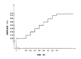
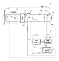
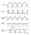
- the circuit block diagram of the non-contact electric power supply equipment in embodiment of this invention The figure which shows the time change of the oscillation frequency of the power supply device of the non-contact electric power supply equipment. The figure which shows the relationship between the oscillation frequency of the power supply device of the non-contact electric power supply equipment, and the electric power supplied to a moving body.
- FIG. 1 is a circuit configuration diagram of a contactless power supply facility according to an embodiment of the present invention.
- a high-frequency current is supplied from the power supply device 12 to the induction line 14, and a plurality of transport carts (an example of a device or an apparatus) 17 are contactless from the induction line 14 to which the high-frequency current is supplied. Power is being supplied.
- the guide line 14 is continuously laid (arranged) along a traveling rail (an example of a movement path; not shown) of the transport carriage 17.
- a capacitor 15 is connected to the induction line 14 in series, and a variable inductor 16 that adjusts the inductance value of the entire induction line 14 is connected in series.
- variable inductor 16 is connected when the line length of the induction line 14 is less than a predetermined length, that is, when the inductance value of the induction line 14 is less than a predetermined inductance value.
- a high frequency transformer 13 is interposed between the induction line 14 and the power supply device 12.
- the high-frequency transformer 13 is configured to amplify the output voltage when the distance (length) of the induction line 14 is long.
- the high-frequency transformer 13 is installed to amplify the output voltage up to twice.
- the transfer carriage 17 is provided with a pickup coil 51 that opposes the induction line 14 and in which an electromotive force is induced from the induction line 14, and a power receiving unit 27 is connected to the pickup coil 51.
- a load 58 for example, an inverter that controls an electric motor for traveling of the transport carriage 17
- whose power consumption fluctuates is connected to the power receiving unit 27.
- the power receiving unit 27 has a function of constant voltage control for controlling the output voltage to the load 58 at a constant level. For this reason, as shown in FIG. A capacitor (voltage capacitor) 56 is provided, and the output voltage to the load 58 is controlled to be constant by feeding back the voltage of the output capacitor 56.
- a resonance capacitor 52 that forms a resonance circuit 50 that resonates with the frequency of the high-frequency current flowing through the induction line 14 together with the pickup coil 51 is connected to the pickup coil 51 in parallel.
- the resonance frequency of the resonance circuit 50 is set to be 9.74 kHz.
- the power supply device 12 is connected to the commercial power supply 11, and includes a rectifier circuit 21 that converts an alternating current supplied from the commercial power supply 11 into a direct current, a start / stop circuit 22, a step-down circuit 23, an inverter 24, A controller 40 is provided.
- the controller 40 includes a main controller 41, a step-down controller 42, and a frequency / current controller 43, each of which includes a CPU (details will be described later). Further, the power supply device 12 is provided with a protection device (not shown) that detects whether the current flowing through the induction line 14 is an overcurrent (whether it is an overload). When the protection device detects an overload, the main controller 41 This interrupts the current supplied to the induction line 14 (described later).
- the start / stop circuit 22 includes an inrush resistor 31 and a coil (reactor) 32 that are connected in series between the rectifier circuit 21 and the step-down circuit 23, an activation conductor 33 that short-circuits the inrush resistor 31, and an inrush resistor 31.
- the discharge resistor 34 and the stop conductor 35 are connected in series between the connection point of the coil 32 and the rectifier circuit 21.
- the start conductor 33 and the stop conductor 35 are controlled to a connected state / open state by a main controller 41 described later. That is, the activation conductor 33 is opened when the power supply device 12 is activated, and the inrush current is suppressed by the inrush resistor 31. After a predetermined time from the activation, the activation conductor 33 is connected and the inrush resistor 31 is short-circuited. Further, the stop conductor 35 is opened during operation and is connected when stopped, and the electric charge accumulated in the power supply device 12 is consumed by the discharge resistor 34.
- Step-down circuit 23 is a step-down means for stepping down the DC voltage supplied to the inverter 24 according to the load of the induction line 14, and steps down the DC voltage input from the rectifier circuit 21 via the start / stop circuit 22.
- the step-down circuit 23 is driven and controlled by a step-down controller 42.
- the step-down controller 42 receives a first voltage mode command and a second voltage mode command from a main controller 41 described later, and drives the step-down circuit 23 according to the input mode command.
- the first voltage mode command is a mode command that outputs the direct current voltage input from the rectifier circuit 21 without being stepped down.
- the second voltage mode command is a mode command that realizes energy saving by stepping down to a predetermined voltage that can supply power normally consumed by the induction line 14.
- the DC voltage input from the rectifier circuit 21 is supplied as it is from the step-down circuit 23 to the inverter 24, and in the case of the second voltage mode command, the predetermined voltage stepped down from the step-down circuit 23 to the inverter 24. Is supplied.
- the inverter 24 converts the direct current output from the step-down circuit 23 into a high-frequency current having an arbitrary oscillation frequency and supplies it to the induction line 14.
- the inverter 24 includes a switching element 38 assembled in a full bridge. Each switching element 38 is driven by a pulse signal output from the frequency / current controller 43, converts a direct current input from the step-down circuit 23 into a high frequency alternating current, and supplies the induction line 14 as an output current.
- the frequency / current controller 43 receives the DC voltage and DC current input to the inverter 24 and the step-up ratio of the output voltage from the high-frequency transformer 13. Further, a target frequency of the oscillation frequency of the inverter 24 is input to the frequency / current controller 43 from a main controller 41 described later.
- the frequency / current controller 43 drives each switching element 38 so as to control the oscillation frequency of the inverter 24 to the target frequency input from the main controller 41, and at the same time, based on the input voltage / current and the step-up ratio of the inverter 24, the induction line
- Each switching element 38 is driven so that constant current control can be executed by calculating a current value flowing through the circuit 14 to obtain a predetermined duty ratio (pulse width) that becomes a constant current.
- the obtained duty ratio is output to the main controller 41.
- the main controller 41 has the following functions.
- Start / stop function Power supply start command from outside (command to normally start the power supply device 12), energy saving return command to return from energy saving operation, or intermittent operation to switch from OFF to ON when intermittent operation is performed
- start conductor 35 of the start / stop circuit 22 is opened, and then the start conductor 33 is connected.
- the stop conductor 35 is set in a connected state, and then the start conductor 33 is set in an open state.
- the voltage input from the commercial power supply 11 to the rectifier circuit 21 is monitored. When this voltage drops suddenly due to an instantaneous power failure or when the protective device detects an overload, the stop conductor of the start / stop circuit 22 is monitored. 35 is connected to shut off the power supply, and then the starting conductor 33 is opened. When the voltage is recovered from the instantaneous power failure, the stop conductor 35 of the start / stop circuit 22 is opened, and then the start conductor 33 is connected.
- Step-down function Normally, the second voltage mode command is output to the step-down controller 42. Further, it is confirmed whether or not the duty ratio input from the frequency / current controller 43 is approaching the maximum allowable duty ratio (for example, 80%), and if it is confirmed, the first voltage mode command is output to the step-down controller 42. When the input duty ratio is far from the maximum allowable duty ratio, the second voltage mode command is output to the step-down controller 42 again.
- the maximum allowable duty ratio for example, 80%
- the frequency / current controller 43 is supplied with the oscillation frequency of the inverter 24 at the start of power supply (input of a power supply start command, energy saving return command, intermittent operation / power supply start command, or recovery from an instantaneous power failure).
- start of power supply input of a power supply start command, energy saving return command, intermittent operation / power supply start command, or recovery from an instantaneous power failure.
- a low frequency shifted from the resonance frequency for example, 9.00 kHz (an example of a predetermined frequency) to a resonance frequency of 9.74 kHz, and output.
- the total power that can be taken out by all the carriages 17 by the resonance circuit 50 is set to a low frequency shifted from the resonance frequency so that it can be kept within the rated power that can be supplied by the power supply device 12.
- the predetermined frequency is swept from 9.00 kHz to the resonance frequency of 9.74 kHz. ing.
- the oscillation frequency of the inverter 24 is maintained at 9.00 kHz for 2 seconds (an example of the predetermined time) from the start of power feeding to the induction line 14, and subsequently, 9.10 kHz For 0.2 seconds, followed by 9.20 kHz for 0.2 seconds, followed by 9.30 kHz for 0.2 seconds, followed by 9.40 kHz for 0.2 seconds, Subsequently, 9.50 kHz is maintained for 0.2 seconds, subsequently, 9.60 kHz is maintained for 0.2 seconds, subsequently, 9.70 kHz is maintained for 0.2 seconds, and then 9.74 kHz (resonance frequency).
- the target frequency is output to the frequency / current controller 43 so as to maintain the output of).
- the inverter 24 When the inverter 24 starts power feeding from the power supply device 12 to the induction line 14 while performing constant current control by the action of the frequency / current controller 43 and the main controller 42, the inverter 24 changes the oscillation frequency from 9.00 kHz to 9.74 kHz. The sweep operation is being executed.
- the rated power (power that can be supplied) of the power supply device 12 is 30 kW
- the alternating current of the commercial power supply 11 is converted into a direct current by the rectifier circuit 21 and output to the start / stop circuit 22.
- the starting conductor 33 is in an open state and the stop conductor 35 is in a connected state, the inrush current at the time of activation is suppressed (limited) by the inrush resistor 31 and consumed by the discharge resistor 34.
- the starting conductor 43 is connected, the inrush resistor 31 is short-circuited, and then the stop conductor 35 is opened, and a stable DC current from which the inrush current has been eliminated is output to the step-down circuit 23.
- the DC voltage after rectification by the rectifier circuit 21 is DC 270V.
- the target frequency of the oscillation frequency by the inverter 24 is set to 9.00 kHz, and after a predetermined time (2 seconds), it is swept from 9.00 kHz to 9.74 kHz.
- the oscillation frequency is 9.00 kHz
- the current that can be taken out by the resonance circuit 50 of the transport carriage 17 is reduced.
- the rated power (1800 W) can be taken out at 9.74 kHz, while only 1200 W can be taken out at 9.00 kHz because of deviation from the resonance frequency of 9.74 kHz.
- the conveyance carriage 17 can be in a full load state, but after the predetermined time (2 seconds), the output voltage of each conveyance carriage 17 rises to the reference voltage. Therefore, the normal conveyance carriage 17 is in a state of receiving only the electric power consumed by the load 58, and there is no situation where all the conveyance carriages 17 take out electric power in the full load state all at once. . Further, even if there is a transport carriage 17 whose rise to the reference voltage is delayed and an attempt is made to take power in a full load state, it is limited to only a part of the transport carriage 17. Therefore, the power supply device 12 is not overloaded, and the power supply from the power supply device 12 to the induction line 14 is stably performed.
- the stop conductor 35 When stopping, the stop conductor 35 is connected, the start conductor 33 is opened, and the stop conductor 35 is connected. As a result, the charge accumulated in the power supply device 12 by the discharge resistor 34 is reduced. Is consumed.
- the oscillation frequency of the inverter 24 is made lower than 9.00 kHz, the power that can be taken out by the transport carriage 17 is further reduced, so that the time until the output voltage of the power receiving unit 27 rises to the reference voltage becomes longer. .
- the power receiving unit 27 includes the resonant capacitor 52 and a rectifier circuit (full-wave rectifier circuit) 53 connected to the resonant capacitor 52.
- the power receiving unit 27 includes a choke coil 54, a diode 55, the output capacitor (voltage capacitor) 56, a switch means (for example, an output adjustment transistor) 57, and a controller (control device) 61 as a constant voltage control circuit. It has.
- the choke coil 54 has one end connected to a positive output terminal (one output terminal) 53a of the rectifier circuit 53.
- the anode of the diode 55 is connected to the other end of the choke coil 54.
- the output capacitor 56 has one end connected to the cathode of the diode 55 and the other end connected to the negative output terminal (the other output terminal) 53 b of the rectifier circuit 53.
- the switch means 57 has one end connected to the connection point between the other end of the choke coil 54 and the anode of the diode 55, and the other end connected to the negative output terminal 53 b of the rectifier circuit 53.
- the controller 61 places the switch means 57 in a connected state (switch means is on) or an open state (switch means is off).
- the load 58 is connected between circuit output terminals 59a and 59b connected to both ends of the output capacitor 56.
- the controller 61 receives a full-wave input voltage (full-wave input voltage signal) V 1 of the choke coil 54 that is a voltage immediately after rectification output to the plus-side output terminal 53a of the full-wave rectifier circuit 53 as a control signal. There is an input, an output voltage (voltage across the output capacitor 56, the voltage of the load 58) of the circuit V 2 is input as a feedback signal. Further, the controller 61 outputs a drive pulse P 2 to the switch means 57.
- the controller 61 includes a gate pulse oscillator (an example of a pulse generation circuit) 62, a PWM module (an example of a pulse width control circuit) 63, and a control power supply device 64.
- Control power supply 64 The control power supply device 64 supplies the control power supply (predetermined voltage V 3 ) to the gate pulse oscillator 62 and the PWM module 63 using the output voltage (the voltage across the output capacitor 56 and the voltage of the load 58) V 2 as an input power supply. (Voltage across the output capacitor 56, the voltage of the load 58) the output voltage V 2 is at startup is 0V, the output voltage V 2 rises to a predetermined voltage (e.g., 15V), controlled by the predetermined voltage V 3 The power supply can be supplied.
- a predetermined voltage e.g. 15V
- the gate pulse oscillator 62 is synchronized with the full-wave input voltage V 1 of the choke coil 54 output to the plus-side output terminal 53 a of the full-wave rectifier circuit 53 when the control power is supplied from the control power supply device 64.
- 6 is a pulse generation circuit that outputs a synchronization pulse (trigger) having a frequency (2f) that is twice (an example of a plurality of times) the frequency f of the high-frequency current of the induction line 14, and the input voltage V of the choke coil 54 shown in FIG. 1 is output to the PWM module 63 as a switch triggered by forming a synchronization pulse P 1 for each zero voltage.
- Input voltages V 1 since the output voltage of the full-wave rectifier circuit 53, has a continuous waveform of a frequency 2f, synchronous pulses P 1 of the frequency 2f is outputted.
- PWM module 63 receives the output voltage V 2 and the synchronization pulse P 1 output from the gate pulse oscillator 62. PWM module 63, the control power is supplied from the control power supply unit 64, and outputs a driving pulse P 2 to the switch unit 57, the driving pulse P 2 is a switch means 57 when on the connection state, when the off switch This is a pulse width control circuit that opens the means 57, and is configured as shown in FIG.
- the PWM module 63 includes a first comparator 71, a second comparator 72, a third comparator 73, a timer 74, an RS flip-flop 75, a pulse width calculator 77, A pulse driving unit 78 and the like are provided.
- the first comparator 71 whether the control power is supplied, that is, the voltage V 3 of the control power supply to determine whether a predetermined voltage (e.g., 15V) or more.
- the second comparator 72, the output voltage V 2 is the reference voltage (e.g., 310 V) to determine whether more.
- the third comparator 73, the output voltage V 2 is set voltage (e.g., 100 V) to determine whether more.
- the timer 74 starts counting in response to an output signal of the first comparator 71, that is, a start signal output when the control power is supplied (started up). For example, 5 seconds).
- the RS flip-flop 75 is set when a signal (elapsed signal) output when the timer 74 counts up is on, or when the start signal is on and the output signal of the second comparator 72 is on, It is reset when the activation signal is turned off.
- a relay RY1 that is operated (excited) when the RS flip-flop 75 is set is provided. Also provided is a relay RY2 that is activated (excited) when the start signal is on, the output signal of the relay RY1 is off (b contact is connected), and the output signal of the second comparator 72 is off. Yes. Also, a relay RY3 is provided that operates (excited) when the output signal (contact a) of the relay RY1 is on and the output signal of the third comparator 73 is off.
- the relay RY1 when is started the supply of the high frequency current I to the inductive line 14 (start signal is ON), and the output voltage V 2 is the reference voltage (e.g., the 310 V) equal to or greater than a (second 2 when the output signal of the comparator 72 is ON) or when a set time (scheduled time, for example, 5 seconds) has elapsed (the output signal of the timer 74 is ON). That is, it operates when the initial state is shifted to the normal state.
- start signal is ON
- the output voltage V 2 is the reference voltage (e.g., the 310 V) equal to or greater than a (second 2 when the output signal of the comparator 72 is ON) or when a set time (scheduled time, for example, 5 seconds) has elapsed (the output signal of the timer 74 is ON). That is, it operates when the initial state is shifted to the normal state.
- the relay RY2 is induced line 14 supplies high-frequency current I is started to (start signal is ON), and the output voltage V 2 is the reference voltage (e.g., 310 V) than when (output signal of the second comparator 72 Is turned off), that is, operates in the initial state, and when it shifts to the normal state (when the relay RY1 operates), it becomes inoperative.
- the relay RY3 is (the normal state) when the relay RY1 is operating, the output voltage V 2 is set voltage (e.g., 100 V) operating with abnormally lowered to less than.
- the pulse width calculating section 77, the output voltage V 2 and the synchronous pulses P 1 is input, the pulse width calculating section 77, a reference voltage as the target voltage to perform the output voltage feedback control.
- the pulse width calculation unit 77 forms a PWM reference wave (triangular wave) in synchronization with the synchronization pulse P 1 having the frequency 2f input from the gate pulse oscillator 62, that is, the input of the choke coil 54. forming a triangle wave with a peak position peak of the input voltages V 1 in synchronization with the voltages V 1. Then, the pulse width calculation unit 77 presets a reference voltage (indicated by a one-dot chain line) of the output voltage V 2 that intersects this triangular wave, and determines the position where the input voltage V 1 of the choke coil 54 has changed from a peak to a drop.
- a reference voltage indicated by a one-dot chain line
- the driving pulse P 2 and the on-timing, the triangular wave than the reference voltage (voltage) is the going on time pulse width of the drive pulse P 2 lower.
- the output voltage V 2 matches the reference voltage
- the time of the triangular wave when the triangular wave voltage is lower than the reference voltage is set as the “reference pulse width” of the drive pulse P 2
- the load 58 is the rated load.
- the drive pulse P 2 of the reference pulse width is output, the output voltage V 2 is maintained at the reference voltage.
- the triangular wave thereby obtaining a pulse width of the drive pulse P 2 by crossing the output voltage V 2 input.
- the pulse width of the drive pulse P 2 when the output voltage V 2 is lower than the reference voltage shorter than the "reference pulse width” as shown in FIG. 7, the driving pulse P 2 is higher than the reference voltage Is made longer than the “reference pulse width”, and a duty ratio is obtained and output to the pulse driver 78.
- the pulse driver 78 outputs a pulse to the switch means 57.
- the pulse drive section 78 is synchronized pulse P 1 is input, and (when the initial state) output signal of the relay RY2 (a contact) is When on, or when the output signal of the relay RY3 (a contact) is on (output when the voltage V 2 dropped abnormally), pre-set duty ratio (hereinafter, referred to as the fixed duty ratio, for example, 50%) is input, when the output signal of the relay RY1 (a contact) is on The duty ratio output from the pulse width calculation unit 77 is input.
- Pulse driving unit 78 forms a driving pulse P 2 on the basis of the duty ratio input, and outputs to the switch means 57 the midpoint of the driving pulse P 2 as the zero-cross position of the input voltage V 1 of the full-wave, pulse width control Is running.
- the fixed duty ratio is obtained as follows. First, the rated power of the power supply device 12 is divided by the number of conveyance carts 17 (an example of equipment or devices) to be fed, and the received power that can be received per unit is obtained when feeding to the induction line 14 is started. .
- the pulse width m is set so that the above-obtained “received power that can be received per unit” is suppressed.
- the power supply device 12 that feeds the high-frequency current to the induction line 14 is in a 1/2 load state (50% load state) even when all the carriages 17 simultaneously take a load at the start of feeding. Therefore, the power supply device 12 will not be overloaded, and the situation where power feeding stops can be avoided.
- a synchronization pulse input voltage V 1 is the timing of the position of the on-driving pulse P 2 having turned down from the peak of P 1 in synchronization with the choke coil 54 of the frequency 2f, the drive pulse the midpoint of pulse width of P 2 as the zero-cross position of the input voltage V 1 of the full-wave, high-speed switching is performed by switching frequency 2f.
- the output voltage V 2 is the reference voltage or more, or when the timer 74 is counted up, the duty ratio output from the pulse width calculating section 77
- high-speed switching is executed, that is, output voltage feedback control with the reference voltage as the target voltage is executed.
- the load 58 is reduced, the output voltage V 2 is increased, and when the output voltage V 2 exceeds a preset reference voltage, the driving is output to the switch means 57.
- the output voltage V 2 is less than the set voltage (the relay RY3 is turned on), with 50% fixed duty ratio, high speed Switching is performed.
- the output capacitor 56 is in an empty state, the output voltage V 2 is 0V.
- PWM module 63 can not output the driving pulse P 2 Therefore, the switch means 57 is in an open state, and the output capacitor 56 is continuously charged by the current output from the full-wave rectifier circuit 53.
- the current is added to the excitation energy of the choke coil 54 to charge the output capacitor 56 and is supplied to the load 58 at the same time.
- the switch means 57 is in the connected state, while the energy choke coil 54 is excited is filled by current output from the full-wave rectifier circuit 53, from the output capacitor 56 A discharge current is supplied to the load 58.
- the frequency of the current flowing through the induction line 14 is 9.00 kHz, which is deviated from the resonance frequency of the resonance circuit 50, so that only 1200 W can be taken out in the full load state and 1/2 load In this state, only 600 W can be taken out.
- the switch unit 57 is a high speed switching at the switching frequency 2f
- the pulse width of the drive pulse P 2 is determined by the output voltage V 2 at the time of pulse-on timing is lower than the reference voltage the output voltage V 2 is set in advance
- the load 58 decreases, the voltage across the output capacitor 56, that is, the output voltage V 2 increases and the output voltage V 2 exceeds the reference voltage, the longer it takes for the switching means 57 are in a connected state , the output voltage V 2 is maintained at lowered by the reference voltage.
- the load 58 is increased, the voltage across the output capacitor 56, i.e., lowered output voltage V 2, when the output voltage V 2 drops below the reference voltage, the longer it takes for the switching means 57 is opened, the output voltage V 2 is maintained at a raised by the reference voltage.
- the on-timing of the driving pulse P 2 by the input voltage V 1 of the choke coil 54 is set to a position turned to the lowered from the peak, the driving pulse P 2 is turned on, i.e., the choke coil 54 Is energized, the current supplied to the choke coil 54 by the resonant circuit 50 is 90 ° out of phase, so this current is approximately zero, and thereafter the input voltage V 1 drops, by input voltages V 1 is the range in which zero cross, elevated current (coil current) I 1 flowing through the choke coil 54 is suppressed, (less pulsation) to smooth made. Also as this, the pulsation of the coil current I 1 is reduced, by the difference between the input voltage and the output voltage of the choke coil 54 is reduced, the ripple of the coil current I 1 is suppressed greatly.
- the high-speed switching at the switching frequency 2f quickly responds to the fluctuation of the load 58, and the influence of the fluctuation of the load 58 on the induction line 14 via the resonance circuit 50, for example, the feedback impedance suddenly becomes zero. By being close to each other, the influence that the induction line 14 becomes an overcurrent is suppressed.
- the power supply can be maintained. That is, the power feeding frequency characteristics are improved as compared with the conventional case, and power can be obtained in a wide frequency shift range, and power can be supplied stably even if the frequency of the high-frequency current is shifted.
- the duty ratio of 0% i.e. the switch means 57 is opened, the state of full load, the output capacitor 56 to a reference voltage and maximum charging Try to return. Nevertheless, without increasing the output voltage V 2, drops to a set voltage, it is determined that abnormal supply of the current flowing in the induction line 14 side is generated, so that the induction line 14 side not to load 1 ⁇ 2 load state.
- one power supply device 12 restricts the transfer carriage 17 from taking in the frequency of the high-frequency current flowing through the induction line 14 as a frequency shifted from the resonance frequency.
- the loading is limited as a load state, avoiding the situation where the power supply device 12 is overloaded and the high-frequency current flowing through the induction line 14 is cut off and power supply cannot be performed.
- the power supply device 12 is overloaded and flows through the induction line 14 only by setting the frequency of the high-frequency current that the power supply device 12 flows through the induction line 14 to a frequency shifted from the resonance frequency. A situation in which the high frequency current is interrupted and power supply cannot be performed is avoided.
- the oscillation frequency of the inverter 24 of the power supply device 12 is set to the resonance frequency of the resonance circuit 50 of each conveyance carriage 17.
- the frequency is 9.00 kHz, which is a predetermined frequency shifted from 9.74 kHz, even if all the transport carriages 17 try to take power from the induction line 14 connected to the power supply device 12 in the full load state, all the transport carriages 17 Therefore, it is possible to suppress the total power to be taken within the power that can be supplied by the power supply device 12 and to prevent the power supply device 12 from being overloaded.
- each normal transport carriage 17 only takes out the power consumed by the load 58 such as the travel motor of each transport carriage 17. There is no situation in which the transport carriage 17 takes out electric power all at once in a full load state.
- the oscillation frequency of the inverter 24 of the power supply device 12 is continuously or stepwise increased from the predetermined frequency of 9.00 kHz to the resonance frequency of 9.74 kHz, thereby causing the power supply device 12 to increase. It is possible to avoid a sudden load on the inverter 24. Further, by setting the resonance frequency of the resonance circuit 50 of the transport carriage 17 to 9.74 kHz, which is less than 10 kHz, and to set the predetermined frequency to 9.00 kHz, which is a frequency lower than the resonance frequency, the frequency band to be used is 9. kHz, which is less than 10 kHz.
- the power capacity of the power supply device 12 is changed while changing the duty ratio of the switch means 57 in accordance with the load 58 whose power consumption fluctuates when each transport carriage 17 is operating normally.
- the oscillation frequency of the inverter 24 of the power supply device 12 is equal to 9.74 kHz, which is the resonance frequency of the resonance circuit 50 of the transport carriage 17, as in the start-up when power supply from the power supply device 12 to the induction line 14 is started.
- the power supply device 12 In the resonance state, the power supply device 12 has an appropriate power capacity by being smaller than the total power taken out in the full load state, and can suppress an increase in equipment cost.
- the oscillation frequency of the inverter 24 is controlled so as to change stepwise from a predetermined frequency of 9.00 kHz, which is lower than the resonance frequency of 9.74 kHz, to a resonance frequency of 9.74 kHz. ing.
- the oscillation frequency of the inverter 24 may be controlled stepwise from a frequency (for example, 10.5 kHz) higher than the resonance frequency (9.74 kHz) to the resonance frequency (9.74 kHz).
- the oscillation frequency of the inverter 24 is changed stepwise toward the resonance frequency in increments of 0.1 kHz, but the interval of the increments is set to be greater than 0.1 kHz regardless of the increment of 0.1 kHz.
- the frequency may be increased, or it may be smaller than 0.1 kHz and the frequency may be continuously changed.
- the PWM module 63 of the controller 61 forms the PWM reference wave (triangular wave) in synchronization with the synchronization pulse P 1 having the frequency 2f input from the gate pulse oscillator 62.
- the synchronization pulse P 1 in two waveforms synchronous to the input voltages V 1 to every other, three PWM reference wave (triangular wave) to form, a rise of the triangular wave may be a timing of turning on the driving pulse P 2.
- the switching frequency of the drive pulse P 2 is 3 times (3f) next to the high-frequency current frequency f, are switched faster.
- the fluctuation of the load 58 is more quickly dealt with, and the influence of the fluctuation of the load 58 on the induction line 14 via the resonance circuit 50, for example, the induction impedance 14 becomes excessive due to a sudden return impedance close to zero.
- the influence of current can be suppressed.
- the output voltage V 2 faster is corresponding, it is possible to suppress the resonance voltage increases rapidly.
- the transport carriage 17 has been described as an example of the device or device.
- the device or device includes a self-propelled vehicle or a stationary device / device that does not have a transport function.
Landscapes
- Engineering & Computer Science (AREA)
- Power Engineering (AREA)
- Transportation (AREA)
- Mechanical Engineering (AREA)
- Life Sciences & Earth Sciences (AREA)
- Sustainable Development (AREA)
- Sustainable Energy (AREA)
- Computer Networks & Wireless Communication (AREA)
- Current-Collector Devices For Electrically Propelled Vehicles (AREA)
- Inverter Devices (AREA)
Abstract
Description
この電源装置は、交流電圧が変動する交流電源(商用電源)の交流電流を直流電流に変換する整流器と、誘導線路の負荷に応じて前記整流器の出力電圧(直流電圧)を昇降圧する昇降圧回路と、インバータから構成されている。
前記インバータは、PWM制御により前記誘導線路に流れる電流が一定となるようにそれぞれ駆動される複数のスイッチング素子により、前記昇降圧回路により昇降圧された直流電流を前記所定周波数の一定交流電流に変換して前記誘導線路に出力電流として給電する。
この2次側受電回路は、受電コイルに受電コイルとともに誘導線路の周波数に共振する共振回路を形成する共振コンデンサを接続し、この共振コンデンサに整流回路を接続し、さらに整流回路に、出力電圧を基準電圧に制御する定電圧制御回路を接続して構成され、負荷はこの定電圧制御回路に接続され、共振状態で、この定電圧制御回路より負荷へ給電している。
誘導線路に高周波電流が供給される以前の初期状態では、各移動体の定電圧制御回路の出力電圧(出力コンデンサの電圧)は0Vであり、誘導線路へ高周波電流の供給が開始されると、各移動体の定電圧制御回路は、スイッチ手段を連続して開放状態にする全負荷状態として出力コンデンサを充電することにより、出力電圧を基準電圧に上昇させる制御を開始する。このように、初期状態から誘導線路へ高周波電流の供給が開始されると、全移動体が全負荷状態で受電しようとするために、電源装置が過負荷状態となり、電源装置の保護機能が働いて誘導線路への給電が遮断されてしまい、全て移動体が停止するという事態が発生する。これは、電源装置から誘導線路へ供給できる電力の容量を、全移動体の出力コンデンサが充電された状態で(定電圧となっている状態で)、各移動体の負荷が消費する電力(通常の負荷状態の電力)を給電できる容量としていることにより発生する。また、この通常の負荷状態の電力を超える電力の容量を電源装置に要求すると、通常必要としない電力を供給できる電源装置となってしまい、高価な装置となってしまう。
前記各機器または装置に、前記誘導線路に対向して前記誘導線路より起電力が誘起されるピックアップコイルと、前記ピックアップコイルに並列に接続され、このピックアップコイルと共に前記高周波電流の周波数に共振する共振回路を形成する共振コンデンサと、前記共振回路の共振コンデンサに並列に接続された全波整流回路と、前記全波整流回路の出力端子間に並列に接続された、スイッチ、および消費電力が変動する負荷に電力を供給する出力コンデンサと、前記スイッチの接続状態と開放状態とを切換えることにより、前記出力コンデンサの電圧を一定の基準電圧に制御するコントローラを備え、前記電源装置は、商用電源から供給される交流電流を直流電流に変換する整流回路と、前記直流電流を任意の発振周波数の高周波電流に変換し、前記誘導線路に供給するインバータと、前記電源装置から誘導線路への給電を開始するときに、前記電源装置のインバータの発振周波数を、前記共振回路により全ての機器または装置が取り出すことができる総電力を前記電源装置が供給できる電力内に抑えるよう、前記共振回路が共振する周波数よりずらした所定周波数とし、誘導線路への給電により前記各機器または装置の出力コンデンサの出力電圧が、基準電圧まで上昇可能な所定時間の経過後、前記所定周波数から前記共振周波数へ変化させるコントローラを備えることを特徴とするものである。
この無接触給電設備では、電源装置12より誘導線路14へ高周波電流を給電し、この高周波電流が給電される誘導線路14より複数台の搬送台車(機器または装置の一例)17にそれぞれ無接触で給電している。前記誘導線路14は搬送台車17の走行レール(移動経路の一例;図示せず)に沿って連続して敷設(配置)されている。誘導線路14にはコンデンサ15が直列に接続され、さらに誘導線路14全体のインダクタンス値を調整する可変インダクタ16が直列に接続されている。この可変インダクタ16は、誘導線路14の線路長が所定の長さに満たないとき、すなわち誘導線路14のインダクタンス値が所定のインダクタンス値に満たないときに接続される。またこの誘導線路14と電源装置12との間に高周波トランス13が介装されている。この高周波トランス13は、誘導線路14の距離(長さ)が長いときに出力電圧を増幅することができるようにされ、例えば出力電圧を2倍まで増幅することができるように設置されている。
電源装置12は、商用電源11に接続されており、商用電源11から供給される交流電流を直流電流に変換する整流回路21と、起動・停止回路22と、降圧回路23と、インバータ24と、コントローラ40を備えている。
前記起動・停止回路22は、整流回路21と降圧回路23との間に直列に接続される突入抵抗31およびコイル(リアクトル)32と、前記突入抵抗31を短絡する起動コンダクタ33と、突入抵抗31およびコイル32の接続点と整流回路21との間に直列に接続されている放電抵抗34および停止コンダクタ35から構成されている。
前記降圧回路23は、誘導線路14の負荷に応じてインバータ24へ供給する直流電圧を降圧する降圧手段であり、整流回路21より起動・停止回路22を介して入力した直流電圧を降圧する。降圧回路23は、降圧コントローラ42により駆動・制御される。降圧コントローラ42には、後述するメインコントローラ41より、第1電圧モード指令と第2電圧モード指令が入力され、入力されたモード指令にしたがって降圧回路23を駆動する。
前記インバータ24は、降圧回路23から出力された直流電流を任意の発振周波数の高周波電流に変換し、誘導線路14に供給する。
インバータ24は、フルブリッジに組まれたスイッチング素子38から構成されている。各スイッチング素子38は、周波数・電流コントローラ43より出力されるパルス信号により駆動され、降圧回路23から入力する直流電流を高周波の交流電流に変換して誘導線路14に出力電流として給電する。
メインコントローラ41は、以下の機能を有している。
外部から給電開始指令(電源装置12を普通に起動する指令)、または省エネ運転から復帰する省エネ復帰指令、または間欠運転をするときにオフ状態からオン状態とする間欠運転・給電開始指令を入力すると、起動・停止回路22の停止コンダクタ35を開放状態にし、続いて起動コンダクタ33を接続状態とする。また停止時には、停止コンダクタ35を接続状態にし、続いて起動コンダクタ33を開放状態とする。
通常は上記第2電圧モード指令を降圧コントローラ42へ出力している。また周波数・電流コントローラ43より入力するデューティ比が、最大許容デューティ比(例えば、80%)に近づいているかどうかを確認し、確認すると第1電圧モード指令を降圧コントローラ42に出力する。また入力したデューティ比が最大許容デューティ比より遠のくと、再び第2電圧モード指令を降圧コントローラ42へ出力する。
給電開始時(給電開始指令または省エネ復帰指令または間欠運転・給電開始指令の入力時、あるいは瞬停からの復帰時)に、周波数・電流コントローラ43に、インバータ24の発振周波数の目標周波数を、共振周波数からずらした低い周波数、例えば9.00kHz(所定周波数の一例)から共振周波数の9.74kHzまでスイープさせて出力する。
上記電源装置12の構成における作用を説明する。
図4に示すように、受電ユニット27は、前記共振コンデンサ52と、この共振コンデンサ52に接続される整流回路(全波整流回路)53とを備えている。
制御電源装置64は、出力電圧(出力コンデンサ56の両端電圧、負荷58の電圧)V2を入力電源として、制御電源(所定電圧V3)をゲートパルス発振器62とPWMモジュール63へ供給する。前記出力電圧(出力コンデンサ56の両端電圧、負荷58の電圧)V2は、起動時は0Vであり、出力電圧V2が所定の電圧(例えば、15V)まで上昇すると、所定電圧V3で制御電源を供給可能な構成とされている。
前記ゲートパルス発振器62は、制御電源装置64より制御電源が供給されると、全波整流回路53のプラス側出力端子53aに出力されるチョークコイル54の全波の入力電圧V1に同期して、誘導線路14の高周波電流の周波数fの2倍(複数倍の一例)の周波数(2f)の同期パルス(トリガ)を出力するパルス発生回路であり、図6に示すチョークコイル54の入力電圧V1がゼロ電圧となる毎に同期パルスP1を形成しスイッチトリガーとしてPWMモジュール63へ出力している。入力電圧V1は、全波整流回路53の出力電圧であるから、周波数2fの連続波形となっており、周波数2fの同期パルスP1が出力される。
前記PWMモジュール63には、出力電圧V2と、ゲートパルス発振器62から出力された同期パルスP1が入力されている。PWMモジュール63は、制御電源装置64から制御電源が供給されると、スイッチ手段57へ駆動パルスP2を出力し、駆動パルスP2がオンのときスイッチ手段57を接続状態とし、オフのときスイッチ手段57を開放状態とするパルス幅制御回路であり、図5に示すように、構成されている。
まず、電源装置12の定格電力を、給電対象の搬送台車(機器または装置の一例)17の台数で除算して、誘導線路14への給電開始時に、1台当たりに受電可能な受電電力を求める。
この受電電力以内に抑制可能な駆動パルスP2のパルス幅mを、出力可能な駆動パルスのパルス幅Wより除算することにより、固定デューティ比(=m/W)で求めている。本実施の形態では、50%としている。
上記受電ユニット27の構成における作用を説明する。
起動前には、出力コンデンサ56が空の状態にあり、出力電圧V2は0Vである。そして、誘導線路14へ高周波電流Iの供給が開始されると、その直後は、制御電源装置64から制御電源を供給できない状態であり、このとき、PWMモジュール63は、駆動パルスP2を出力できないためスイッチ手段57は開放状態となっており、全波整流回路53から出力された電流により、出力コンデンサ56が連続して充電される。
出力コンデンサ56が充電され、出力電圧V2が上昇し、制御電源装置64から制御電源を供給できる状態となると、ゲートパルス発振器62から同期パルスP1がPWMモジュール63へ入力され、またPWMモジュール63では、制御電源の確認により起動信号がオンとなり、タイマー74が駆動され、このとき出力電圧V2は基準電圧未満であるので、固定デューティ比50%に制限され、すなわち1/2負荷の状態で高速スイッチングが実行される。
タイマー74がカウントアップすると、強制的に、あるいは出力電圧V2は基準電圧以上となると、基準電圧を目標電圧とし出力電圧フィードバック制御が実行される。パルス幅演算部77から出力されたデューティ比で、高速スイッチングが実行される。
出力電圧フィードバック制御の実行中に、出力電圧V2が設定電圧未満まで低下すると、デューティ比は、固定デューティ比50%に制限され、すなわち1/2負荷の状態で、高速スイッチングが実行される。
Claims (3)
- 電源装置(12)より誘導線路(14)へ高周波電流を給電し、この高周波電流が給電される誘導線路(14)より複数の機器または装置(17)にそれぞれに無接触で給電する無接触給電設備であって、
前記各機器または装置(17)に、
前記誘導線路(14)に対向して前記誘導線路(14)より起電力が誘起されるピックアップコイル(51)と、
前記ピックアップコイル(51)に並列に接続され、このピックアップコイル(51)と共に前記高周波電流の周波数に共振する共振回路(50)を形成する共振コンデンサ(52)と、
前記共振回路(50)の共振コンデンサ(52)に並列に接続された全波整流回路(53)と、
前記全波整流回路(53)の出力端子間に並列に接続された、スイッチ(57)、および消費電力が変動する負荷に電力を供給する出力コンデンサ(56)と、
前記スイッチ(57)の接続状態と開放状態とを切換えることにより、前記出力コンデンサ(56)の電圧を一定の基準電圧に制御するコントローラ(61)
を備え、
前記電源装置(12)は、
商用電源から供給される交流電流を直流電流に変換する整流回路(21)と、
前記直流電流を任意の発振周波数の高周波電流に変換し、前記誘導線路(14)に供給するインバータ(24)と、
前記電源装置(12)から誘導線路(14)への給電を開始するときに、前記電源装置(12)のインバータ(24)の発振周波数を、前記共振回路(50)により全ての機器または装置(17)が取り出すことができる総電力を前記電源装置(12)が供給できる電力内に抑えるよう、前記共振回路(50)が共振する周波数よりずらした所定周波数とし、誘導線路(14)への給電により前記各機器または装置(17)の出力コンデンサ(56)の出力電圧が、基準電圧まで上昇可能な所定時間の経過後、前記所定周波数から前記共振周波数へ変化させるコントローラ(40)
を備えること
を特徴とする。 - 特許請求範囲第1項記載の無接触給電設備であって、
前記共振回路(50)の共振周波数を10kHz未満に設定し、
前記コントローラ(40)は、前記所定周波数を前記共振周波数よりも低い周波数とし、前記インバータ(24)の発振周波数を前記所定周波数から前記共振周波数へ連続的または段階的に上昇させること
を特徴とする。 - 特許請求範囲第1項または請求項2に記載の無接触給電設備であって、
前記電源装置(12)が供給できる電力の容量を、全ての機器または装置(17)の共振回路(50)が、共振状態で、消費電力が変動する負荷に合わせて取りだす総電力より大きく、全ての機器または装置(17)の共振回路(50)が、共振状態で、全負荷状態で取りだす総電力より小さく設定したこと
を特徴とする。
Priority Applications (3)
| Application Number | Priority Date | Filing Date | Title |
|---|---|---|---|
| CN201280004565.6A CN103283121B (zh) | 2011-03-16 | 2012-03-08 | 非接触供电设备 |
| KR1020137016939A KR101802895B1 (ko) | 2011-03-16 | 2012-03-08 | 무접촉 급전 설비 |
| US14/002,759 US9362048B2 (en) | 2011-03-16 | 2012-03-08 | Contactless power feed equipment |
Applications Claiming Priority (2)
| Application Number | Priority Date | Filing Date | Title |
|---|---|---|---|
| JP2011-057324 | 2011-03-16 | ||
| JP2011057324A JP5488505B2 (ja) | 2011-03-16 | 2011-03-16 | 無接触給電設備 |
Publications (1)
| Publication Number | Publication Date |
|---|---|
| WO2012124580A1 true WO2012124580A1 (ja) | 2012-09-20 |
Family
ID=46830653
Family Applications (1)
| Application Number | Title | Priority Date | Filing Date |
|---|---|---|---|
| PCT/JP2012/055898 Ceased WO2012124580A1 (ja) | 2011-03-16 | 2012-03-08 | 無接触給電設備 |
Country Status (6)
| Country | Link |
|---|---|
| US (1) | US9362048B2 (ja) |
| JP (1) | JP5488505B2 (ja) |
| KR (1) | KR101802895B1 (ja) |
| CN (1) | CN103283121B (ja) |
| TW (1) | TWI515990B (ja) |
| WO (1) | WO2012124580A1 (ja) |
Cited By (1)
| Publication number | Priority date | Publication date | Assignee | Title |
|---|---|---|---|---|
| WO2015032525A1 (de) * | 2013-09-06 | 2015-03-12 | Robert Bosch Gmbh | Vorrichtung zur induktiven energieübertragung und verfahren zur induktiven energieübertragung |
Families Citing this family (22)
| Publication number | Priority date | Publication date | Assignee | Title |
|---|---|---|---|---|
| KR101896921B1 (ko) * | 2011-05-17 | 2018-09-12 | 삼성전자주식회사 | 무선 전력 수신기 및 그 제어 방법 |
| GB2502055A (en) | 2012-05-14 | 2013-11-20 | Nicoventures Holdings Ltd | Modular electronic smoking device |
| JP2014030288A (ja) * | 2012-07-31 | 2014-02-13 | Sony Corp | 給電装置および給電システム |
| GB2507104A (en) | 2012-10-19 | 2014-04-23 | Nicoventures Holdings Ltd | Electronic inhalation device |
| EP3054574B1 (en) * | 2013-09-30 | 2020-03-11 | Mitsubishi Electric Corporation | Power conversion device and air conditioner using same |
| GB2519101A (en) * | 2013-10-09 | 2015-04-15 | Nicoventures Holdings Ltd | Electronic vapour provision system |
| DE102014209501A1 (de) * | 2014-05-20 | 2015-11-26 | Siemens Aktiengesellschaft | Anordnung, System und Verfahren zum induktiven Übertragen von Energie für das Laden mindestens eines Energiespeichers eines Schienenfahrzeugs |
| JP6497614B2 (ja) | 2014-05-26 | 2019-04-10 | パナソニックIpマネジメント株式会社 | 送電装置及び無線電力伝送システム |
| JP6384779B2 (ja) * | 2014-06-13 | 2018-09-05 | パナソニックIpマネジメント株式会社 | 非接触給電システム |
| JP2016226088A (ja) * | 2015-05-27 | 2016-12-28 | エスアイアイ・セミコンダクタ株式会社 | 給電システム |
| JP5964488B1 (ja) * | 2015-07-31 | 2016-08-03 | ファナック株式会社 | 保護動作制御部を有するモータ制御装置、ならびに機械学習装置およびその方法 |
| WO2017068628A1 (ja) | 2015-10-19 | 2017-04-27 | 三菱電機株式会社 | 空気調和機 |
| WO2017178967A1 (fr) * | 2016-04-12 | 2017-10-19 | Mobisystems Sa | Dispositif de sécurité pour la transmission d'énergie sans contact par induction magnétique |
| JP6747163B2 (ja) * | 2016-08-15 | 2020-08-26 | 株式会社リコー | 電源装置 |
| CN106549457B (zh) * | 2016-12-27 | 2019-01-11 | 深圳大学 | 一种无线充电驱动芯片 |
| JP6965793B2 (ja) * | 2018-03-05 | 2021-11-10 | オムロン株式会社 | 非接触給電装置 |
| JP7208075B2 (ja) * | 2019-03-20 | 2023-01-18 | アズビル株式会社 | 周波数検出回路 |
| CN113270948B (zh) * | 2021-05-26 | 2022-09-23 | 重庆大学 | 抑制功率波动的动态无线充电系统及其参数设计方法 |
| JP7487720B2 (ja) * | 2021-11-05 | 2024-05-21 | 株式会社ダイフク | 非接触給電設備、非接触給電設備のインピーダンス調整方法、及び非接触給電設備のインピーダンス調整プログラム |
| CN114043882A (zh) * | 2021-11-16 | 2022-02-15 | 桔充充(杭州)新能源有限公司 | 一种适配于多种二轮电动车电池的无线充电系统 |
| JP7729285B2 (ja) * | 2022-08-09 | 2025-08-26 | 株式会社ダイフク | 電源装置 |
| DE102023103932A1 (de) * | 2023-02-17 | 2024-08-22 | Brusa Elektronik Ag | Vorrichtung für ein induktives Ladesystem sowie induktives Ladesystem |
Citations (4)
| Publication number | Priority date | Publication date | Assignee | Title |
|---|---|---|---|---|
| JP2000125487A (ja) * | 1998-10-13 | 2000-04-28 | Hitachi Kiden Kogyo Ltd | 非接触給電装置 |
| JP2005313884A (ja) * | 2004-03-30 | 2005-11-10 | Daifuku Co Ltd | 無接触給電設備 |
| JP2008206327A (ja) * | 2007-02-21 | 2008-09-04 | Seiko Epson Corp | 送電制御装置、受電制御装置、無接点電力伝送システム、送電装置、受電装置および電子機器 |
| JP2009268181A (ja) * | 2008-04-22 | 2009-11-12 | Olympus Corp | エネルギー供給装置 |
Family Cites Families (8)
| Publication number | Priority date | Publication date | Assignee | Title |
|---|---|---|---|---|
| JP3506006B2 (ja) | 1998-05-27 | 2004-03-15 | 株式会社ダイフク | 無接触給電設備の2次側受電回路 |
| JP2004282827A (ja) * | 2003-03-13 | 2004-10-07 | Honda Motor Co Ltd | 発電装置 |
| JP2004289985A (ja) * | 2003-03-25 | 2004-10-14 | Matsushita Electric Ind Co Ltd | モータ駆動用インバータ制御装置および空気調和機 |
| KR101102339B1 (ko) | 2004-03-30 | 2012-01-03 | 가부시키가이샤 다이후쿠 | 무접촉 급전 설비 |
| JP4248460B2 (ja) * | 2004-08-06 | 2009-04-02 | 株式会社椿本チエイン | 非接触給電装置 |
| JP2009101884A (ja) | 2007-10-24 | 2009-05-14 | Daifuku Co Ltd | 無接触給電設備 |
| AU2008353278A1 (en) | 2008-03-17 | 2009-09-24 | Powermat Technologies Ltd. | Inductive transmission system |
| US8446046B2 (en) | 2008-10-03 | 2013-05-21 | Access Business Group International Llc | Power system |
-
2011
- 2011-03-16 JP JP2011057324A patent/JP5488505B2/ja active Active
-
2012
- 2012-03-08 WO PCT/JP2012/055898 patent/WO2012124580A1/ja not_active Ceased
- 2012-03-08 US US14/002,759 patent/US9362048B2/en active Active
- 2012-03-08 CN CN201280004565.6A patent/CN103283121B/zh active Active
- 2012-03-08 KR KR1020137016939A patent/KR101802895B1/ko active Active
- 2012-03-12 TW TW101108216A patent/TWI515990B/zh active
Patent Citations (4)
| Publication number | Priority date | Publication date | Assignee | Title |
|---|---|---|---|---|
| JP2000125487A (ja) * | 1998-10-13 | 2000-04-28 | Hitachi Kiden Kogyo Ltd | 非接触給電装置 |
| JP2005313884A (ja) * | 2004-03-30 | 2005-11-10 | Daifuku Co Ltd | 無接触給電設備 |
| JP2008206327A (ja) * | 2007-02-21 | 2008-09-04 | Seiko Epson Corp | 送電制御装置、受電制御装置、無接点電力伝送システム、送電装置、受電装置および電子機器 |
| JP2009268181A (ja) * | 2008-04-22 | 2009-11-12 | Olympus Corp | エネルギー供給装置 |
Cited By (1)
| Publication number | Priority date | Publication date | Assignee | Title |
|---|---|---|---|---|
| WO2015032525A1 (de) * | 2013-09-06 | 2015-03-12 | Robert Bosch Gmbh | Vorrichtung zur induktiven energieübertragung und verfahren zur induktiven energieübertragung |
Also Published As
| Publication number | Publication date |
|---|---|
| JP2012196026A (ja) | 2012-10-11 |
| TW201240266A (en) | 2012-10-01 |
| CN103283121B (zh) | 2015-11-25 |
| KR20140002686A (ko) | 2014-01-08 |
| US20130334896A1 (en) | 2013-12-19 |
| TWI515990B (zh) | 2016-01-01 |
| CN103283121A (zh) | 2013-09-04 |
| KR101802895B1 (ko) | 2017-11-29 |
| US9362048B2 (en) | 2016-06-07 |
| JP5488505B2 (ja) | 2014-05-14 |
Similar Documents
| Publication | Publication Date | Title |
|---|---|---|
| JP5488505B2 (ja) | 無接触給電設備 | |
| JP5447413B2 (ja) | 無接触給電設備の2次側受電回路 | |
| TWI550994B (zh) | 非接觸供電設備 | |
| CN101741255B (zh) | 具有高于和低于谐振频率的操作模式的谐振切换转换器 | |
| JP6103445B2 (ja) | 非接触充電装置の給電装置 | |
| KR20100085869A (ko) | 전지 충전기 및 그 작동 방법 | |
| WO2018043297A1 (ja) | 送電装置 | |
| JP2010068646A (ja) | 非接触給電装置 | |
| JP2009101884A (ja) | 無接触給電設備 | |
| JP2010154696A (ja) | 無接触給電設備の2次側受電回路 | |
| US8830701B2 (en) | DC-DC converter | |
| JP6361282B2 (ja) | 非接触給電装置 | |
| WO2015104779A1 (ja) | 非接触給電装置及び非接触給電装置の始動方法 | |
| WO2012098867A1 (ja) | 非接触充電装置の給電装置 | |
| JP6951373B2 (ja) | 受電機器 | |
| JP5528089B2 (ja) | 無接触給電設備の電源装置 | |
| JP7373776B2 (ja) | 受電装置、移動体、および無線電力伝送システム | |
| WO2012093423A1 (ja) | 非接触充電システムの給電装置 | |
| JP2012175809A (ja) | スイッチング電源装置 | |
| TWI553993B (zh) | Non-contact power supply equipment secondary side of the receiving circuit | |
| WO2016006066A1 (ja) | 非接触給電装置 | |
| CN115706528A (zh) | 谐振运行的开关式隔离功率转换器和其深度调光方法 |
Legal Events
| Date | Code | Title | Description |
|---|---|---|---|
| 121 | Ep: the epo has been informed by wipo that ep was designated in this application |
Ref document number: 12757416 Country of ref document: EP Kind code of ref document: A1 |
|
| ENP | Entry into the national phase |
Ref document number: 20137016939 Country of ref document: KR Kind code of ref document: A |
|
| WWE | Wipo information: entry into national phase |
Ref document number: 14002759 Country of ref document: US |
|
| NENP | Non-entry into the national phase |
Ref country code: DE |
|
| 122 | Ep: pct application non-entry in european phase |
Ref document number: 12757416 Country of ref document: EP Kind code of ref document: A1 |