WO2012124223A1 - 電力変換制御装置及び系統連系装置 - Google Patents
電力変換制御装置及び系統連系装置 Download PDFInfo
- Publication number
- WO2012124223A1 WO2012124223A1 PCT/JP2011/078566 JP2011078566W WO2012124223A1 WO 2012124223 A1 WO2012124223 A1 WO 2012124223A1 JP 2011078566 W JP2011078566 W JP 2011078566W WO 2012124223 A1 WO2012124223 A1 WO 2012124223A1
- Authority
- WO
- WIPO (PCT)
- Prior art keywords
- current
- signal
- output
- power conversion
- unit
- Prior art date
- Legal status (The legal status is an assumption and is not a legal conclusion. Google has not performed a legal analysis and makes no representation as to the accuracy of the status listed.)
- Ceased
Links
Images









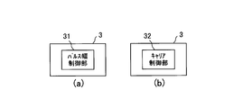


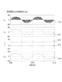
Classifications
-
- H—ELECTRICITY
- H02—GENERATION; CONVERSION OR DISTRIBUTION OF ELECTRIC POWER
- H02M—APPARATUS FOR CONVERSION BETWEEN AC AND AC, BETWEEN AC AND DC, OR BETWEEN DC AND DC, AND FOR USE WITH MAINS OR SIMILAR POWER SUPPLY SYSTEMS; CONVERSION OF DC OR AC INPUT POWER INTO SURGE OUTPUT POWER; CONTROL OR REGULATION THEREOF
- H02M7/00—Conversion of AC power input into DC power output; Conversion of DC power input into AC power output
- H02M7/42—Conversion of DC power input into AC power output without possibility of reversal
- H02M7/44—Conversion of DC power input into AC power output without possibility of reversal by static converters
- H02M7/48—Conversion of DC power input into AC power output without possibility of reversal by static converters using discharge tubes with control electrode or semiconductor devices with control electrode
- H02M7/53—Conversion of DC power input into AC power output without possibility of reversal by static converters using discharge tubes with control electrode or semiconductor devices with control electrode using devices of a triode or transistor type requiring continuous application of a control signal
- H02M7/537—Conversion of DC power input into AC power output without possibility of reversal by static converters using discharge tubes with control electrode or semiconductor devices with control electrode using devices of a triode or transistor type requiring continuous application of a control signal using semiconductor devices only, e.g. single switched pulse inverters
- H02M7/5387—Conversion of DC power input into AC power output without possibility of reversal by static converters using discharge tubes with control electrode or semiconductor devices with control electrode using devices of a triode or transistor type requiring continuous application of a control signal using semiconductor devices only, e.g. single switched pulse inverters in a bridge configuration
- H02M7/53871—Conversion of DC power input into AC power output without possibility of reversal by static converters using discharge tubes with control electrode or semiconductor devices with control electrode using devices of a triode or transistor type requiring continuous application of a control signal using semiconductor devices only, e.g. single switched pulse inverters in a bridge configuration with automatic control of output voltage or current
- H02M7/53873—Conversion of DC power input into AC power output without possibility of reversal by static converters using discharge tubes with control electrode or semiconductor devices with control electrode using devices of a triode or transistor type requiring continuous application of a control signal using semiconductor devices only, e.g. single switched pulse inverters in a bridge configuration with automatic control of output voltage or current with digital control
-
- H—ELECTRICITY
- H02—GENERATION; CONVERSION OR DISTRIBUTION OF ELECTRIC POWER
- H02M—APPARATUS FOR CONVERSION BETWEEN AC AND AC, BETWEEN AC AND DC, OR BETWEEN DC AND DC, AND FOR USE WITH MAINS OR SIMILAR POWER SUPPLY SYSTEMS; CONVERSION OF DC OR AC INPUT POWER INTO SURGE OUTPUT POWER; CONTROL OR REGULATION THEREOF
- H02M1/00—Details of apparatus for conversion
- H02M1/0003—Details of control, feedback or regulation circuits
- H02M1/0009—Devices or circuits for detecting current in a converter
Definitions
- the present invention relates to a power conversion control device and a grid interconnection device.
- FIG. 21 shows a schematic configuration diagram of a grid interconnection system according to the first conventional method.
- a single-phase inverter 902 connected to the power system has a plurality of switching elements, and converts a DC voltage of a DC power source 901 formed of a solar cell or the like into a single-phase AC voltage by pulse width modulation by these switching operations.
- Current sensor 904 and voltage detection sensor 906 detect the output current and output voltage of single-phase inverter 902, and voltage detection sensor 907 detects the output voltage of DC power supply 901.
- the inverter control circuit 903 controls the single-phase inverter 902 by generating a PWM signal for each switching element in the single-phase inverter 902 based on the detection results.
- the current sensor 904 for detecting the output current of the single-phase inverter 902 is usually provided on the output side of the single-phase inverter 902 and formed by a relatively expensive current transformer or the like as shown in FIG.
- a conventional method for detecting the output current of the single-phase inverter using a relatively inexpensive shunt resistor has also been proposed (for example, Patent Document 4 below). reference).
- Patent Document 4 two shunt resistors are required.
- a method of arranging a single shunt resistor between a DC power supply and a three-phase inverter and detecting a three-phase current using a single shunt resistor has also been proposed.
- a shunt resistor is used in principle when the voltage level of the maximum voltage phase and the voltage level of the intermediate voltage phase are approached, or when the voltage level of the intermediate voltage phase and the voltage level of the minimum voltage phase are approaching. Phase current detection becomes impossible.
- a current sensor is provided between the DC power supply and the single-phase inverter, and a DC current (IDC) between the DC power supply and the single-phase inverter is detected through a low-pass filter (see Patent Document 2 below).
- a current sensor is provided between the DC power supply and the single-phase inverter, and the output signal of the current sensor is used for overcurrent protection and load current control (see Patent Document 3 below).
- the inverter output current cannot be detected from the output signal of the current sensor near the zero cross of the inverter output voltage. If the second conventional method is used so that the inverter output current can be detected from the output signal of the current sensor in the vicinity of the zero cross of the inverter output voltage, the above-described current waveform distortion occurs.
- the present invention provides a power conversion control device and a grid interconnection device that contribute to cost reduction, and preferably a power conversion control device and a grid interconnection device that contribute to cost reduction while suppressing current waveform distortion and the like. For the purpose.
- a power conversion control device includes a specific switching element of a plurality of switching elements, a wiring that connects the specific switching element and the DC power supply without going through a DC power supply that outputs DC power.
- a first current flowing through the power supply unit or a second current flowing between the DC power source and the single-phase power conversion circuit is detected by a current sensor, and the output of the power conversion circuit is detected from the detection result of the current sensor.
- a current detection unit that detects current; and a control unit that controls the power conversion circuit based on the detected output current; and the DC power is converted into AC power using the plurality of switching elements. It is connected to a power conversion circuit.
- the current sensor includes a single current sensor, and the current detection unit detects the first current with the current sensor, and the power conversion is performed based on a detection result of the current sensor.
- the output current of the circuit may be detected.
- the current sensor can be formed with a shunt resistor, and the output current of the power conversion circuit can be detected with a single current sensor, thereby reducing the cost of the system including the power conversion control device.
- each switching element is periodically turned on and off in a carrier cycle, and the control unit is configured to detect each switching element based on the detection result of the current detection unit.
- the power conversion circuit is controlled by determining a pulse width that determines an ON period, and the pulse width of the specific switching element is set so that the pulse width of the specific switching element is secured for a predetermined time or more in each carrier cycle. Limits may be added.
- the control unit limits the pulse width by limiting the output power of the power conversion circuit or the DC voltage output from the DC power supply. It may be realized.
- each switching element is periodically turned on and off in a carrier cycle, and the control unit determines an on period of each switching element based on a detection result of the current detection unit.
- the power conversion circuit may be controlled by determining a pulse width to be determined, and the carrier period may be controlled such that the pulse width of the specific switching element is secured for a predetermined time or more in each carrier period.
- the current detection unit includes a vector signal generation unit that generates a vector signal on a rotating coordinate system based on an output signal of the current sensor representing a detection result of the current sensor, The output current may be detected or estimated based on the output signal of the current sensor and the vector signal.
- the current detection unit may estimate the output current based on the vector signal in a period in which the output current cannot be detected from the output signal of the current sensor.
- the power conversion circuit can be stably controlled even in a period in which the output current of the power conversion circuit cannot be detected from the output signal of the current sensor.
- the plurality of switching elements have first and second arm groups connected in parallel to each other, and each arm group is connected to the positive side of the DC power supply.
- the upper arm is connected in series with the lower arm connected to the negative side of the DC power source.
- the current sensor is provided on a wiring connecting the DC power source and each lower arm and between the lower arm of the first arm group and the lower arm of the second arm group.
- it is provided on the wiring connecting the DC power source and each upper arm and between the upper arm of the first arm group and the upper arm of the second arm group.
- the power conversion control device outputs an output signal of the current sensor obtained before the period in a period in which the output current cannot be detected from an output signal of the current sensor representing a detection result of the current sensor.
- a current estimation unit that estimates the output current based on the output current may be further included, and the control unit may control the power conversion circuit based on the detected or estimated output current.
- the power conversion control device further includes a vector signal generation unit that generates a vector signal on a rotating coordinate system based on an output signal of the current sensor, and the current estimation unit is arranged before the period.
- the output current may be estimated using the vector signal based on the output signal of the current sensor.
- the plurality of switching elements have first and second arm groups connected in parallel to each other, and each arm group is connected to the positive side of the DC power supply.
- the upper arm is connected in series with the lower arm connected to the negative side of the DC power source.
- the current sensor for detecting the first current is on a wiring connecting the DC power source and each lower arm, and the lower arm of the first arm group and the lower arm of the second arm group. Or between the upper arm of the first arm group and the upper arm of the second arm group, which is provided between the upper arm of the first arm group and the upper arm of the first arm group. Provided.
- a grid interconnection device includes a power conversion circuit connected to an electric power system and any one of the above-described power conversion control devices connected to the power conversion circuit.
- a power conversion control device and a grid interconnection device that contribute to cost reduction, or a power conversion control device and a grid interconnection device that contribute to cost reduction while suppressing current waveform distortion and the like. It becomes possible.
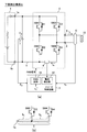
- (A) And (b) is a figure which shows the schematic block diagram of the power conversion system which concerns on 1st Embodiment of this invention, respectively, and a part of wiring in the said power conversion system.
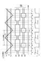
- Modification of the power conversion system according to a first embodiment of the present invention (J 2) is a diagram showing. It is a figure which shows some signal waveforms which concern on 1st Embodiment of this invention. Voltage command value (v SA * and v SB *), a carrier signal (CS), a diagram showing a PWM signal, the relationship between the target current (i dc) (where, v S *> 0).
- Voltage command value (v SA * and v SB *), a carrier signal (CS), a diagram showing a PWM signal, the relationship between the target current (i dc) (where, v S * ⁇ 0).
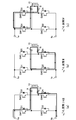
- A) ⁇ (c) is a diagram showing the current flow in each section (except, v S *> 0).
- (A) ⁇ (c) is a diagram showing the current flow in each section (except, v S * ⁇ 0).
- FIG. 10 is a diagram illustrating a relationship among voltage command values (v SA * and v SB * ), a carrier signal (CS), a PWM signal, and a target current (i dc ) corresponding to the configuration of FIG. 8 or FIG. 9. (However, v S * > 0).
- FIG. 10 is a diagram illustrating a relationship among voltage command values (v SA * and v SB * ), a carrier signal (CS), a PWM signal, and a target current (i dc ) corresponding to the configuration of FIG. 8 or FIG. 9. (However, v S * ⁇ 0). It is another figure which shows schematic structure of the power conversion system which concerns on 1st Embodiment of this invention.
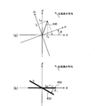
- FIG. (A) and (b) are respectively a diagram showing a relationship between ⁇ coordinate system and PQ coordinate system, and illustrates a phase difference between signals (i 1 and i 2).
- FIG. (A) and (b) are respectively a diagram showing a relationship between ⁇ coordinate system and PQ coordinate system, and illustrates a phase difference between signals (i 1 and i 2).
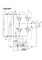
- FIG. is a schematic block diagram of the grid connection system which concerns on 3rd Embodiment of this invention.
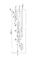
- FIG. 25 is an internal block diagram of a current detection unit in FIG. 24. It is a schematic block diagram of the grid connection system which concerns on 6th Embodiment of this invention.
- the output voltage v S of together also referred to as an output voltage v value the output voltage of the S value v S as the instantaneous value
- the output voltage arranged in time on the series A signal having the value v S as a signal value at each time is also referred to as an output voltage signal v S. That is, when referring to certain output voltage by the symbol v S, the symbol v S can also be used as a symbol that represents the output voltage value or an output voltage signal. The same applies to physical quantities or command values other than the output voltage referred to by the symbol v S.
- the names of information, physical quantities, state quantities, members, etc. corresponding to the symbols or symbols are omitted or abbreviated. That is, for example, in this specification, the output voltage v S can be expressed as “v S ” or “voltage v S ”.
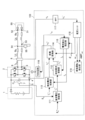
- FIG. 1A is a schematic configuration diagram of a power conversion system according to the first embodiment.
- the power conversion system according to the first embodiment includes each part referred to by reference numerals 1 to 10 and Cd.
- the DC power source 1 has a positive output terminal 1a and a negative output terminal 1b, and outputs a DC voltage between the positive output terminal 1a and the negative output terminal 1b, with the negative output terminal 1b on the low voltage side.
- the DC power supply 1 is an arbitrary DC power supply that can output a DC voltage, and is, for example, a solar battery or a storage battery.
- a solar battery or a storage battery it refers to a solar battery or a storage battery as the DC power source 1.
- FIG. 1A shows an equivalent circuit of a solar cell. The solar cell generates power based on solar energy and generates a DC voltage.
- DC voltage holding unit C d holds the DC voltage by storing charge corresponding to a DC voltage solar cell occurs.
- the DC voltage held by the DC voltage holding unit C d represented by the symbol E d.
- the voltage detection sensor 7 detects the voltage value of the DC voltage E d held by the DC voltage holding unit C d .
- a DC voltage output from the DC power supply 1 is applied to a single-phase inverter 2 that is a single-phase power conversion circuit.
- the single-phase inverter 2 has a plurality of switching elements and terminals 8 and 9 which are output terminals, and converts the DC voltage Ed into a single-phase AC voltage by pulse width modulation using the switching operation of each switching element. (In other words, DC power from the DC power source 1 is converted into single-phase AC power).
- the AC voltage obtained by the single-phase inverter 2 is output from the terminals 8 and 9 with the potential of the terminal 8 as a reference.
- the AC voltage output from the single-phase inverter 2 is supplied to the load 10 including a reactance component.
- the output of the single-phase inverter 2 can be connected to a power system.
- the output voltage of the single-phase inverter 2 (i.e., the voltage between the terminals 8 and 9 relative to the potential of the terminal 8) represents the by symbol v S.
- the voltage detection sensor 6 detects the voltage value of the output voltage v S of the single-phase inverter 2.
- the output current of the single-phase inverter 2 (that is, the current flowing from the terminal 9 to the load 10) is represented by the symbol i S.
- the single-phase inverter 2 has two half-bridge circuits connected in parallel to each other, and each half-bridge circuit has a pair of switching elements.
- the pair of switching elements are connected in series between the positive output terminal 1a and the negative output terminal 1b of the DC power supply 1, and a DC voltage from the DC power supply 1 is applied to each half bridge circuit.
- one half-bridge circuit that should be referred to as the first arm group includes a switching element SW 1 on the high voltage side (hereinafter also referred to as an upper arm SW 1 or an arm SW 1) and a low voltage side switching element SW 1.
- the other half-bridge circuit which is composed of the switching element SW2 (hereinafter also referred to as the lower arm SW2 or the arm SW2) and should also be referred to as the second arm group, is the switching element SW3 on the high voltage side (hereinafter also referred to as the upper arm SW3 or the arm SW3).
- a low-voltage side switching element SW4 hereinafter also referred to as a lower arm SW4 or an arm SW4.
- Diodes D1 to D4 are connected in parallel to the switching elements SW1 to SW4, respectively, with the direction from the low voltage side to the high voltage side of the DC power supply 1 as the forward direction.
- the diodes D1 to D4 function as freewheeling diodes.
- connection point between the upper arm SW1 and the lower arm SW2 connected in series and a connection point between the upper arm SW3 and the lower arm SW4 connected in series are connected to the terminal 9 and the terminal 8, respectively.
- IGBTs insulated gate bipolar transistors
- the power conversion system is provided with a current sensor 4 for detecting a current flowing through a predetermined target wiring.
- a current detected by the current sensor 4 is referred to as a target current and is represented by a symbol i dc .
- the current sensor 4 is interposed in series with the bus 5.
- the inverter 2 the low voltage sides of the lower arms SW2 and SW4 are connected in common and connected to the negative output terminal 1b of the DC power supply 1, and the low voltage side of the lower arms SW2 and SW4 and the negative output terminal 1b are connected in common.
- the wiring to be performed is the bus 5. As shown in FIG.
- bus 5 a wiring 5 A interposed between the low voltage side of the negative output terminal 1b and the lower arm SW2, the low voltage of the low voltage side and the lower arm SW4 of the lower arm SW2 it can be divided into, and wiring 5 B interposed between the side.
- the current sensor 4 is provided on the wiring 5 B.
- the target current i dc when the target current i dc is directed to the low voltage side of the lower arm SW2 through the current sensor 4 from the low voltage side of the lower arm SW4, and polarity of the target current i dc is positive . Since the target current i dc has a direct current component, it can also be interpreted as a direct current.
- the current sensor 4 transmits a signal representing the detected current value of the target current i dc to the inverter control circuit 3.
- a shunt resistor resistive element
- the current sensor 4 may be a current transformer or the like.
- the inverter control circuit 3 connected to the inverter 2 is based on the detection results of the current sensor 4 and the voltage detection sensors 6 and 7 (that is, based on the detection values of i dc , v S, and E d ).
- the switching operation of the arm elements SW1 to SW4 is controlled.
- the DC voltage from the DC voltage 1 is PWM-modulated (pulse width modulation) and converted into an AC voltage.
- the inverter control circuit can also be called a control device, an inverter control device, a power conversion circuit control device, or a power conversion control device.
- the current sensor 4 can also be considered to be included in the components of the inverter control circuit 3 (the same applies to inverter control circuits 103, 203, 103A, and 203A described later).
- the control circuit 3 can generate a voltage command value v S * that is a target value of the output voltage v S based on the detected values of i dc , v S, and E d .
- the PWM circuit 11 provided in the control circuit 3 generates PWM signals for the arms SW1 to SW4 so that the voltage value v S matches the command value v S * .
- the arrangement position of the current sensor 4 is not limited to that shown in FIG.
- the wiring 5 instead of B, as shown in FIG. 2, the high voltage side of the high voltage side and the upper arm SW3 positive output terminal 1a and the upper arm SW1 and SW3 and top and even on the common connection wiring arm SW1
- the current sensor 4 may be provided on the wiring interposed between the two.
- upper detection arrangement J 2 A structure as shown in FIG. 2, for convenience, referred to as upper detection arrangement J 2.
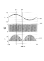
- FIG. 3 shows a waveform 601 of the output current i S , a waveform 602 of the PWM signal, and a waveform 603 of the target current i dc .
- the waveform 603 is a waveform of the target current i dc when the lower detection configuration J 1 is employed.
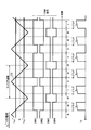
- the section 604 is a part of a section where i S > 0, and the section 605 is a part of a section where i S ⁇ 0. 4 and 5, voltage command values v SA * and v SB * based on the command value v S * , a carrier signal CS whose value periodically changes in a triangular wave shape, a PWM signal, and a target current i
- FIG. 3 shows a waveform 601 of the output current i S , a waveform 602 of the PWM signal, and a waveform 603 of the target current i dc .
- the waveform 603 is a waveform of the target current i dc when
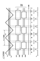
- FIGS. 4 and 5 show the relationship in the section where v S * > 0 corresponding to the section 604, and FIG. 5 shows the relationship in the section corresponding to the section 605 where v S * ⁇ 0. Show.
- the waveform of the target current i dc shown in FIGS. 4 and 5 is the waveform of the target current i dc when the lower detection configuration J 1 is employed.
- the carrier signal CS can be generated by the PWM circuit 11.
- the PWM circuit 11 generates command values v SA * and v SB * from the command value v S * .
- Time t i + 1 is a time later than time t i (i is an integer).
- the period of the carrier signal CS is called a carrier period. In FIG. 4, the period from time t 0 when the value of the carrier signal CS (hereinafter referred to as carrier signal value CS VAL ) takes a minimum value to time t 6 when the carrier signal value CS VAL takes a minimum value is shown.
- the start time of the carrier cycle can be any time.
- the time t 3 at which the carrier signal value CS VAL takes the maximum value may be considered as the start time of one carrier cycle.
- the average value of the maximum value and the minimum value in the carrier signal CS is zero (that is, the DC component of the carrier signal CS is zero).
- the PWM circuit 11 compares the command values v SA * and v SB * with the carrier signal value CS VAL and generates a PWM signal for the arm elements SW1 to SW4 based on the comparison result.
- each of the arms SW1 to SW4 is periodically turned on and off with the carrier period as a repetition period.
- v SA * ⁇ CS VAL When “v SA * ⁇ CS VAL ” is established, the upper arm SW1 is turned off, and When “v SA * ⁇ CS VAL ” is not established, the upper arm SW1 is turned on, and When “v SB * ⁇ CS VAL ” is established, the upper arm SW3 is turned off, and When “v SB * ⁇ CS VAL ” is not established, the upper arm SW3 is turned on.
- the lower arm SW2 is on when the upper arm SW1 is off, the lower arm SW2 is off when the upper arm SW1 is on, and the lower arm when the upper arm SW3 is off.
- SW4 is on, and when the upper arm SW3 is on, the lower arm SW4 is off.
- section II The section in which the upper arm SW1 is turned off and the upper arm SW3 is turned off is called section II.
- a section in which the upper arm SW1 is on and the upper arm SW3 is on is referred to as section IV.
- section I a section in which the upper arm SW1 is turned on and the upper arm SW3 is turned off while the carrier signal value CSVAL is increasing
- section III A section in which the arm SW1 is turned on and the upper arm SW3 is turned off is referred to as a section III.
- a section in which the upper arm SW1 is turned off and the upper arm SW3 is turned on while the carrier signal value CSVAL is increasing corresponds to the section I, and the carrier signal value CSVAL is decreasing.
- a section in which the upper arm SW1 is turned off and the upper arm SW3 is turned on corresponds to the section III.
- the period between time t 0 and t 1 and the period between time t 5 and t 6 belong to section IV
- the period between time t 1 and t 2 belongs to section I
- the period between time t 2 and t 4 belongs to section II.
- the period between time t 4 and t 5 belongs to section III.
- the increase or decrease in the current value i dc in the sections I, II and III in FIG. 4 and the increase in the current value i dc in the section II in FIG. 5 are derived from the fact that the reactance component is included in the load 10. To do.
- the current detector 12 provided in the control circuit 3 can detect the target current value i dc as the output current value i S by sampling the output signal of the current sensor 4 at an appropriate timing. If lower detection arrangement J 1 is employed, since the target current value i dc in section II coincides with the output current value i S, by sampling the output signal of the current sensor 4 in the section II, the target current value i It is possible to detect dc as the output current value i S.
- a current sensor 4 may be provided on the wiring connecting the negative output terminal 1b of the DC power source 1 and the negative input terminal 13 of the single-phase inverter 2 (that is, between the negative output terminal 1b and the negative input terminal 13).
- a current sensor 4 may be provided on the wiring connecting the negative output terminal 1b of the DC power source 1 and the negative input terminal 13 of the single-phase inverter 2 (that is, between the negative output terminal 1b and the negative input terminal 13).
- a current sensor 4 may be provided on the wiring connecting the positive output terminal 1a of the DC power source 1 and the positive input terminal 14 of the single-phase inverter 2 (that is, between the positive output terminal 1a and the positive input terminal 14).
- a current sensor 4 may be provided on the wiring connecting the positive output terminal 1a of the DC power source 1 and the positive input terminal 14 of the single-phase inverter 2 (that is, between the positive output terminal 1a and the positive input terminal 14).
- the single-phase inverter 2 has input terminals 13 and 14, and the DC voltage Ed is applied between the input terminals 13 and 14 with the potential of the negative input terminal 13 as a reference.
- the negative input terminal 13 is commonly connected to the low voltage side of the lower arms SW2 and SW4, and the positive input terminal 14 is commonly connected to the high voltage side of the upper arms SW1 and SW3.
- the upper detection arrangement K 2 in FIG. 9 the subject current flowing from the terminal 1a to the terminal 14 The polarity of i dc is positive.
- the target current i dc in the lower detection configuration K 1 and the upper detection configuration K 2 is always positive or zero.
- the target current i dc when the battery is charged is negative or zero, the target current i dc when the battery is discharged becomes Seimatawa 0.
- FIG. 10 shows a waveform 611 of the output current i S , a waveform 612 of the PWM signal, and a waveform 613 of the target current i dc .
- the waveform 613 is a waveform of the target current i dc when the detection configuration K 1 or K 2 is adopted.
- the section 614 is a part of a section where i S > 0 and i S is sufficiently large, and the section 615 is a part of a section where i S ⁇ 0 (where i S > 0).
- FIG. 11 shows their relationship in a section corresponding to the section 614 where v S * > 0 and v S * is sufficiently large
- FIG. 12 corresponds to the section 615, v S * ⁇ The relationship is shown in a section where 0 (however, v S * > 0).
- Waveform of the target current i dc shown in FIG. 11 and FIG. 12 is a waveform of the target current i dc at the time of the adoption detection arrangement K 1 or K 2.
- the target current value i dc in each of the sections I and III are consistent with the output current value i S, sampling the output signal of the current sensor 4 in the section I or III Thus, the target current value i dc can be detected as the output current value i S.
- the control circuit 3 determines the ON period of the arms SW 1 to SW 4 based on the detection result of the output current i S by the current detection unit 12.
- the inverter 2 can be controlled by determining a predetermined pulse width.
- the on period of the arm SW4 refers to a period in which the arm SW4 is on, and the off period of the arm SW4 refers to a period in which the arm SW4 is off (the same applies to other arms).
- the pulse width that determines the ON period of the arm SW4 corresponds to the length of the ON period of the arm SW4 in each carrier cycle (the same applies to the other arms).
- the pulse width that determines the ON period of the arm SW4 is referred to as a pulse width ON SW4 .
- the pulse widths that determine the ON periods of the arms SW1 to SW3 are denoted as pulse widths ON SW1 to ON SW3 , respectively.
- the timing at which the output signal of the current sensor 4 should be sampled in order to detect the output current i S is called the target timing. Therefore, the current detection unit 12 detects the target current value i dc as the output current value i S by sampling the output signal of the current sensor 4 at the target timing in each carrier cycle.
- FIG lower detection arrangement J 1 of the (a) is adopted to the electric power conversion system according to the first embodiment.
- the current sensor 4 in the lower detection configuration J 1 is also referred to as a current sensor 4 [J 1 ].
- the target current value i dc matches the output current i S (FIG. 6 (b), etc. See) in the interval II, a current detector 12 In section II, the target current value i dc can be detected as the output current value i S by sampling the output signal of the current sensor 4 [J 1 ]. Therefore Specifically, for example, the target timing when the adopted lower detection arrangement J 1, a timing when the carrier signal value CS VAL takes a maximum value.
- the current sensor 4 in the upper detection configuration J 2 is also referred to as a current sensor 4 [J 2 ].
- the target current value i dc matches the output current i S in section IV
- the current detection unit 12 a current sensor in the section IV
- the target current value i dc can be detected as the output current value i S.
- the target timing when the adopted upper detection arrangement J 2 the carrier signal value CS VAL is a timing to take a minimum value.
- the current value i dc matches the output current value i S in each of the sections I and III (see FIG. 6A and the like), so that the current detection unit 12 is
- the target current value i dc can be detected as the output current value i S by sampling the output signal of the current sensor 4 [K] in any one of the sections I and III or in each of the sections I and III. Therefore, specifically, for example, the target timing when the detection configuration K 1 or K 2 is adopted is a timing at which the carrier signal value CS VAL becomes zero (so-called zero cross timing).
- the detection configuration J 1 or J 2 When the detection configuration J 1 or J 2 is employed, no problem occurs in the detection of the output current i S even when the output voltage value v S is small (even near the zero cross), but the detection configuration K 1 or K 2 is employed. In some cases, the time constraint becomes severe when the output voltage value V S is small. That is, when the length of each of the sections I and III becomes shorter than the predetermined reference time L TH, the output current i S cannot be detected from the output signal of the current sensor 4 [K].
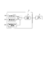
- the control circuit 3 includes a current estimation unit 21 that performs a current estimation process, and a current detection availability determination process that performs a current detection availability determination process.
- Part (determination processing part) 22 can be provided.
- the current detection possibility determination process is a process for determining whether the current time belongs to a detectable period or a non-detectable period.
- the timing at which this determination is made is referred to as the timing of interest.
- the detectable period is a period in which the output current i S can be detected from the output signal of the current sensor 4
- the undetectable period is a period in which the output current i S cannot be detected from the output signal of the current sensor 4.
- the determination unit 22 is based on the voltage command value v S * at the timing of interest (or the value that is the source of the voltage command value v S * at the timing of interest) and the time length of one carrier cycle A determination target width corresponding to the attention timing is obtained.
- Determination target width when the current sensor 4 is a current sensor 4 [J 1] is the pulse width ON SW4, a pulse width ON SW3 when the current sensor 4 is a current sensor 4 [J 2] Yes, when the current sensor 4 is the current sensor 4 [K], it is the width of the section I or III.
- the determination target width corresponding to the attention timing refers to the determination target width within one carrier cycle starting from the attention timing.
- the determination unit 22 determines that the attention timing belongs to the detectable period if the determination target width is equal to or greater than the reference time LTH , and cannot detect the attention timing if the determination target width is less than the reference time LTH. Judge as belonging to the period.
- the control circuit 3 controls the single-phase inverter 2 via the PWM circuit 11 based on the output current i S detected by the current detection unit 12.
- the control circuit 3 controls the single-phase inverter 2 via the PWM circuit 11 based on the output current i S estimated by the current estimation unit 21.
- the current estimation unit 21 estimates the output current i S at the target timing based on the output signal of the current sensor 4 obtained before the non-detectable period to which the target timing belongs. To do. Specific examples of the estimation method will be described later in other embodiments.
- the current sensor can be formed with a relatively inexpensive shunt resistor, and the output current of the single-phase inverter can be detected with a single current sensor.
- the cost of the entire system can be reduced.
- the output current used for the control is obtained by estimation, so that stable control can be maintained even during the non-detectable period and voltage correction (pulse width correction) corresponding to the second conventional method is performed.
- voltage correction pulse width correction
- distortion of the output current waveform is suppressed. Therefore, when the technology of this embodiment is used for grid interconnection, it becomes easy to satisfy the criteria of the guidelines regarding grid interconnection (the specific configuration using the technology of this embodiment for grid interconnection is different from that of other embodiments). Will be described later).
- the existence of dead time is ignored for the sake of simplification, but in consideration of the existence of dead time, the estimation is performed near the zero crossing of the current.
- the detection configurations J 1 and J 2 that use the detection current value near the zero crossing of the current are considered to be more advantageous for dead time correction than the detection configurations K 1 and K 2 that use the current value.
- the dead time correction is a voltage correction (pulse width correction) performed to avoid the upper and lower arms connected in series from being turned on at the same time, and uses the polarity of the output current i S near the zero cross. It is done.
- FIG. 14 is a schematic configuration diagram of a grid interconnection system according to the second embodiment, which is a specific example of the power conversion system according to the first embodiment.
- the grid interconnection system according to the second embodiment may be employed detection arrangement J 1, J 2 or K 2 (FIGS. 1 (a) FIG. 2 or FIG. 9).
- the current detection / estimation unit 115 in FIG. 14 realizes a function equivalent to the function realized by the current detection unit 12, the current estimation unit 21, and the current detection availability determination unit 22 in the first embodiment (see FIG. 13).
- the current detection / estimation unit 115 may be considered to include the detection unit 12, the estimation unit 21, and the determination unit 22.
- An inverter control circuit (control device) 103 in FIG. 14 is a specific example of the inverter control circuit 3 according to the first embodiment, and can realize an arbitrary function realized by the control circuit 3. Arbitrary portions in the control circuit 103 can freely use arbitrary information (signals, command values, detected values, estimated values, etc.) obtained by the control circuit 103.
- System interconnection system has a DC power source 1, single-phase inverter 2, a current sensor 4, the voltage detection sensor 6, the voltage sensor 7 and the DC voltage holding unit C d described in the first embodiment
- the inverter control circuit 103 that controls the single-phase inverter 2 is connected to the load 55 and the power system 50 that outputs single-phase AC power.
- the control circuit 103 is provided with each part referred to by reference numerals 111 to 119.
- the grid interconnection system in FIG. 14 includes a grid interconnection apparatus.
- the grid interconnection device includes a control circuit 103, and may further include at least one of a DC power source 1, a single-phase inverter 2, a current sensor 4, a voltage detection sensor 6, and a voltage detection sensor 7.
- it is also possible to grasp that any part shown in FIG. 14 is included in the components of the grid interconnection device.
- Voltage detecting sensor 7 detects the voltage value of the DC voltage E d, which is held by the DC voltage holding unit C d, and sends a signal E d with the detected voltage value as the signal value to the DC voltage control unit 111.
- a DC voltage from the DC voltage holding unit C d is converted into an AC voltage of the single-phase outputs from the terminals 8 and 9 and the resulting AC voltage potential of the terminal 8 as a reference.
- the power system 50 has an AC voltage source, and outputs a single-phase AC voltage (for example, so-called commercial AC voltage) from the terminals 51 and 52 with the potential of the terminal 51 as a reference.
- An interconnection point 53 is provided on the wiring connecting the terminals 8 and 51, and an interconnection point 54 is provided on the wiring connecting the terminals 9 and 52, and an AC voltage between the interconnection points 53 and 54 is provided. Is connected between the connection points 53 and 54.
- the load 55 is driven using the output AC power of the single-phase inverter 2 and the output AC power of the power system 50 (FIGS. 20, 24, and 24 described later). The same applies to 26 grid interconnection systems).
- the reactance component of the indoor wiring between the terminal 8 and the connection point 53 and the reactance component of the indoor wiring between the terminal 9 and the connection point 54 are represented by Lc, and the resistance component of each indoor wiring is represented by Rc.
- the reactance component of the outdoor wiring connecting the terminal 51 and the connection point 53 and the reactance component of the outdoor wiring connecting the terminal 52 and the connection point 54 are represented by Ls, and the resistance component of each of the outdoor wirings is represented by Rs. Represent.
- the current sensor 4 transmits a signal representing the detected current value of the target current i dc , that is, the target current signal i dc to the current detection / estimation unit 115.
- the voltage detection sensor 6 sends a signal representing the voltage value of the output voltage v S detected by itself, that is, the output voltage signal v S to the band pass filter (BPF) 117.
- BPF band pass filter
- ⁇ n is a nominal frequency determined on the power system 50 side, and is, for example, 60 ⁇ 2 ⁇ or 50 ⁇ 2 ⁇ .
- ⁇ represents a circular ratio, and unless otherwise specified, the phase or angle is a phase or angle in electrical angle, and the unit of phase or angle expressed using ⁇ is radians.
- the output voltage signal v S of the inverter 2 is expressed by the following equation (A-1).
- ⁇ and AMP represent the phase and amplitude of the output voltage signal v S , respectively.
- Frequency of the output voltage signal v S has a value close to matching or nominal frequency omega n the nominal frequency omega n.
- v S AMP ⁇ cos ( ⁇ ) (A-1)
- BPF117 attenuates the harmonic components included in the signal v S (omega n higher-order components), and outputs the signal v S which has been made of this attenuation as the signal v S '.
- the presence of harmonic components does not matter, it is possible to omit BPF 117, and when omitting BPF 117, signal v S and signal v S ′ match.
- the estimation unit 118 estimates the phase, frequency, and amplitude of the output voltage signal v S based on the signal v S ′ that is a single-phase signal, and estimates the phase, frequency, and amplitude of the output voltage signal v S , respectively.
- Output as ⁇ est , ⁇ est and AMP est There are various known methods for estimating all or part of the phase, frequency, and amplitude of a single-phase signal, and the estimation unit 118 uses a known method (for example, Japanese Patent Application Laid-Open No. 2003-143860 or Japanese Patent Application Laid-Open No. 2006-129681).
- Estimated values ⁇ est , ⁇ est, and AMP est can be obtained using the method described in Japanese Patent Publication No. H. For example, ⁇ est and ⁇ est may be obtained from the zero cross timing of the signal v S ′.
- the current detection / estimation unit 115 detects the target current value i dc at the target timing as the output current value i S by sampling the output signal of the current sensor 4 at the target timing in each carrier cycle. However, the output current value i S is obtained by estimation during the non-detectable period. Because the system interconnection system of Figure 14 is employed is the lower detection arrangement K 1, subject timing is a timing when the carrier signal value CS VAL is zero. In case of adopting the detection arrangement K 2 to the grid interconnection system also subject timing is a timing when the carrier signal value CS VAL is zero.
- subject timing is a timing when the carrier signal value CS VAL takes a maximum value
- the target timing is the timing at which the carrier signal value CS VAL takes a minimum value. If the detection arrangement to the grid interconnection system K 1 or K 2 is adopted, the current detecting / estimating portion 115, setting the target timing to each of the either one or sections I and III of the sections I and III Can do.
- the output current of the single-phase inverter 2 is formed from an effective current and a reactive current.
- Current detecting / estimating portion 115 also functions as a coordinate converter, based on the phase theta est from estimation unit 118, the active current and reactive current to form the output current i S from the output current i S detected or estimated is calculated, to generate a reactive current signal i q having a current value of the active current signal i p and reactive current having a current value of the active current as the signal value as the signal value.
- the DC voltage control unit 111 is given a DC voltage command value E d * in addition to the signal E d .
- DC voltage command value E d * is (in other words, the signal E d to maximize the output power of the single-phase inverter 2) signal E d to obtain the maximum power from the solar cell as a DC power source 1 value of Matches.
- the DC voltage control unit 111 calculates and outputs an effective current command value i p * such that the value of the signal E d matches the command value E d * by proportional integral control or the like.
- the reactive current command value i q * is set to zero.
- Active current controller 112 and the reactive current controller 113 respectively, so that the value of the value and the reactive current signal i q of the active current signal i p and the like proportional integral control is coincident with the command value i p * and i q *
- the voltage specified values v p * and v q * are calculated, and the coordinate conversion unit 114 converts the specified values v p * and v q * into voltages based on the phase ⁇ est from the estimation unit 118 according to the following equation (A-2). Convert to command value v S * .
- the PWM circuit 116 controls each switching element in the single-phase inverter 2 so that the output voltage value v S of the single-phase inverter 2 matches the voltage command value v S * according to the method described in the first embodiment.
- the control circuit 103 realizes control of the output current i S through control of each switching element according to the voltage command value v S * .
- the single operation detection unit 119 detects the single operation state of the single-phase inverter 2 based on the frequency ⁇ est or the amplitude AMP est estimated by the estimation unit 118 (that is, detects whether single operation has occurred). ).
- a known method can be used as this detection method.
- Independent operation refers to a state in which only the single-phase inverter 2 supplies power to the load 55.
- the isolated operation can occur when a power failure occurs on the power system 50 side. For the purpose of ensuring safety or the like, when an isolated operation occurs, it is required to quickly detect this and stop the output of the single-phase inverter 2. Therefore, when the single operation state is detected by the detection unit 119, the control circuit 103 promptly stops the output of the inverter 2.
- FIG. 15 is an example of an internal block diagram of the current detection / estimation unit 115.
- the current detection / estimation unit 115 in FIG. 15 includes each part referred to by reference numerals 131 to 134.
- the A / D conversion unit 131 functions as the current detection unit 12 of FIG. 13 and samples the output signal of the current sensor 4 at the target timing in each carrier cycle.
- the value of the output signal of the sampled current sensor 4, that is, the sampled target current value i dc is represented by the symbol i dcS .
- the switch unit 132 receives the detected current value i dcS from the A / D conversion unit 131 and the estimated current value i Test from the estimation calculation unit 134.
- the current value i Test is an estimated value of the output current i S.
- the switch unit 132 as the switching processing unit includes the determination unit 22 of FIG. 13, and by executing the current detection availability determination processing described in the first embodiment, the current time (attention timing) can be detected as a detectable period and an undetectable period. It is determined to which period it belongs, and one of the detected current value i dcS and the estimated current value i Set is selected and output based on the determination result.
- the switch unit 132 determines that the current timing of attention belongs to the detectable period, the switch unit 132 outputs the detected current value i dcS (or its inverted value ( ⁇ i dcS )) as the current value i SD , When it is determined that the target timing belongs to the non-detectable period, the estimated current value i Test is output as the current value i SD . Therefore, the current value i SD output from the switch unit 132 is the output current value i S detected or estimated by the current detection / estimation unit 115.
- the switch unit 132 receives the signal v S detected from the voltage detection sensor 6 from the BPF 117.
- the polarity of the output voltage v S is determined based on the signal v S ′, the specified value v S * from the coordinate conversion unit 114, or the estimated phase ⁇ est from the estimation unit 118, and based on the determination result of the polarity of the output voltage v S
- the current value i dcS and ( ⁇ i dcS ) are selectively substituted for the current value i SD .
- the current value i SD is output to the outside of the current detection / estimation unit 115, but this output is unnecessary in the configuration of FIG. 14.
- a signal i SD having the current value i SD output from the switch unit 132 as a signal value is input to the coordinate conversion unit 133 as a single-phase signal.
- the coordinate conversion unit 133 generates signals i p and i q from the signal i SD and the estimated value ⁇ est .
- Signal i p and i q that are generated by the coordinate conversion unit 133 functions as an effective current signal i p and reactive current signal i q output from the current detecting / estimating portion 115.
- the signals i p and i q generated by the coordinate conversion unit 133 are input to the estimation calculation unit 134.
- the estimation calculation unit 134 functions as the current estimation unit 21 in FIG. 13 and obtains an estimated current value i Test according to the following equation (A-3).
- the estimation calculation unit 134 can use ⁇ est as ⁇ in the equation (A-3), and can use ⁇ n or ⁇ est as ⁇ in the equation (A-3).
- T S represents the sampling period in the A / D converter unit 131. If A / D converter 131 is sampled once in each carrier period, the sampling period T S is consistent with the carrier cycle, the A / D conversion unit 131 is sampled twice in each carrier period, the sampling period T S is Matches half the carrier period.
- the time at which the i-th sampling is performed in the A / D converter 131 is referred to as the i-th time, and the current values i dcS , i SD, and i Test at the i-th time are represented by the symbols i dcS [i] and i SD [ i] and i Set [i] (i is an integer).
- the i-th time is the time when the sampling period T S has elapsed from the (i ⁇ 1) -th time.
- the i-th time may belong to a detectable period or a non-detectable period.
- the estimation calculation unit 134 uses the signals i p and i q reflecting the output value i SD [i ⁇ 1] and the output value i SD of the switch unit 132 before the (i ⁇ 1) time to estimate the current value i. Find Set [i]. Accordingly, the output value i SD [i ⁇ 1] and the output value i SD of the switch unit 132 before the (i ⁇ 1) time are equal to the i dcS [i ⁇ 1] and the (i ⁇ 1) time before the output value i SD [i ⁇ 1].
- the estimation calculation unit 134 uses the detected current value i dcS that is earlier than the i-th time. , The estimated value of the output current i S at the i-th time (that is, i Set [i]) is obtained. In other words, the estimation calculation unit 134 uses the vector signal on the PQ coordinate system based on the detected current value i dcS that is earlier than the i-th time to estimate the output current i S at the i-th time (that is, i Test). [I]).
- the vector signal on the PQ coordinate system used by the estimation calculation unit 134 is a vector signal having i p and i q as two orthogonal components, and the coordinate conversion unit 133 It functions as a vector signal generation unit that generates a signal from the output signal of the current sensor 4.
- the current detection / estimation unit 115 detects the output current i S from the output signal of the current sensor 4 as i SD in the detectable period, but in the non-detectable period, the detection period before the non-detectable period
- An output current i S is estimated using a vector signal based on the detected current value i dcS , and the estimation result is output as i SD .
- the signal i SD having the current value i SD as a signal value is input as a single phase signal to the coordinate conversion unit 133 including the filter 141 and the vector component calculation unit 142.
- i SD i 1 is set.
- FIG. 16A shows the relationship between the ⁇ coordinate system and the PQ coordinate system.
- the ⁇ coordinate system is a two-dimensional fixed coordinate system having ⁇ and ⁇ axes as fixed axes as coordinate axes.
- the ⁇ and ⁇ axes are orthogonal to each other, and the ⁇ axis is advanced from the ⁇ axis by 90 degrees in electrical angle.
- the counterclockwise direction corresponds to the phase advance direction.
- the PQ coordinate system is a two-dimensional rotational coordinate system having the rotation axes P and Q as coordinate axes.
- the P and Q axes are orthogonal to each other, and the Q axis is advanced from the P axis by an electrical angle of 90 degrees.
- the phase ⁇ coincides with the phase of the P axis viewed from the ⁇ axis.
- ⁇ represents the advance angle of the phase of the P axis with respect to the ⁇ axis.
- reference numeral 630 represents a vector on an arbitrary coordinate system.
- Vector 630 represents the phase and amplitude state of any signal. Therefore, a signal whose phase and amplitude state are represented by the vector 630 can also be called a vector signal.
- the vector 630 is a vector that rotates in synchronization with the rotation of the PQ coordinate system. Then, since the vector 630 rotates on the ⁇ coordinate system, the vector 630 on the ⁇ coordinate system can also be called a rotation vector.
- the vector 630 is considered to be a current vector, and the ⁇ axis, ⁇ axis, P axis, and Q axis components of the vector 630 are represented by i ⁇ , i ⁇ , i p, and i q, respectively. That is, considered to be a signal i p and i q of P axis and Q-axis components of the vector 630 is determined by the current detecting / estimating portion 115.
- signals i p and i q , i ⁇ and i ⁇ are also a type of signal.
- i ⁇ is a signal having only an ⁇ -axis component.
- i ⁇ and i ⁇ are orthogonal two components (two components orthogonal to each other) of the rotation vector 630 on the ⁇ coordinate system, and i p and i q are orthogonal two components of the vector 630 on the PQ coordinate system. .
- the known frequency given as the frequency of the single-phase signal i 1 is the nominal frequency ⁇ n described above.
- ⁇ n corresponds to the angular frequency of the fundamental component of the signal i 1 ignoring the harmonic component.
- the angular frequency in the rotation of the PQ coordinate system can be set to ⁇ n . Therefore, it can be said that the PQ coordinate system is a rotating coordinate system that rotates in synchronization with the frequency ⁇ n of the single-phase signal i 1 .
- the phase difference between the signals i 1 and i 2 is represented by ⁇ 1 .
- ⁇ 1 positive, the signal i 2 is delayed in phase by ⁇ 1 relative to the signal i 1 .
- solid lines 632 and 633 represent the trajectories of the signals i 1 and i 2 on the ⁇ coordinate system, respectively.
- the signals i 1 and i 2 can be converted into orthogonal two components i ⁇ and i ⁇ of the rotation vector 630 on the ⁇ coordinate system. . That is, Expression (B-1a) is established using the matrix C 1 ( ⁇ 1 ) of Expression (B-1).
- R AMP AMP i1 / AMP i2 , It is. That is, R AMP is the amplitude ratio between the signals i 1 and i 2 .
- ⁇ 2 ⁇ / 2 ⁇ 1 It is.
- the signal i ⁇ as the ⁇ / 2 phase difference signal can be expressed by the equation (B-1b) or (B-1c). . Since the matrix C 1 ( ⁇ 1 ) can also be said to depend on ⁇ 2 , “C 1 ( ⁇ 1 )” can also be expressed as “C 1 ( ⁇ 2 )”.
- the matrix C 1 ( ⁇ 1 ) is represented by, for example, an expression (B-2) when ⁇ 1 is ⁇ / 4, and is represented by an expression (B-2a) when ⁇ 1 is ⁇ / 3.
- the vector 630 on the PQ coordinate system can be obtained by rotating the rotation vector 630 on the ⁇ coordinate system by the angle ⁇ .
- a matrix C 2 ( ⁇ ) for rotating the rotation vector 630 on the ⁇ coordinate system by the angle ⁇ is expressed by the following equation (B-3), and is a product of the matrices C 1 ( ⁇ 1 ) and C 2 ( ⁇ ).
- a certain matrix C ( ⁇ ) is represented by the following formula (B-4).
- the filter 141 in FIG. 15 generates a filter signal i 2 by applying a filtering process that delays or advances the phase of the filtering target signal to the signal i 1 as the filtering target signal.
- the transfer function of the filter 141 is represented by F (s).
- the gain of the signal i 1 at the frequency ⁇ n is 1 / R AMP . Therefore, by passing the filter 141, the amplitude of the signal component of the frequency ⁇ n in the signal i 1 becomes 1 / R AMP .
- the vector component calculation unit 142 calculates the signals i p and i q from the signals i 1 and i 2 by performing coordinate transformation according to the above equations (B-4) and (B-4a) using ⁇ 1 and ⁇ . To do.
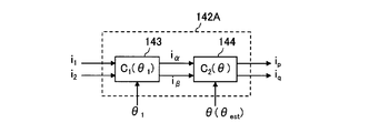
- As the vector component calculation unit 142 it is also possible to use the vector component calculation unit 142A of FIG.
- the vector component calculation unit 142A is provided with coordinate conversion units 143 and 144.
- the coordinate conversion unit 143 calculates the signals i ⁇ and i ⁇ from the signals i 1 and i 2 according to the above formulas (B-1) and (B-1a) based on ⁇ 1 .
- the coordinate conversion unit 144 calculates signals i p and i q by multiplying a matrix having elements of the signals i ⁇ and i ⁇ calculated by the coordinate conversion unit 143 by a matrix C 2 ( ⁇ ). That is, by rotating the rotation vector 630 on the ⁇ coordinate system having the signals i ⁇ and i ⁇ as two orthogonal components by ⁇ using the matrix C 2 ( ⁇ ), the signals i p and i q are converted into two orthogonal signals.
- a vector 630 on the PQ coordinate system is calculated as a component.
- ⁇ est is used as ⁇ in the calculation unit 142 and the coordinate conversion unit 144.
- Signal i p and i q obtained by the calculating unit 142 is output from the current detecting / estimating portion 115 as an effective current signal i p and reactive current signal i q.
- the coordinate conversion unit 133 functions as a vector signal generation unit that generates a vector signal (a signal representing the vector 630) having i p and i q as two orthogonal components based on the output signal of the current sensor 4. .
- phase difference ⁇ 1 between the signals i 1 and i 2 is ⁇ / 4 or ⁇ / 3
- specific calculation operations of the filter 141 and the vector component calculation unit 142 will be described.
- the value of ⁇ 1 may be other than ⁇ / 4 and ⁇ / 3.
- the current detection / estimation unit 115 can obtain various signals using each formula described below, and at this time, ⁇ est can be used as ⁇ in each formula described below.
- the signals i 1 and i 2 are converted into orthogonal two components i ⁇ and i ⁇ of the rotation vector 630 on the ⁇ coordinate system by the following equation (B-6) based on the equations (B-1a) and (B-2). can do.
- “ ⁇ 2” is a positive square root of 2.
- Equation (B-8) i is calculated using equation (B-8) below. It is also possible to determine i p and i q directly from 1 and i 2 .
- phase difference ⁇ 1 is ⁇ / 4 as in this example
- i p and i q can be directly obtained from i 1 and i 2 using the following equation (B-9).
- a single-phase vector signal (a vector signal having two orthogonal components i p and i q ) on the rotating coordinate system can be obtained by a relatively simple calculation using a primary filter.
- filter signal i 2 obtained according to the the phase by [pi / 4 with respect to the signal i 1 is delayed, filter a signal is advanced the phase by [pi / 4 with respect to the signal i 1 may be generated as a signal i 2, in this case, may be generated filtered signal i 2 in accordance with the following formula (B-5a).
- the filter signal i 2 in the equation (B-5a) is a phase advance signal whose phase is advanced by ⁇ / 4 from the signal i 1.
- “ ⁇ 1 ⁇ / 4 ′′.
- the filter 141 may be generating an inverted signal of the signal represented by the right-hand side of the formula (B-5) as a filtered signal i 2.
- An inversion signal of an arbitrary signal of interest refers to a signal obtained by inverting the sign of the signal of interest. That is, for example, the inverted signal of the signal i 1 is ( ⁇ i 1 ). Therefore, the inverted signal of the signal represented by the right side of the equation (B-5) is represented by “ ⁇ (2 ⁇ n i 1 / (s + ⁇ n ))”. Inverted signal of the signal represented by the right-hand side of the formula (B-5) is 3 [pi] / 4 by signal advanced in phase with respect to the signal i 1.
- the phase of the signal can be advanced by ⁇ / 2 or more by the primary filter 141.
- the filter 141, the inverted signal of the signal represented by the right-hand side of the formula (B-5a) (-. (2si 1 / (s + ⁇ n)) may also be generated as a filter signal i 2
- the inverted signal of the signal represented by the right side of (B-5a) is a signal delayed in phase by 3 ⁇ / 4 with respect to the signal i 1.
- the phase of the signal is changed by the primary filter 141. It can also be delayed by ⁇ / 2 or more.
- the signals i 1 and i 2 are converted into orthogonal two components i ⁇ and i ⁇ of the rotation vector 630 on the ⁇ coordinate system by the following equation (B-11) based on the above equations (B-1a) and (B-2a). can do.
- Equation (B-13) It is also possible to determine i p and i q directly from 1 and i 2 .
- a single-phase vector signal (a vector signal having two orthogonal components i p and i q ) on the rotating coordinate system can be obtained by a relatively simple calculation using a primary filter.
- filter signal i 2 obtained according to is only [pi / 3 with respect to the signal i 1 phase is delayed, filter a signal is advanced the phase by [pi / 3 with respect to the signal i 1 may be generated as a signal i 2, in this case, may be generated filtered signal i 2 in accordance with the following formula (B-10a).
- the filter signal i 2 in the equation (B-10a) is a phase advance signal whose phase is advanced by ⁇ / 3 from the signal i 1.
- “ ⁇ 1 ⁇ / 3 ′′.
- the filter 141 may be generating an inverted signal of the signal represented by the right-hand side of Equation (B-10) as a filtered signal i 2.
- Inverted signal of the signal represented by the right-hand side of Equation (B-10) is a 2 [pi / 3 only signal advanced in phase with respect to the signal i 1.
- the phase of the signal can be advanced by ⁇ / 2 or more by the primary filter 141.
- the filter 141 may be generating an inverted signal of the signal represented by the right-hand side of the formula (B-10a) as a filtered signal i 2.
- Inverted signal of the signal represented by the right-hand side of the formula (B-10a) is a signal whose phase is delayed by 2 [pi / 3 with respect to the signal i 1.
- the primary filter 141 can delay the phase of the signal by ⁇ / 2 or more.
- Waveforms 681 to 685 in FIG. 18 represent the waveforms of the signals i dc , i dcS , i p , i q, and i Set when the detection configuration K 1 or K 2 is employed, respectively.
- the estimated signal i Test corresponding to the signal waveform 685 in the non-detectable period, stable control on the single-phase inverter 2 can be maintained.
- FIG. 19 shows a block diagram of an estimation unit 118A, which is a configuration example of the estimation unit 118 to which this application is made.
- the estimation unit 118A can be used as the estimation unit 118 of FIG.
- the estimation unit 118A includes the respective parts referred to by reference numerals 161 to 166.
- the signal v S ′ from the BPF 117 in FIG. 14 is input to the estimation unit 118A as a single-phase signal, and the signal v S ′ is handled as the signal v 1 .
- Filter 161 generates a filtered signal v 2 by performing filtering processing for delaying or advancing the phase of the filtered target signal to the signal v 1 of the filtering target signal.
- the filter process in the filter 141 and the calculation process in the vector component calculation unit 142 in FIG. 15 are applied to the filter process in the filter 161 and the calculation process in the vector component calculation unit 162.
- the above-mentioned AMP i1 , AMP i2 , ⁇ i1 , ⁇ i2 , i 1 , i 2 , i p and i q are AMP v1 , AMP v2 , ⁇ v1 , ⁇ v2 , v 1 , It is read as v 2 , v p and v q .
- the calculation unit 162 calculates the signals v p and v q from the signals v 1 and v 2 in the same manner as the calculation unit 142. At this time, the calculation unit 162 uses ⁇ est obtained by the integration unit 166 as ⁇ . v p and v q represent the P-axis component and the Q-axis component of the output voltage v S , respectively.
- the phase difference calculation unit 163 calculates a phase difference ⁇ between ⁇ and the phase ⁇ v1 of the single-phase signal v 1 from v p and v q calculated by the vector component calculation unit 162 by the following equation (C ⁇ 1 )
- ⁇ est is matched with ⁇ v1 .
- K P and K i are the proportional coefficient and integral coefficient of the proportional-integral control executed by the PI control unit 164, respectively.
- the PI control unit 164 and the addition unit 165 use the frequency according to the equation (C-2).
- ⁇ est is calculated.
- the integrator 166 calculates the phase ⁇ est by integrating the calculated frequency ⁇ est according to the equation (C-3).
- the phase ⁇ est is It functions as an estimated value of the phase ⁇ v1 .
- the frequency ⁇ est that is the basis of the estimated value ⁇ est of the phase ⁇ v1 corresponds to the estimated value of the angular frequency of the single-phase signal v 1 .
- the frequency of the single phase signal v 1 is given to the system as a known nominal frequency ⁇ n (eg, 60 ⁇ 2 ⁇ ), while the actual frequency of the single phase signal v 1 (eg, 59.5 ⁇ 2 ⁇ ) is Often deviates from the nominal frequency ⁇ n .
- the true frequency of the single-phase signal v 1 can be estimated as the frequency ⁇ est .
- the value of the signal v p calculated by the calculation unit 162 represents the amplitude of the single-phase signal v 1 .
- the value of the signal v p calculated by the calculation unit 162 is output as the amplitude AMP est .
- the amplitude AMP est represents an estimated value of the amplitude of the single-phase signal v 1 (that is, the amplitude AMP v1 of the signal v 1 ).
- FIG. 20 is a schematic configuration diagram of a grid interconnection system according to the third embodiment, which is a specific example of the power conversion system according to the first embodiment.
- the grid interconnection system according to the third embodiment may be employed detection arrangement J 1, J 2 or K 2 (FIGS. 1 (a) FIG. 2 or FIG. 9).
- the inverter control circuit 3 is a specific example of the inverter control circuit 3 according to the first embodiment, and can realize any function realized by the control circuit 3.
- Arbitrary portions in the control circuit 203 can freely use arbitrary information (signals, command values, detected values, estimated values, etc.) obtained by the control circuit 203.
- the grid interconnection system according to the third embodiment includes a DC power source 1, a single-phase inverter 2, a current sensor 4, a voltage detection sensor 6, a voltage detection sensor 7, and a DC voltage holding unit Cd, as well as a load 55 and a power system.
- the connection relationship is as described in the second embodiment.
- the grid interconnection system according to the third embodiment is provided with an inverter control circuit 203 that controls the single-phase inverter 2.
- the control circuit 203 is provided with each part referred to by reference numerals 111, 115 to 119 and 212 to 214. That is, after each part referred to by reference numerals 112 to 114 is deleted from the control circuit 103 of FIG.
- the control circuit 203 is provided with each part referred to by reference numerals 212 to 214 in the control circuit 103 instead. can get.
- the grid interconnection system in FIG. 20 includes a grid interconnection apparatus.
- the grid interconnection device may include a control circuit 203 and may further include at least one of a DC power source 1, a single phase inverter 2, a current sensor 4, a voltage detection sensor 6, and a voltage detection sensor 7.
- a DC power source 1 may be included in the components of the grid interconnection device.
- the configurations and operations of the DC voltage control unit 111, current detection / estimation unit 115, PWM circuit 116, BPF 117, estimation unit 118, and isolated operation detection unit 119 in the control circuit 203 are the same as those described in the second embodiment. .
- the current detection / estimation unit 115 in the control circuit 203 outputs a signal i SD representing the output current value i S detected or estimated by the current detection / estimation unit 115 instead of the signals i p and i q ( (See FIG. 15).
- the current command generation unit 212 converts the effective current command value i p * from the control unit 111 into the output current command value i S * based on the estimated value ⁇ est from the estimation unit 118.
- the command value i S * is a sine wave current command value that functions as a target value for the output current i S.
- the active current control unit 213 calculates the voltage command value v SO * using proportional-integral control or the like so that the value of the signal i SD matches the command value i S * .
- the command value v SO * represents the amount of voltage that should be added to the output voltage v S in order to make (i SD ⁇ i S * ) zero.
- the obtained voltage command value v S * is supplied to the PWM circuit 116.
- v S ′′ is an estimated value of the output voltage v S obtained from ⁇ est and a known nominal voltage value (for example, 200 volts). It can be considered that the adding unit 214 is included in the components of the active current control unit 213.
- the fourth embodiment is an embodiment based on the first embodiment. Regarding matters not specifically described in the fourth embodiment, the description of the first embodiment is also applied to the fourth embodiment.
- a schematic configuration diagram of a power conversion system according to the fourth embodiment is the same as FIG. Therefore, as in the first embodiment, the power conversion system according to the fourth embodiment includes the respective parts referred to by reference numerals 1 to 10 and Cd.
- the lower detection configuration J 1 or upper detector structure J 2 is employed.
- the lower detection arrangement J 1 is employed in the power conversion system.
- the target current value i dc matches the output current i S in section II (see Figure 6 (b)).
- the current detection unit 12 provided in the control circuit 3 samples the output signal of the current sensor 4 in the section II regardless of v S * , thereby obtaining the target current value i dc as the output current value i. S can be detected.
- the control circuit 3 controls the inverter 2 by determining the pulse width that determines the ON period of the arms SW1 to SW4 based on the detection result of the output current i S by the current detection unit 12.
- the control circuit 3 has a function for preventing the output current i S from becoming undetectable from the output signal of the current sensor 4 or the output current i S from the output signal of the current sensor 4. Is provided with a function of estimating the output current i S during a period in which the detection becomes impossible.
- processing for realizing the former function first and second special processing are shown below, and processing for realizing the latter function is called current estimation processing.
- the pulse width that determines the ON period of the arm SW4 is referred to as a pulse width ON SW4 .
- the pulse widths that determine the ON periods of the arms SW1 to SW3 are denoted as pulse widths ON SW1 to ON SW3 , respectively.
- the control circuit 3 so that the pulse width ON SW4 in each carrier period is ensured reference time L TH or more, (a lower limit in particular) a limit on the pulse width ON SW4. That is, the first special processing, by restriction of the pulse width ON SW4, a process of securing the reference time L TH or the pulse width ON SW4 in each carrier period.
- the first special processing because it is always a pulse width ON SW4 is in each carrier period not less than the reference time L TH, the current detection unit 12, the output current i from the output signal of the current sensor 4 is always in the interval II in each carrier period S can be detected.
- the reference time L TH can be determined in advance through experiments or the like. Since the upper arm SW3 is off when the lower arm SW4 is on, setting a lower limit on the pulse width ON SW4 is equivalent to setting an upper limit on the pulse width ON SW3. If provided, the variable range of the output voltage v S is limited.
- the current detection unit 12 by sampling the output signal of the current sensor 4 in the section IV, it is possible to detect the target current value i dc as the output current i S . More specifically, if the upper detector structure J 2 is adopted, the current detection unit 12, in each carrier period, the carrier signal value CS VAL samples the output signal of the current sensor 4 to the timing of the minima Thus, the target current value i dc at the timing when the carrier signal value CS VAL takes the minimum value can be detected as the output current value i S.
- v S * ⁇ 0 see FIGS.
- the pulse width ON SW3 Set a limit (specifically, set a lower limit).
- the current detection unit 12 always outputs the output current i S from the output signal of the current sensor 4 in FIG. Can be detected.
- Providing a lower limit for the pulse width ON SW3 is equivalent to providing an upper limit for the pulse width ON SW4 . If such an upper limit and a lower limit are provided, the variable range of the output voltage v S is limited.
- Target timing is a timing for taking a carrier signal value CS VAL is the maximum value at the time of the adoption lower detection arrangement J 1
- the carrier signal value CS VAL at the time of the adoption upper detector structure J 2 takes a minimum value timing It is.
- the control circuit 3 may, for example, include a voltage command value v S * that is a target value of the output voltage v S of the inverter 2 or a voltage command.
- a voltage command value v SB * that is a target value of the output voltage v S of the inverter 2 or a voltage command.
- the first special processing can be realized. it can.
- FIG. 22A it can be considered that the control circuit 3 is provided with a pulse width limiting unit 31 that executes the first special processing.
- the second special process is also a process of securing the target pulse width for the reference time LTH or more in each carrier cycle.
- the reservation is realized by limiting the pulse width
- the reservation is realized by controlling the carrier period or the carrier frequency.
- the control circuit 3 controls the carrier cycle (controls the carrier frequency) so that the target pulse width is secured for the reference time LTH or more in each carrier cycle.
- the carrier frequency is the frequency of the carrier signal CS and is the reciprocal of the carrier period. Therefore, the control or change of the carrier period is equivalent to the control or change of the carrier frequency.
- Control, enlargement, reduction or change of the carrier period means control, enlargement, reduction or change of the time length of the carrier period.
- the carrier control unit 32 that executes the second special process is provided in the control circuit 3 (for example, the PWM circuit 11).
- FIG. 23 is an operation flowchart of the carrier control unit 32 that controls the carrier cycle PCR.
- the PWM circuit 11 generates a carrier signal CS having a carrier cycle PCR determined during the execution of steps S11 to S17, and generates a PWM signal for each arm according to the above-described method.
- the carrier control unit 32 sets a predetermined reference period PCR REF in the carrier period PCR.
- the carrier control unit 32 performs a current detection availability determination process.
- the current detection availability determination process executed by the carrier control unit 32 may be the same as that described in the first embodiment.
- the current detection possibility determination process is a process for determining whether the current time belongs to a detectable period or a non-detectable period.
- the timing at which this determination is made is referred to as the timing of interest.
- the current detection availability determination process is also executed in a switch unit 132B (see FIG. 27) described later.
- the carrier control unit 32 or the switch unit 132B determines that the voltage command value v S * (or the value that is the source of the voltage command value v S * at the target timing) at the target timing and the carrier at the target timing. Based on the period PCR (or carrier frequency), the target pulse width to be obtained when using the voltage command value v S * at the target timing and the carrier period PCR is determined as the determination pulse width.
- the carrier control unit 32 or the switch unit 132B can determine that the target timing belongs to the detectable period if the determination pulse width is equal to or greater than the reference time LTH , and the determination pulse width is equal to the reference time LTH. If it is less than that, it can be determined that the attention timing belongs to the non-detectable period.
- step S13 The result of the current detection availability determination process is used in step S13.
- a transition from step S13 to step S14 occurs, and when the attention timing belongs to the detectable period, a transition from step S13 to step S15 occurs. To do.
- step S14 the carrier control unit 32 expands the carrier cycle PCR so that the target timing belongs to the detectable period (that is, decreases the carrier frequency), and then returns to step S12.
- An upper limit may be set for the carrier cycle PCR.
- the first special process may be executed in combination. That is, for example, if it is determined that the target timing belongs to the non-detectable period even when the carrier cycle PCR is set to the upper limit cycle, the target pulse width is secured more than the reference time L TH by the pulse width limitation by the first special process. It may be.
- step S15 it is determined whether or not “PCR> PCR REF ” is successful. If the carrier cycle PCR at the target timing is larger than the reference cycle PCR REF , a transition from step S15 to step S16 occurs, and if not, the process returns to step S12.
- step S16 the carrier control unit 32 determines whether or not the carrier cycle PCR can be reduced based on the voltage command value v S * and the carrier cycle PCR at the target timing while satisfying the condition that the target timing belongs to the detectable period. to decide. If it is determined that reduction is not possible, the process directly returns from step S16 to step S12. If it is determined that reduction is possible, step S17 is performed after reducing the carrier cycle PCR (that is, after increasing the carrier frequency). Return to S12. The reduction of the carrier cycle PCR in step S17 is executed after satisfying the condition that the target timing belongs to the detectable period, and the lower limit of the carrier cycle PCR after the reduction is the reference cycle PCR REF .
- the target pulse width does not always fall below the reference time LTH in each carrier period.
- the output current i S can be detected from the output signal of the current sensor 4 at all times.
- the pulse width limitation by the first special process causes a reduction in the variable range of the output voltage v S , such a reduction is eliminated or reduced by using the second special process.
- the output current i S is estimated using the past detected current information when the pulse timing is not limited and the attention timing is a non-detectable period.
- the method of current estimation processing according to the present embodiment may be the same as that described in any of the above-described embodiments. The contents of the current estimation process will be described in detail in other embodiments described later.
- the current sensor can be formed with a relatively inexpensive shunt resistor, and the output current of the single-phase inverter can be detected with a single current sensor. Therefore, compared with the configuration shown in FIG. 21 and the configuration described in the pamphlet of International Publication No. WO2007 / 083486, the cost of the entire system can be reduced.
- the problem that may occur when the number of current sensors is reduced to one can be solved by the first special process, the second special process, or the current estimation process.
- the variable range of the output voltage v S can be expanded as compared with the case where the first special process is used.
- the first special processing realized by setting the upper limit of the output voltage v S or the like does not involve current waveform distortion that occurs in the second conventional method, and naturally, the second special processing and the current estimation processing are also performed in such a manner. No current waveform distortion. Therefore, when the technology of this embodiment is used for grid interconnection, it becomes easy to satisfy the criteria of the guidelines regarding grid interconnection (the specific configuration using the technology of this embodiment for grid interconnection is different from that of other embodiments). Will be described later).
- FIG. 24 is a schematic configuration diagram of a grid interconnection system according to the fifth embodiment, which is a specific example of the power conversion system according to the first or fourth embodiment.
- the lower detection arrangement J 1 in FIG. 24 is employed, it may be adopted upper detection arrangement J 2 in a system interconnecting system according to the fifth embodiment.
- the PWM circuit 116 and the current detection unit 115A in FIG. 24 realize functions equivalent to the functions realized by the PWM circuit 11 and the current detection unit 12 in FIG.
- An inverter control circuit (control device) 103A in FIG. 24 is a specific example of the inverter control circuit 3 in FIG. 1A, and can realize any function realized by the control circuit 3.
- Arbitrary portions in the control circuit 103A can freely use arbitrary information (signals, command values, detected values, estimated values, etc.) obtained by the control circuit 103A.
- the target pulse width is always greater than or equal to the reference time LTH in each carrier cycle by executing one of the first and second special processes.
- the grid interconnection system includes a DC power source 1, a single-phase inverter 2, a current sensor 4, a voltage detection sensor 6, a voltage detection sensor 7, and a DC voltage holding unit C described in the first or fourth embodiment. d, and an inverter control circuit 103A that controls the single-phase inverter 2, and is connected to a load 55 and a power system 50 that outputs single-phase AC power.
- the control circuit 103A is provided with each part referred to by reference numerals 111 to 114, 115A and 116 to 119.
- the grid interconnection system of FIG. 24 includes a grid interconnection apparatus.
- the grid interconnection device includes a control circuit 103A, and may further include at least one of a DC power source 1, a single-phase inverter 2, a current sensor 4, a voltage detection sensor 6, and a voltage detection sensor 7. In addition, it is also possible to grasp that any part shown in FIG. 24 is included in the components of the grid interconnection device.
- control circuit 103A In the control circuit 103A, the configuration and operation of each part referred to by reference numerals 111 to 114 and 116 to 119 are the same as those described in the second embodiment (see FIG. 14). Therefore, for example, the estimation unit 118A of FIG. 19 can be used as the estimation unit 118 of FIG.
- the description of the second embodiment can be applied to the fifth embodiment as long as there is no contradiction.
- the “control circuit 103” in the second embodiment is applicable.
- the “current detection / estimation unit 115” is replaced with “control circuit 103A” and “current detection unit 115A” in the fifth embodiment, respectively.
- the current sensor 4 transmits a signal representing the detected current value of the target current i dc , that is, the target current signal i dc to the current detection unit 115A.
- the current detection unit 115A detects the target current value i dc at the target timing as the output current value i S by sampling the output signal of the current sensor 4 at the target timing in each carrier cycle. Because the system interconnection system of Figure 24 is employed the lower detection arrangement J 1, subject timing is a timing when the carrier signal value CS VAL takes a maximum value. In case of adopting the above detection arrangement J 2 in system interconnection system, subject timing is a timing when the carrier signal value CS VAL takes a minimum value.
- the output current of the single-phase inverter 2 is formed from an effective current and a reactive current.
- the current detection unit 115A also has a function as a coordinate conversion unit, and based on the phase ⁇ est from the estimation unit 118, the detected output current i S is output to the output current i S. calculated active current and reactive current form, and generates reactive current signal i q having a current value of the active current signal i p and reactive current having a current value of the active current as the signal value as the signal value.
- control circuit 103A includes at least one of the pulse width limiting unit 31 and the carrier control unit 32 (see FIGS. 22A and 22B).
- the pulse width limiter 31 limits the voltage command value v S * so that the amplitude of the output voltage v S does not exceed a predetermined upper limit amplitude, thereby limiting the target pulse width in the first special processing. May be realized.
- the pulse width limiter 31 may set a limit on the command value E d * instead of the voltage command value v S * .
- the pulse width limiter 31 limits the command value E d * so that the command value E d * does not fall below a predetermined lower limit value, thereby realizing the limitation of the target pulse width in the first special processing. May be.
- the above-described restriction of the command value E d * may be performed. The same applies when the DC power source 1 is a storage battery.
- the pulse width limiting unit 31 may limit the command value i p * instead of the command values v S * and E d * .
- the pulse width limiter 31 limits the command value i p * so that the command value i p * does not exceed a predetermined upper limit value, thereby realizing the limitation of the target pulse width in the first special processing. May be.
- Providing a restriction on the command value v S * , E d * or i p * can be considered as means for realizing the restriction of the target pulse width in the first special processing.
- the limitation on the voltage command value v S * that can be made to realize the limitation on the target pulse width belongs to the limitation on the output power (or output voltage) of the inverter 2, and the limitation on the current command value i p * is
- the restriction on the output power (or output current) of the inverter 2 belongs to the restriction on the command value E d * belongs to the restriction on the output voltage of the DC power supply 1.
- FIG. 25 is an example of an internal block diagram of the current detection unit 115A.
- the current detection unit 115 ⁇ / b> A in FIG. 25 includes each part referred to by reference numerals 131, 132 ⁇ / b> A, and 133.
- the A / D converter 131 in FIG. 25 is the same as that in FIG. Therefore, the A / D converter 131 in FIG. 25 samples the output signal of the current sensor 4 at the target timing in each carrier cycle.
- the value of the output signal of the sampled current sensor 4, that is, the sampled target current value i dc is represented by the symbol i dcS .
- the switch unit 132A outputs a signal having the current value i dcS as a signal value as the signal i SD . That is, in the fifth embodiment, the signal i dcS and the signal i SD are exactly the same.
- the switch part 132A is introduced for the sake of easy understanding of the relationship between the fifth embodiment and a seventh embodiment described later (see FIG. 27). In practice, the switch part 132A can be omitted. .
- the value of the signal i SD corresponds to the output current value i S detected by the current detection unit 115A.
- the signal i SD is input as a single-phase signal to the coordinate conversion unit 133 including the filter 141 and the vector component calculation unit 142.
- the coordinate conversion unit 133 in FIG. 25 is the same as that in FIG. 15, and the specific calculation operations that can be executed by the filter 141 and the vector component calculation unit 142 in FIG. 25 are the same as those described in the second embodiment. It is.
- the vector component calculation unit 142 in FIG. 25 the vector component calculation unit 142A in FIG. 17 may be used.
- the signals i p and i q obtained by the calculation unit 142 are output from the current detection unit 115A as the active current signal i p and the reactive current signal i q .
- the coordinate conversion unit 133 outputs a vector signal (a signal representing the vector 630 in FIG. 16A) having i p and i q as two orthogonal components as an output signal of the current sensor 4. It functions as a vector signal generation unit that generates based on
- FIG. 26 is a schematic configuration diagram of a grid interconnection system according to the sixth embodiment, which is a specific example of the power conversion system according to the first or fourth embodiment.
- the lower detection arrangement J 1 in FIG. 26 is employed, it may be adopted upper detection arrangement J 2 in a system interconnecting system according to the sixth embodiment.
- An inverter control circuit (control device) 203A in FIG. 26 is a specific example of the inverter control circuit 3 in FIG.
- control circuit 203A can realize any function realized by the control circuit 3.
- Arbitrary portions in the control circuit 203A can freely use arbitrary information (signals, command values, detected values, estimated values, etc.) obtained by the control circuit 203A.
- the target pulse width is always equal to or greater than the reference time LTH in each carrier cycle by executing one of the first and second special processes.
- the control circuit 203A includes at least one of the pulse width limiting unit 31 and the carrier control unit 32 (see FIGS. 22A and 22B).
- the grid interconnection system according to the sixth embodiment includes a DC power source 1, a single-phase inverter 2, a current sensor 4, a voltage detection sensor 6, a voltage detection sensor 7, and a DC voltage holding unit Cd, as well as a load 55 and a power system.
- the connection relationship is as described in the first to fifth embodiments.
- the grid interconnection system according to the sixth embodiment is provided with an inverter control circuit 203A that controls the single-phase inverter 2.
- the control circuit 203A is provided with each part referred to by reference numerals 111, 115A, 116 to 119, and 212 to 214. That is, after each part referenced by reference numerals 112 to 114 is deleted from the control circuit 103A of FIG.
- the grid interconnection system of FIG. 26 has a grid interconnection apparatus.
- the grid interconnection device includes a control circuit 203A, and may further include at least one of a DC power source 1, a single-phase inverter 2, a current sensor 4, a voltage detection sensor 6, and a voltage detection sensor 7.
- a DC power source 1 a DC power source 1
- a single-phase inverter 2 a current sensor 4
- a voltage detection sensor 6 a voltage detection sensor 7.
- the configuration and operation of the current detection unit 115A in the control circuit 203A are the same as those described in the fifth embodiment.
- the current detecting unit 115A in the control circuit 203A is similar to the current detecting / estimating section 115 according to the third embodiment (see FIG. 20), instead of the signal i p and i q, detected by the current detection unit 115A A signal i SD representing the output current value i S is output (see also FIG. 25). Except for the current detection unit 115A, the internal configuration and operation of the control circuit 203A are the same as those of the control circuit 203 in FIG.
- a seventh embodiment of the present invention will be described.
- the configuration and operation when the current estimation process described in the fourth embodiment is applied to the fifth and sixth embodiments will be described.
- the matters described in the seventh embodiment are implemented in combination with the fifth or sixth embodiment.
- FIG. 27 shows an internal block diagram of the current detection unit 115B capable of executing the current estimation process.
- the current detection unit 115B can also be referred to as a current detection / estimation unit.
- the current detection unit 115B can be used as the current detection unit 115A of FIG. 24 or FIG.
- the current detection unit 115B includes the same A / D conversion unit 131 and coordinate conversion unit 133 as those shown in FIG. 25, a switch unit 132B as a switching processing unit, and an estimation calculation unit 134.
- the A / D converter 131 obtains the current value i dcS by sampling the output signal of the current sensor 4 in each carrier cycle.
- the detected current value i dcS from the A / D conversion unit 131 and the estimated current value i Test from the estimation calculation unit 134 are input to the switch unit 132B.
- the current value i Test is an estimated value of the output current i S.
- the switch unit 132B as the switching processing unit performs the current detection possibility determination process (see FIG. 23) described in the first or fourth embodiment, so that the current time (attention timing) is between the detectable period and the undetectable period. Which one belongs is determined, and one of the detected current value i dcS and the estimated current value i Test is selectively output based on the determination result.
- Switch unit 132B when the attention time of the present time is judged to belong to the detectable period, and outputs the detected current value i DCS as the current value i SD, the attention time belongs to the current undetectable period If it is determined, the estimated current value i Test is output as the current value i SD .
- the current value i SD output from the switch unit 132B functions as the current value i SD output from the current detection unit 115A of FIG.
- the signal i SD having the current value i SD output from the switch unit 132B as a signal value is input to the coordinate conversion unit 133 as a single-phase signal.
- the coordinate conversion unit 133 generates the signals i p and i q from the signal i SD and the estimated value ⁇ est .
- Signal i p and i q that are generated by the coordinate conversion unit 133 functions as a signal i p and i q output from the current detecting unit 115A of FIG. 24.
- the signals i p and i q generated by the coordinate conversion unit 133 are input to the estimation calculation unit 134.
- the estimation calculation unit 134 in FIG. 27 is the same as that in FIG. 15, and obtains the estimated current value i Test by the method described above.
- the time at which the i-th sampling is performed in the A / D conversion unit 131 is referred to as the i-th time
- the current values i dcS , i SD, and i Test at the i-th time are represented by the symbols i dcS , respectively.
- the i-th time may belong to a detectable period or a non-detectable period.
- the estimation calculation unit 134 uses the signals i p and i q reflecting the output value i SD [i ⁇ 1] and the output value i SD of the switch unit 132B before the (i ⁇ 1) time to estimate the current value i. Find Set [i]. Therefore, the output value i SD [i ⁇ 1] and the output value i SD of the switch unit 132B before the (i ⁇ 1) time are the i dcS [i ⁇ 1] and the (i ⁇ 1) time before the (i ⁇ 1) time.
- the estimation calculation unit 134 uses the detected current value i dcS that is past the i-th time to estimate the output current i S at the i-th time ( That is, i Set [i]) is obtained. In other words, the estimation calculation unit 134 uses the vector signal on the PQ coordinate system based on the detected current value i dcS that is earlier than the i-th time to estimate the output current i S at the i-th time (that is, i Test). [I]).
- the vector signal on the PQ coordinate system used by the estimation calculation unit 134 is a vector signal having i p and i q as two orthogonal components, and the coordinate conversion unit 133 obtains the vector signal from the output signal of the current sensor 4. It functions as a vector signal generator for generating.
- the current detection unit 115B detects the output current i S as i SD from the output signal of the current sensor 4 in the detectable period, but in the non-detectable period, the detected current in the detectable period before the non-detectable period.
- An output current i S is estimated using a vector signal based on the value i dcS , and the estimation result is output as i SD .
- Waveforms 661 to 665 in FIG. 28 represent the waveforms of the signals i dc , i dcS , i p , i q, and i Set when the DC voltage E d is relatively high, respectively.
- Waveforms 671 to 675 in FIG. 29 represent the waveforms of the signals i dc , i dcS , i p , i q and i Test when the DC voltage E d is relatively low, respectively.
- FIG. 29 shows a simulation result when the first and second special processes are not used. If the first and / or second special processes are used, an undetectable period as shown in FIG. 29 occurs. Is avoided.
- the method for deriving all values ( ⁇ est , i p, etc.) to be derived is arbitrary. That is, for example, they may be derived by calculation, or may be derived from preset table data.
- Arbitrary portions for performing the arithmetic operation in each embodiment can be formed by software, hardware, or a combination of software and hardware.
- the first to third embodiments can be considered as follows, for example.
- the inverter control circuit 3, 103, or 203 according to the first, second, or third embodiment uses the output current i S detected or estimated by the current detection unit 12, the current estimation unit 21, or the current detection / estimation unit 115. Based on this, it may be considered that a main control unit for controlling the single-phase inverter 2 is provided.
- the control by the main control unit is control for the output voltage of the single-phase inverter 2 as well as control for the output current of the single-phase inverter 2.
- the main control unit in the inverter control circuit 3 may be considered to be a part other than the current detection unit 12 and the current estimation unit 21 in the control circuit 3.
- the main control unit in the inverter control circuit 103 or 203 may be considered as a part other than the current detection / estimation unit 115 in the control circuit 103 or 203.
- Each main control unit in the first to third embodiments is based on the detection or estimation result of the current detection / estimation unit 115 (or based on the detection or estimation result of the current detection unit 12 or the current estimation unit 21), that is, It may be considered that a voltage command value generation unit that generates the voltage command value v S * based on the signals i p and i q or based on the signal i SD is provided.
- the voltage command value generation unit in the inverter control circuit 103 may include the control units 112 and 113 and the conversion unit 114 as components, and may further include at least one of the control unit 111 and the estimation unit 118 as components.
- the voltage command value generation unit in the inverter control circuit 203 includes the control unit 213 and the addition unit 214 as components, and may further include any or all of the control unit 111, the generation unit 212, and the estimation unit 118 as components.
- the fourth to seventh embodiments can be considered as follows, for example.
- the inverter control circuit 3, 103A or 203A shown in FIG. 1A, FIG. 24 or FIG. 26 controls the single-phase inverter 2 based on the output current i S detected or estimated by the current detector 12, 115A or 115B. It may be considered that a main control unit is provided.
- the control by the main control unit is control for the output voltage of the single-phase inverter 2 as well as control for the output current of the single-phase inverter 2.
- the main control unit in the inverter control circuit 3 may be considered to be a part other than the current detection unit 12 in the control circuit 3.
- the main control unit in the inverter control circuit 103A or 203A may be considered as a part other than the current detection unit 115A (or 115B) in the control circuit 103A or 203A.
- Each main control unit in the fourth to seventh embodiments is configured to output a voltage command based on the detection result of the current detection unit (12, 115A or 115B), that is, based on the signals i p and i q or based on the signal i SD. It may be considered that a voltage command value generation unit that generates the value v S * is provided.
- the voltage command value generation unit in the inverter control circuit 103A may include the control units 112 and 113 and the conversion unit 114 as components, and may further include at least one of the control unit 111 and the estimation unit 118 as components.
- the voltage command value generation unit in the inverter control circuit 203A includes the control unit 213 and the addition unit 214 as components, and may further include any or all of the control unit 111, the generation unit 212, and the estimation unit 118 as components.
- the example in which the current detection availability determination process is executed by the carrier control unit 32 in FIG. 22B or the switch unit 132B in FIG. 27 is described above.
- a determination processing unit that performs current detection availability determination processing is separately provided in the inverter control circuit 3, 103A, or 203A.
- an estimation calculation unit 134 as a current estimation unit that estimates the output current i S (that is, calculates i Est ) is provided inside the inverter control circuits 3, 103A, and 203A and outside the current detection unit 115B. You may think that it is provided.
Landscapes
- Engineering & Computer Science (AREA)
- Power Engineering (AREA)
- Inverter Devices (AREA)
Abstract
直流電圧(Ed)を交流電圧に変換する単相インバータ(2)と直流電源(1)との間に電流センサ(4)を配置する。インバータ制御回路(103)は、電流センサ(4)の出力信号(idc)から出力電流(iS)の有効電流成分(ip)及び無効電流成分(iq)を導出する電流検出/推定部(115)を有し、導出値に基づき単相インバータ(2)を制御する。電流検出/推定部(115)は、検出可能期間においては、電流センサ(4)を流れる電流(idc)の信号を適切なタイミングにサンプリングすることで単相インバータ(2)の出力電流(ip及びiq)を検出し、検出不能期間(単相インバータ2の出力電圧vSのゼロクロス付近)においては、過去の電流情報から出力電流(ip及びiq)を推定する。
Description
本発明は、電力変換制御装置及び系統連系装置に関する。
図21に、第1従来方法に係る系統連系システムの概略構成図を示す。電力系統に接続された単相インバータ902は、複数のスイッチング素子を有し、それらのスイッチング動作によるパルス幅変調によって、太陽電池等から成る直流電源901の直流電圧を単相の交流電圧に変換する。電流センサ904及び電圧検出センサ906は、単相インバータ902の出力電流及び出力電圧を検出し、電圧検出センサ907は、直流電源901の出力電圧を検出する。インバータ制御回路903は、それらの検出結果に基づき、単相インバータ902内の各スイッチング素子に対するPWM信号を生成することで単相インバータ902を制御する。
単相インバータ902の出力電流を検出する電流センサ904は、図21に示す如く、通常、単相インバータ902の出力側に設けられ、比較的高価なカレントトランス等によって形成される。単相インバータ及びインバータ制御回路を含むシステム全体のコストを低減すべく、比較的安価なシャント抵抗を用いて単相インバータの出力電流検出を行う従来方法も提案されている(例えば、下記特許文献4参照)。特許文献4の方法では、シャント抵抗が2つ必要である。
また、三相モータ制御に関し、直流電源及び三相インバータ間に1つのシャント抵抗を配置し、1つのシャント抵抗を用いて三相電流を検出する方法(1シャント電流検出方法)も提案されている。但し、この方法では、最大電圧相の電圧レベル及び中間電圧相の電圧レベルの接近時や、中間電圧相の電圧レベル及び最小電圧相の電圧レベルの接近時において、原理上、シャント抵抗を用いた相電流検出が不可能になる。これを考慮し、相電流検出が不可能な期間において、インバータ内の各アームに対するPWM信号のパルス幅(即ち各相に対する電圧指令値)を補正するという第2従来方法も提案されている(例えば、下記特許文献1参照)。
また、第3従来方法では、直流電源及び単相インバータ間に電流センサを設け、ローパスフィルタを通して直流電源及び単相インバータ間の直流電流(IDC)を検出している(下記特許文献2参照)。また、第4従来方法では、直流電源及び単相インバータ間に電流センサを設け、電流センサの出力信号を過電流保護や負荷電流制御に利用している(下記特許文献3参照)。
上述したように、図21に示す第1従来方法では、単相インバータ902の出力電流を検出するために比較的高価なカレントトランス等を用いる必要がある。システムを安価に構成することが有益であることは言うまでも無い。
これを考慮し、図21のシステムに対して、三相電流検出に利用される1シャント電流検出方法を適用し、更に第2従来方法を適用するという方策も考えられる。しかしながら、第2従来方法に係るパルス幅補正を行うとインバータの出力電流波形に歪みが生じる。電流波形の歪みは、系統連系を成したときの電力品質を低下させ、結果、系統連系に関するガイドラインの基準を満たしにくくなる。故に、第2従来方法の採用は避けた方が好ましい。
また、第3従来方法では、ローパスフィルタを利用するため瞬時電流を検出することはできない。また、第4従来方法(特許文献3)における電流検出構成では、インバータ出力電圧のゼロクロス付近において、原理上、電流センサの出力信号からインバータ出力電流を検出することができなくなる。インバータ出力電圧のゼロクロス付近において電流センサの出力信号からインバータ出力電流を検出可能とするべく第2従来方法を利用したならば、上述の電流波形歪みが発生する。
そこで本発明は、低コスト化に寄与する電力変換制御装置及び系統連系装置、望ましくは、電流波形歪み等を抑制しつつ低コスト化に寄与する電力変換制御装置及び系統連系装置を提供することを目的とする。
本発明に係る電力変換制御装置は、直流電力を出力する直流電源を経由することなく、複数のスイッチング素子の内の特定のスイッチング素子と前記特定のスイッチング素子及び前記直流電源を接続する配線の一部とを経由して流れる第1電流、又は、前記直流電源及び単相の電力変換回路間に流れる第2電流を、電流センサにより検出し、前記電流センサの検出結果から前記電力変換回路の出力電流を検出する電流検出部と、検出された前記出力電流に基づいて前記電力変換回路を制御する制御部と、を備え、前記直流電力を前記複数のスイッチング素子を用いて交流電力に変換する前記電力変換回路に接続されたことを特徴とする。
或いは例えば、前記電力変換制御装置において、前記電流センサは単一の電流センサから成り、前記電流検出部は、前記第1電流を前記電流センサにより検出し、前記電流センサの検出結果から前記電力変換回路の出力電流を検出するようにしても良い。
これにより、電流センサをシャント抵抗にて形成することが可能になると共に単一の電流センサにて電力変換回路の出力電流検出が成されるため、電力変換制御装置を含むシステムの低コスト化が図られる。
具体的には例えば、前記電力変換制御装置において、各スイッチング素子は、キャリア周期にて周期的にオン及びオフを繰り返し、前記制御部は、前記電流検出部の検出結果に基づいて各スイッチング素子のオン期間を定めるパルス幅を決定することにより前記電力変換回路を制御し、各キャリア周期において前記特定のスイッチング素子のパルス幅が所定時間以上確保されるように、前記特定のスイッチング素子のパルス幅に制限を加えてもよい。
これにより、電流センサの出力信号から電力変換回路の出力電流を常に検出することが可能となる。
より具体的には例えば、前記電力変換制御装置において、前記制御部は、前記電力変換回路の出力電力又は前記直流電源から出力される直流電圧に制限を加えることによって、前記パルス幅に対する前記制限を実現してもよい。
このような制限は、電力変換回路の出力電流波形に歪みを与えない。故に、系統連系を成したときなどにおいて、有益である。
或いは例えば、前記電力変換制御装置において、各スイッチング素子は、キャリア周期にて周期的にオン及びオフを繰り返し、前記制御部は、前記電流検出部の検出結果に基づいて各スイッチング素子のオン期間を定めるパルス幅を決定することにより前記電力変換回路を制御し、各キャリア周期において前記特定のスイッチング素子のパルス幅が所定時間以上確保されるように、前記キャリア周期を制御してもよい。
これによっても、電流センサの出力信号から電力変換回路の出力電流を常に検出することが可能となる。また、キャリア周期の制御は電力変換回路の出力電流波形に歪みを与えない。故に、系統連系を成したときなどにおいて、有益である。
更に或いは例えば、前記電力変換制御装置において、前記電流検出部は、前記電流センサの検出結果を表す前記電流センサの出力信号に基づき回転座標系上のベクトル信号を生成するベクトル信号生成部を備え、前記電流センサの出力信号と前記ベクトル信号とに基づき前記出力電流を検出又は推定してもよい。
そして例えば、前記電力変換制御装置において、前記電流検出部は、前記電流センサの出力信号から前記出力電流を検出できない期間において、前記ベクトル信号に基づき前記出力電流を推定してもよい。
これによれば、電流センサの出力信号から電力変換回路の出力電流を検出できない期間においても安定的に電力変換回路を制御することが可能となる。
また具体的には例えば、前記電力変換制御装置において、前記複数のスイッチング素子は、互いに並列接続された第1及び第2アーム群を有し、各アーム群は、前記直流電源の正側に接続された上アームと前記直流電源の負側に接続された下アームとを直列接続して形成される。そして例えば、前記電流センサは、前記直流電源と各下アームとを接続する配線上であって且つ前記第1アーム群の前記下アームと前記第2アーム群の前記下アームとの間に設けられる、或いは、前記直流電源と各上アームとを接続する配線上であって且つ前記第1アーム群の前記上アームと前記第2アーム群の前記上アームとの間に設けられる。
また例えば、前記電力変換制御装置は、前記電流センサの検出結果を表す前記電流センサの出力信号から前記出力電流を検出できない期間において、前記期間よりも前に得られた前記電流センサの出力信号に基づき前記出力電流を推定する電流推定部を更に備え、前記制御部は、検出又は推定された前記出力電流に基づいて前記電力変換回路を制御しても良い。
これにより、電流センサをシャント抵抗にて形成することが可能になるため、電力変換制御装置を含むシステムの低コスト化が図られる。また、電流センサの出力信号から出力電流を検出できない期間には、制御に利用される出力電流が推定によって求められるため、当該期間中においても安定した制御を維持できると共に上記第2従来方法に相当するような電圧補正(パルス幅補正)を行わずに済み、結果、出力電流波形の歪みが抑制される。
具体的には例えば、前記電力変換制御装置は、前記電流センサの出力信号に基づき回転座標系上のベクトル信号を生成するベクトル信号生成部を更に備え、前記電流推定部は、前記期間よりも前に得られた前記電流センサの出力信号に基づく前記ベクトル信号を用いて、前記出力電流を推定してもよい。
また具体的には例えば、前記電力変換制御装置において、前記複数のスイッチング素子は、互いに並列接続された第1及び第2アーム群を有し、各アーム群は、前記直流電源の正側に接続された上アームと前記直流電源の負側に接続された下アームとを直列接続して形成される。そして例えば、前記第1電流を検出する前記電流センサは、前記直流電源と各下アームとを接続する配線上であって且つ前記第1アーム群の前記下アームと前記第2アーム群の前記下アームとの間に設けられる、或いは、前記直流電源と各上アームとを接続する配線上であって且つ前記第1アーム群の前記上アームと前記第2アーム群の前記上アームとの間に設けられる。
本発明に係る系統連系装置は、電力系統に接続される電力変換回路と、前記電力変換回路に接続される上述の何れかの電力変換制御装置と、を備える。
本発明によれば、低コスト化に寄与する電力変換制御装置及び系統連系装置、又は、電流波形歪み等を抑制しつつ低コスト化に寄与する電力変換制御装置及び系統連系装置を提供することが可能となる。
以下、本発明の実施形態の例を、図面を参照して具体的に説明する。参照される各図において、同一の部分には同一の符号を付し、同一の部分に関する重複する説明を原則として省略する。
本明細書では、或る出力電圧を記号vSによって参照する場合、出力電圧vSの瞬時値としての出力電圧vSの値を出力電圧値vSとも呼ぶと共に、時系列上に並ぶ出力電圧値vSを各時刻の信号値として有する信号を出力電圧信号vSとも呼ぶ。即ち、或る出力電圧を記号vSによって参照する場合、記号vSは、出力電圧値又は出力電圧信号を表す記号としても用いられうる。記号vSによって参照される出力電圧以外の物理量又は指令値についても同様である。尚、本明細書では、記述の簡略化上、情報、物理量、状態量又は部材等を参照する記号(vSなど)又は符号(単相インバータを表す符号“2”など;図1(a)参照)を示すことによって該記号又は符号に対応する情報、物理量、状態量又は部材等の名称を省略又は略記することがある。即ち例えば、本明細書において、出力電圧vSは、「vS」又は「電圧vS」とも表記されうる。
<<第1実施形態>>
本発明の第1実施形態を説明する。図1(a)は、第1実施形態に係る電力変換システムの概略構成図である。第1実施形態に係る電力変換システムは、符号1~10及びCdによって参照される各部位を備える。
本発明の第1実施形態を説明する。図1(a)は、第1実施形態に係る電力変換システムの概略構成図である。第1実施形態に係る電力変換システムは、符号1~10及びCdによって参照される各部位を備える。
直流電源1は、正出力端子1a及び負出力端子1bを有し、負出力端子1bを低電圧側として、正出力端子1aと負出力端子1bとの間に直流電圧を出力する。直流電源1は、直流電圧を出力することのできる任意の直流電源であり、例えば、太陽電池又は蓄電池である。以下、単に太陽電池又は蓄電池といった場合、それは直流電源1としての太陽電池又は蓄電池を指す。以下の説明では、特に記述なき限り、直流電源1が太陽電池であると考える。図1(a)には、太陽電池の等価回路が示されている。太陽電池は、太陽エネルギーに基づく発電を行い、直流電圧を発生させる。直流電圧保持部Cdは、太陽電池が発生した直流電圧に応じた電荷を蓄えることにより該直流電圧を保持する。直流電圧保持部Cdにて保持された直流電圧を記号Edによって表す。電圧検出センサ7は、直流電圧保持部Cdにて保持された直流電圧Edの電圧値を検出する。
直流電源1から出力される直流電圧は、単相の電力変換回路である単相インバータ2に印加される。単相インバータ2は、複数のスイッチング素子及び出力端子である端子8及び9を有し、各スイッチング素子のスイッチング動作を用いたパルス幅変調により、直流電圧Edを単相の交流電圧に変換する(換言すれば、直流電源1からの直流電力を単相の交流電力に変換する)。単相インバータ2にて得られた交流電圧は、端子8の電位を基準として端子8及び9から出力される。
単相インバータ2から出力される交流電圧は、リアクタンス成分を含む負荷10に供給される。詳細は後述の実施形態にて述べるが、単相インバータ2の出力は電力系統に接続されうる。単相インバータ2の出力電圧(即ち、端子8の電位を基準とした端子8及び9間の電圧)を記号vSによって表す。電圧検出センサ6は、単相インバータ2の出力電圧vSの電圧値を検出する。また、単相インバータ2の出力電流(即ち、端子9から負荷10へと流れる電流)を記号iSによって表す。
単相インバータ2は、互いに並列接続された2つのハーフブリッジ回路を有し、各ハーフブリッジ回路は、一対のスイッチング素子を有する。各ハーフブリッジ回路において、一対のスイッチング素子は、直流電源1の正出力端子1aと負出力端子1bとの間に直列接続され、各ハーフブリッジ回路に直流電源1からの直流電圧が印加される。
より具体的には、単相インバータ2において、第1アーム群とも言うべき一方のハーフブリッジ回路は、高電圧側のスイッチング素子SW1(以下、上アームSW1又はアームSW1とも呼ぶ)及び低電圧側のスイッチング素子SW2(以下、下アームSW2又はアームSW2とも呼ぶ)から成り、第2アーム群とも言うべき他方のハーフブリッジ回路は、高電圧側のスイッチング素子SW3(以下、上アームSW3又はアームSW3とも呼ぶ)及び低電圧側のスイッチング素子SW4(以下、下アームSW4又はアームSW4とも呼ぶ)から成る。スイッチング素子SW1~SW4には、夫々、並列に、直流電源1の低電圧側から高電圧側に向かう方向を順方向としてダイオードD1~D4が接続されている。ダイオードD1~D4は、フリーホイールダイオードとして機能する。
直列接続された上アームSW1と下アームSW2の接続点、直列接続された上アームSW3と下アームSW4の接続点は、夫々、端子9、端子8に接続される。尚、図1(a)では、各スイッチング素子としてIGBT(絶縁ゲートバイポーラトランジスタ)が示されているが、それらを電界効果トランジスタなどに置き換えることもできる。
直列接続された上アーム及び下アームが同時にオンとなるのを防ぐためのデッドタイムを無視すると、各ハーフブリッジ回路において、上アームがオンである時は下アームはオフであり、上アームがオフである時は下アームはオンである。特に記述なき限り、以下の説明は、上記デッドタイムを無視して行うものとする。
第1実施形態に係る電力変換システムには、所定の対象配線に流れる電流を検出するための電流センサ4が設けられている。電流センサ4によって検出される電流を対象電流と呼び、それを記号idcにて表す。図1(a)の構成例では、電流センサ4が母線5に直列に介在している。インバータ2において、下アームSW2及びSW4の低電圧側は共通結線されて直流電源1の負出力端子1bに接続されており、下アームSW2及びSW4の低電圧側と負出力端子1bとを共通接続する配線が母線5である。図1(b)に示す如く、母線5は、負出力端子1bと下アームSW2の低電圧側との間に介在する配線5Aと、下アームSW2の低電圧側と下アームSW4の低電圧側との間に介在する配線5Bと、に分けることができる。図1(a)の構成例において、電流センサ4は配線5B上に設けられている。電流センサ4を配線5B上に設けた構成を、便宜上、下側検出構成J1と呼ぶ。
下側検出構成J1において、対象電流idcが下アームSW4の低電圧側から電流センサ4を介して下アームSW2の低電圧側に向かうとき、対象電流idcの極性は正であるとする。対象電流idcは直流成分を有するため、それを直流電流と解釈することもできる。電流センサ4は、検出した対象電流idcの電流値を表す信号をインバータ制御回路3に伝達する。電流センサ4としてシャント抵抗(抵抗素子)を採用することができる。但し、電流センサ4は、カレントトランス等であってもよい。
インバータ2に接続されたインバータ制御回路3は、電流センサ4、電圧検出センサ6及び7の検出結果に基づき(即ち、idc、vS及びEdの検出値に基づき)、インバータ2内の各アーム素子SW1~SW4のスイッチング動作を制御する。これにより、インバータ2において、直流電圧1からの直流電圧がPWM変調(パルス幅変調)されて交流電圧に変換される。インバータ制御回路を、制御装置、インバータ制御装置、電力変換回路制御装置又は電力変換制御装置と呼ぶこともできる。また、電流センサ4は、インバータ制御回路3の構成要素に含まれていると考えることも可能である(後述のインバータ制御回路103、203、103A及び203Aにおいても同様)。
制御回路3は、idc、vS及びEdの検出値に基づき、出力電圧vSの目標値である電圧指令値vS
*を生成することができる。制御回路3に設けられたPWM回路11は、電圧値vSが指令値vS
*と一致するように各アームSW1~SW4に対するPWM信号を生成する。
電流センサ4の配置位置は、図1(a)に示すものに限られない。例えば、配線5Bではなく、図2に示す如く、正出力端子1aと上アームSW1及びSW3とを共通接続する配線上であって且つ上アームSW1の高電圧側と上アームSW3の高電圧側との間に介在する配線上に、電流センサ4を設けるようにしても良い。図2に示すような構成を、便宜上、上側検出構成J2と呼ぶ。下側検出構成J1及び上側検出構成J2以外の構成も後に示されるが、まず下側検出構成J1が採用されたことを主に想定しつつ、各種信号波形などを説明する。
図3に、出力電流iSの波形601と、PWM信号の波形602と、対象電流idcの波形603を示す。但し、波形603は、下側検出構成J1の採用時における対象電流idcの波形である。区間604は、iS>0である区間の一部であり、区間605は、iS<0である区間の一部である。図4及び図5の夫々に、指令値vS
*に基づく電圧指令値vSA
*及びvSB
*と、周期的に値が三角波状に変化するキャリア信号CSと、PWM信号と、対象電流idcとの関係を示す。但し、図4は、区間604に相当する、vS
*>0である区間におけるそれらの関係を示し、図5は、区間605に相当する、vS
*<0である区間におけるそれらの関係を示している。図4及び図5に示される対象電流idcの波形は、下側検出構成J1の採用時における対象電流idcの波形である。キャリア信号CSをPWM回路11にて生成することができる。
PWM回路11は指令値vS
*から指令値vSA
*及びvSB
*を生成する。|vS
*|=|vSA
*-vSB
*|である。vS
*>0であるならばvSA
*>vSB
*であり、vS
*<0であるならばvSA
*<vSB
*である。時刻ti+1は、時刻tiよりも後の時刻である(iは整数)。キャリア信号CSの周期をキャリア周期と呼ぶ。図4では、キャリア信号CSの値(以下、キャリア信号値CSVALという)が極小値をとった時刻t0から、次に、キャリア信号値CSVALが極小値をとる時刻t6までの期間を1つのキャリア周期として捉えているが、キャリア周期の開始時刻は任意の時刻でありうる。例えば、キャリア信号値CSVALが極大値をとる時刻t3を1つのキャリア周期の開始時刻であると考えても構わない。キャリア信号CSにおける極大値及び極小値の平均値はゼロである(即ち、キャリア信号CSの直流成分はゼロである)。
PWM回路11は、指令値vSA
*及びvSB
*とキャリア信号値CSVALとを比較し、比較結果に基づいてアーム素子SW1~SW4に対するPWM信号を生成する。結果、アームSW1~SW4の夫々は、キャリア周期を繰り返しの周期として、オン及びオフを周期的に繰り返す。具体的には、
“vSA *≦CSVAL”の成立時には上アームSW1がオフとなり、且つ、
“vSA *≦CSVAL”の不成立時には上アームSW1がオンとなり、且つ、
“vSB *≦CSVAL”の成立時には上アームSW3がオフとなり、且つ、
“vSB *≦CSVAL”の不成立時には上アームSW3がオンとなる。
デッドタイムを無視しているので、上アームSW1がオフのとき下アームSW2はオンであり、上アームSW1がオンのとき下アームSW2はオフであり、また、上アームSW3がオフのとき下アームSW4はオンであり、上アームSW3がオンのとき下アームSW4はオフである。
“vSA *≦CSVAL”の成立時には上アームSW1がオフとなり、且つ、
“vSA *≦CSVAL”の不成立時には上アームSW1がオンとなり、且つ、
“vSB *≦CSVAL”の成立時には上アームSW3がオフとなり、且つ、
“vSB *≦CSVAL”の不成立時には上アームSW3がオンとなる。
デッドタイムを無視しているので、上アームSW1がオフのとき下アームSW2はオンであり、上アームSW1がオンのとき下アームSW2はオフであり、また、上アームSW3がオフのとき下アームSW4はオンであり、上アームSW3がオンのとき下アームSW4はオフである。
上アームSW1がオフ且つ上アームSW3がオフになる区間を区間IIと呼び、
上アームSW1がオン且つ上アームSW3がオンになる区間を区間IVと呼ぶ。
vS *≧0が成立する状態において、キャリア信号値CSVALの増加中に上アームSW1がオン且つ上アームSW3がオフになる区間を区間Iと呼び、キャリア信号値CSVALの減少中に上アームSW1がオン且つ上アームSW3がオフになる区間を区間IIIと呼ぶ。
vS *<0が成立する状態においては、キャリア信号値CSVALの増加中に上アームSW1がオフ且つ上アームSW3がオンになる区間が区間Iに相当し、キャリア信号値CSVALの減少中に上アームSW1がオフ且つ上アームSW3がオンになる区間が区間IIIに相当する。
図4において、時刻t0及びt1間及び時刻t5及びt6間は区間IVに属し、時刻t1及びt2間は区間Iに属し、時刻t2及びt4間は区間IIに属し、時刻t4及びt5間は区間IIIに属する。
上アームSW1がオン且つ上アームSW3がオンになる区間を区間IVと呼ぶ。
vS *≧0が成立する状態において、キャリア信号値CSVALの増加中に上アームSW1がオン且つ上アームSW3がオフになる区間を区間Iと呼び、キャリア信号値CSVALの減少中に上アームSW1がオン且つ上アームSW3がオフになる区間を区間IIIと呼ぶ。
vS *<0が成立する状態においては、キャリア信号値CSVALの増加中に上アームSW1がオフ且つ上アームSW3がオンになる区間が区間Iに相当し、キャリア信号値CSVALの減少中に上アームSW1がオフ且つ上アームSW3がオンになる区間が区間IIIに相当する。
図4において、時刻t0及びt1間及び時刻t5及びt6間は区間IVに属し、時刻t1及びt2間は区間Iに属し、時刻t2及びt4間は区間IIに属し、時刻t4及びt5間は区間IIIに属する。
vS
*>0(又はvS
*=0)が成立する状態において、
区間I又はIIIでは、図6(a)に示す如く、正出力端子1aから、上アームSW1と、端子9と、負荷10と、端子8と、下アームSW4を、この順番で経由して負出力端子1bへと電流が流れ、
区間IIでは、図6(b)に示す如く、直流電源1を経由することなく、下アームSW4と、下アームSW4の低電圧側と下アームSW2の低電圧側との間の配線と、下アームSW2と、端子9と、負荷10と、端子8を、この順番で経由して下アームSW4に戻る電流ループに沿って電流が流れ、
区間IVでは、図6(c)に示す如く、直流電源1を経由することなく、上アームSW3と、上アームSW3の高電圧側と上アームSW1の高電圧側との間の配線と、上アームSW1と、端子9と、負荷10と、端子8を、この順番で経由して上アームSW3に戻る電流ループに沿って電流が流れる。
区間I又はIIIでは、図6(a)に示す如く、正出力端子1aから、上アームSW1と、端子9と、負荷10と、端子8と、下アームSW4を、この順番で経由して負出力端子1bへと電流が流れ、
区間IIでは、図6(b)に示す如く、直流電源1を経由することなく、下アームSW4と、下アームSW4の低電圧側と下アームSW2の低電圧側との間の配線と、下アームSW2と、端子9と、負荷10と、端子8を、この順番で経由して下アームSW4に戻る電流ループに沿って電流が流れ、
区間IVでは、図6(c)に示す如く、直流電源1を経由することなく、上アームSW3と、上アームSW3の高電圧側と上アームSW1の高電圧側との間の配線と、上アームSW1と、端子9と、負荷10と、端子8を、この順番で経由して上アームSW3に戻る電流ループに沿って電流が流れる。
vS
*<0(又はvS
*=0)が成立する状態において、
区間I又はIIIでは、図7(a)に示す如く、正出力端子1aから、上アームSW3と、端子8と、負荷10と、端子9と、下アームSW2を、この順番で経由して負出力端子1bへと電流が流れ、
区間IIでは、図7(b)に示す如く、直流電源1を経由することなく、下アームSW4と、端子8と、負荷10と、端子9と、下アームSW2と、下アームSW2の低電圧側と下アームSW4の低電圧側との間の配線を、この順番で経由して下アームSW4に戻る電流ループに沿って電流が流れ、
区間IVでは、図7(c)に示す如く、直流電源1を経由することなく、上アームSW3と、端子8と、負荷10と、端子9と、上アームSW1と、上アームSW1の高電圧側と上アームSW3の高電圧側との間の配線を、この順番で経由して上アームSW3に戻る電流ループに沿って電流が流れる。
区間I又はIIIでは、図7(a)に示す如く、正出力端子1aから、上アームSW3と、端子8と、負荷10と、端子9と、下アームSW2を、この順番で経由して負出力端子1bへと電流が流れ、
区間IIでは、図7(b)に示す如く、直流電源1を経由することなく、下アームSW4と、端子8と、負荷10と、端子9と、下アームSW2と、下アームSW2の低電圧側と下アームSW4の低電圧側との間の配線を、この順番で経由して下アームSW4に戻る電流ループに沿って電流が流れ、
区間IVでは、図7(c)に示す如く、直流電源1を経由することなく、上アームSW3と、端子8と、負荷10と、端子9と、上アームSW1と、上アームSW1の高電圧側と上アームSW3の高電圧側との間の配線を、この順番で経由して上アームSW3に戻る電流ループに沿って電流が流れる。
尚、図4の区間I、II及びIIIにおける電流値idcの増加又は減少、並びに、図5の区間IIにおける電流値idcの増加は、負荷10にリアクタンス成分が含まれていることに由来する。
制御回路3に設けられた電流検出部12は、電流センサ4の出力信号を適切なタイミングでサンプリングすることにより、対象電流値idcを出力電流値iSとして検出することができる。下側検出構成J1が採用された場合、区間IIにおいて対象電流値idcが出力電流値iSと一致するため、区間IIにおいて電流センサ4の出力信号をサンプリングすることにより、対象電流値idcを出力電流値iSとして検出することができる。
次に、電流センサ4の配置位置の更なる他の例を説明する。例えば、図8に示す如く、直流電源1の負出力端子1bと単相インバータ2の負入力端子13とを接続する配線上に(即ち、負出力端子1bと負入力端子13との間に)、電流センサ4を設けるようにしてもよい。図8に示すような構成を、便宜上、下側検出構成K1と呼ぶ。或いは例えば、図9に示す如く、直流電源1の正出力端子1aと単相インバータ2の正入力端子14とを接続する配線上に(即ち、正出力端子1aと正入力端子14との間に)、電流センサ4を設けるようにしてもよい。図9に示すような構成を、便宜上、上側検出構成K2と呼ぶ。図8又は図9の電流センサ4にて検出される対象電流idcは、直流電源1及び単相インバータ2間に流れる電流である。
単相インバータ2は入力端子13及び14を有し、直流電圧Edは負入力端子13の電位を基準として入力端子13及び14間に印加される。インバータ2内において、負入力端子13は下アームSW2及びSW4の低電圧側に共通接続され、正入力端子14は上アームSW1及びSW3の高電圧側に共通接続される。図8の下側検出構成K1においては、端子13から端子1bに向かう対象電流idcの極性が正であり、図9の上側検出構成K2においては、端子1aから端子14に向かう対象電流idcの極性が正である。従って、下側検出構成K1及び上側検出構成K2における対象電流idcは常に正又は0である。但し、直流電源1が蓄電池である場合、蓄電池が充電される時には対象電流idcは負又は0になり、蓄電池が放電する時には対象電流idcは正又は0になる。
図10~図12を参照して、図8又は図9の検出構成K1又はK2が採用された場合の各種信号波形などを説明する。図10に、出力電流iSの波形611と、PWM信号の波形612と、対象電流idcの波形613を示す。但し、波形613は、検出構成K1又はK2の採用時における対象電流idcの波形である。区間614は、iS>0であって且つiSが十分に大きい区間の一部であり、区間615は、iS≒0(但し、iS>0)である区間の一部である。図11及び図12の夫々に、指令値vS
*に基づく電圧指令値vSA
*及びvSB
*と、周期的に値が三角波状に変化するキャリア信号CSと、PWM信号と、対象電流idcとの関係を示す。但し、図11は、区間614に相当する、vS
*>0であって且つvS
*が十分に大きい区間におけるそれらの関係を示し、図12は、区間615に相当する、vS
*≒0(但し、vS
*>0)である区間におけるそれらの関係を示している。図11及び図12に示される対象電流idcの波形は、検出構成K1又はK2の採用時における対象電流idcの波形である。
キャリア信号CS、指令値vS
*に応じたPWM信号の内容及び各アームのスイッチング動作は、電流センサ4の配置位置に依存しないので、上述した通りである。下側検出構成K1が採用された場合、区間I及びIIIの夫々において対象電流値idcが出力電流値iSと一致するため、区間I又はIIIにおいて電流センサ4の出力信号をサンプリングすることにより、対象電流値idcを出力電流値iSとして検出することができる。
検出構成J1、J2、K1及びK2の何れが採用された場合においても、制御回路3は、電流検出部12による出力電流iSの検出結果に基づきアームSW1~SW4のオン期間を定めるパルス幅を決定することでインバータ2を制御することができる。アームSW4のオン期間とは、アームSW4がオンになっている期間を指し、アームSW4のオフ期間とは、アームSW4がオフになっている期間を指す(他のアームについても同様)。アームSW4のオン期間を定めるパルス幅は、各キャリア周期におけるアームSW4のオン期間の長さに相当する(他のアームについても同様)。以下、アームSW4のオン期間を定めるパルス幅を、パルス幅ONSW4と表記する。同様に、アームSW1~SW3のオン期間を定めるパルス幅を、夫々、パルス幅ONSW1~ONSW3と表記する。
また、出力電流iSの検出を行うために電流センサ4の出力信号のサンプリングを行うべきタイミングを対象タイミングと呼ぶ。従って、電流検出部12は、各キャリア周期において、対象タイミングで電流センサ4の出力信号をサンプリングすることにより対象電流値idcを出力電流値iSとして検出する。
――下側検出構成J1における電流検出――
第1実施形態に係る電力変換システムに図1(a)の下側検出構成J1が採用された場合における電流検出の詳細について説明する。便宜上、下側検出構成J1における電流センサ4を電流センサ4[J1]とも表記する。
第1実施形態に係る電力変換システムに図1(a)の下側検出構成J1が採用された場合における電流検出の詳細について説明する。便宜上、下側検出構成J1における電流センサ4を電流センサ4[J1]とも表記する。
上述したように、下側検出構成J1が採用された場合、区間IIにおいて対象電流値idcが出力電流値iSと一致するため(図6(b)等参照)、電流検出部12は、区間IIにおいて電流センサ4[J1]の出力信号をサンプリングすることにより対象電流値idcを出力電流値iSとして検出することができる。従って具体的には例えば、下側検出構成J1の採用時における対象タイミングは、キャリア信号値CSVALが極大値をとるタイミングである。
vS
*>0の場合においては、区間IIだけでなく、区間I及びIIIにおいても出力電流iSが電流センサ4[J1]に流れる(図6(a)及び(b)参照)。故に、vS
*>0の場合、電流センサ4[J1]の出力信号から出力電流iSを検出することに対する時間的制約は比較的緩い。一方、vS
*<0の場合においては、区間IIにおいてのみ出力電流iSが電流センサ4[J1]に流れるため、上記の時間的制約は比較的厳しくなる。vS
*<0の場合において、区間IIの長さ(即ち、パルス幅ONSW4)が所定の基準時間LTHより短くなると、サンプリングに必要なA/D変換時間やリンギング(スイッチングに由来して生じる電流脈動)の収束時間を確保できなくなり、結果、電流センサ4[J1]の出力信号から出力電流iSを検出することができなくなる。基準時間LTHを、実験等を介して予め定めておくことができる。
――上側検出構成J2における電流検出――
第1実施形態に係る電力変換システムに図2の上側検出構成J2が採用された場合における電流検出の詳細について説明する。便宜上、上側検出構成J2における電流センサ4を電流センサ4[J2]とも表記する。
第1実施形態に係る電力変換システムに図2の上側検出構成J2が採用された場合における電流検出の詳細について説明する。便宜上、上側検出構成J2における電流センサ4を電流センサ4[J2]とも表記する。
上側検出構成J2が採用された場合、区間IVにおいて対象電流値idcが出力電流値iSと一致するため(図6(c)等参照)、電流検出部12は、区間IVにおいて電流センサ4[J2]の出力信号をサンプリングすることにより対象電流値idcを出力電流値iSとして検出することができる。従って具体的には例えば、上側検出構成J2の採用時における対象タイミングは、キャリア信号値CSVALが極小値をとるタイミングである。
vS
*<0の場合(図7(a)~(c)参照)、区間IVだけでなく区間I及びIIIにおいても出力電流iSが電流センサ4[J2]に流れるため、電流センサ4[J2]の出力信号から出力電流iSを検出することに対する時間的制約は比較的緩い。一方、vS
*>0の場合においては(図6(a)~(c)参照)、区間IVにおいてのみ出力電流iSが電流センサ4[J2]に流れるため上記時間的制約は比較的厳しくなる。vS
*>0の場合において区間IVの長さ(即ち、パルス幅ONSW3)が所定の基準時間LTHより短くなると、電流センサ4[J2]の出力信号から出力電流iSを検出することができなくなる。
――検出構成K1又はK2における電流検出――
第1実施形態に係る電力変換システムに図8又は図9の検出構成K1又はK2が採用された場合における電流検出の詳細について説明する。便宜上、検出構成K1又はK2における電流センサ4を電流センサ4[K]とも表記する。
第1実施形態に係る電力変換システムに図8又は図9の検出構成K1又はK2が採用された場合における電流検出の詳細について説明する。便宜上、検出構成K1又はK2における電流センサ4を電流センサ4[K]とも表記する。
検出構成K1又はK2が採用された場合、区間I及びIIIの夫々において対象電流値idcが出力電流値iSと一致するため(図6(a)等参照)、電流検出部12は、区間I及びIIIの何れか一方において或いは区間I及びIIIの夫々において電流センサ4[K]の出力信号をサンプリングすることにより対象電流値idcを出力電流値iSとして検出することができる。従って具体的には例えば、検出構成K1又はK2の採用時における対象タイミングは、キャリア信号値CSVALがゼロになるタイミング(いわゆるゼロクロスタイミング)である。
検出構成J1又はJ2の採用時においては出力電圧値vSが小さいときにおいても(ゼロクロス付近においても)出力電流iSの検出に問題は生じないが、検出構成K1又はK2の採用時においては出力電圧値vSが小さいときに上記時間的制約が厳しくなる。即ち、区間I及びIIIの夫々の長さが所定の基準時間LTHより短くなると、電流センサ4[K]の出力信号から出力電流iSを検出することができなくなる。
――電流推定処理――
検出構成J1又はJ2の採用時において、電流センサ4の出力信号から出力電流iSが検出不能になることを防止すべく(パルス幅ONSW4又はONSW3が基準時間LTH未満になることを防止すべく)、電圧指令値vS *などに制限を加えるといったことも考えられるが、このような制限を設けると出力電圧vSの可変範囲が狭められる。また、検出構成K1又はK2の採用時において、電流センサ4の出力信号から出力電流iSが検出不能になることを防止すべく、電圧補正(ゼロクロス付近においてパルス幅ONSW1及びONSW3間の差を強制的に広げる補正)を行うといった方法も考えられる。しかしながら、このような電圧補正を行うとインバータ2の出力電流波形に歪みが生じる。電流波形の歪みは、系統連系を成したときの電力品質を低下させ、結果、系統連系に関するガイドラインの基準を満たしにくくなる。
検出構成J1又はJ2の採用時において、電流センサ4の出力信号から出力電流iSが検出不能になることを防止すべく(パルス幅ONSW4又はONSW3が基準時間LTH未満になることを防止すべく)、電圧指令値vS *などに制限を加えるといったことも考えられるが、このような制限を設けると出力電圧vSの可変範囲が狭められる。また、検出構成K1又はK2の採用時において、電流センサ4の出力信号から出力電流iSが検出不能になることを防止すべく、電圧補正(ゼロクロス付近においてパルス幅ONSW1及びONSW3間の差を強制的に広げる補正)を行うといった方法も考えられる。しかしながら、このような電圧補正を行うとインバータ2の出力電流波形に歪みが生じる。電流波形の歪みは、系統連系を成したときの電力品質を低下させ、結果、系統連系に関するガイドラインの基準を満たしにくくなる。
そこで、電流センサ4の出力信号から出力電流iSが検出不能になる期間において出力電流iSを推定する機能を制御回路3に与える。この機能を実現する処理を電流推定処理と呼ぶ。具体的には、図13に示す如く、PWM回路11及び電流検出部12に加えて、制御回路3に、電流推定処理を成す電流推定部21と、電流検出可否判定処理を成す電流検出可否判定部(判定処理部)22と、を設けておくことができる。
電流検出可否判定処理は、現時点が検出可能期間と検出不可期間の何れに属するのかを判定する処理である。説明の具体化のため、この判定を成すタイミングを注目タイミングと呼ぶ。検出可能期間とは、電流センサ4の出力信号から出力電流iSを検出可能な期間であり、検出不可期間とは、電流センサ4の出力信号から出力電流iSを検出不能な期間である。
電流検出可否判定処理において、判定部22は、注目タイミングにおける電圧指令値vS
*(又は、注目タイミングにおける電圧指令値vS
*の元になる値)及び1キャリア周期の時間長さに基づき、注目タイミングに対応する判定対象幅を求める。判定対象幅とは、電流センサ4が電流センサ4[J1]である場合にはパルス幅ONSW4であり、電流センサ4が電流センサ4[J2]である場合にはパルス幅ONSW3であり、電流センサ4が電流センサ4[K]である場合には区間I又はIIIの幅である。注目タイミングに対応する判定対象幅とは、注目タイミングを起点とした1キャリア周期内における判定対象幅を指す。判定部22は、判定対象幅が基準時間LTH以上であるならば注目タイミングは検出可能期間に属していると判断し、判定対象幅が基準時間LTH未満であるならば注目タイミングは検出不可期間に属していると判断する。
注目タイミングが検出可能期間に属している場合、制御回路3は、電流検出部12によって検出された出力電流iSに基づきPWM回路11を介して単相インバータ2を制御する。一方、注目タイミングが検出不可期間に属している場合、制御回路3は、電流推定部21によって推定された出力電流iSに基づきPWM回路11を介して単相インバータ2を制御する。注目タイミングが検出不可期間に属している場合、電流推定部21は、注目タイミングが属する検出不可期間よりも前に得られた電流センサ4の出力信号に基づき、注目タイミングにおける出力電流iSを推定する。推定方法の具体例は他の実施形態にて後述される。
本実施形態(及び後述の各実施形態)では、電流センサを比較的安価なシャント抵抗にて形成することができ且つ単一の電流センサにて単相インバータの出力電流検出が可能となるため、図21の構成等と比べて、システム全体のコストを削減することが可能となる。検出不可期間においては、制御に利用される出力電流が推定によって求められるため、検出不可期間中においても安定した制御を維持できると共に上記第2従来方法に相当するような電圧補正(パルス幅補正)を行わずに済み、結果、出力電流波形の歪みが抑制される。故に、本実施形態の技術を系統連系に利用した場合、系統連系に関するガイドラインの基準を満たしやすくなる(本実施形態の技術を系統連系に利用した具体的構成は、他の実施形態にて後述される)。
尚、上述したように、本実施形態及び後述の他の実施形態では、説明の簡素化上、デッドタイムの存在を無視しているが、デッドタイムの存在を考慮すると、電流のゼロクロス付近で推定電流値を利用する検出構成K1及びK2よりも電流のゼロクロス付近で検出電流値を利用する検出構成J1及びJ2の方が、デッドタイム補正に対しては有利であると考えられる。デッドタイム補正とは、直列接続された上及び下アームが同時にオンとなることを回避するために成される電圧補正(パルス幅補正)であって、ゼロクロス付近における出力電流iSの極性を用いて成される。検出構成K1及びK2の適用時にはデッドタイム補正用の出力電流iSが推定によって求められるのに対して、検出構成J1及びJ2の適用時にはデッドタイム補正用の出力電流iSが検出によって求められるため、より精度の高いデッドタイム補正が可能である。
<<第2実施形態>>
本発明の第2実施形態を説明する。第2実施形態は、第1実施形態を基礎とする実施形態であり、第2実施形態において特に述べない事項に関しては、矛盾無き限り、第1実施形態の記載が第2実施形態に適用される。図14は、第1実施形態に係る電力変換システムの具体例である、第2実施形態に係る系統連系システムの概略構成図である。図14では下側検出構成K1が採用されているが、第2実施形態に係る系統連系システムに、検出構成J1、J2又はK2を採用しても良い(図1(a)、図2又は図9参照)。
本発明の第2実施形態を説明する。第2実施形態は、第1実施形態を基礎とする実施形態であり、第2実施形態において特に述べない事項に関しては、矛盾無き限り、第1実施形態の記載が第2実施形態に適用される。図14は、第1実施形態に係る電力変換システムの具体例である、第2実施形態に係る系統連系システムの概略構成図である。図14では下側検出構成K1が採用されているが、第2実施形態に係る系統連系システムに、検出構成J1、J2又はK2を採用しても良い(図1(a)、図2又は図9参照)。
図14のPWM回路116は、第1実施形態のPWM回路11が実現する機能と同等の機能を実現する(図13参照)。図14の電流検出/推定部115は、第1実施形態の電流検出部12、電流推定部21及び電流検出可否判定部22が実現する機能と同等の機能を実現する(図13参照)。電流検出/推定部115は、検出部12、推定部21及び判定部22を内包していると考えてもよい。図14のインバータ制御回路(制御装置)103は、第1実施形態に係るインバータ制御回路3の具体例であり、制御回路3にて実現される任意の機能を実現可能である。制御回路103における任意の部位は、制御回路103にて得られた任意の情報(信号、指令値、検出値、推定値等)を自由に利用することができる。
第2実施形態に係る系統連系システムは、第1実施形態で述べた直流電源1、単相インバータ2、電流センサ4、電圧検出センサ6、電圧検出センサ7及び直流電圧保持部Cdを有すると共に、単相インバータ2を制御するインバータ制御回路103を有し、負荷55と単相の交流電力を出力する電力系統50とに接続されている。制御回路103には、符号111~119によって参照される各部位が備えられている。図14の系統連系システムには、系統連系装置が内在している。系統連系装置は、制御回路103を備え、更に、直流電源1、単相インバータ2、電流センサ4、電圧検出センサ6及び電圧検出センサ7の内、少なくとも1つを更に備えうる。その他、図14に示される任意の部位が系統連系装置の構成要素に含まれる、と捉えることも可能である。
直流電源1、インバータ2及び電流センサ4の接続関係及びそれらの機能は第1実施形態で述べた通りである。電圧検出センサ7は、直流電圧保持部Cdにて保持された直流電圧Edの電圧値を検出し、検出した電圧値を信号値として有する信号Edを直流電圧制御部111に送る。
単相インバータ2は、直流電圧保持部Cdからの直流電圧を単相の交流電圧に変換し、得られた交流電圧を端子8の電位を基準として端子8及び9から出力する。一方、電力系統50は、交流電圧源を有し、端子51の電位を基準として端子51及び52から単相の交流電圧(例えば、いわゆる商用交流電圧)を出力する。
端子8及び51間を接続する配線上に連系点53が設けられていると共に端子9及び52間を接続する配線上に連系点54が設けられ、連系点53及び54間の交流電圧を駆動電圧として作動する負荷55が連系点53及び54間に接続されている。このように、図14の系統連系システムでは、単相インバータ2の出力交流電力と電力系統50の出力交流電力を用いて負荷55の駆動が成される(後述の図20、図24及び図26の系統連系システムにおいても同様)。
端子8及び連系点53間の屋内配線のリアクタンス成分並びに端子9及び連系点54間の屋内配線のリアクタンス成分の夫々をLcにて表し、それらの各屋内配線の抵抗成分をRcにて表す。端子51及び連系点53を接続する屋外配線のリアクタンス成分並びに端子52及び連系点54を接続する屋外配線のリアクタンス成分の夫々をLsにて表し、それらの各屋外配線の抵抗成分をRsにて表す。端子9から、連系点54、負荷55、連系点53を経由して端子8に至るまでの電気的要素全体が、図1(a)の負荷10に相当する又は負荷10に含まれると考えることができる。
電流センサ4は、検出した対象電流idcの電流値を表す信号、即ち対象電流信号idcを電流検出/推定部115に伝達する。電圧検出センサ6は、自身が検出した出力電圧vSの電圧値を表す信号、即ち出力電圧信号vSをバンドパスフィルタ(BPF)117に送る。本実施形態及び後述の他の任意の実施形態において、ωnは、電力系統50側にて定められた公称周波数であり、例えば60×2π又は50×2πである。本明細書において、πは円周率を表し、特に記述なき限り、位相又は角度は電気角における位相又は角度であると共に、πを用いて表した位相又は角度の単位はラジアンである。
インバータ2の出力電圧信号vSは、次式(A-1)にて表される。θ及びAMPは、夫々、出力電圧信号vSの位相及び振幅を表す。出力電圧信号vSの周波数は、公称周波数ωnと一致する又は公称周波数ωnに近い値を持つ。
vS=AMP・cos(θ) …(A-1)
vS=AMP・cos(θ) …(A-1)
BPF117は、信号vSに含まれる高調波成分(ωnの高次成分)を減衰させ、この減衰の成された信号vSを信号vS’として出力する。尚、高調波成分の存在が問題とならないシステムにおいては、BPF117を割愛することも可能であり、BPF117を割愛する場合、信号vSと信号vS’は一致する。
推定ユニット118は、単相信号である信号vS’に基づき、出力電圧信号vSの位相、周波数及び振幅を推定し、出力電圧信号vSの位相、周波数及び振幅の推定値を、夫々、θest、ωest及びAMPestとして出力する。単相信号の位相、周波数及び振幅の全部又は一部を推定する方法として様々な公知方法が存在し、推定ユニット118は、公知方法(例えば、特開2003-143860号公報又は特開2006-129681号公報に記載の方法)を利用して推定値θest、ωest及びAMPestを求めることができる。例えば、信号vS’のゼロクロスタイミングからθest及びωestを求めてもよい。
電流検出/推定部115は、各キャリア周期において、対象タイミングで電流センサ4の出力信号をサンプリングすることにより、対象タイミングにおける対象電流値idcを出力電流値iSとして検出する。但し、検出不可期間においては出力電流値iSが推定により求められる。図14の系統連系システムでは下側検出構成K1が採用されているため、対象タイミングはキャリア信号値CSVALがゼロになるタイミングである。系統連系システムに検出構成K2を採用した場合においても、対象タイミングはキャリア信号値CSVALがゼロになるタイミングである。系統連系システムに下側検出構成J1を採用した場合においては、対象タイミングはキャリア信号値CSVALが極大値をとるタイミングであり、系統連系システムに上側検出構成J2を採用した場合においては、対象タイミングはキャリア信号値CSVALが極小値をとるタイミングである。系統連系システムに検出構成K1又はK2が採用されている場合、電流検出/推定部115は、区間I及びIIIの何れか一方に又は区間I及びIIIの夫々に対象タイミングを設定することができる。
単相インバータ2の出力電流は有効電流と無効電流から形成される。電流検出/推定部115は、座標変換部としての機能も有し、推定ユニット118からの位相θestに基づき、検出又は推定した出力電流iSから出力電流iSを形成する有効電流及び無効電流を算出し、有効電流の電流値を信号値として有する有効電流信号ip及び無効電流の電流値を信号値として有する無効電流信号iqを生成する。
直流電圧制御部111には、信号Edに加えて、直流電圧指令値Ed
*が与えられる。直流電圧指令値Ed
*は、直流電源1としての太陽電池から最大電力を得るための信号Ed(換言すれば、単相インバータ2の出力電力を最大にするための信号Ed)の値と合致する。直流電圧制御部111は、比例積分制御などによって信号Edの値が指令値Ed
*と一致するように有効電流指令値ip
*を算出及び出力する。また、無効電流指令値iq
*はゼロとされる。有効電流制御部112及び無効電流制御部113は、夫々、比例積分制御などによって有効電流信号ipの値及び無効電流信号iqの値が指令値ip
*及びiq
*と一致するように電圧指定値vp
*及びvq
*を算出し、座標変換部114は、推定ユニット118からの位相θestに基づき、下記式(A-2)に従って指定値vp
*及びvq
*を電圧指令値vS
*に変換する。PWM回路116は、第1実施形態で述べた方法に従い、単相インバータ2の出力電圧値vSが電圧指令値vS
*と一致するように単相インバータ2内の各スイッチング素子を制御する。制御回路103は、電圧指令値vS
*に応じた各スイッチング素子の制御を通じて、出力電流iSの制御を実現する。

単独運転検出部119は、推定ユニット118によって推定された周波数ωest又は振幅AMPestに基づき、単相インバータ2の単独運転状態を検出する(即ち、単独運転が発生しているか否かを検出する)。この検出方法として公知の方法を利用することができる。単独運転とは、単相インバータ2のみが負荷55に電力を供給している状態を指す。単独運転は、電力系統50側に停電が発生した場合に発生しうる。安全性確保等を目的として、単独運転の発生時には、速やかにこれを検知し、単相インバータ2の出力を停止させることが求められる。従って、検出部119によって単独運転状態が検出された場合、制御回路103は、速やかにインバータ2の出力を停止させる。
――電流検出/推定部の構成例――
次に、電流検出/推定部115の内部構成例を説明する。図15は、電流検出/推定部115の内部ブロック図の例である。図15の電流検出/推定部115は、符号131~134によって参照される各部位を備える。
次に、電流検出/推定部115の内部構成例を説明する。図15は、電流検出/推定部115の内部ブロック図の例である。図15の電流検出/推定部115は、符号131~134によって参照される各部位を備える。
A/D変換部131は、図13の電流検出部12として機能し、各キャリア周期において対象タイミングに電流センサ4の出力信号をサンプリングする。サンプリングされた電流センサ4の出力信号の値、即ち、サンプリングされた対象電流値idcを、記号idcSにて表す。
スイッチ部132には、A/D変換部131からの検出電流値idcSと、推定演算部134からの推定電流値iSestが入力される。電流値iSestは、出力電流iSの推定値である。切換処理部としてのスイッチ部132は、図13の判定部22を有し、第1実施形態で述べた電流検出可否判定処理を実行することで、現時点(注目タイミング)が検出可能期間と検出不可期間の何れに属するのかを判定し、判定結果に基づいて、検出電流値idcS及び推定電流値iSestの一方を選択及び出力する。スイッチ部132は、現時点としての注目タイミングが検出可能期間に属していると判断した場合には、検出電流値idcS(又はその反転値(-idcS))を電流値iSDとして出力し、注目タイミングが検出不可期間に属していると判断した場合には、推定電流値iSestを電流値iSDとして出力する。従って、スイッチ部132から出力される電流値iSDは、電流検出/推定部115によって検出又は推定された出力電流値iSである。
系統連系システムに検出構成J1又はJ2を採用した場合においては、対象電流idcと出力電流iSの極性は同じであるため(図3参照)、注目タイミングが検出可能期間に属しているとき、常に“iSD=idcS”である。但し、系統連系システムに検出構成K1又はK2を採用した場合においては、対象電流idcと出力電流iSの極性が逆になりうるため(図10参照)、注目タイミングが検出可能期間に属しているとき、iSD=idcS、又は、iSD=-idcS、である。系統連系システムに検出構成K1又はK2が採用され且つ注目タイミングが検出可能期間に属している場合において、スイッチ部132は、電圧検出センサ6にて検出された信号vS、BPF117からの信号vS’、座標変換部114からの指定値vS
*又は推定ユニット118からの推定位相θestに基づいて出力電圧vSの極性を判定し、出力電圧vSの極性の判定結果に基づき、電流値iSDに対して電流値idcS及び(-idcS)のどちらかを選択的に代入する。尚、図15では、電流値iSDが電流検出/推定部115の外部に対して出力されているが、図14の構成において、この出力は不要である。
スイッチ部132から出力された電流値iSDを信号値として有する信号iSDは、単相信号として座標変換部133に入力される。座標変換部133は、信号iSDと推定値θestから信号ip及びiqを生成する。座標変換部133にて生成された信号ip及びiqは、電流検出/推定部115から出力される有効電流信号ip及び無効電流信号iqとして機能する。一方で、座標変換部133にて生成された信号ip及びiqは、推定演算部134に入力される。
推定演算部134は、図13の電流推定部21として機能し、次式(A-3)に従って推定電流値iSestを求める。推定演算部134は、式(A-3)におけるθとしてθestを用いることができ、式(A-3)におけるωとしてωn又はωestを用いることができる。TSは、A/D変換部131におけるサンプリング周期を表す。A/D変換部131が各キャリア周期において1回サンプリングする場合、サンプリング周期TSはキャリア周期と一致し、A/D変換部131が各キャリア周期において2回サンプリングする場合、サンプリング周期TSはキャリア周期の半分と一致する。

A/D変換部131において第i回目のサンプリングが行われる時刻を第i時刻と呼び、第i時刻における電流値idcS、iSD及びiSestを、それぞれ記号idcS[i]、iSD[i]及びiSest[i]にて表す(iは整数)。第i時刻は、第(i-1)時刻からサンプリング周期TSだけ経過した時刻である。第i時刻は検出可能期間又は検出不可期間に属しうる。第i時刻が検出可能期間に属している場合、iSD[i]=idcS[i]又はiSD[i]=-idcS[i]であり、第i時刻が検出不可期間に属している場合、iSD[i]=iSest[i]である。
推定演算部134は、出力値iSD[i-1]及び第(i-1)時刻より前のスイッチ部132の出力値iSDを反映した信号ip及びiqを用いて推定電流値iSest[i]を求める。従って、出力値iSD[i-1]及び第(i-1)時刻より前のスイッチ部132の出力値iSDが、idcS[i-1]及び第(i-1)時刻より前のA/D変換部131の出力値idcS(又はそれらに“-1”を乗じたもの)であるならば、推定演算部134は、第i時刻よりも過去の検出電流値idcSを用いて、第i時刻における出力電流iSの推定値(即ちiSest[i])を求めることになる。換言すれば、推定演算部134は、第i時刻よりも過去の検出電流値idcSに基づくPQ座標系上のベクトル信号を用いて、第i時刻における出力電流iSの推定値(即ちiSest[i])を求める。
後述の説明から明らかとなるが、推定演算部134が利用するPQ座標系上のベクトル信号とは、ip及びiqを直交2成分として持つベクトル信号であり、座標変換部133は、当該ベクトル信号を電流センサ4の出力信号から生成するベクトル信号生成部として機能する。電流検出/推定部115は、検出可能期間においては電流センサ4の出力信号から出力電流iSをiSDとして検出するが、検出不可期間においては、検出不可期間よりも前の検出可能期間中の検出電流値idcSに基づくベクトル信号を用いて出力電流iSを推定し、推定結果をiSDとして出力する。
電流値iSDを信号値として有する信号iSDは、単相信号として、フィルタ141及びベクトル成分算出部142から成る座標変換部133に入力される。ここでは、便宜上、iSD=i1とおく。
図16(a)及び(b)を参照して、座標変換部133の動作の意義を説明する。図16(a)には、αβ座標系とPQ座標系との関係が示されている。αβ座標系は、固定軸であるα及びβ軸を座標軸とする二次元固定座標系である。α及びβ軸は互いに直交しており、β軸はα軸から電気角で90度だけ進んでいる。図16(a)を含む任意の座標系を示す図において、反時計回り方向が位相の進み方向に対応する。PQ座標系は、回転軸であるP及びQ軸を座標軸とする二次元回転座標系である。P及びQ軸は互いに直交しており、Q軸はP軸から電気角で90度だけ進んでいる。位相θは、α軸から見たP軸の位相と一致する。θは、α軸を基準とするP軸の位相の進み角度を表している。
図16(a)において、符号630は任意の座標系上のベクトルを表している。ベクトル630は、任意の信号の位相及び振幅状態を表している。従って、ベクトル630によって位相及び振幅状態が表される信号を、ベクトル信号と呼ぶこともできる。今、ベクトル630が、PQ座標系の回転に同期して回転するベクトルであるとする。そうすると、αβ座標系上においてベクトル630は回転するため、αβ座標系上におけるベクトル630は回転ベクトルとも呼べる。ここでは、ベクトル630が電流ベクトルであると考え、ベクトル630のα軸、β軸、P軸及びQ軸成分を、夫々、iα、iβ、ip及びiqにて表す。即ち、ベクトル630のP軸及びQ軸成分が電流検出/推定部115にて求められる信号ip及びiqであると考える。信号ip及びiqと同様、iα及びiβも信号の一種である。例えば、iαは、α軸成分のみを持つ信号である。iα及びiβは、αβ座標系上における回転ベクトル630の直交2成分(互いに直交する2つの成分)であり、ip及びiqは、PQ座標系上におけるベクトル630の直交2成分である。
単相信号i1の周波数として与えられた既知の周波数は、上述の公称周波数ωnである。ωnは、高調波成分を無視した、信号i1の基本波成分の角周波数に相当する。PQ座標系の回転における角周波数をωnに設定することができる。従って、PQ座標系は、単相信号i1の周波数ωnと同期して回転する回転座標系と言える。
信号i1及びi2は、
i1=AMPi1・cos(θi1)、
i2=AMPi2・cos(θi2)、
によって表される。AMPi1及びAMPi2は、それぞれ信号i1及びi2の振幅を表し、θi1及びθi2は、それぞれ信号i1及びi2の位相を表している。信号i1及びi2間の位相差をθ1にて表す。“θ1=θi1-θi2”である。従って、信号i2は、
i2=AMPi2・cos(θi1-θ1)、
とも表現される。θ1が正のとき、信号i2は信号i1よりもθ1だけ位相が遅れる。
i1=AMPi1・cos(θi1)、
i2=AMPi2・cos(θi2)、
によって表される。AMPi1及びAMPi2は、それぞれ信号i1及びi2の振幅を表し、θi1及びθi2は、それぞれ信号i1及びi2の位相を表している。信号i1及びi2間の位相差をθ1にて表す。“θ1=θi1-θi2”である。従って、信号i2は、
i2=AMPi2・cos(θi1-θ1)、
とも表現される。θ1が正のとき、信号i2は信号i1よりもθ1だけ位相が遅れる。
図16(b)において、実線632及び633は、それぞれαβ座標系上における信号i1及びi2の軌跡を表している。図16(b)から分かるように、信号i1がα軸成分のみを持つようにα軸は設定される。従って、i1=iαであると共に、信号iβと単相信号i1との位相差はπ/2である。故に、単相信号i1を基準にして考えた場合、信号iβをπ/2位相差信号と呼ぶこともできる。
下記式(B-1)の行列C1(θ1)を用いると、信号i1及びi2を、αβ座標系上における回転ベクトル630の直交2成分iα及びiβに変換することができる。即ち、式(B-1)の行列C1(θ1)を用いて、式(B-1a)が成立する。ここで、
RAMP=AMPi1/AMPi2、
である。即ち、RAMPは、信号i1及びi2間の振幅比である。また、
θ2=π/2-θ1
である。また、式(B-1)及び(B-1a)から明らかなように、π/2位相差信号としての信号iβを、式(B-1b)又は(B-1c)によって表すことができる。尚、行列C1(θ1)は、θ2にも依存すると言えるので、“C1(θ1)”を“C1(θ2)”と表記することもできる。
RAMP=AMPi1/AMPi2、
である。即ち、RAMPは、信号i1及びi2間の振幅比である。また、
θ2=π/2-θ1
である。また、式(B-1)及び(B-1a)から明らかなように、π/2位相差信号としての信号iβを、式(B-1b)又は(B-1c)によって表すことができる。尚、行列C1(θ1)は、θ2にも依存すると言えるので、“C1(θ1)”を“C1(θ2)”と表記することもできる。
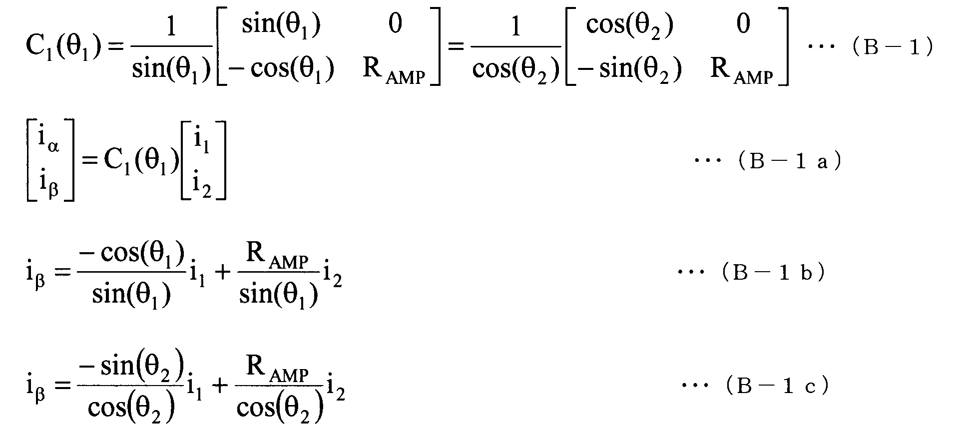
行列C1(θ1)は、例えば、θ1がπ/4であるときには式(B-2)によって表され、θ1がπ/3であるときには式(B-2a)によって表される。
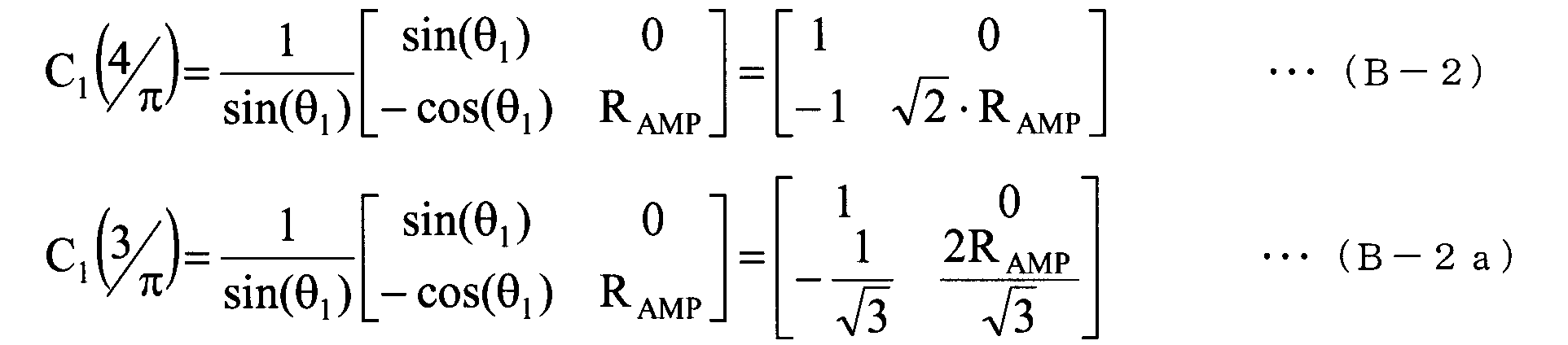
αβ座標系上の回転ベクトル630を角度θだけ回転させることで、PQ座標系上のベクトル630を得ることができる。αβ座標系上の回転ベクトル630を角度θだけ回転させるための行列C2(θ)は下記式(B-3)によって表され、行列C1(θ1)及びC2(θ)の積である行列C(θ)は下記式(B-4)によって表される。行列C(θ)を用いれば、信号i1及びi2を、PQ座標系上におけるベクトル630の直交2成分ip及びiqに変換することができる。即ち、i1及びi2とip及びiqとの間には、式(B-4a)が成立する。
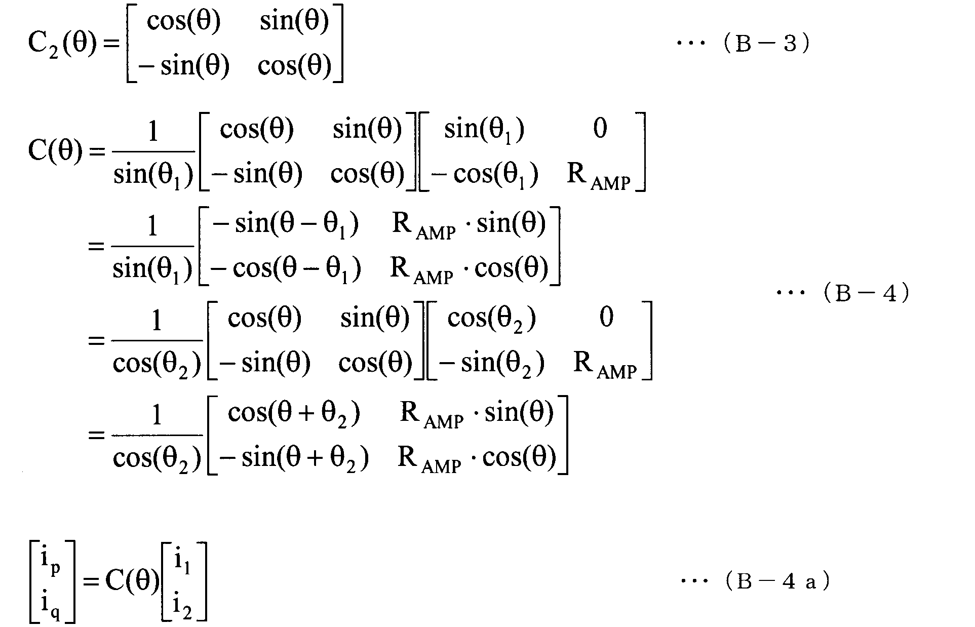
図15のフィルタ141は、フィルタリング対象信号の位相を遅らせる又は進ませるフィルタ処理をフィルタリング対象信号としての信号i1に施すことによりフィルタ信号i2を生成する。フィルタ141の伝達関数はF(s)で表される。フィルタ141において、周波数ωnにおける信号i1のゲインは1/RAMPである。従って、フィルタ141を通すことにより、信号i1における周波数ωnの信号成分の振幅は1/RAMPになる。
ベクトル成分算出部142は、θ1及びθを用いた上記式(B-4)及び(B-4a)に従う座標変換を行うことによって、信号i1及びi2から信号ip及びiqを算出する。ベクトル成分算出部142として、図17のベクトル成分算出部142Aを用いることも可能である。ベクトル成分算出部142Aには座標変換部143及び144が設けられている。座標変換部143は、θ1に基づき上記式(B-1)及び(B-1a)に従って信号i1及びi2から信号iα及びiβを算出する。座標変換部144は、座標変換部143にて算出された信号iα及びiβを要素とする行列に行列C2(θ)を乗じることにより信号ip及びiqを算出する。即ち、信号iα及びiβを直交二成分とする、αβ座標系上の回転ベクトル630を、行列C2(θ)を用いてθだけ回転させることにより、信号ip及びiqを直交二成分とする、PQ座標系上のベクトル630を算出する。実際には、算出部142及び座標変換部144においてθestがθとして用いられる。
算出部142によって求められた信号ip及びiqは、有効電流信号ip及び無効電流信号iqとして電流検出/推定部115から出力される。このように、座標変換部133は、ip及びiqを直交2成分として持つベクトル信号(ベクトル630を表す信号)を、電流センサ4の出力信号に基づいて生成するベクトル信号生成部として機能する。
信号i1及びi2間の位相差θ1がπ/4又はπ/3であるときを想定し、フィルタ141及びベクトル成分算出部142の具体的演算動作を説明する。但し、“0<|θ1|<π/2”が満たされる限り、θ1の値はπ/4及びπ/3以外であってもよい。電流検出/推定部115は、後述の各式を用いて各種信号を求めることができるが、この際、後述の各式におけるθとしてθestを用いることができる。
[θ1=π/4の場合の具体例]
信号i1及びi2間の位相差θ1がπ/4であるときにおけるフィルタ141及びベクトル成分算出部142の具体的演算動作を説明する。θ1=π/4であるとき、フィルタ141は、信号i1にフィルタ141の伝達関数“F(s)=2ωn/(s+ωn)”を作用させる下記式(B-5)に従ってフィルタ信号i2を生成する。式(B-5)のフィルタ信号i2は、信号i1からπ/4だけ位相が遅れた位相遅れ信号である。式(B-5)及び後述の幾つかの式に現われる演算記号“s”は、ラプラス演算子である。
信号i1及びi2間の位相差θ1がπ/4であるときにおけるフィルタ141及びベクトル成分算出部142の具体的演算動作を説明する。θ1=π/4であるとき、フィルタ141は、信号i1にフィルタ141の伝達関数“F(s)=2ωn/(s+ωn)”を作用させる下記式(B-5)に従ってフィルタ信号i2を生成する。式(B-5)のフィルタ信号i2は、信号i1からπ/4だけ位相が遅れた位相遅れ信号である。式(B-5)及び後述の幾つかの式に現われる演算記号“s”は、ラプラス演算子である。

上記式(B-1a)及び(B-2)に基づく下記式(B-6)により、信号i1及びi2をαβ座標系上の回転ベクトル630の直交2成分iα及びiβに変換することができる。ここで、信号i2の振幅が信号i1の振幅の√2倍となるように、式(B-5)に対応するフィルタ141のゲインは設定されている。即ち、RAMP=1/√2である。尚、“√2”は、2の正の平方根である。

式(B-6)で得られたiα及びiβを、下記式(B-7)により、PQ座標系上のベクトル630の直交2成分ip及びiqに変換することもできる。

式(B-6)を用いて一旦iα及びiβを算出してから式(B-7)によりip及びiqを算出するのではなく、下記式(B-8)を用いてi1及びi2から直接的にip及びiqを求めることもできる。

更に、本例の如く位相差θ1がπ/4の場合には、次式(B-9)を用いてi1及びi2から直接的にip及びiqを求めることもできる。

以上のように、一次のフィルタを用いた比較的簡単な演算によって、回転座標系上における単相のベクトル信号(直交2成分がip及びiqであるベクトル信号)を得ることができる。
上記式(B-5)に従って得られるフィルタ信号i2は信号i1に対してπ/4だけ位相が遅れているが、信号i1に対してπ/4だけ位相を進ませた信号をフィルタ信号i2として生成するようにしてもよく、この場合には、下記式(B-5a)に従ってフィルタ信号i2を生成すればよい。式(B-5a)のフィルタ信号i2は、信号i1からπ/4だけ位相が進んだ位相進み信号であり、式(B-5a)にてフィルタ信号i2を生成する場合、“θ1=-π/4”である。

また、フィルタ141において、式(B-5)の右辺にて表される信号の反転信号をフィルタ信号i2として生成するようにしても良い。任意の注目信号の反転信号とは、該注目信号の符号を反転した信号を指す。即ち例えば、信号i1の反転信号は(-i1)である。従って、式(B-5)の右辺にて表される信号の反転信号は“-(2ωni1/(s+ωn))”で表される。式(B-5)の右辺にて表される信号の反転信号は、信号i1に対して3π/4だけ位相が進んだ信号である。このように、一次のフィルタ141にて信号の位相をπ/2以上進めることもできる。同様に、フィルタ141において、式(B-5a)の右辺にて表される信号の反転信号(-(2si1/(s+ωn))をフィルタ信号i2として生成するようにしても良い。式(B-5a)の右辺にて表される信号の反転信号は、信号i1に対して3π/4だけ位相が遅れた信号である。このように、一次のフィルタ141にて信号の位相をπ/2以上遅らせることもできる。
[θ1=π/3の場合の具体例]
信号i1及びi2間の位相差θ1がπ/3であるときにおけるフィルタ141及びベクトル成分算出部142の具体的演算動作を説明する。θ1=π/3であるとき、フィルタ141は、信号i1にフィルタ141の伝達関数F(s)を作用させる下記式(B-10)に従ってフィルタ信号i2を生成する。式(B-10)のフィルタ信号i2は、信号i1からπ/3だけ位相が遅れた位相遅れ信号である。
信号i1及びi2間の位相差θ1がπ/3であるときにおけるフィルタ141及びベクトル成分算出部142の具体的演算動作を説明する。θ1=π/3であるとき、フィルタ141は、信号i1にフィルタ141の伝達関数F(s)を作用させる下記式(B-10)に従ってフィルタ信号i2を生成する。式(B-10)のフィルタ信号i2は、信号i1からπ/3だけ位相が遅れた位相遅れ信号である。

上記式(B-1a)及び(B-2a)に基づく下記式(B-11)により、信号i1及びi2をαβ座標系上の回転ベクトル630の直交2成分iα及びiβに変換することができる。ここで、信号i2の振幅が信号i1の振幅と同じになるように、式(B-10)に対応するフィルタ141のゲインは設定されている。即ち、RAMP=1である。

式(B-11)で得られたiα及びiβを、下記式(B-12)により、PQ座標系上のベクトル630の直交2成分ip及びiqに変換することもできる。

式(B-11)を用いて一旦iα及びiβを算出してから式(B-12)によりip及びiqを算出するのではなく、下記式(B-13)を用いてi1及びi2から直接的にip及びiqを求めることもできる。

以上のように、一次のフィルタを用いた比較的簡単な演算によって、回転座標系上における単相のベクトル信号(直交2成分がip及びiqであるベクトル信号)を得ることができる。
上記式(B-10)に従って得られるフィルタ信号i2は信号i1に対してπ/3だけ位相が遅れているが、信号i1に対してπ/3だけ位相を進ませた信号をフィルタ信号i2として生成するようにしてもよく、この場合には、下記式(B-10a)に従ってフィルタ信号i2を生成すればよい。式(B-10a)のフィルタ信号i2は、信号i1からπ/3だけ位相が進んだ位相進み信号であり、式(B-10a)にてフィルタ信号i2を生成する場合、“θ1=-π/3”である。

また、フィルタ141において、式(B-10)の右辺にて表される信号の反転信号をフィルタ信号i2として生成するようにしても良い。式(B-10)の右辺にて表される信号の反転信号は、信号i1に対して2π/3だけ位相が進んだ信号である。このように、一次のフィルタ141にて信号の位相をπ/2以上進めることもできる。同様に、フィルタ141において、式(B-10a)の右辺にて表される信号の反転信号をフィルタ信号i2として生成するようにしても良い。式(B-10a)の右辺にて表される信号の反転信号は、信号i1に対して2π/3だけ位相が遅れた信号である。このように、一次のフィルタ141にて信号の位相をπ/2以上遅らせることもできる。
図18の波形681~685は、夫々、検出構成K1又はK2を採用した場合における信号idc、idcS、ip、iq及びiSestの波形を表している。出力電圧vSのゼロクロス付近では電流センサ4による電流検出(出力電流iSの検出)ができないことが、波形682に現われている(図18では、検出不可期間におけるidcSがゼロであると仮定している)。検出不可期間において信号波形685に対応する推定信号iSestを利用することで、単相インバータ2に対する安定的な制御を維持することができる。
――推定ユニットの構成例――
図15の座標変換部133の技術を、図14の推定ユニット118に適用することもできる。図19に、この適用の成された推定ユニット118の構成例である推定ユニット118Aのブロック図を示す。推定ユニット118Aを、図14の推定ユニット118として用いることができる。推定ユニット118Aは、符号161~166によって参照される各部位を備える。
図15の座標変換部133の技術を、図14の推定ユニット118に適用することもできる。図19に、この適用の成された推定ユニット118の構成例である推定ユニット118Aのブロック図を示す。推定ユニット118Aを、図14の推定ユニット118として用いることができる。推定ユニット118Aは、符号161~166によって参照される各部位を備える。
推定ユニット118Aには、図14のBPF117からの信号vS’が単相信号として入力され、信号vS’が信号v1として取り扱われる。フィルタ161は、フィルタリング対象信号の位相を遅らせる又は進ませるフィルタ処理をフィルタリング対象信号としての信号v1に施すことによりフィルタ信号v2を生成する。信号v1及びv2は、
v1=AMPv1・cos(θv1)、
v2=AMPv2・cos(θv2)、
によって表される。
v1=AMPv1・cos(θv1)、
v2=AMPv2・cos(θv2)、
によって表される。
図15のフィルタ141におけるフィルタ処理及びベクトル成分算出部142における演算処理が、フィルタ161におけるフィルタ処理及びベクトル成分算出部162における演算処理に適用される。但し、この適用の際、上述のAMPi1、AMPi2、θi1、θi2、i1、i2、ip及びiqは、それぞれAMPv1、AMPv2、θv1、θv2、v1、v2、vp及びvqに読み替えられる。算出部162は、算出部142と同様にして、信号v1及びv2から信号vp及びvqを算出する。この際、算出部162において、積分部166にて求められたθestがθとして用いられる。vp及びvqは、夫々、出力電圧vSのP軸成分及びQ軸成分を表す。
位相差算出部163は、ベクトル成分算出部162にて算出されたvp及びvqから、θと単相信号v1の位相θv1との間の位相差Δθを、次式(C-1)に従って求める。

推定ユニット118Aでは、Δθをゼロに収束させるための下記式(C-2)及び(C-3)に従うPLL(Phase Locked Loop)を構成することにより、θestをθv1に一致させる。KP及びKiは、夫々、PI制御部164にて実行される比例積分制御の比例係数及び積分係数である。

具体的には、位相差算出部163にて算出されたΔθと既知の角周波数として与えられたωnとに基づき、PI制御部164及び加算部165にて、式(C-2)に従い周波数ωestを算出する。積分部166は、式(C-3)に従い、算出された周波数ωestを積分することにより位相θestを算出する。推定ユニット118Aでは、座標変換における位相θ(=θest)と信号v1の位相θv1との間の位相差Δθがゼロに収束するようにPLLが構成されているため、位相θestは、位相θv1の推定値として機能する。従って、位相θv1の推定値θestの元となる周波数ωestは、単相信号v1の角周波数の推定値に相当する。例えば、単相信号v1の周波数は、既知の公称周波数ωn(例えば、60×2π)としてシステムに与えられるが、実際の単相信号v1の周波数(例えば、59.5×2π)は公称周波数ωnからずれることも多い。推定ユニット118Aによれば、単相信号v1の真の周波数を周波数ωestとして推定することができる。
また、Δθがゼロである場合、PQ座標系は単相信号v1の周波数と完全に同期して回転すると共に単相信号v1はQ軸成分を持たない。即ち、Δθがゼロであるとき、単相信号v1は、P軸成分のみを持つP軸上の信号となる。故に、算出部162にて算出される信号vpの値は、単相信号v1の振幅を表すこととなる。推定ユニット118Aでは、算出部162にて算出される信号vpの値を振幅AMPestとして出力する。上述の説明から明らかなように、振幅AMPestは、単相信号v1の振幅(即ち、信号v1の振幅AMPv1)の推定値を表している。
<<第3実施形態>>
本発明の第3実施形態を説明する。第3実施形態は、第1及び第2実施形態を基礎とする実施形態であり、第3実施形態において特に述べない事項に関しては、矛盾無き限り、第1及び第2実施形態の記載が第3実施形態に適用される。図20は、第1実施形態に係る電力変換システムの具体例である、第3実施形態に係る系統連系システムの概略構成図である。図20では下側検出構成K1が採用されているが、第3実施形態に係る系統連系システムに、検出構成J1、J2又はK2を採用しても良い(図1(a)、図2又は図9参照)。図20のインバータ制御回路(制御装置)203は、第1実施形態に係るインバータ制御回路3の具体例であり、制御回路3にて実現される任意の機能を実現可能である。制御回路203における任意の部位は、制御回路203にて得られた任意の情報(信号、指令値、検出値、推定値等)を自由に利用することができる。
本発明の第3実施形態を説明する。第3実施形態は、第1及び第2実施形態を基礎とする実施形態であり、第3実施形態において特に述べない事項に関しては、矛盾無き限り、第1及び第2実施形態の記載が第3実施形態に適用される。図20は、第1実施形態に係る電力変換システムの具体例である、第3実施形態に係る系統連系システムの概略構成図である。図20では下側検出構成K1が採用されているが、第3実施形態に係る系統連系システムに、検出構成J1、J2又はK2を採用しても良い(図1(a)、図2又は図9参照)。図20のインバータ制御回路(制御装置)203は、第1実施形態に係るインバータ制御回路3の具体例であり、制御回路3にて実現される任意の機能を実現可能である。制御回路203における任意の部位は、制御回路203にて得られた任意の情報(信号、指令値、検出値、推定値等)を自由に利用することができる。
第3実施形態に係る系統連系システムは、直流電源1、単相インバータ2、電流センサ4、電圧検出センサ6、電圧検出センサ7及び直流電圧保持部Cdを有すると共に、負荷55及び電力系統50に接続され、それらの接続関係は第2実施形態で述べたとおりである。第3実施形態に係る系統連系システムには、単相インバータ2を制御するインバータ制御回路203が設けられている。制御回路203には、符号111、115~119及び212~214によって参照される各部位が備えられている。即ち、図14の制御回路103から符号112~114にて参照される各部位を削除した後、代わりに符号212~214にて参照される各部位を制御回路103に設けることで制御回路203が得られる。図20の系統連系システムには、系統連系装置が内在している。系統連系装置は、制御回路203を備え、更に、直流電源1、単相インバータ2、電流センサ4、電圧検出センサ6及び電圧検出センサ7の内、少なくとも1つを更に備えうる。その他、図20に示される任意の部位が系統連系装置の構成要素に含まれる、と捉えることも可能である。
制御回路203における直流電圧制御部111、電流検出/推定部115、PWM回路116、BPF117、推定ユニット118及び単独運転検出部119の構成及び動作は、第2実施形態で述べたそれらと同様である。但し、制御回路203における電流検出/推定部115は、信号ip及びiqの代わりに、電流検出/推定部115によって検出又は推定された出力電流値iSを表す信号iSDを出力する(図15参照)。
電流指令生成部212は、推定ユニット118からの推定値θestに基づいて、制御部111からの有効電流指令値ip
*を出力電流指令値iS
*に変換する。指令値iS
*は、出力電流iSの目標値として機能する正弦波電流指令値である。有効電流制御部213は、信号iSDの値が指令値iS
*と一致するように、比例積分制御などを用いて電圧指令値vSO
*を算出する。指令値vSO
*は、(iSD-iS
*)をゼロにするために出力電圧vSに追加すべき電圧量を表す。加算部214は、BPF117からの信号値vS’に指令値vSO
*を加算することで(即ち“vS
*=(vSO
*+vS’)”に従って)電圧指令値vS
*を求め、求めた電圧指令値vS
*をPWM回路116に与える。
尚、検出された電圧信号vS’を加算部214に与える代わりに、θestを用いて生成した電圧信号vS’’を加算部214に与えるようにしてもよい。即ち、加算部214は、vS
*=(vSO
*+vS’’)に従って電圧指令値vS
*を求めてもよい。vS’’は、θestと既知の公称電圧値(例えば200ボルト)から求めた、出力電圧vSの推定値である。加算部214は有効電流制御部213の構成要素に含まれている、と考えることも可能である。
<<第4実施形態>>
本発明の第4実施形態を説明する。第4実施形態は第1実施形態を基礎とする実施形態であり、第4実施形態において特に述べない事項に関しては、第1実施形態の記載が第4実施形態にも適用される。第4実施形態に係る電力変換システムの概略構成図は、図1(a)又は図2と同じである。従って、第4実施形態に係る電力変換システムは、第1実施形態と同様、符号1~10及びCdによって参照される各部位を備え、第4実施形態に係る電力変換システムでは、下側検出構成J1又は上側検出構成J2が採用される。但し、第4実施形態及び後述の第5~第7実施形態では、特に記述なき限り、電力変換システムに下側検出構成J1が採用されていることを想定する。
本発明の第4実施形態を説明する。第4実施形態は第1実施形態を基礎とする実施形態であり、第4実施形態において特に述べない事項に関しては、第1実施形態の記載が第4実施形態にも適用される。第4実施形態に係る電力変換システムの概略構成図は、図1(a)又は図2と同じである。従って、第4実施形態に係る電力変換システムは、第1実施形態と同様、符号1~10及びCdによって参照される各部位を備え、第4実施形態に係る電力変換システムでは、下側検出構成J1又は上側検出構成J2が採用される。但し、第4実施形態及び後述の第5~第7実施形態では、特に記述なき限り、電力変換システムに下側検出構成J1が採用されていることを想定する。
既に述べたように、下側検出構成J1が採用された場合、区間IIにおいて対象電流値idcが出力電流値iSと一致する(図6(b)参照)。このため、制御回路3に設けられた電流検出部12は、vS
*の如何に関わらず、区間IIにおいて電流センサ4の出力信号をサンプリングすることにより、対象電流値idcを出力電流値iSとして検出することができる。第4実施形態に係る制御回路3は、電流検出部12による出力電流iSの検出結果に基づきアームSW1~SW4のオン期間を定めるパルス幅を決定することでインバータ2を制御する。
vS
*>0の場合においては、区間IIだけでなく、区間I及びIIIにおいても出力電流iSが電流センサ4に流れる(図6(a)及び(b)参照)。故に、vS
*>0の場合、電流センサ4の出力信号から出力電流iSを検出することに対する時間的制約は比較的緩い。一方、vS
*<0の場合においては、区間IIにおいてのみ出力電流iSが電流センサ4に流れるため、上記の時間的制約は比較的厳しくなる。vS
*<0の場合において区間IIの長さ(即ち、アームSW4のオン期間を定めるパルス幅)が所定の基準時間LTHより短くなると、サンプリングに必要なA/D変換時間やリンギング(スイッチングに由来して生じる電流脈動)の収束時間を確保できなくなり、結果、電流センサ4の出力信号から出力電流iSを検出することができなくなる。
そこで、第4実施形態に係る制御回路3は、電流センサ4の出力信号から出力電流iSが検出不能になることを防止するための機能、又は、電流センサ4の出力信号から出力電流iSが検出不能になる期間において出力電流iSを推定する機能を備える。前者の機能を実現する処理の例として、以下に第1及び第2特殊処理を示し、後者の機能を実現する処理を電流推定処理と呼ぶ。第1実施形態で述べたように、アームSW4のオン期間を定めるパルス幅を、パルス幅ONSW4と表記する。同様に、アームSW1~SW3のオン期間を定めるパルス幅を、夫々、パルス幅ONSW1~ONSW3と表記する。
――第1特殊処理――
第1特殊処理を説明する。第1特殊処理において、制御回路3は、各キャリア周期においてパルス幅ONSW4が基準時間LTH以上確保されるように、パルス幅ONSW4に制限を設ける(具体的には下限を設ける)。即ち、第1特殊処理は、パルス幅ONSW4の制限によって、各キャリア周期においてパルス幅ONSW4を基準時間LTH以上確保する処理である。第1特殊処理により、各キャリア周期において常にパルス幅ONSW4が基準時間LTHを下回らないため、電流検出部12は、各キャリア周期において常に区間II中の電流センサ4の出力信号から出力電流iSを検出することが可能となる。基準時間LTHを、実験等を介して予め定めておくことができる。尚、下アームSW4がオンのとき上アームSW3はオフであるから、パルス幅ONSW4に下限を設けることは、パルス幅ONSW3に上限を設けることと等価であり、そのような上限及び下限を設ければ、出力電圧vSの可変範囲に制限が加わる。
第1特殊処理を説明する。第1特殊処理において、制御回路3は、各キャリア周期においてパルス幅ONSW4が基準時間LTH以上確保されるように、パルス幅ONSW4に制限を設ける(具体的には下限を設ける)。即ち、第1特殊処理は、パルス幅ONSW4の制限によって、各キャリア周期においてパルス幅ONSW4を基準時間LTH以上確保する処理である。第1特殊処理により、各キャリア周期において常にパルス幅ONSW4が基準時間LTHを下回らないため、電流検出部12は、各キャリア周期において常に区間II中の電流センサ4の出力信号から出力電流iSを検出することが可能となる。基準時間LTHを、実験等を介して予め定めておくことができる。尚、下アームSW4がオンのとき上アームSW3はオフであるから、パルス幅ONSW4に下限を設けることは、パルス幅ONSW3に上限を設けることと等価であり、そのような上限及び下限を設ければ、出力電圧vSの可変範囲に制限が加わる。
上側検出構成J2の採用時における第1特殊処理について説明する。上側検出構成J2が採用されている場合、電流検出部12は、区間IVにおいて電流センサ4の出力信号をサンプリングすることにより、対象電流値idcを出力電流値iSとして検出することができる。より具体的には、上側検出構成J2が採用されている場合、電流検出部12は、各キャリア周期において、キャリア信号値CSVALが極小値をとるタイミングに電流センサ4の出力信号をサンプリングすることにより、キャリア信号値CSVALが極小値をとるタイミングにおける対象電流値idcを出力電流値iSとして検出することができる。vS
*<0の場合(図7(a)~(c)参照)、区間IVだけでなく区間I及びIIIにおいても出力電流iSが図2の電流センサ4に流れるため上記時間的制約は比較的緩いが、vS
*>0の場合においては(図6(a)~(c)参照)、
区間IVにおいてのみ出力電流iSが図2の電流センサ4に流れるため上記時間的制約は比較的厳しくなる。
区間IVにおいてのみ出力電流iSが図2の電流センサ4に流れるため上記時間的制約は比較的厳しくなる。
故に、上側検出構成J2が採用されている場合、第1特殊処理において、制御回路3は、各キャリア周期においてパルス幅ONSW3が基準時間LTH以上確保されるように、パルス幅ONSW3に制限を設ける(具体的には下限を設ける)。結果、各キャリア周期において常にパルス幅ONSW3が基準時間LTHを下回らないため、電流検出部12は、各キャリア周期において常に区間IV中の図2の電流センサ4の出力信号から出力電流iSを検出することが可能となる。パルス幅ONSW3に下限を設けることは、パルス幅ONSW4に上限を設けることと等価であり、そのような上限及び下限を設ければ、出力電圧vSの可変範囲に制限が加わる。
以下の説明では、説明の便宜上、下側検出構成J1の採用時におけるパルス幅ONSW4及び上側検出構成J2の採用時におけるパルス幅ONSW3の夫々を、対象パルス幅と呼ぶ。また、第1実施形態で述べたように、出力電流iSの検出を行うために電流センサ4の出力信号のサンプリングを行うべきタイミングを対象タイミングと呼ぶ。対象タイミングは、下側検出構成J1の採用時においてはキャリア信号値CSVALが極大値をとるタイミングであり、上側検出構成J2の採用時においてはキャリア信号値CSVALが極小値をとるタイミングである。
下側検出構成J1及び上側検出構成J2の何れが採用された場合においても、制御回路3は、例えば、インバータ2の出力電圧vSの目標値である電圧指令値vS
*又は電圧指令値vS
*に基づく電圧指令値vSB
*(図4又は図5参照)に制限を加えることで(出力電圧vSの振幅に上限を設けることで)、第1特殊処理を実現することができる。図22(a)に示す如く、第1特殊処理を実行するパルス幅制限部31が制御回路3に設けられていると考えることができる。
――第2特殊処理――
第2特殊処理を説明する。第2特殊処理も、各キャリア周期において対象パルス幅を基準時間LTH以上確保する処理である。但し、第1特殊処理では当該確保がパルス幅制限によって実現されるのに対し、第2特殊処理では、当該確保がキャリア周期又はキャリア周波数の制御によって実現される。即ち、第2特殊処理において、制御回路3は、各キャリア周期において対象パルス幅が基準時間LTH以上確保されるように、キャリア周期を制御する(キャリア周波数を制御する)。キャリア周波数は、キャリア信号CSの周波数であり、キャリア周期の逆数である。従って、キャリア周期の制御又は変更等は、キャリア周波数の制御又は変更等と等価である。キャリア周期の制御、拡大、縮小又は変更等は、キャリア周期の時間長さの制御、拡大、縮小又は変更等を意味する。図22(b)に示す如く、第2特殊処理を実行するキャリア制御部32が、制御回路3(例えばPWM回路11)に設けられていると考えることができる。
第2特殊処理を説明する。第2特殊処理も、各キャリア周期において対象パルス幅を基準時間LTH以上確保する処理である。但し、第1特殊処理では当該確保がパルス幅制限によって実現されるのに対し、第2特殊処理では、当該確保がキャリア周期又はキャリア周波数の制御によって実現される。即ち、第2特殊処理において、制御回路3は、各キャリア周期において対象パルス幅が基準時間LTH以上確保されるように、キャリア周期を制御する(キャリア周波数を制御する)。キャリア周波数は、キャリア信号CSの周波数であり、キャリア周期の逆数である。従って、キャリア周期の制御又は変更等は、キャリア周波数の制御又は変更等と等価である。キャリア周期の制御、拡大、縮小又は変更等は、キャリア周期の時間長さの制御、拡大、縮小又は変更等を意味する。図22(b)に示す如く、第2特殊処理を実行するキャリア制御部32が、制御回路3(例えばPWM回路11)に設けられていると考えることができる。
図23を参照して、具体的にキャリア周期の制御方法を説明する。キャリア周期を記号PCRにて表す。図23は、キャリア周期PCRを制御するキャリア制御部32の動作フローチャートである。PWM回路11は、ステップS11~S17の実行中に定められたキャリア周期PCRを持つキャリア信号CSを生成し、上述の方法に従って、各アームに対するPWM信号を生成する。
まずステップS11において、キャリア制御部32は、キャリア周期PCRに所定の基準周期PCRREFを設定する。続くステップS12において、キャリア制御部32は電流検出可否判定処理を行う。キャリア制御部32によって実行される電流検出可否判定処理は、第1実施形態で述べたそれと同様のものであって良い。上述したように、電流検出可否判定処理は、現時点が検出可能期間と検出不可期間の何れに属するのかを判定する処理である。説明の具体化のため、この判定を成すタイミングを注目タイミングと呼ぶ。尚、電流検出可否判定処理は、後述のスイッチ部132B(図27参照)においても実行される。
電流検出可否判定処理において、キャリア制御部32又はスイッチ部132Bは、注目タイミングにおける電圧指令値vS
*(又は、注目タイミングにおける電圧指令値vS
*の元になる値)と、注目タイミングにおけるキャリア周期PCR(又はキャリア周波数)とに基づき、注目タイミングにおける電圧指令値vS
*及びキャリア周期PCRを用いたときに得られるべき対象パルス幅を、判定パルス幅として求める。そして、キャリア制御部32又はスイッチ部132Bは、判定パルス幅が基準時間LTH以上であるならば注目タイミングは検出可能期間に属していると判断することができ、判定パルス幅が基準時間LTH未満であるならば注目タイミングは検出不可期間に属していると判断することができる。
電流検出可否判定処理の結果は、ステップS13に利用される。注目タイミングが検出不可期間に属している場合には、ステップS13からステップS14への移行が発生し、注目タイミングが検出可能期間に属している場合には、ステップS13からステップS15への移行が発生する。
ステップS14において、キャリア制御部32は、注目タイミングが検出可能期間に属するようにキャリア周期PCRを拡大し(即ち、キャリア周波数を減少させ)、その後、ステップS12に戻る。キャリア周期PCRに上限を設けておくようにしても良い。この場合、第1特殊処理を組み合わせて実行しても良い。即ち例えば、キャリア周期PCRを上限の周期に設定しても注目タイミングが検出不可期間に属すると判断される場合、第1特殊処理によるパルス幅制限によって対象パルス幅を基準時間LTH以上確保するようにしてもよい。
ステップS15において、“PCR>PCRREF”の成否が判定される。そして、注目タイミングにおけるキャリア周期PCRが基準周期PCRREFよりも大きければステップS15からステップS16への移行が発生し、そうでなければ、ステップS12に戻る。ステップS16において、キャリア制御部32は、注目タイミングにおける電圧指令値vS
*及びキャリア周期PCRに基づき、注目タイミングが検出可能期間に属するという条件を満たしたままキャリア周期PCRを縮小可能か否かを判断する。縮小不可と判断した場合にはステップS16からステップS12に直接戻るが、縮小可能と判断した場合には、ステップS17においてキャリア周期PCRを縮小してから(即ち、キャリア周波数を増大させてから)ステップS12に戻る。ステップS17におけるキャリア周期PCRの縮小は、注目タイミングが検出可能期間に属するという条件を満たした上で実行され、縮小後のキャリア周期PCRの下限は基準周期PCRREFである。
上述したような第2特殊処理によれば、或いは、第1及び第2特殊処理の組み合わせによれば、各キャリア周期において常に対象パルス幅が基準時間LTHを下回らないため、電流検出部12は、各キャリア周期において常に電流センサ4の出力信号から出力電流iSを検出することが可能となる。また、第1特殊処理によるパルス幅制限は出力電圧vSの可変範囲の縮小を招くが、第2特殊処理を用いれば、このような縮小は無くなる又は軽減される。
――電流推定処理――
電流推定処理では、パルス幅の制限等を設けず、注目タイミングが検出不可期間である場合に、過去の検出電流情報を用いて出力電流iSを推定する。電流推定処理を利用すれば、パルス幅制限に起因する、出力電圧vSの可変範囲縮小を回避することができる。本実施形態に係る電流推定処理の方法は、上述の何れかの実施形態で述べたそれと同じであっても良い。電流推定処理の内容は、後述の他の実施形態においても詳説される。
電流推定処理では、パルス幅の制限等を設けず、注目タイミングが検出不可期間である場合に、過去の検出電流情報を用いて出力電流iSを推定する。電流推定処理を利用すれば、パルス幅制限に起因する、出力電圧vSの可変範囲縮小を回避することができる。本実施形態に係る電流推定処理の方法は、上述の何れかの実施形態で述べたそれと同じであっても良い。電流推定処理の内容は、後述の他の実施形態においても詳説される。
何れにせよ、本実施形態(及び後述の各実施形態)では、電流センサを比較的安価なシャント抵抗にて形成することができ且つ単一の電流センサにて単相インバータの出力電流検出が可能となるため、図21の構成及び国際公開WO2007/083486号パンフレットに記載の構成と比べて、システム全体のコストを削減することが可能となる。電流センサを1つにまで削減したことに伴って生じうる問題は、第1特殊処理、第2特殊処理又は電流推定処理により解決できる。特に、第2特殊処理又は電流推定処理を用いた場合には、第1特殊処理を用いた場合と比べて、出力電圧vSの可変範囲を拡大することができる。
出力電圧vSの上限設定などで実現される第1特殊処理は、上記第2従来方法では発生するような電流波形歪みを伴わないし、第2特殊処理及び電流推定処理も、当然、そのような電流波形歪みを伴わない。故に、本実施形態の技術を系統連系に利用した場合、系統連系に関するガイドラインの基準を満たしやすくなる(本実施形態の技術を系統連系に利用した具体的構成は、他の実施形態にて後述される)。
<<第5実施形態>>
本発明の第5実施形態を説明する。第5実施形態は、第1、第2及び第4実施形態を基礎とする実施形態であり、第5実施形態において特に述べない事項に関しては、矛盾無き限り、第1、第2及び第4実施形態の記載が第5実施形態に適用される。図24は、第1又は第4実施形態に係る電力変換システムの具体例である、第5実施形態に係る系統連系システムの概略構成図である。図24では下側検出構成J1が採用されているが、第5実施形態に係る系統連系システムに上側検出構成J2を採用しても良い。
本発明の第5実施形態を説明する。第5実施形態は、第1、第2及び第4実施形態を基礎とする実施形態であり、第5実施形態において特に述べない事項に関しては、矛盾無き限り、第1、第2及び第4実施形態の記載が第5実施形態に適用される。図24は、第1又は第4実施形態に係る電力変換システムの具体例である、第5実施形態に係る系統連系システムの概略構成図である。図24では下側検出構成J1が採用されているが、第5実施形態に係る系統連系システムに上側検出構成J2を採用しても良い。
図24のPWM回路116及び電流検出部115Aは、夫々、図1(a)のPWM回路11及び電流検出部12が実現する機能と同等の機能を実現する。図24のインバータ制御回路(制御装置)103Aは、図1(a)のインバータ制御回路3の具体例であり、制御回路3にて実現される任意の機能を実現可能である。制御回路103Aにおける任意の部位は、制御回路103Aにて得られた任意の情報(信号、指令値、検出値、推定値等)を自由に利用することができる。第5実施形態では、第1及び第2特殊処理の何れか一方が実行されることで、各キャリア周期において常に対象パルス幅が基準時間LTH以上になっているものとする。
第5実施形態に係る系統連系システムは、第1又は第4実施形態で述べた直流電源1、単相インバータ2、電流センサ4、電圧検出センサ6、電圧検出センサ7及び直流電圧保持部Cdを有すると共に、単相インバータ2を制御するインバータ制御回路103Aを有し、負荷55と単相の交流電力を出力する電力系統50とに接続されている。制御回路103Aには、符号111~114、115A及び116~119によって参照される各部位が備えられている。図24の系統連系システムには、系統連系装置が内在している。系統連系装置は、制御回路103Aを備え、更に、直流電源1、単相インバータ2、電流センサ4、電圧検出センサ6及び電圧検出センサ7の内、少なくとも1つを更に備えうる。その他、図24に示される任意の部位が系統連系装置の構成要素に含まれる、と捉えることも可能である。
制御回路103Aにおいて符号111~114及び116~119によって参照される各部位の構成及び動作は、第2実施形態(図14参照)で述べたそれらと同じである。従って例えば、図24の推定ユニット118として、図19の推定ユニット118Aを用いることもできる。以下、第2実施形態に係る系統連系システム(図14)と第5実施形態に係る系統連系システム(図24)との相違点に特に注目し、相違点に注目した説明を行う。第5実施形態において特に述べない事項に関しては、矛盾無き限り、第2実施形態の記載を第5実施形態に適用することができるが、この適用の際、第2実施形態における“制御回路103”及び“電流検出/推定部115”は、夫々、第5実施形態において“制御回路103A”及び“電流検出部115A”に読み替えられる。
電流センサ4は、検出した対象電流idcの電流値を表す信号、即ち対象電流信号idcを電流検出部115Aに伝達する。電流検出部115Aは、各キャリア周期において、対象タイミングで電流センサ4の出力信号をサンプリングすることにより、対象タイミングにおける対象電流値idcを出力電流値iSとして検出する。図24の系統連系システムでは下側検出構成J1が採用されているため、対象タイミングはキャリア信号値CSVALが極大値をとるタイミングである。系統連系システムに上側検出構成J2を採用した場合においては、対象タイミングはキャリア信号値CSVALが極小値をとるタイミングである。
単相インバータ2の出力電流は有効電流と無効電流から形成される。電流検出部115Aは、図14の電流検出/推定部115と同様、座標変換部としての機能も有し、推定ユニット118からの位相θestに基づき、検出した出力電流iSから出力電流iSを形成する有効電流及び無効電流を算出し、有効電流の電流値を信号値として有する有効電流信号ip及び無効電流の電流値を信号値として有する無効電流信号iqを生成する。
上述したように、第5実施形態では、第1及び第2特殊処理の何れか一方が実行される。このため、制御回路103Aには、パルス幅制限部31及びキャリア制御部32の少なくとも一方が含まれていると考えることができる(図22(a)及び(b)参照)。
制御回路103Aにパルス幅制限部31を含める場合の動作について説明を加える。出力電圧vSの振幅に上限を設けることで対象パルス幅に制限を加えることができる。このため、パルス幅制限部31は、出力電圧vSの振幅が所定の上限振幅を上回らないように電圧指令値vS
*に制限を設け、これによって、第1特殊処理における対象パルス幅の制限を実現しても良い。
一方、出力電圧vSが一定であっても直流電圧Edが変化すれば対象パルス幅(図24の構成においてパルス幅ONSW4)は変化する。即ち、出力電圧vSが一定であっても、直流電圧Edが比較的高ければパルス幅ONSW4は比較的長くなり、直流電圧Edが比較的低ければパルス幅ONSW4は比較的短くなる。このため、パルス幅制限部31は、電圧指令値vS
*ではなく指令値Ed
*に制限を設けても良い。即ち、パルス幅制限部31は、指令値Ed
*が所定の下限値を下回らないように指令値Ed
*に制限を設け、これによって、第1特殊処理における対象パルス幅の制限を実現しても良い。例えば、太陽電池の動作電圧が低い場合や、太陽電池の内部抵抗における電圧降下の増大により直流電圧Edが低くなった場合などにおいて、上述の指令値Ed
*の制限を実行すると良い。直流電源1が蓄電池である場合も同様である。即ち例えば、蓄電池の残量が少なくなって蓄電池の動作電圧(蓄電池の出力電圧)が低くなった場合や、蓄電池の内部抵抗における電圧降下の増大により直流電圧Edが低くなった場合などにおいて、上述の指令値Ed
*の制限を実行すると良い。
太陽電池又は蓄電池の出力電力の増大は、太陽電池又は蓄電池の内部抵抗における電圧降下の増大を招く。一方で、太陽電池又は蓄電池の出力電力の増大は、指令値ip
*の増大に相当する。このため、パルス幅制限部31は、指令値vS
*及びEd
*ではなく指令値ip
*に制限を設けても良い。即ち、パルス幅制限部31は、指令値ip
*が所定の上限値を上回らないように指令値ip
*に制限を設け、これによって、第1特殊処理における対象パルス幅の制限を実現しても良い。
指令値vS
*、Ed
*又はip
*に制限を設けることは、第1特殊処理における対象パルス幅の制限を実現するための手段であると考えることができる。対象パルス幅の制限を実現するために成すことのできる、電圧指令値vS
*に対する制限は、インバータ2の出力電力(又は出力電圧)に対する制限に属し、電流指令値ip
*に対する制限は、インバータ2の出力電力(又は出力電流)に対する制限に属し、指令値Ed
*に対する制限は、直流電源1の出力電圧に対する制限に属する。これらの制限は、上記第2従来方法では発生するような電流波形歪みを伴わない。
――電流検出部の構成例――
次に、電流検出部115Aの内部構成例を説明する。図25は、電流検出部115Aの内部ブロック図の例である。図25の電流検出部115Aは、符号131、132A及び133によって参照される各部位を備える。
次に、電流検出部115Aの内部構成例を説明する。図25は、電流検出部115Aの内部ブロック図の例である。図25の電流検出部115Aは、符号131、132A及び133によって参照される各部位を備える。
図25のA/D変換部131は、図15のそれと同じものである。従って、図25のA/D変換部131は、各キャリア周期において、対象タイミングに電流センサ4の出力信号をサンプリングする。サンプリングされた電流センサ4の出力信号の値、即ち、サンプリングされた対象電流値idcを、記号idcSにて表す。スイッチ部132Aは、電流値idcSを信号値として有する信号を信号iSDとして出力する。即ち、第5実施形態において、信号idcSと信号iSDは全く同じものである。スイッチ部132Aは、第5実施形態と後述の第7実施形態(図27参照)との関係を分かり易くするために便宜上導入されたものであり、実際には、スイッチ部132Aは割愛可能である。
信号iSDの値は、電流検出部115Aによって検出された出力電流値iSに相当する。信号iSDは、単相信号として、フィルタ141及びベクトル成分算出部142から成る座標変換部133に入力される。図25に示される記号i1(=iSD)及びi2の意義は、第2実施形態で述べた通りである。図25の座標変換部133は、図15のそれと同じものであり、図25のフィルタ141及びベクトル成分算出部142にて実行可能な具体的演算動作も、第2実施形態で述べたものと同様である。図25のベクトル成分算出部142として、図17のベクトル成分算出部142Aを用いることもできる。算出部142によって求められた信号ip及びiqは、有効電流信号ip及び無効電流信号iqとして電流検出部115Aから出力される。第2実施形態でも述べたように、座標変換部133は、ip及びiqを直交2成分として持つベクトル信号(図16(a)のベクトル630を表す信号)を、電流センサ4の出力信号に基づいて生成するベクトル信号生成部として機能する。
<<第6実施形態>>
本発明の第6実施形態を説明する。第6実施形態は、第1~第5実施形態を基礎とする実施形態であり、第6実施形態において特に述べない事項に関しては、矛盾無き限り、第1~第5実施形態の記載が第6実施形態に適用される。図26は、第1又は第4実施形態に係る電力変換システムの具体例である、第6実施形態に係る系統連系システムの概略構成図である。図26では下側検出構成J1が採用されているが、第6実施形態に係る系統連系システムに上側検出構成J2を採用しても良い。図26のインバータ制御回路(制御装置)203Aは、図1(a)のインバータ制御回路3の具体例であり、制御回路3にて実現される任意の機能を実現可能である。制御回路203Aにおける任意の部位は、制御回路203Aにて得られた任意の情報(信号、指令値、検出値、推定値等)を自由に利用することができる。第6実施形態では、第1及び第2特殊処理の何れか一方が実行されることで、各キャリア周期において常に対象パルス幅が基準時間LTH以上になっているものとする。このため、制御回路203Aには、パルス幅制限部31及びキャリア制御部32の少なくとも一方が含まれていると考えることができる(図22(a)及び(b)参照)。
本発明の第6実施形態を説明する。第6実施形態は、第1~第5実施形態を基礎とする実施形態であり、第6実施形態において特に述べない事項に関しては、矛盾無き限り、第1~第5実施形態の記載が第6実施形態に適用される。図26は、第1又は第4実施形態に係る電力変換システムの具体例である、第6実施形態に係る系統連系システムの概略構成図である。図26では下側検出構成J1が採用されているが、第6実施形態に係る系統連系システムに上側検出構成J2を採用しても良い。図26のインバータ制御回路(制御装置)203Aは、図1(a)のインバータ制御回路3の具体例であり、制御回路3にて実現される任意の機能を実現可能である。制御回路203Aにおける任意の部位は、制御回路203Aにて得られた任意の情報(信号、指令値、検出値、推定値等)を自由に利用することができる。第6実施形態では、第1及び第2特殊処理の何れか一方が実行されることで、各キャリア周期において常に対象パルス幅が基準時間LTH以上になっているものとする。このため、制御回路203Aには、パルス幅制限部31及びキャリア制御部32の少なくとも一方が含まれていると考えることができる(図22(a)及び(b)参照)。
第6実施形態に係る系統連系システムは、直流電源1、単相インバータ2、電流センサ4、電圧検出センサ6、電圧検出センサ7及び直流電圧保持部Cdを有すると共に、負荷55及び電力系統50に接続され、それらの接続関係は第1~第5実施形態で述べたとおりである。第6実施形態に係る系統連系システムには、単相インバータ2を制御するインバータ制御回路203Aが設けられている。制御回路203Aには、符号111、115A、116~119及び212~214によって参照される各部位が備えられている。即ち、図24の制御回路103Aから符号112~114にて参照される各部位を削除した後、代わりに符号212~214にて参照される各部位を制御回路103Aに設けることで制御回路203Aが得られる。図26の系統連系システムには、系統連系装置が内在している。系統連系装置は、制御回路203Aを備え、更に、直流電源1、単相インバータ2、電流センサ4、電圧検出センサ6及び電圧検出センサ7の内、少なくとも1つを更に備えうる。その他、図26に示される任意の部位が系統連系装置の構成要素に含まれる、と捉えることも可能である。
制御回路203Aにおける電流検出部115Aの構成及び動作は、第5実施形態で述べたそれらと同様である。但し、制御回路203Aにおける電流検出部115Aは、第3実施形態に係る電流検出/推定部115(図20参照)と同様、信号ip及びiqの代わりに、電流検出部115Aによって検出された出力電流値iSを表す信号iSDを出力する(図25も参照)。電流検出部115Aを除き、制御回路203Aの内部構成及び動作は、図20の制御回路203のそれらと同様である。
<<第7実施形態>>
本発明の第7実施形態を説明する。第7実施形態では、第4実施形態で述べた電流推定処理を第5及び第6実施形態に適用したときの構成及び動作を説明する。第7実施形態で述べた事項は、第5又は第6実施形態と組み合わせて実施される。但し、第7実施形態では、第1及び第2特殊処理が成されていないことを想定する。このため、任意の時点は、上述の検出可能期間及び検出不可期間のどちらかに属しうる。
本発明の第7実施形態を説明する。第7実施形態では、第4実施形態で述べた電流推定処理を第5及び第6実施形態に適用したときの構成及び動作を説明する。第7実施形態で述べた事項は、第5又は第6実施形態と組み合わせて実施される。但し、第7実施形態では、第1及び第2特殊処理が成されていないことを想定する。このため、任意の時点は、上述の検出可能期間及び検出不可期間のどちらかに属しうる。
図27に、電流推定処理を実行可能な電流検出部115Bの内部ブロック図を示す。電流検出部115Bを、電流検出/推定部と呼ぶこともできる。電流検出部115Bを、図24又は図26の電流検出部115Aとして利用することができる。電流検出部115Bは、図25に示すものと同じA/D変換部131及び座標変換部133と、切換処理部としてのスイッチ部132Bと、推定演算部134と、を有する。
第7実施形態に係るA/D変換部131は、各キャリア周期において電流センサ4の出力信号をサンプリングすることで電流値idcSを得る。スイッチ部132Bには、A/D変換部131からの検出電流値idcSと、推定演算部134からの推定電流値iSestが入力される。電流値iSestは、出力電流iSの推定値である。
切換処理部としてのスイッチ部132Bは、第1又は第4実施形態で述べた電流検出可否判定処理(図23参照)を実行することで、現時点(注目タイミング)が検出可能期間と検出不可期間の何れに属するのかを判定し、判定結果に基づいて、検出電流値idcS及び推定電流値iSestの一方を選択出力する。スイッチ部132Bは、現時点としての注目タイミングが検出可能期間に属していると判断した場合には、検出電流値idcSを電流値iSDとして出力し、注目タイミングが検出不可期間に属していると判断した場合には、推定電流値iSestを電流値iSDとして出力する。
スイッチ部132Bから出力された電流値iSDは、図26の電流検出部115Aから出力される電流値iSDとして機能する。一方で、スイッチ部132Bから出力された電流値iSDを信号値として有する信号iSDは、単相信号として座標変換部133に入力される。座標変換部133は、第2及び第5実施形態で述べたように、信号iSDと推定値θestから信号ip及びiqを生成する。座標変換部133にて生成された信号ip及びiqは、図24の電流検出部115Aから出力される信号ip及びiqとして機能する。一方で、座標変換部133にて生成された信号ip及びiqは、推定演算部134に入力される。
図27の推定演算部134は、図15のそれと同じものであり、上述した方法により推定電流値iSestを求める。第2実施形態と同様、A/D変換部131において第i回目のサンプリングが行われる時刻を第i時刻と呼び、第i時刻における電流値idcS、iSD及びiSestを、それぞれ記号idcS[i]、iSD[i]及びiSest[i]にて表す(iは整数)。第i時刻は検出可能期間又は検出不可期間に属しうる。第7実施形態において、第i時刻が検出可能期間に属している場合には、iSD[i]=idcS[i]であり、第i時刻が検出不可期間に属している場合には、iSD[i]=iSest[i]である。
推定演算部134は、出力値iSD[i-1]及び第(i-1)時刻より前のスイッチ部132Bの出力値iSDを反映した信号ip及びiqを用いて推定電流値iSest[i]を求める。従って、出力値iSD[i-1]及び第(i-1)時刻より前のスイッチ部132Bの出力値iSDが、idcS[i-1]及び第(i-1)時刻より前のA/D変換部131の出力値idcSであるならば、推定演算部134は、第i時刻よりも過去の検出電流値idcSを用いて、第i時刻における出力電流iSの推定値(即ちiSest[i])を求めることになる。換言すれば、推定演算部134は、第i時刻よりも過去の検出電流値idcSに基づくPQ座標系上のベクトル信号を用いて、第i時刻における出力電流iSの推定値(即ちiSest[i])を求める。
推定演算部134が利用するPQ座標系上のベクトル信号とは、ip及びiqを直交2成分として持つベクトル信号であり、座標変換部133は、当該ベクトル信号を電流センサ4の出力信号から生成するベクトル信号生成部として機能する。電流検出部115Bは、検出可能期間においては電流センサ4の出力信号から出力電流iSをiSDとして検出するが、検出不可期間においては、検出不可期間よりも前の検出可能期間中の検出電流値idcSに基づくベクトル信号を用いて出力電流iSを推定し、推定結果をiSDとして出力する。
図28の波形661~665は、夫々、直流電圧Edが比較的高い場合における信号idc、idcS、ip、iq及びiSestの波形を表している。図29の波形671~675は、夫々、直流電圧Edが比較的低い場合における信号idc、idcS、ip、iq及びiSestの波形を表している。直流電圧Edが比較的高く、電流検出に必要な対象パルス幅が確保できている場合には、図28に示す如く常に電流検出が可能である。一方、直流電圧Edが低下すると、図29に示すように、検出不可期間(図29の信号波形672において正弦波が崩れている部分に相当)が発生する。検出不可期間において信号波形675に対応する推定信号iSestを利用することで、単相インバータ2に対する安定的な制御を維持することができる。尚、図29は、第1及び第2特殊処理を利用しない場合におけるシミュレーション結果を表しており、第1及び/又は第2特殊処理を利用すれば、図29に示すような検出不可期間の発生が回避される。
<<変形等>>
本発明の実施形態は、特許請求の範囲に示された技術的思想の範囲内において、適宜、種々の変更が可能である。以上の実施形態は、あくまでも、本発明の実施形態の例であって、本発明ないし各構成要件の用語の意義は、以上の実施形態に記載されたものに制限されるものではない。上述の説明文中に示した具体的な数値は、単なる例示であって、当然の如く、それらを様々な数値に変更することができる。上述の実施形態に適用可能な注釈事項として、以下に、注釈1~注釈4を記す。各注釈に記載した内容は、矛盾なき限り、任意に組み合わせることが可能である。
本発明の実施形態は、特許請求の範囲に示された技術的思想の範囲内において、適宜、種々の変更が可能である。以上の実施形態は、あくまでも、本発明の実施形態の例であって、本発明ないし各構成要件の用語の意義は、以上の実施形態に記載されたものに制限されるものではない。上述の説明文中に示した具体的な数値は、単なる例示であって、当然の如く、それらを様々な数値に変更することができる。上述の実施形態に適用可能な注釈事項として、以下に、注釈1~注釈4を記す。各注釈に記載した内容は、矛盾なき限り、任意に組み合わせることが可能である。
[注釈1]
各実施形態において、導出されるべき全ての値(θest、ip等)の導出方法は任意である。即ち例えば、それらを、演算によって導出するようにしてもよいし、予め設定しておいたテーブルデータから導出するようにしてもよい。
各実施形態において、導出されるべき全ての値(θest、ip等)の導出方法は任意である。即ち例えば、それらを、演算によって導出するようにしてもよいし、予め設定しておいたテーブルデータから導出するようにしてもよい。
[注釈2]
各実施形態における演算動作を行う任意の部位を、ソフトウェアによって、或いは、ハードウェアによって、或いは、ソフトウェアとハードウェアの組み合わせによって形成することができる。
各実施形態における演算動作を行う任意の部位を、ソフトウェアによって、或いは、ハードウェアによって、或いは、ソフトウェアとハードウェアの組み合わせによって形成することができる。
[注釈3]
第1~第3実施形態に関し、例えば、以下のように考えることができる。第1、第2又は第3実施形態に係るインバータ制御回路3、103又は203は、電流検出部12又は電流推定部21によって或いは電流検出/推定部115によって検出又は推定された出力電流iSに基づき、単相インバータ2を制御する主制御部を備えていると考えてもよい。主制御部による制御は、単相インバータ2の出力電圧に対する制御であると共に単相インバータ2の出力電流に対する制御でもある。インバータ制御回路3における主制御部は、制御回路3における電流検出部12及び電流推定部21以外の部分であると考えても良い。インバータ制御回路103又は203における主制御部は、制御回路103又は203における電流検出/推定部115以外の部分であると考えても良い。
第1~第3実施形態に関し、例えば、以下のように考えることができる。第1、第2又は第3実施形態に係るインバータ制御回路3、103又は203は、電流検出部12又は電流推定部21によって或いは電流検出/推定部115によって検出又は推定された出力電流iSに基づき、単相インバータ2を制御する主制御部を備えていると考えてもよい。主制御部による制御は、単相インバータ2の出力電圧に対する制御であると共に単相インバータ2の出力電流に対する制御でもある。インバータ制御回路3における主制御部は、制御回路3における電流検出部12及び電流推定部21以外の部分であると考えても良い。インバータ制御回路103又は203における主制御部は、制御回路103又は203における電流検出/推定部115以外の部分であると考えても良い。
第1~第3実施形態における各主制御部は、電流検出/推定部115の検出又は推定結果に基づいて(或いは電流検出部12又は電流推定部21の検出又は推定結果に基づいて)、即ち信号ip及びiqに基づいて、又は、信号iSDに基づいて、電圧指令値vS
*を生成する電圧指令値生成部を備えている、と考えても良い。インバータ制御回路103における電圧指令値生成部は、制御部112及び113並びに変換部114を構成要素として含み、更に制御部111及び推定ユニット118の少なくとも一方を構成要素として含みうる。インバータ制御回路203における電圧指令値生成部は、制御部213及び加算部214を構成要素として含み、更に、制御部111、生成部212及び推定ユニット118の何れか又は全部を構成要素として含みうる。
第4~第7実施形態に関し、例えば、以下のように考えることができる。図1(a)、図24又は図26のインバータ制御回路3、103A又は203Aは、電流検出部12、115A又は115Bによって検出又は推定された出力電流iSに基づき、単相インバータ2を制御する主制御部を備えていると考えてもよい。主制御部による制御は、単相インバータ2の出力電圧に対する制御であると共に単相インバータ2の出力電流に対する制御でもある。インバータ制御回路3における主制御部は、制御回路3における電流検出部12以外の部分であると考えても良い。インバータ制御回路103A又は203Aにおける主制御部は、制御回路103A又は203Aにおける電流検出部115A(又は115B)以外の部分であると考えても良い。
第4~第7実施形態における各主制御部は、電流検出部(12、115A又は115B)の検出結果、即ち信号ip及びiqに基づいて、又は、信号iSDに基づいて、電圧指令値vS
*を生成する電圧指令値生成部を備えている、と考えても良い。インバータ制御回路103Aにおける電圧指令値生成部は、制御部112及び113並びに変換部114を構成要素として含み、更に制御部111及び推定ユニット118の少なくとも一方を構成要素として含みうる。インバータ制御回路203Aにおける電圧指令値生成部は、制御部213及び加算部214を構成要素として含み、更に、制御部111、生成部212及び推定ユニット118の何れか又は全部を構成要素として含みうる。
第4実施形態において、電流検出可否判定処理が、図22(b)のキャリア制御部32又は図27のスイッチ部132Bにて実行される例を上述したが、電流検出部12若しくは115B内に、又は、インバータ制御回路3、103A若しくは203A内に、電流検出可否判定処理を成す判定処理部が別途設けられていると考えても構わない。また、出力電流iSを推定する(即ち、iSestを算出する)電流推定部としての推定演算部134が、インバータ制御回路3、103A及び203Aの内部であって且つ電流検出部115Bの外部に設けられていると考えても良い。
[注釈4]
本明細書及び図面において下記の点に留意すべきである。上記の数と表記した墨付きかっこ内の式(式(B-1b)等)の記述又は図面において、所謂下付き文字として表現されているギリシャ文字(α、βを含む)は、それらの墨付きかっこ外において、下付き文字でない標準文字として表記されうる。このようなギリシャ文字における下付き文字と標準文字との相違は、日本国の電子出願用ソフトウェアが実行したフォント変換によって生じたものであり、本明細書を読むに当たり、その相違は適宜無視されるべきである。
本明細書及び図面において下記の点に留意すべきである。上記の数と表記した墨付きかっこ内の式(式(B-1b)等)の記述又は図面において、所謂下付き文字として表現されているギリシャ文字(α、βを含む)は、それらの墨付きかっこ外において、下付き文字でない標準文字として表記されうる。このようなギリシャ文字における下付き文字と標準文字との相違は、日本国の電子出願用ソフトウェアが実行したフォント変換によって生じたものであり、本明細書を読むに当たり、その相違は適宜無視されるべきである。

1 直流電源
2 単相インバータ
3、103、203、103A、203A インバータ制御回路
4 電流センサ
6、7 電圧検出センサ
10 負荷
12 電流検出部
21 電流推定部
115 電流検出/推定部
115A、115B 電流検出部
131 A/D変換部
132、132A、132B スイッチ部
133 座標変換部
134 推定演算部
141 フィルタ
142 ベクトル成分算出部
2 単相インバータ
3、103、203、103A、203A インバータ制御回路
4 電流センサ
6、7 電圧検出センサ
10 負荷
12 電流検出部
21 電流推定部
115 電流検出/推定部
115A、115B 電流検出部
131 A/D変換部
132、132A、132B スイッチ部
133 座標変換部
134 推定演算部
141 フィルタ
142 ベクトル成分算出部
Claims (12)
- 電力変換制御装置であって、
直流電力を出力する直流電源を経由することなく、複数のスイッチング素子の内の特定のスイッチング素子と前記特定のスイッチング素子及び前記直流電源を接続する配線の一部とを経由して流れる第1電流、又は、前記直流電源及び単相の電力変換回路間に流れる第2電流を、電流センサにより検出し、前記電流センサの検出結果から前記電力変換回路の出力電流を検出する電流検出部と、
検出された前記出力電流に基づいて前記電力変換回路を制御する制御部と、を備え、
前記直流電力を前記複数のスイッチング素子を用いて交流電力に変換する前記電力変換回路に接続された
ことを特徴とする電力変換制御装置。 - 前記電流センサは単一の電流センサから成り、
前記電流検出部は、前記第1電流を前記電流センサにより検出し、前記電流センサの検出結果から前記電力変換回路の出力電流を検出する
ことを特徴とする請求項1に記載の電力変換制御装置。 - 各スイッチング素子は、キャリア周期にて周期的にオン及びオフを繰り返し、
前記制御部は、前記電流検出部の検出結果に基づいて各スイッチング素子のオン期間を定めるパルス幅を決定することにより前記電力変換回路を制御し、各キャリア周期において前記特定のスイッチング素子のパルス幅が所定時間以上確保されるように、前記特定のスイッチング素子のパルス幅に制限を加える
ことを特徴とする請求項2に記載の電力変換制御装置。 - 前記制御部は、前記電力変換回路の出力電力又は前記直流電源から出力される直流電圧に制限を加えることによって、前記パルス幅に対する前記制限を実現する
ことを特徴とする請求項3に記載の電力変換制御装置。 - 各スイッチング素子は、キャリア周期にて周期的にオン及びオフを繰り返し、
前記制御部は、前記電流検出部の検出結果に基づいて各スイッチング素子のオン期間を定めるパルス幅を決定することにより前記電力変換回路を制御し、各キャリア周期において前記特定のスイッチング素子のパルス幅が所定時間以上確保されるように、前記キャリア周期を制御する
ことを特徴とする請求項2に記載の電力変換制御装置。 - 前記電流検出部は、前記電流センサの検出結果を表す前記電流センサの出力信号に基づき回転座標系上のベクトル信号を生成するベクトル信号生成部を備え、前記電流センサの出力信号と前記ベクトル信号とに基づき前記出力電流を検出又は推定する
ことを特徴とする請求項2に記載の電力変換制御装置。 - 前記電流検出部は、前記電流センサの出力信号から前記出力電流を検出できない期間において、前記ベクトル信号に基づき前記出力電流を推定する
ことを特徴とする請求項6に記載の電力変換制御装置。 - 前記複数のスイッチング素子は、互いに並列接続された第1及び第2アーム群を有し、各アーム群は、前記直流電源の正側に接続された上アームと前記直流電源の負側に接続された下アームとを直列接続して形成され、
前記電流センサは、
前記直流電源と各下アームとを接続する配線上であって且つ前記第1アーム群の前記下アームと前記第2アーム群の前記下アームとの間に設けられる、或いは、
前記直流電源と各上アームとを接続する配線上であって且つ前記第1アーム群の前記上アームと前記第2アーム群の前記上アームとの間に設けられる
ことを特徴とする請求項2~請求項7の何れかに記載の電力変換制御装置。 - 前記電流センサの検出結果を表す前記電流センサの出力信号から前記出力電流を検出できない期間において、前記期間よりも前に得られた前記電流センサの出力信号に基づき前記出力電流を推定する電流推定部を更に備え、
前記制御部は、検出又は推定された前記出力電流に基づいて前記電力変換回路を制御する
ことを特徴とする請求項1に記載の電力変換制御装置。 - 前記電流センサの出力信号に基づき回転座標系上のベクトル信号を生成するベクトル信号生成部を更に備え、
前記電流推定部は、前記期間よりも前に得られた前記電流センサの出力信号に基づく前記ベクトル信号を用いて、前記出力電流を推定する
ことを特徴とする請求項9に記載の電力変換制御装置。 - 前記複数のスイッチング素子は、互いに並列接続された第1及び第2アーム群を有し、各アーム群は、前記直流電源の正側に接続された上アームと前記直流電源の負側に接続された下アームとを直列接続して形成され、
前記第1電流を検出する前記電流センサは、
前記直流電源と各下アームとを接続する配線上であって且つ前記第1アーム群の前記下アームと前記第2アーム群の前記下アームとの間に設けられる、或いは、
前記直流電源と各上アームとを接続する配線上であって且つ前記第1アーム群の前記上アームと前記第2アーム群の前記上アームとの間に設けられる
ことを特徴とする請求項1、請求項9又は請求項10に記載の電力変換制御装置。 - 電力系統に接続される電力変換回路と、
前記電力変換回路に接続される電力変換制御装置と、を備え、
前記電力変換制御装置として請求項1~請求項11の何れかに記載の電力変換制御装置を用いる
ことを特徴とする系統連系装置。
Applications Claiming Priority (4)
| Application Number | Priority Date | Filing Date | Title |
|---|---|---|---|
| JP2011-057433 | 2011-03-16 | ||
| JP2011-057435 | 2011-03-16 | ||
| JP2011057435 | 2011-03-16 | ||
| JP2011057433 | 2011-03-16 |
Publications (1)
| Publication Number | Publication Date |
|---|---|
| WO2012124223A1 true WO2012124223A1 (ja) | 2012-09-20 |
Family
ID=46830323
Family Applications (1)
| Application Number | Title | Priority Date | Filing Date |
|---|---|---|---|
| PCT/JP2011/078566 Ceased WO2012124223A1 (ja) | 2011-03-16 | 2011-12-09 | 電力変換制御装置及び系統連系装置 |
Country Status (1)
| Country | Link |
|---|---|
| WO (1) | WO2012124223A1 (ja) |
Cited By (4)
| Publication number | Priority date | Publication date | Assignee | Title |
|---|---|---|---|---|
| JP2016082809A (ja) * | 2014-10-21 | 2016-05-16 | 日本電気株式会社 | インバータ制御装置、制御方法、プログラム、及び給電システム |
| CN106597070A (zh) * | 2015-10-20 | 2017-04-26 | 施耐德电气It公司 | 用于全桥脉宽调制逆变器系统的电流感测系统 |
| TWI677171B (zh) * | 2018-04-26 | 2019-11-11 | 國立交通大學 | 弦波調製方法及三相逆變器 |
| US10514398B2 (en) | 2013-12-04 | 2019-12-24 | Schneider Electric It Corporation | Inverter regulation |
Citations (7)
| Publication number | Priority date | Publication date | Assignee | Title |
|---|---|---|---|---|
| JPH01171591U (ja) * | 1988-05-16 | 1989-12-05 | ||
| JPH09308263A (ja) * | 1996-05-16 | 1997-11-28 | Mitsubishi Electric Corp | 系統連系インバータ装置 |
| JP2000125590A (ja) * | 1998-10-16 | 2000-04-28 | Matsushita Electric Ind Co Ltd | モータ駆動装置 |
| JP2003259659A (ja) * | 2002-03-01 | 2003-09-12 | Fuji Electric Co Ltd | 電圧形pwmインバータの電流検出装置 |
| JP2005160149A (ja) * | 2003-11-21 | 2005-06-16 | Sharp Corp | インバータ装置、圧縮機駆動装置および冷凍・空調装置 |
| JP2007097394A (ja) * | 2006-11-13 | 2007-04-12 | Hitachi Ltd | 電力変換器 |
| JP2010284018A (ja) * | 2009-06-05 | 2010-12-16 | Ricoh Co Ltd | モータ駆動装置 |
-
2011
- 2011-12-09 WO PCT/JP2011/078566 patent/WO2012124223A1/ja not_active Ceased
Patent Citations (7)
| Publication number | Priority date | Publication date | Assignee | Title |
|---|---|---|---|---|
| JPH01171591U (ja) * | 1988-05-16 | 1989-12-05 | ||
| JPH09308263A (ja) * | 1996-05-16 | 1997-11-28 | Mitsubishi Electric Corp | 系統連系インバータ装置 |
| JP2000125590A (ja) * | 1998-10-16 | 2000-04-28 | Matsushita Electric Ind Co Ltd | モータ駆動装置 |
| JP2003259659A (ja) * | 2002-03-01 | 2003-09-12 | Fuji Electric Co Ltd | 電圧形pwmインバータの電流検出装置 |
| JP2005160149A (ja) * | 2003-11-21 | 2005-06-16 | Sharp Corp | インバータ装置、圧縮機駆動装置および冷凍・空調装置 |
| JP2007097394A (ja) * | 2006-11-13 | 2007-04-12 | Hitachi Ltd | 電力変換器 |
| JP2010284018A (ja) * | 2009-06-05 | 2010-12-16 | Ricoh Co Ltd | モータ駆動装置 |
Cited By (6)
| Publication number | Priority date | Publication date | Assignee | Title |
|---|---|---|---|---|
| US10514398B2 (en) | 2013-12-04 | 2019-12-24 | Schneider Electric It Corporation | Inverter regulation |
| JP2016082809A (ja) * | 2014-10-21 | 2016-05-16 | 日本電気株式会社 | インバータ制御装置、制御方法、プログラム、及び給電システム |
| CN106597070A (zh) * | 2015-10-20 | 2017-04-26 | 施耐德电气It公司 | 用于全桥脉宽调制逆变器系统的电流感测系统 |
| EP3160033A3 (en) * | 2015-10-20 | 2017-06-14 | Schneider Electric IT Corporation | Current sensing system for full-bridge pulse-width modulated inverter system |
| US10637369B2 (en) | 2015-10-20 | 2020-04-28 | Schneider Electric It Corporation | Current sensing system for full-bridge pulse-width modulated inverter system |
| TWI677171B (zh) * | 2018-04-26 | 2019-11-11 | 國立交通大學 | 弦波調製方法及三相逆變器 |
Similar Documents
| Publication | Publication Date | Title |
|---|---|---|
| JP4429338B2 (ja) | モータ制御装置、電流検出ユニット | |
| CN104934989B (zh) | 基于模块化多电平拓扑的无功补偿装置及其控制方法 | |
| CN106452225B (zh) | 无位置传感器无刷直流电机换向相位实时校正系统及方法 | |
| JP2010068653A (ja) | インバータ制御装置及びモータ駆動システム | |
| US20110133678A1 (en) | Motor control device, motor drive system and inverter control device | |
| JP2009055748A (ja) | 電流検出ユニット及びモータ制御装置 | |
| CN108075678B (zh) | 基于脉宽调整的三相逆变器死区效应双边补偿方法 | |
| CN102013828B (zh) | 一种消除九开关变换器死区的控制系统及方法 | |
| WO2014024460A1 (ja) | モータ制御装置 | |
| CN104539220A (zh) | 一种三相四开关逆变器自适应脉宽调制方法 | |
| JP2016174508A (ja) | インバータの制御装置 | |
| CN102611143A (zh) | 一种三相并网逆变器并网电流的控制方法 | |
| JP2012175866A (ja) | インバータ制御装置およびインバータ制御方法 | |
| CN107681883A (zh) | 三相变流器及其控制方法、装置 | |
| CN102931902B (zh) | 死区补偿系统及方法 | |
| JP2015080294A (ja) | Pwmコンバータの制御装置及びそのデッドタイム補償方法並びにpwmインバータの制御装置及びそのデッドタイム補償方法 | |
| JP2011151916A (ja) | 交流回転機の制御装置 | |
| JP5739734B2 (ja) | 電力変換装置 | |
| CN106787913A (zh) | 基于永磁同步电动机电流极性判断的逆变器死区补偿方法 | |
| CN103222179B (zh) | 电力变换装置 | |
| CN103944433B (zh) | 一种三相三电平逆变电路和不间断电源 | |
| CN104993710B (zh) | 一种三相五桥臂功率变换器的变频调速控制方法 | |
| JP6826928B2 (ja) | インバータ装置、空気調和機、インバータ装置の制御方法及びプログラム | |
| CN109495004B (zh) | 奇数相三电平变流器的非连续脉宽调制方法 | |
| JP6173003B2 (ja) | 電力変換装置 |
Legal Events
| Date | Code | Title | Description |
|---|---|---|---|
| 121 | Ep: the epo has been informed by wipo that ep was designated in this application |
Ref document number: 11861137 Country of ref document: EP Kind code of ref document: A1 |
|
| NENP | Non-entry into the national phase |
Ref country code: DE |
|
| 122 | Ep: pct application non-entry in european phase |
Ref document number: 11861137 Country of ref document: EP Kind code of ref document: A1 |
|
| NENP | Non-entry into the national phase |
Ref country code: JP |