WO2012124168A1 - コンタクト及びその製造方法 - Google Patents
コンタクト及びその製造方法 Download PDFInfo
- Publication number
- WO2012124168A1 WO2012124168A1 PCT/JP2011/057162 JP2011057162W WO2012124168A1 WO 2012124168 A1 WO2012124168 A1 WO 2012124168A1 JP 2011057162 W JP2011057162 W JP 2011057162W WO 2012124168 A1 WO2012124168 A1 WO 2012124168A1
- Authority
- WO
- WIPO (PCT)
- Prior art keywords
- contact
- manufacturing
- surface roughness
- resist
- cavity
- Prior art date
- Legal status (The legal status is an assumption and is not a legal conclusion. Google has not performed a legal analysis and makes no representation as to the accuracy of the status listed.)
- Ceased
Links
Images





Classifications
-
- H—ELECTRICITY
- H01—ELECTRIC ELEMENTS
- H01R—ELECTRICALLY-CONDUCTIVE CONNECTIONS; STRUCTURAL ASSOCIATIONS OF A PLURALITY OF MUTUALLY-INSULATED ELECTRICAL CONNECTING ELEMENTS; COUPLING DEVICES; CURRENT COLLECTORS
- H01R12/00—Structural associations of a plurality of mutually-insulated electrical connecting elements, specially adapted for printed circuits, e.g. printed circuit boards [PCB], flat or ribbon cables, or like generally planar structures, e.g. terminal strips, terminal blocks; Coupling devices specially adapted for printed circuits, flat or ribbon cables, or like generally planar structures; Terminals specially adapted for contact with, or insertion into, printed circuits, flat or ribbon cables, or like generally planar structures
- H01R12/70—Coupling devices
- H01R12/77—Coupling devices for flexible printed circuits, flat or ribbon cables or like structures
- H01R12/778—Coupling parts carrying sockets, clips or analogous counter-contacts
-
- H—ELECTRICITY
- H01—ELECTRIC ELEMENTS
- H01R—ELECTRICALLY-CONDUCTIVE CONNECTIONS; STRUCTURAL ASSOCIATIONS OF A PLURALITY OF MUTUALLY-INSULATED ELECTRICAL CONNECTING ELEMENTS; COUPLING DEVICES; CURRENT COLLECTORS
- H01R13/00—Details of coupling devices of the kinds covered by groups H01R12/70 or H01R24/00 - H01R33/00
- H01R13/02—Contact members
- H01R13/22—Contacts for co-operating by abutting
- H01R13/24—Contacts for co-operating by abutting resilient; resiliently-mounted
- H01R13/2407—Contacts for co-operating by abutting resilient; resiliently-mounted characterized by the resilient means
- H01R13/2428—Contacts for co-operating by abutting resilient; resiliently-mounted characterized by the resilient means using meander springs
-
- H—ELECTRICITY
- H01—ELECTRIC ELEMENTS
- H01R—ELECTRICALLY-CONDUCTIVE CONNECTIONS; STRUCTURAL ASSOCIATIONS OF A PLURALITY OF MUTUALLY-INSULATED ELECTRICAL CONNECTING ELEMENTS; COUPLING DEVICES; CURRENT COLLECTORS
- H01R43/00—Apparatus or processes specially adapted for manufacturing, assembling, maintaining, or repairing of line connectors or current collectors or for joining electric conductors
- H01R43/16—Apparatus or processes specially adapted for manufacturing, assembling, maintaining, or repairing of line connectors or current collectors or for joining electric conductors for manufacturing contact members, e.g. by punching and by bending
Definitions
- the present invention relates to a contact and a manufacturing method thereof. For example, it relates to a contact that is incorporated into a housing to form a connector, and to a method for manufacturing the contact.
- a small connector mounted on a wiring board is used.
- a metal plate having a thickness of about 100 ⁇ m is used as a contact used in this connector.
- FIG. 1 (A) a thin metal plate 11 is placed on a pressing die 12, the press die 14 is lowered from above the die 12, and FIG. As shown, the metal plate 11 is sheared and broken by the punching hole 13 of the die 12 and the press die 14 to manufacture the contact 15. In the contact 15 punched by press working in this way, fine irregularities are formed on the punched surface.
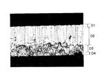
- FIG. 2 shows a cut surface (micrograph) of the metal plate punched out by the press. As shown in FIG.
- the cut surface of the metal plate punched out by press working has a sagging surface D1 having a smooth round shape in order from the upper surface side to the lower side, and has glossy and vertical stripes.
- a shearing surface D2 a fractured surface D3 from which a metal material has been peeled off, and a return surface D4 with burrs are formed.
- the shear surface indicated by D2 in FIG. 2 has the largest unevenness of the height difference and protrudes highest from the surface. 2 is upside down with respect to FIG. 1 and FIG.
- FIGS. 3A When the press die 14 is lowered, the lower surface of the press die 14 contacts the metal plate 11 and pushes the metal plate 11 downward.
- sagging (D 1) is generated on the blade surface side of the press die 14 and the blade side surface side of the die 12 in the metal plate 11.
- the press die 14 is further lowered, the metal plate 11 is subjected to a shear stress by the press die 14 and the die 12, and a shear surface (D2) is generated following the sag (D1).
- Fatigue failure has several factors, but when a plate such as a contact is subjected to repeated loads, the maximum stress is generated on the surface of the plate, and the stress concentration in the recess due to the surface roughness causes fatigue failure. One of the main factors.
- the contacts are also downsized. Therefore, the dimensional ratio of the unevenness with respect to the component cross-sectional area of the maximum stress portion in the contact also increases, and the contact easily breaks.
- the present invention has been made in view of the above technical problems, and an object of the present invention is to provide a contact having a high durability and a low cost, and a manufacturing method thereof.
- the contact according to the present invention is characterized in that the plate width is 0.1 mm or more and 1 mm or less, and the surface roughness Ra at the stress concentration location is 0.2 ⁇ m or less. According to such a contact, since the surface roughness Ra is 0.2 ⁇ m or less, the contact is less likely to break due to stress concentration, and the battery connector can be operated more than 3,000 times. Further, if the plate width is 0.1 mm or more and 1 mm or less, the durability is almost the same and the quality can be stabilized.
- An embodiment of the contact according to the present invention is characterized in that the surface roughness Ra is 0.08 ⁇ m or less. With such a surface roughness Ra, the battery connector can be operated more than 6,000 times.
- Another embodiment of the contact according to the present invention is characterized in that the surface roughness Ra is 0.04 ⁇ m or more. This is because if the surface roughness Ra is smaller than 0.04 ⁇ m by etching or polishing, the plate width and plate thickness necessary for maintaining the function as a contact are reduced.
- a first method for manufacturing a contact according to the present invention is a method for manufacturing a contact according to the present invention, in which a contact is manufactured by stamping with a press, and a surface of the contact manufactured by the above-described process is subjected to surface roughening. And a step of etching or polishing so that Ra is 0.2 ⁇ m or less. According to this manufacturing method, since the contact is manufactured by punching and etching (chemical polishing) or polishing (buff polishing, electrolytic polishing, etc.), a highly durable contact can be manufactured at low cost.
- a contact manufacturing method is a contact manufacturing method according to the present invention, comprising: forming a resist film on an electrode plate; and exposing and developing the resist film to form a cavity.
- the surface roughness Ra can be easily reduced by etching (chemical polishing) or polishing (buff polishing, electrolytic polishing, etc.).
- a third method for manufacturing a contact according to the present invention is a method for manufacturing a contact according to the present invention, comprising a step of adhering a dry film resist on an electrode plate and attaching the dry film resist to the surface of the dry film resist.
- a fourth method for manufacturing a contact according to the present invention is a method for manufacturing a contact according to the present invention, wherein a resist film is formed by applying a resist solution on an electrode plate, and the resist film is formed by a LIGA process. And a step of forming a contact by electroforming in the cavity.
- a resist film is formed by applying a resist solution on an electrode plate, and the resist film is formed by a LIGA process.
- a step of forming a contact by electroforming in the cavity According to the LIGA process, since the wall surface of the cavity can be formed smoothly, a contact having a small surface roughness Ra can be manufactured without performing etching or polishing in a subsequent process.
- a fifth method for manufacturing a contact according to the present invention is a method for manufacturing a contact according to the present invention, comprising: applying a resist solution on an electrode plate to form a resist film; and performing the above-described process by a UV-LIGA process.
- the method includes a step of opening a cavity in the resist film, and a step of forming a contact in the cavity by electroforming. According to the UV-LIGA process, since the wall surface of the cavity can be formed smoothly, a contact having a small surface roughness Ra can be manufactured without performing etching or polishing in a subsequent process.
- a sixth method for manufacturing a contact according to the present invention is a method for manufacturing a contact according to the present invention, in which a dry film resist is adhered and adhered on an electrode plate, and a protective film on the surface is removed to form a photosensitive layer. It is characterized by comprising a step of exposing, a step of exposing and developing the photosensitive layer in a non-oxygen atmosphere to open a cavity, and a step of forming a contact in the cavity by electroforming. Since the wall surface of the cavity can be formed smoothly if the dry film resist is adhered and adhered, and the protective film on the surface is removed and exposed, the surface roughness Ra can be reduced without performing etching or polishing in the subsequent process. Small contacts can be manufactured. However, if the protective film is removed, oxygen inhibition occurs depending on the photosensitive layer, and exposure development is performed in a non-oxygen atmosphere to prevent this.
- a seventh method for manufacturing a contact according to the present invention is a method for manufacturing a contact according to the present invention, wherein the transparency, particle shape, or particle size of the protective film lubricant is adjusted on the electrode plate. And a step of exposing and developing the dry film resist to open a cavity, and a step of forming a contact in the cavity by electroforming. If the lubricant in the protective film is selected, the wall surface of the cavity can be formed smoothly, so that a contact having a small surface roughness Ra can be produced without performing etching or polishing in a subsequent process.
- the means for solving the above-described problems in the present invention has a feature in which the above-described constituent elements are appropriately combined, and the present invention enables many variations by combining such constituent elements. .
- FIG. 1A and FIG. 1B are schematic views for explaining a contact manufacturing method using a press.
- FIG. 2 shows a cross section of a metal part stamped out by a press.
- 3 (A) to 3 (D) are diagrams for explaining a mechanism in which a cut surface is generated in the metal plate.
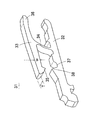
- FIG. 4 is a perspective view of the connector contact according to the first embodiment of the present invention.
- FIG. 5 is a cross-sectional view of a connector incorporating the contact of FIG.
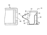
- FIG. 6 is a cross-sectional view of the battery connector.
- FIG. 7 is a diagram showing the relationship between the surface roughness Ra and the number of repeated fractures.
- FIG. 8 is a diagram illustrating the relationship between the contact plate width w and the number of repeated breaks.
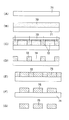
- FIGS. 9A to 9D are schematic diagrams for explaining a contact manufacturing method 1.
- FIGS. 10A to 10G are schematic diagrams for explaining a contact manufacturing method 4.
- FIG. 4 is a perspective view of the connector contact 31 (connector connection terminal).
- FIG. 5 is a cross-sectional view of a connector 41 incorporating this contact 31.
- the fixed piece 32 and the movable piece 33 are arranged substantially in parallel, and the upper surface of the substantially central portion of the fixed piece 32 and the lower surface of the substantially central portion of the movable piece 33 are arranged on both pieces 32 and 33. It is a shape connected by a vertical connecting portion 34.
- a movable contact 35 having a triangular protrusion shape is provided on the lower surface of the distal end portion of the movable piece 33, and the rear end portion of the movable piece 33 serves as an operation receiving portion 36 for tilting the movable piece 33 by the cam portion.
- a groove 37 and a retaining projection 38 are provided on the upper surface of the fixed piece 32 at a position facing the movable contact 35.
- the contact 31 is incorporated in the housing 42 of the connector 41 as shown in FIG.
- the contact 31 is fixed by press-fitting the fixing piece 32 into the insertion hole 43 of the housing 42.
- a cam portion 44 for pushing up the operation receiving portion 36 is located between the upper surface of the rear end portion of the fixed piece 32 and the lower surface of the operation receiving portion 36.
- the cam portion 44 is formed integrally with the operation lever 45, and the cam portion 44 rotates by raising or lowering the operation lever 45. In the state where the operation lever 45 is raised, the cam portion 44 falls to the side and does not exert a force on the operation receiving portion 36. Therefore, at this time, the gap between the movable contact 35 and the fixed piece 32 is wide, and the end portion of the flexible printed circuit board 46 can be inserted into and removed from the gap between the movable contact 35 and the fixed piece 32.
- the movable contact 35 is pressed against an electrode portion (not shown) of the flexible printed circuit board 46, and the flexible printed circuit board 46 is gripped while being bent between the movable contact 35, the groove portion 37, and the retaining projection 38. Is prevented from coming off.
- FIG. 6 is a cross-sectional view of the battery connector 51.
- the connector 51 has a plurality of contacts 53 housed in a connector housing 52, and a part of the contacts 53 protrudes from the front surface of the connector housing 52.
- the contact 53 includes a fixed portion 54, an elastic portion 55, a contact portion 56, and a latching portion 57.
- the fixing portion 54 of the contact 53 extends along the inner surface of the connector housing 52, and the lower end portion is fixed to the connector housing 52.
- the elastic part 55 of the contact 53 is substantially S-shaped, so that the contact 53 can generate a sufficient urging force in the front-rear direction.
- the contact portion 56 of the contact 53 is curved backward from the front end of the elastic portion 55 in a substantially U shape or arc shape.
- the latching portion 57 of the contact 53 is formed by folding back further downward from the end portion of the contact portion 56, and the latching portion 57 is latched on a contact support portion 58 provided in the opening of the connector housing 52. Has been.
- the connector 51 is in contact with a battery 59 for portable equipment. That is, when the battery 59 is pressed against the connector 51, the contact portion 56 comes into contact with the electrode portion 60 of the battery 59 and bends, and a charging current is supplied from the connector 51 to the battery 59.
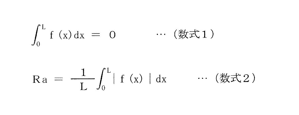
- the surface roughness (arithmetic average roughness) Ra is defined as follows.
- the y-axis is taken in the direction perpendicular to the surface (height direction)
- the x-axis is taken in the direction parallel to the surface
- the x-axis is determined so as to coincide with the average line.
- average roughness Ra is expressed the value calculated
- FIG. 7 shows the relationship between the surface roughness Ra obtained by experiments and the number of repeated fractures.
- a contact for a battery connector as shown in FIG. 6 having a plate thickness of 250 ⁇ m made of a Ni-based alloy was used.
- four types of samples having surface roughness Ra of 0.040 ⁇ m, 0.080 ⁇ m, 0.120 ⁇ m and 0.180 ⁇ m were produced.
- the contact thickness T is the thickness of the contact in the direction perpendicular to the surface when the contact is deformed (when the contact is stamped by a press). If so, the thickness of the metal plate as the material), and the plate width w is the width of the contact in the plane.
- the contact surface roughness Ra in order to satisfy the battery connector operation frequency of 3,000, the contact surface roughness Ra needs to be 0.2 ⁇ m or less. In addition, in order to satisfy the 6,000 times of repeated breaking, which is approximately twice the safety factor of the battery connector operation frequency, the contact surface roughness Ra should be 0.1 ⁇ m or less, preferably 0.08 ⁇ m or less. It is necessary to.
- the surface roughness Ra can be set to 0.04 ⁇ m or less by the method of reducing the unevenness of the contact surface by etching.
- FIG. 8 shows the relationship between the contact width w and the number of repeated breaks.
- a contact for a battery connector as shown in FIG. 6 having a plate thickness of 250 ⁇ m made of a Ni-based alloy was used.
- Samples having different plate widths w were produced one by one in the range of plate widths w of 0.1 to 1.0 mm.
- a load was applied so that the maximum stress was 1000 MPa (spring limit value), the contact was repeatedly elastically deformed, and the number of times until the contact was broken was measured.
- the individual data measured in this way are indicated by black circles in FIG. According to FIG. 8, there is no significant difference in the number of repeated fractures when the plate width w is in the range of 0.1 mm to 1 mm.
- the contact in order to achieve the required number of repeated fractures, preferably has a plate width of 0.1 mm or more and 1 mm or less, and its surface roughness (particularly, surface roughness at the stress concentration location) Ra Is preferably 0.04 ⁇ m or more and 0.2 ⁇ m or less, and particularly preferably the surface roughness Ra is 0.04 ⁇ m or more and 0.080 ⁇ m or less.
- FIGS. 9A to 9D The method shown in FIGS. 9A to 9D is a method using a press. That is, FIG. 9A shows a metal plate 61 having a plate thickness T of about 100 ⁇ m. The metal plate 61 is punched into a contact shape as shown in FIG. When the surface roughness Ra of the contact at this stage was measured, the surface roughness Ra of the shearing surface of phosphor bronze was 0.23 ⁇ m. Next, the surface of the contact 62 in FIG. 9C was etched, and the surface irregularities were removed and smoothed as shown in FIG. 9D. As the etching solution used at this time, for example, etching solution E-screen S-710 manufactured by Sasaki Chemical Co., Ltd. was used.
- etching solution E-screen S-710 manufactured by Sasaki Chemical Co., Ltd. was used.
- a contact 62 having a surface roughness Ra of 0.04 ⁇ m or less could be produced.
- the surface roughness Ra is set to 0.04 ⁇ m or less, the plate thickness and the plate width of the contact 62 are considerably reduced. Therefore, it is necessary to set the dimensions to allow for the reduction when punching with a press.
- the surface of the contact 62 may be polished so that the surface roughness Ra falls within a predetermined range.
- electrolytic polishing or buffing can be used as a polishing method.
- the surface of the contact 62 may be coated with metal.
- a metal material can be plated on the surface of the contact 62 or vacuum deposited.
- the coated metal is buried in the recess, so that the surface roughness Ra is reduced.
- FIGS. 10A to 10G show a method using photolithography and electroforming.
- a negative resist is applied to the upper surface of the electrode plate 71 as shown in FIG. 10A, and a resist film 72 is formed as shown in FIG.
- a photomask 73 is superimposed on the resist film 72 and exposed, and then developed as shown in FIG. 10D. Since the exposed area is insolubilized, the resist film 72 in the area that is covered with the mask and is not exposed is removed, and a contact-shaped cavity 74 is formed at the trace. Thereafter, as shown in FIG.
- a metal material is deposited in the cavity 74 using the electrode plate 71 as an electrode, and the contact 75 is formed in the cavity 74.
- the contact 75 is released from the electrode plate 71 as shown in FIG. 10 (G). According to such a method, a contact having a surface roughness Ra of 0.2 ⁇ m or less or 0.080 ⁇ m or less can be directly produced without requiring post-treatment.
- the method can be further divided into several methods.
- the first is a method of patterning a resist film by a UV-LIGA process using a thick film resist such as Su-8 manufactured by Kayaku Microchem Corporation as a resist. According to this method, a smooth contact having no irregularities on the outer peripheral surface can be produced.
- the second method uses a dry film resist.
- a protective film is pasted on the surface of the photosensitive layer. Since this protective film contains a lubricant, when exposed while the protective film is stuck, a streak is formed on the wall surface of the cavity due to the lubricant, and this is transferred to the contact. Therefore, when a dry film resist is used, if the protective film is peeled off and only the photosensitive layer is used as the resist film, a contact with a smooth outer peripheral surface that does not have a streak on the outer peripheral surface can be manufactured.
- the photosensitive layer of the dry film resist has a characteristic of causing oxygen inhibition
- the protective film may be peeled off from the photosensitive layer, and the exposure may be performed in an oxygen-free environment such as N 2 atmosphere or in a vacuum atmosphere.
- the third method is a method using a LIGA process.
- PMMA polymethyl methacrylate
- SR light X-rays are irradiated instead of ultraviolet irradiation, and the pattern of the X-ray absorber on the photomask is transferred to the resist film. By doing so, create metal parts that are not uneven on the wall.
- the dry film resist is rolled up in the manufacturing process, particles called a lubricant are mixed in the protective film for the purpose of improving the slipping property.
- the photosensitive layer of the dry film resist has oxygen inhibition characteristics, so that exposure is performed while leaving the protective film so as not to touch oxygen.
- the lubricant causes light scattering, and the light intensity distribution is changed to generate vertical stripes at the boundary between the hardened portion and the uncured portion of the resist film.
- the surface roughness Ra of the outer peripheral surface of the contact 75 at the stage of FIG. Therefore, in the manufacturing method 5, the contact 75 is etched in the next step of FIG.
- the etching solution for example, the etching solution E-screen MY-28 manufactured by Sasaki Chemical Co., Ltd. can be used, and the surface roughness Ra of the contact can be reduced to 0.04 ⁇ m or less.
- the surface roughness Ra may be reduced by performing electropolishing or buffing without using etching (chemical polishing).
Landscapes
- Engineering & Computer Science (AREA)
- Manufacturing & Machinery (AREA)
- Manufacturing Of Electrical Connectors (AREA)
- Connection Of Batteries Or Terminals (AREA)
- Coupling Device And Connection With Printed Circuit (AREA)
Abstract
Description
また、板幅が0.1mm以上1mm以下であれば、耐久性がほぼ同等で品質を安定させることができる。
図4及び図5を参照してコネクタ用のコンタクトを説明する。図4は、コネクタ用のコンタクト31(コネクタ用接続端子)の斜視図である。図5は、このコンタクト31を組み込んだコネクタ41の断面図である。
つぎに、たとえば携帯用電子機器に使用されるバッテリーの電極パッドに接触させて充電を行わせるためのコネクタについて説明する。図6は、バッテリーコネクタ51の断面図である。
このようなバッテリーコネクタ用のコンタクトを一例として、その表面粗さRa(両側面と垂直な外周面における表面粗さRa)と繰返し破断回数との関係について調べた。ここで、表面粗さ(算術平均粗さ)Raとは、つぎのように定義される。ある断面の表面形状を考えるとき、その表面に垂直な方向(高さ方向)にy軸をとり、表面に平行な方向にx軸をとり、その表面形状を粗さ曲線y=f(x)で表わす。ただし、x軸は平均線と一致するように定める。すなわち、高さ方向の原点(y=0の位置)は、表面粗さを考える領域(x=0からx=Lまで)において、下記数式1を満たすように定める。そして、当該領域[0、L]において下記数式2によって求められる値をμm単位で表したものを平均粗さRaという。
板幅wが0.1-1.0mmの範囲で、板幅wの異なるサンプルを1個ずつ作製した。各サンプルの表面粗さは、その影響が顕著に表れるようにRa=0.18μmとした。そして、最大応力が1000MPa(ばね限界値)となるように負荷を加えてコンタクトを繰り返し弾性変形させ、コンタクトが破断に至るまでの回数を測定した。こうして測定した個々のデータを図8に黒丸で示す。図8によれば、板幅wが0.1mm以上1mmの範囲で繰返し破断回数に有意差は見られない。
上記のような板幅と表面粗さRaを有するコンタクトを作製する方法としては、種々の方法があるので、これらを説明する。
図9(A)-図9(D)に示すものは、プレスによる方法である。すなわち、図9(A)は、板厚Tが100μm程度の金属板61を示す。この金属板61を、図9(B)に示すようにコンタクト形状に打ち抜いてコンタクト62を得る。この段階でのコンタクトの表面粗さRaを実測したところ、リン青銅での剪断面の表面粗さRaは0.23μmであった。ついで、図9(C)のコンタクト62の表面をエッチング処理し、図9(D)のように表面の凹凸を除去して平滑化させた。この際に用いたエッチング液は、たとえば佐々木化学薬品株式会社製のエッチング液エスクリーンS-710等を使用した。その結果、表面粗さRaが0.04μm以下のコンタクト62を作製することができた。ただし、表面粗さRaを0.04μm以下にすると、コンタクト62の板厚や板幅もかなり減少するので、プレスによる打ち抜き時に減少分を見込んだ寸法にしておく必要がある。
図9(A)-図9(C)のように金属板61からコンタクト62を打ち抜いた後、コンタクト62の表面を研磨して表面粗さRaを所定範囲に納めるようにしてもよい。研磨方法としては、電解研磨やバフ研磨を用いることができる。
図9(A)-図9(C)のように金属板61からコンタクト62を打ち抜いた後、コンタクト62の表面を金属で被覆処理してもよい。たとえば、金属材料をコンタクト62の表面にメッキしたり、真空蒸着したりすることができる。表面粗さRaの大きなコンタクト62に金属で被覆処理すると、被覆金属が凹部内に埋まるので、表面粗さRaが小さくなる。
図10(A)-図10(G)は、フォトリソグラフィと電鋳法を用いる方法である。まず、図10(A)のような電極板71の上面にネガレジストを塗布し、図10(B)のようにレジスト膜72を成膜する。図10(C)に示すように、レジスト膜72の上にフォトマスク73を重ねて露光し、ついで図10(D)に示すように現像する。露光領域は不溶化するので、マスクで覆われていて露光しなかった領域のレジスト膜72は除去され、その跡にコンタクト形状のキャビティ74ができる。この後、図10(E)に示すように、電極板71を電極としてキャビティ74内に金属材料を析出させ、キャビティ74内にコンタクト75を成形する。図10(F)のように電極板71の上のレジスト膜72を除去した後、図10(G)のように電極板71からコンタクト75を離型する。このような方法によれば、後処理を必要とせず、直接的に表面粗さRaが0.2μm以下や0.080μm以下のコンタクトを作製することができる。
この製造方法では、図10(B)の工程において電極板71の上にドライフィルムレジストを貼ってレジスト膜72を形成する。このときドライフィルムレジストの保護フィルムを剥がさないで、感光層(レジスト膜)の上に保護フィルムを残しておく。ついで、製造方法4と同様に図10(C)-図10(G)のフォトリソグラフィや電鋳の工程などを経てコンタクト75を製造する。
32 固定片
33 可動片
34 連結部
35 可動接点
41 コネクタ
42 ハウジング
51 コネクタ
52 コネクタハウジング
53 コンタクト
59 バッテリー
61 金属板
71 電極板
72 レジスト膜
73 フォトマスク
74 キャビティ
Claims (9)
- 板幅が0.1mm以上1mm以下で、かつ、応力集中箇所における表面粗さRaが0.2μm以下であることを特徴とするコンタクト。
- 表面粗さRaが0.08μm以下であることを特徴とする、請求項1に記載のコンタクト。
- 表面粗さRaが0.04μm以上であることを特徴とする、請求項1に記載のコンタクト。
- 請求項1に記載したコンタクトの製造方法であって、
プレスによる打ち抜き加工によりコンタクトを製造する工程と、
前記工程により作製されたコンタクトの表面を、表面粗さRaが0.2μm以下となるようにエッチング又は研磨する工程と、
を備えたコンタクトの製造方法。 - 請求項1に記載したコンタクトの製造方法であって、
電極板の上にレジスト膜を形成する工程と、
前記レジスト膜に露光及び現像を施してキャビティを開口する工程と、
前記キャビティ内に電鋳法によってコンタクトを成形する工程と、
前記レジスト膜と分離したコンタクトの表面を、表面粗さRaが0.2μm以下となるようにエッチング又は研磨する工程と、
を備えたコンタクトの製造方法。 - 請求項1に記載したコンタクトの製造方法であって、
電極板の上にドライフィルムレジストを密着させて貼り付ける工程と、
前記ドライフィルムレジストの表面に保護フィルムを残したままで前記ドライフィルムレジストに露光及び現像を施してキャビティを開口する工程と、
前記キャビティ内に電鋳法によってコンタクトを成形する工程と、
前記ドライフィルムレジストと分離したコンタクトの表面を、表面粗さRaが0.2μm以下となるようにエッチング又は研磨する工程と、
を備えたコンタクトの製造方法。 - 請求項1に記載したコンタクトの製造方法であって、
電極板の上にレジスト液を塗布してレジスト膜を形成する工程と、
LIGAプロセスによって前記レジスト膜にキャビティを開口する工程と、
前記キャビティ内に電鋳法によってコンタクトを成形する工程と、
を備えたコンタクトの製造方法。 - 請求項1に記載したコンタクトの製造方法であって、
電極板の上にレジスト液を塗布してレジスト膜を形成する工程と、
UV-LIGAプロセスによって前記レジスト膜にキャビティを開口する工程と、
前記キャビティ内に電鋳法によってコンタクトを成形する工程と、
を備えたコンタクトの製造方法。 - 請求項1に記載したコンタクトの製造方法であって、
電極板の上にドライフィルムレジストを密着させて貼り付け、表面の保護フィルムを取り除いて感光層を露出させる工程と、
非酸素雰囲気中において前記感光層に露光及び現像を施してキャビティを開口する工程と、
前記キャビティ内に電鋳法によってコンタクトを成形する工程と、
を備えたコンタクトの製造方法。
Priority Applications (3)
| Application Number | Priority Date | Filing Date | Title |
|---|---|---|---|
| US13/264,769 US8696392B2 (en) | 2011-03-15 | 2011-03-24 | Contact and method for manufacturing the contact |
| CN201180001907.4A CN102792525B (zh) | 2011-03-15 | 2011-03-24 | 接触件及其制造方法 |
| KR1020117024788A KR101131299B1 (ko) | 2011-03-15 | 2011-03-24 | 콘택트 및 그 제조 방법 |
Applications Claiming Priority (2)
| Application Number | Priority Date | Filing Date | Title |
|---|---|---|---|
| JP2011057075A JP4803329B1 (ja) | 2011-03-15 | 2011-03-15 | コンタクト及びその製造方法 |
| JP2011-057075 | 2011-03-15 |
Publications (1)
| Publication Number | Publication Date |
|---|---|
| WO2012124168A1 true WO2012124168A1 (ja) | 2012-09-20 |
Family
ID=44946851
Family Applications (1)
| Application Number | Title | Priority Date | Filing Date |
|---|---|---|---|
| PCT/JP2011/057162 Ceased WO2012124168A1 (ja) | 2011-03-15 | 2011-03-24 | コンタクト及びその製造方法 |
Country Status (4)
| Country | Link |
|---|---|
| JP (1) | JP4803329B1 (ja) |
| CN (1) | CN102792525B (ja) |
| TW (1) | TWI459667B (ja) |
| WO (1) | WO2012124168A1 (ja) |
Cited By (2)
| Publication number | Priority date | Publication date | Assignee | Title |
|---|---|---|---|---|
| WO2014187727A1 (de) * | 2013-05-24 | 2014-11-27 | Continental Teves Ag & Co. Ohg | Verfahren zur fertigung eines kontaktelements, kontaktelement sowie dessen verwendung |
| JP2020187840A (ja) * | 2019-05-10 | 2020-11-19 | イリソ電子工業株式会社 | 端子及びコネクタ |
Families Citing this family (3)
| Publication number | Priority date | Publication date | Assignee | Title |
|---|---|---|---|---|
| DE102012024185A1 (de) | 2012-12-11 | 2014-06-12 | Rosenberger Hochfrequenztechnik Gmbh & Co. Kg | Kontaktelement und Verfahren zu seiner Herstellung |
| US9142903B2 (en) * | 2013-11-22 | 2015-09-22 | Tektronix, Inc. | High performance multiport connector system using LIGA springs |
| US9568499B2 (en) * | 2013-11-22 | 2017-02-14 | Tektronix, Inc. | High performance LIGA spring interconnect system for probing application |
Citations (5)
| Publication number | Priority date | Publication date | Assignee | Title |
|---|---|---|---|---|
| JPS55144617A (en) * | 1979-04-28 | 1980-11-11 | Anritsu Electric Co Ltd | Electric contactor honing machine |
| JPH0482176A (ja) * | 1990-07-24 | 1992-03-16 | Yamaichi Electron Co Ltd | ソケットにおける電気接触子の冷却構造 |
| JPH0424826B2 (ja) * | 1983-06-30 | 1992-04-28 | Duracell Int | |
| JPH10199651A (ja) * | 1997-01-07 | 1998-07-31 | Yuken Kogyo Kk | 信号用コネクタの製造方法 |
| JP2003045539A (ja) * | 2001-05-22 | 2003-02-14 | Enplas Corp | コンタクトピン及び電気部品用ソケット |
Family Cites Families (2)
| Publication number | Priority date | Publication date | Assignee | Title |
|---|---|---|---|---|
| US6439975B1 (en) * | 2000-01-28 | 2002-08-27 | Hon Hai Precision Ind. Co., Ltd. | Method for forming contact of electrical connector and press die for practicing the method |
| JP5174582B2 (ja) * | 2007-08-30 | 2013-04-03 | 日本碍子株式会社 | 接合構造体 |
-
2011
- 2011-03-15 JP JP2011057075A patent/JP4803329B1/ja active Active
- 2011-03-24 CN CN201180001907.4A patent/CN102792525B/zh not_active Expired - Fee Related
- 2011-03-24 WO PCT/JP2011/057162 patent/WO2012124168A1/ja not_active Ceased
- 2011-10-11 TW TW100136639A patent/TWI459667B/zh not_active IP Right Cessation
Patent Citations (5)
| Publication number | Priority date | Publication date | Assignee | Title |
|---|---|---|---|---|
| JPS55144617A (en) * | 1979-04-28 | 1980-11-11 | Anritsu Electric Co Ltd | Electric contactor honing machine |
| JPH0424826B2 (ja) * | 1983-06-30 | 1992-04-28 | Duracell Int | |
| JPH0482176A (ja) * | 1990-07-24 | 1992-03-16 | Yamaichi Electron Co Ltd | ソケットにおける電気接触子の冷却構造 |
| JPH10199651A (ja) * | 1997-01-07 | 1998-07-31 | Yuken Kogyo Kk | 信号用コネクタの製造方法 |
| JP2003045539A (ja) * | 2001-05-22 | 2003-02-14 | Enplas Corp | コンタクトピン及び電気部品用ソケット |
Cited By (3)
| Publication number | Priority date | Publication date | Assignee | Title |
|---|---|---|---|---|
| WO2014187727A1 (de) * | 2013-05-24 | 2014-11-27 | Continental Teves Ag & Co. Ohg | Verfahren zur fertigung eines kontaktelements, kontaktelement sowie dessen verwendung |
| JP2020187840A (ja) * | 2019-05-10 | 2020-11-19 | イリソ電子工業株式会社 | 端子及びコネクタ |
| JP7493308B2 (ja) | 2019-05-10 | 2024-05-31 | イリソ電子工業株式会社 | 端子及びコネクタと端子の製造方法 |
Also Published As
| Publication number | Publication date |
|---|---|
| CN102792525A (zh) | 2012-11-21 |
| JP2012195110A (ja) | 2012-10-11 |
| CN102792525B (zh) | 2015-01-28 |
| JP4803329B1 (ja) | 2011-10-26 |
| TW201238187A (en) | 2012-09-16 |
| TWI459667B (zh) | 2014-11-01 |
Similar Documents
| Publication | Publication Date | Title |
|---|---|---|
| JP4803329B1 (ja) | コンタクト及びその製造方法 | |
| US8696392B2 (en) | Contact and method for manufacturing the contact | |
| JP2009527759A (ja) | プローブピン組立体及びその製造方法 | |
| JP2009128218A (ja) | 電気接触子およびそれを備える検査冶具 | |
| JP2009021238A (ja) | コンプライアントピン | |
| US8678851B2 (en) | Contact section having an irregular shape formed thereon by electroforming | |
| CN108140972B (zh) | 连接器端子及其制造方法 | |
| JP5615740B2 (ja) | 異方導電性シートおよび異方導電性シートの製造方法 | |
| CN101471505B (zh) | 连接器用连接端子 | |
| CN1630455A (zh) | 布线电路基板保持板及其制造方法 | |
| JP4337498B2 (ja) | 導電性ペーストの塗布方法および導電性ペーストの塗布装置 | |
| KR101131299B1 (ko) | 콘택트 및 그 제조 방법 | |
| KR20240025311A (ko) | 디스플레이 부품 검사 소켓용 지그 | |
| US20200321144A1 (en) | Electric connector and method for manufacturing the same | |
| KR20020089151A (ko) | 콘택트핀 및 전기부품용 소켓 | |
| JP2011150837A (ja) | 回路接続部材、導電性粒子および導電性粒子の製造方法 | |
| JP2003043064A (ja) | 接触子製造用金型及びその製造方法並びに接触子の製造方法 | |
| US6988310B2 (en) | Method of assembling an interconnect device assembly | |
| CN115696765A (zh) | 一种提高pcb焊盘精度及拉脱强度的制作方法 | |
| WO2013088753A1 (ja) | コンタクト及びその製造方法 | |
| CN1455259A (zh) | 生产探针的方法,生产探针的掩模,以及探针 | |
| JP4490338B2 (ja) | プローブユニットの製造方法及びそれを用いたプローブユニット | |
| KR0151002B1 (ko) | 리이드 프레임 제조방법 및 그 장치 | |
| CN118091211A (zh) | 接触探针及用于电气部件测试的插座 | |
| TW200500760A (en) | Method for manufacturing electronic device and electronic device |
Legal Events
| Date | Code | Title | Description |
|---|---|---|---|
| WWE | Wipo information: entry into national phase |
Ref document number: 201180001907.4 Country of ref document: CN |
|
| ENP | Entry into the national phase |
Ref document number: 20117024788 Country of ref document: KR Kind code of ref document: A |
|
| WWE | Wipo information: entry into national phase |
Ref document number: 13264769 Country of ref document: US |
|
| 121 | Ep: the epo has been informed by wipo that ep was designated in this application |
Ref document number: 11860739 Country of ref document: EP Kind code of ref document: A1 |
|
| NENP | Non-entry into the national phase |
Ref country code: DE |
|
| 122 | Ep: pct application non-entry in european phase |
Ref document number: 11860739 Country of ref document: EP Kind code of ref document: A1 |