WO2012121526A2 - 적외선 센서칩, 적외선 감지기, 이의 동작 방법 및 테스트 방법 - Google Patents
적외선 센서칩, 적외선 감지기, 이의 동작 방법 및 테스트 방법 Download PDFInfo
- Publication number
- WO2012121526A2 WO2012121526A2 PCT/KR2012/001612 KR2012001612W WO2012121526A2 WO 2012121526 A2 WO2012121526 A2 WO 2012121526A2 KR 2012001612 W KR2012001612 W KR 2012001612W WO 2012121526 A2 WO2012121526 A2 WO 2012121526A2
- Authority
- WO
- WIPO (PCT)
- Prior art keywords
- switch
- output multiplexer
- cell
- reference cell
- chip
- Prior art date
Links
- 238000010998 test method Methods 0.000 title claims description 4
- 238000011017 operating method Methods 0.000 title claims description 3
- 238000012360 testing method Methods 0.000 claims abstract description 26
- 239000011159 matrix material Substances 0.000 claims abstract description 9
- 238000000034 method Methods 0.000 claims description 16
- 238000012545 processing Methods 0.000 claims description 3
- 229920006395 saturated elastomer Polymers 0.000 claims description 2
- 238000010586 diagram Methods 0.000 description 28
- 238000004519 manufacturing process Methods 0.000 description 9
- 238000012544 monitoring process Methods 0.000 description 5
- 238000013475 authorization Methods 0.000 description 4
- 238000004806 packaging method and process Methods 0.000 description 3
- 239000000758 substrate Substances 0.000 description 3
- 230000002950 deficient Effects 0.000 description 2
- 238000011161 development Methods 0.000 description 2
- 238000011156 evaluation Methods 0.000 description 2
- 230000014509 gene expression Effects 0.000 description 2
- 230000004913 activation Effects 0.000 description 1
- 230000000903 blocking effect Effects 0.000 description 1
- 230000007547 defect Effects 0.000 description 1
- 238000013461 design Methods 0.000 description 1
- 238000013100 final test Methods 0.000 description 1
- 238000005259 measurement Methods 0.000 description 1
- 238000000926 separation method Methods 0.000 description 1
Images


Classifications
-
- G—PHYSICS
- G01—MEASURING; TESTING
- G01J—MEASUREMENT OF INTENSITY, VELOCITY, SPECTRAL CONTENT, POLARISATION, PHASE OR PULSE CHARACTERISTICS OF INFRARED, VISIBLE OR ULTRAVIOLET LIGHT; COLORIMETRY; RADIATION PYROMETRY
- G01J5/00—Radiation pyrometry, e.g. infrared or optical thermometry
- G01J5/02—Constructional details
- G01J5/026—Control of working procedures of a pyrometer, other than calibration; Bandwidth calculation; Gain control
-
- G—PHYSICS
- G01—MEASURING; TESTING
- G01J—MEASUREMENT OF INTENSITY, VELOCITY, SPECTRAL CONTENT, POLARISATION, PHASE OR PULSE CHARACTERISTICS OF INFRARED, VISIBLE OR ULTRAVIOLET LIGHT; COLORIMETRY; RADIATION PYROMETRY
- G01J5/00—Radiation pyrometry, e.g. infrared or optical thermometry
- G01J5/10—Radiation pyrometry, e.g. infrared or optical thermometry using electric radiation detectors
- G01J5/20—Radiation pyrometry, e.g. infrared or optical thermometry using electric radiation detectors using resistors, thermistors or semiconductors sensitive to radiation, e.g. photoconductive devices
- G01J5/22—Electrical features thereof
- G01J5/24—Use of specially adapted circuits, e.g. bridge circuits
-
- H—ELECTRICITY
- H01—ELECTRIC ELEMENTS
- H01L—SEMICONDUCTOR DEVICES NOT COVERED BY CLASS H10
- H01L2224/00—Indexing scheme for arrangements for connecting or disconnecting semiconductor or solid-state bodies and methods related thereto as covered by H01L24/00
- H01L2224/01—Means for bonding being attached to, or being formed on, the surface to be connected, e.g. chip-to-package, die-attach, "first-level" interconnects; Manufacturing methods related thereto
- H01L2224/42—Wire connectors; Manufacturing methods related thereto
- H01L2224/47—Structure, shape, material or disposition of the wire connectors after the connecting process
- H01L2224/48—Structure, shape, material or disposition of the wire connectors after the connecting process of an individual wire connector
- H01L2224/4805—Shape
- H01L2224/4809—Loop shape
- H01L2224/48091—Arched
-
- H—ELECTRICITY
- H01—ELECTRIC ELEMENTS
- H01L—SEMICONDUCTOR DEVICES NOT COVERED BY CLASS H10
- H01L2224/00—Indexing scheme for arrangements for connecting or disconnecting semiconductor or solid-state bodies and methods related thereto as covered by H01L24/00
- H01L2224/01—Means for bonding being attached to, or being formed on, the surface to be connected, e.g. chip-to-package, die-attach, "first-level" interconnects; Manufacturing methods related thereto
- H01L2224/42—Wire connectors; Manufacturing methods related thereto
- H01L2224/47—Structure, shape, material or disposition of the wire connectors after the connecting process
- H01L2224/48—Structure, shape, material or disposition of the wire connectors after the connecting process of an individual wire connector
- H01L2224/481—Disposition
- H01L2224/48135—Connecting between different semiconductor or solid-state bodies, i.e. chip-to-chip
- H01L2224/48137—Connecting between different semiconductor or solid-state bodies, i.e. chip-to-chip the bodies being arranged next to each other, e.g. on a common substrate
-
- H—ELECTRICITY
- H01—ELECTRIC ELEMENTS
- H01L—SEMICONDUCTOR DEVICES NOT COVERED BY CLASS H10
- H01L2224/00—Indexing scheme for arrangements for connecting or disconnecting semiconductor or solid-state bodies and methods related thereto as covered by H01L24/00
- H01L2224/01—Means for bonding being attached to, or being formed on, the surface to be connected, e.g. chip-to-package, die-attach, "first-level" interconnects; Manufacturing methods related thereto
- H01L2224/42—Wire connectors; Manufacturing methods related thereto
- H01L2224/47—Structure, shape, material or disposition of the wire connectors after the connecting process
- H01L2224/49—Structure, shape, material or disposition of the wire connectors after the connecting process of a plurality of wire connectors
- H01L2224/491—Disposition
- H01L2224/4912—Layout
- H01L2224/49175—Parallel arrangements
-
- H—ELECTRICITY
- H01—ELECTRIC ELEMENTS
- H01L—SEMICONDUCTOR DEVICES NOT COVERED BY CLASS H10
- H01L2924/00—Indexing scheme for arrangements or methods for connecting or disconnecting semiconductor or solid-state bodies as covered by H01L24/00
- H01L2924/10—Details of semiconductor or other solid state devices to be connected
- H01L2924/11—Device type
- H01L2924/13—Discrete devices, e.g. 3 terminal devices
- H01L2924/1304—Transistor
- H01L2924/1305—Bipolar Junction Transistor [BJT]
- H01L2924/13055—Insulated gate bipolar transistor [IGBT]
-
- H—ELECTRICITY
- H01—ELECTRIC ELEMENTS
- H01L—SEMICONDUCTOR DEVICES NOT COVERED BY CLASS H10
- H01L2924/00—Indexing scheme for arrangements or methods for connecting or disconnecting semiconductor or solid-state bodies as covered by H01L24/00
- H01L2924/10—Details of semiconductor or other solid state devices to be connected
- H01L2924/146—Mixed devices
- H01L2924/1461—MEMS
-
- H—ELECTRICITY
- H01—ELECTRIC ELEMENTS
- H01L—SEMICONDUCTOR DEVICES NOT COVERED BY CLASS H10
- H01L2924/00—Indexing scheme for arrangements or methods for connecting or disconnecting semiconductor or solid-state bodies as covered by H01L24/00
- H01L2924/30—Technical effects
- H01L2924/301—Electrical effects
- H01L2924/3011—Impedance
Definitions
- the present invention relates to an infrared sensor chip, an infrared detector, a method of operation thereof and a test method thereof.
- the bolometer-type infrared detector has a resistance characteristic that varies with temperature.
- the infrared detector is composed of a sensor (e.g., a bolometer) and an output control integrated circuit (ROIC) for processing a signal according to the amount of infrared light detected by the sensor. .
- a sensor e.g., a bolometer
- ROIC output control integrated circuit
- the output control integrated circuit (ROIC) is designed on the wafer in advance, and since the sensor is fabricated on the output control integrated circuit, there is a disadvantage that it is not easy to check the operation state of the sensor in advance.
- the present invention has been proposed to overcome the shortcomings according to the prior art raised above, to eliminate interference between the bolometer and the ROIC chip, and to enable testing at the wafer or chip level.
- an object of the present invention is to reduce the manufacturing cost of the infrared sensor, and to check the operation state of the sensor and / or the output control integrated circuit in advance to minimize the improvement of the yield through the process monitoring and the cost of the failure.
- a CMOS circuit board comprising an active matrix, a row line selector and an output multiplexer; And a bolometer stacked on the CMOS circuit board, the bolometer comprising an active cell and a reference cell, wherein the row line selector is a target of voltage application among the bolometers for a parametric test of the bolometer in a wafer or chip state.
- the cell multiplexer is selected, and the output multiplexer unit provides an infrared sensor chip for outputting a current characteristic according to the voltage application.
- a first switch for selectively connecting one input terminal of the reference cell and the output multiplexer unit and a second switch for selectively connecting the one input terminal of the active cell and the output multiplexer unit may be turned on / off by a control signal, respectively.
- a current value flowing through either the reference cell or the active cell may be output through the output multiplexer.
- a first switch for selectively connecting one input terminal of the reference cell and the output multiplexer unit and a second switch for selectively connecting the one input terminal of the active cell and the output multiplexer unit are controlled by an independent analog control signal so as to be saturated.
- the difference between the current flowing in the reference cell and the active cell may be amplified as it is or through an amplifier and input to the input terminal of the output multiplexer unit.
- a parametric test method of an infrared sensor including an active cell and a reference cell, the first switch selectively connecting one input terminal of the reference cell and an output multiplexer part, and one of the active cell and the output multiplexer part Sequentially turning on / off a second switch for selectively connecting an input terminal to sequentially receive values of current flowing through the reference cell and the active cell; And measuring resistance values of the reference cell and the active cell based on the value of the current, the voltage across the reference cell and the active cell.
- Independent variable analog power control signals for the on / off may be input to the first switch and the second switch, respectively.
- an operating method of an infrared sensor including an active cell and a reference cell, the method comprising applying an independent variable analog power control signal to a first switch for selectively connecting one input terminal of the reference cell and the output multiplexer unit; Applying an independent variable analog power control signal to a second switch for selectively connecting said active cell and said input terminal of said output multiplexer unit; And outputting the difference between the current flowing through the reference cell and the current flowing through the active cell as it is or amplifying the difference, and outputting the result to the outside through the output multiplexer.
- a circuit board including a row line selector and an output multiplexer, stacked on the circuit board, and selected by a signal from the row line selector to receive a current signal related to infrared sensing.
- An infrared sensor chip including an infrared sensor including a plurality of cells output to an output multiplexer; And a Sa-FPA controller chip electrically connected to the infrared sensor chip to apply a signal to control the row line selector and the output multiplexer, and to read the current signal transmitted from the output multiplexer.
- the Sa-FPA controller chip may be integrated with an ISP (Image Signal Processing) chip.
- ISP Image Signal Processing
- the Sa-FPA controller chip may be integrated with a DAC variable analog power chip.
- the present invention by separately manufacturing the infrared sensor chip except for the Sa-FPA controller chip, it is possible to test the bolometer at the wafer or chip stage, and thus, the cost generation due to the defect can be minimized.
- the manufacturing cost of the infrared detector can be lowered, the development period can be shortened, and the yield through process monitoring can be improved.
- FIG. 1 is a conceptual diagram schematically illustrating a configuration of an infrared detector using Sa-FPA according to an embodiment of the present invention.
- FIG. 2 is a flowchart illustrating a manufacturing process of an infrared sensor using Sa-FPA according to an embodiment of the present invention.
- 3 and 4 are block diagrams sequentially illustrating a manufacturing process of an infrared sensor using Sa-FPA according to the flowchart of FIG. 2.
- FIG. 5 is a circuit diagram showing the configuration of an infrared detector according to an embodiment of the present invention.
- FIG. 6 is a circuit diagram of a row control shift register in the circuit diagram shown in FIG.
- FIG. 7 is a circuit diagram of a column control shift register in the circuit diagram shown in FIG. 5.
- FIG 8 is another circuit diagram of an infrared sensor chip according to an embodiment of the present invention.
- FIG. 9 is a block diagram illustrating an operation mode and a test mode of an infrared sensor chip according to an exemplary embodiment of the present invention.
- 10 and 11 are circuit diagrams illustrating a configuration of an infrared sensor and an output multiplexer in the block diagram of FIG. 9.
- FIG. 12 is a circuit diagram illustrating a signal flow when the circuit diagram of FIG. 10 is in an operation mode.
- first and second may be used to describe various components, but the components should not be limited by the terms. The terms are used only for the purpose of distinguishing one component from another.
- first component may be referred to as the second component, and similarly, the second component may also be referred to as the first component.
- the term “and / or” includes any combination of a plurality of related items or any item of a plurality of related items.
- FIG. 1 is a conceptual diagram schematically showing the overall configuration of an infrared detector using Sa-FPA according to an embodiment of the present invention together with the overall configuration of a conventional infrared detector.
- an infrared detector according to an embodiment of the present invention is connected to an infrared sensor chip 100 and an infrared sensor chip 100 including a bolometer 120 formed on a basic logic / switch circuit board 110.
- Possible Sa-FPA controller chips 200 are included.
- the basic logic / switch circuit board 110 of the infrared sensor chip 100 includes an active matrix 111.
- it may include a row line selector and an output multiplexer for selecting each cell of the bolometer 120 formed on the active matrix and detecting a signal output from the cell.
- the low line selector applies power (for example, a voltage, etc.) to each cell of the bolometer 120, and the output multiplexer unit receives a response (for example, current characteristics, etc.) according to the power application, Print this out.
- the detailed configuration of the bolometer 120, the row line selector and the output multiplexer formed on the active matrix will be described later.
- the essential circuits for the cell selection of the active matrix and the bolometer 120 are formed on the basic logic / switch circuit board 110 of the infrared sensor chip 100. That is, the SA (Sense Amplifier) and the ADC (Analog to digital Converter), which were included in the ROIC on the conventional infrared sensor chip 100, are separated from the infrared sensor chip 100 and formed as a separate Sa-FPA controller chip 200. .
- SA Sense Amplifier
- ADC Analog to digital Converter
- the basic logic / switch circuit board 110 can be implemented as an inexpensive CMOS wafer having only a digital logic circuit having only an active matrix function, thereby significantly reducing manufacturing costs.
- electrical evaluation of each cell of the bolometer 120 may be performed at the wafer stage. Briefly describing this evaluation method, a parametric test is possible in a wafer or chip state by applying a voltage to each bolometer 120 and measuring a current characteristic. This will be described later in detail.
- the bolometer 120 may be stacked on the basic logic / switch circuit board 110 through a microelectromechanical systems (MEMS) process or the like, and may be monolithically stacked.
- MEMS microelectromechanical systems
- FIG. 2 is a flowchart illustrating a manufacturing process of an infrared sensor using Sa-FPA according to an embodiment of the present invention.
- a basic logic / switching device is designed in advance on a wafer (not shown) to prepare and prepare a basic logic / switch circuit board 110 (step S200).
- 3 is a diagram schematically illustrating a configuration of the basic logic / switch circuit board 110.
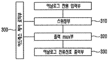
- FIG. 3 illustrates a basic logic / switch element substrate 110 including a variable analog power input unit such as an external D / A converter, a switching unit 310 connected to the analog power input unit and configured with a switching element.
- An output multiplexer unit 320 that is connected to the switching unit 310 and selects some of a plurality of current signals generated from the later-deposited bolometer, and transmits the current signal to the outside of the chip through the output multiplexer unit 320.
- the analog current signal output unit 330 and the address control logic unit 300 for controlling the switching unit 310 are designed and formed.
- the address control logic unit 300 may function as the row line selector and the output multiplexer.
- the switching unit 310 may be implemented as a switching device such as an NMOS transistor, a PMOS transistor, a CMOS transistor, and the like.
- the address control logic unit 300 may be implemented as a shift register for sequentially applying an address to the switching unit 310, a multiplexer for applying a random address, or the like.
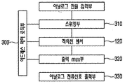
- the bolometer 120 is stacked on the basic logic / switch circuit board 110 using a monolithic method (step S210). A diagram showing this is shown in FIG. 4.
- the bolometer 120 is connected to the switching unit 310, which is also connected to the output multerplexer unit 320. In this way, the infrared sensor chip 100 is manufactured.
- the portion where the bolometer 120 is formed on the basic logic / switch circuit board 110 may be referred to as the active matrix described above.
- a parametric test is performed on the bolometer 120 in the wafer state (S220).
- a test may be performed at the wafer stage by applying a voltage to the active cell and the reference cell constituting the bolometer 120 and measuring current characteristics thereof. The test performed in step S220 will be described later in detail.
- step S250 After the test to select the good (S230), packaging (S240), it is possible to perform a test on the final infrared sensor chip (S250).
- the test performed in step S250 may be referred to as an operation mode, which will be described in detail later.
- step S220 packaging (S260), a final test (S270), and chip separation (S280) may be performed at the wafer level.
- the test mode in step S270 and the test mode in step S250 may be performed in the same manner.
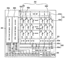
- FIG. 5 is a CMOS circuit diagram illustrating a configuration of an infrared detector using Sa-FPA according to an embodiment of the present invention.
- FIGS. 1 to 4 That is, the circuit diagram generated by FIGS. 1 to 4 is shown.
- reference cell bolometers 610a to 610n and / or active cell bolometers 620a to 620n are configured in the form of an array of columns and rows, each of which is a column. It is connected to the line and the low line.
- the first bolometer switching elements 630a to 630n are connected to each of the bolometers 620a to 620n to control on / off of each of the bolometers 620a to 620n.
- the column line control shift register 600a, the row line control shift register 600b, and the column line select switches 640a to 640n are configured for on / off control of the first bolometer switching elements 630a to 630n.
- the column line control shift register 600a is a 16-bit shift register that sequentially applies an address to the column line select switches 640a to 640n so that the column line select switches 640a to 640n sequentially select the column lines. Make it possible.
- the row line control shift register 600b is a 240-bit shift register that can sequentially turn on / off the active cell bolometers 620a to 620n in the row line by applying addresses one row line sequentially.
- the column line selection switches 640a to 640n may correspond to the output multiplexer unit described above.
- the column line selection switches 640a to 640n may be operated at the same time by blocking a predetermined number.
- one block may be formed in 20 units.
- the column line control shift register 600a sequentially enables the column line select switches 640a to 640n one by one while one row line is enabled by the row line control shift register 600b. do.
- the total time that all of the column line selection switches 640a to 640n are sequentially enabled is the same as the time when one row line is enabled.
- output pads Out 0 to Out 19 are formed in the analog current signal output unit 330.
- An external test device for example, the Agilent 4072A & UF3000
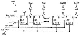
- FIG. 6 is a circuit diagram of the row control shift register 600b in the circuit diagram shown in FIG.
- the row control shift register 600b may include 240 flip-flops 1000, and the flip-flop 1000 may be implemented as a D-flip flop.
- the present invention is not limited thereto, and other types of flip flops are also possible.
- the flip flop 1000 is connected to the low signal line 1010, the low clock line 1020, and the reset line 1030.
- a control signal such as a low signal, a low clock, and a reset is input through the lines 1010, 1020, and 1030 connected to the analog current signal output unit 330 as shown in FIG. 5.
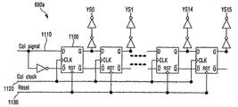
- FIG. 7 is a circuit diagram of a column control shift register in the circuit diagram shown in FIG. 5.
- the column control shift register 600b may include 16 flip-flops 1100, and the flip-flop 1100 may be implemented as a D-flip flop.
- the present invention is not limited thereto, and other types of flip flops are also possible.
- the flip flop 1100 is connected to the column signal line 1110, the low clock line 1120, and the reset line 1130.
- FIG. 8 is another circuit diagram illustrating a configuration of an infrared ray sensor using Sa-FPA according to another embodiment of the present invention. Unlike FIG. 5, FIG. 8 does not use shift registers 600a and 600b, but uses the multiplexers 1200a and 1200b to form row and column lines constituting an array of a predetermined size (eg, 320 ⁇ 240). It has a characteristic of applying an address to the.
- a predetermined size eg, 320 ⁇ 240
- the column line control multiplexer 1200a is configured as a multiplexer (MUX) (for example, a 4x6 bit multiplexer), and selectively applies an address to a column line to select a column line selection switch 640a to 640n in a corresponding column line. ) On / off.
- MUX multiplexer
- the row line control multiplexer 1200b is composed of a multiplexer (MUX) (for example, an 8x240 bit multiplexer), and a bolometer switching element 630a to 630n in a corresponding row line by selectively applying an address to the row line. Turn on / off.
- MUX multiplexer
- 8x240 bit multiplexer for example, an 8x240 bit multiplexer
- bolometer switching element 630a to 630n in a corresponding row line by selectively applying an address to the row line. Turn on / off.
- the bolometer switching elements 630a to 630n it is possible to selectively test randomly the bolometer switching elements 630a to 630n.
- the cells may be sequentially selected and tested.
- the column line control multiplexer 1200a sequentially enables the column line select switches 640a to 640n one by one while one row line is enabled by the row line control multiplexer 1200b.
- the total time that all of the column line selection switches 640a to 640n are sequentially enabled is the same as the time when one row line is enabled.
- the inverting switching elements 1210a to 1210n are provided in the reference cell bolometers 610a to 610n.
- the inverting switching device a PMOS transistor or the like may be used.
- a first column line connection pad 1225 and a second row line connection pad 1223 may be formed in the analog current signal output unit 330 to directly select a column line and / or a row line.
- a first signal output connection pad 1227 or the like for outputting an electrical signal (ie, analog data) generated by the bolometers 610a to 610n and / or 630a to 630n is configured.
- Each of the first signal output connection pads 1227 is connected in a one-to-one correspondence with each of the routing lines 650a to 650n.
- FIG. 9 is a block diagram illustrating an operation mode and a test mode of an infrared detector according to an exemplary embodiment of the present invention.
- the bolometer 120 is composed of a pixel array, which is composed of a reference cell 610 and an active cell 620.
- the row line selection unit 600b may correspond to the row line control shift register 600b of FIG. 5, and the output multiplexer unit 600a may be controlled by the column control shift register 600a of FIG. 5.
- the output multiplexer 320 may be referred to as a general concept.
- the output multiplexer 600a and the row line selector 600b are components formed in the basic logic / switch circuit board 110.
- the external application signal AX generated from the external Sa-FPA controller chip 200 or the tester may be input to the row line selector 600b.
- the external application signal AX from the external Sa-FPA controller chip 200 may be transmitted to the infrared sensor chip 100.
- the row line selector 600b receives the externally applied signal AX and generates an internal signal XS so as to correspond thereto.
- Each cell constituting the active cell 620 may be turned on / off by this internal signal XS.
- the external authorization signal AY may also be input to the output multiplexer unit 600a.
- the external authorization signal (AY) may also be transmitted from the external Sa-FPA controller chip 200 or the tester.
- the output multiplexer unit 600a may be implemented as a multiplexer MUX having a predetermined size, and each multiplexer MUX may be selected by an external application signal AY.
- 10 and 11 are circuit diagrams illustrating the configuration of the bolometer 120 and the output multiplexer unit 600a in the block diagram of FIG. 9.
- one end of the reference cell 610 may be connected to the first terminal VSK, and the other end may be selectively connected to the output multiplexer unit 600a.
- a variable analog power source controlled by the DAC from outside the chip may be applied to the first terminal VSK, but is not limited thereto.
- it may be supplied from an external Sa-FPA controller chip 200 (see FIG. 1), and at this time, the Sa-FPA controller chip 200 may be integrated with a DAC variable analog power chip.
- the selective connection between the other end of the reference cell 610 and the output multiplexer unit 600a may be achieved by the first switch P1.
- One end of the first switch P1 is connected to one end of the reference cell 610, and the other end is connected to one input terminal of the output multiplexer unit 600a and may be turned on / off according to the control signal GSK.
- the control signal GSK may be an analog power control signal controlled by a DAC from outside the chip, but is not limited thereto.
- One end of the active cell 620 may be selectively connected to the second terminal VSSA, and the other end may be selectively connected to the other end of the first switch P1.
- An analog power source controlled by the DAC may be applied to the second terminal VSSA from the outside of the chip, but is not limited thereto.
- Selective connection between one end of the active cell 620 and the second terminal VSSA may be achieved by the second switch N1.
- the second switch N1 may be turned on / off according to the control signal XS.
- the connection between the other end of the active cell 620 and the other end of the first switch P1 may be achieved by the third switch N2.
- the third switch N2 may be turned on / off according to the control signal VFID.
- the control signal VFID may be an analog control signal controlled by a DAC from outside the chip, but is not limited thereto.
- the other end of the active cell and the other end of the reference cell may be input to one input terminal of the output multiplexer unit 600a according to on / off of the first switch P1, the second switch N1, and the third switch N2. Can be.
- the first switch P1, the second switch N1, and the third switch N2 may be implemented as transistors, but may be implemented as other switch elements.
- the first switch P1 may be implemented as a PMOS transistor, and the second switch N1 and the third switch N2 may be implemented as an NMOS transistor, but vice versa.
- a case where the first switch P1 is implemented with a PMOS transistor and the second switch N1 and the third switch N2 are implemented with an NMOS transistor will be described as an example.
- the description of each signal (VSK, GSK, VFID, XS, VSSA) should be reversed.
- the signals VSK, GSK, VFID, XS, and VSSA may be analog control signals controlled by a DAC from outside the chip, but are not limited thereto. That is, in the following description, when the digital high signal is input to the first terminal VSK, in the opposite case (when PMOS and NMOS are interchanged), the digital low signal is input to the first terminal VSK. Should be.
- an external voltage is applied to the reference cell 610 and the active cell 620 independently, and the difference in signal current flowing through each of the cells 610 and 620 is output as it is or in an amplified state.
- a digital high signal may be input as the control signal XS to the second switch N1 connected to the active cell 620 that requires activation.
- an analog power source controlled by an external D / A converter may be input to the first terminal VSK, and a low signal may be input to the second terminal VSSA or may be connected to ground.
- control signals VFID and GSK of the first switch P1 and the third switch N2 an analog power source controlled by an appropriate external D / A converter can be input.
- a current having a predetermined magnitude flows through the reference cell 610 and the active cell 620 according to the control signals VFID and GSK applied to the first switch P1 and the third switch N2.
- FIG. 12 is a circuit diagram of FIG. 10, in which the first switch P1 and the third switch N2 operate in the saturation region of the transistor, and the second switch N1 operates in the linear region. It is a circuit diagram showing.
- the first switch P1 and the third switch N2 operate in the saturation region of the transistor, and the second switch N1 operates in the linear region.
- the difference I1-I2 between the current I1 flowing in the reference cell 610 and the current I2 flowing in the active cell 620 is input to one input terminal of the output multiplexer unit 600a.
- the difference I1-I2 of the current may be input as it is, or may be input in an amplified state through a simple current amplifier. That is, a simple amplifier, for example, a current amplifier using a current mirror (not shown) may be further formed in front of the output multiplexer unit 600a.
- the output multiplexer unit 600a may output the corresponding input signal according to the external authorization signal AY.
- an element (not shown) for amplifying the difference between the currents may be further included at the front end of the input terminal of the output multiplexer unit 600a.
- the resistance values of the reference cell 610 and the active cell 620 are respectively measured for statistical monitoring, whether the sensor is defective or not, and a good die is selected.
- a digital high signal may be input as the control signal XS to the second switch N1 connected to the active cell 620 to be tested.
- a digital high signal is input to the first terminal VSK, and is low as the control signals GSK and VFID of the first switch P1 and the third switch N2. You can input a signal. Accordingly, the first switch P1 is turned on and the third switch N2 is turned off. In this case, a current value flowing through the reference cell 610 may be input to one input terminal of the output multiplexer unit 600a, and a corresponding input value may be output from the output multiplexer unit 600a by an external application signal AY. have.
- the resistance value of the reference cell 610 can be known from the signal output through the output multiplexer 600a, that is, the current flowing through the reference cell 610. have. At this time, of course, the ON resistance of the first switch should be much smaller than that of the reference cell.
- a high signal may be input as the control signals GSK and VFID of the first switch P1 and the third switch N2.
- a low signal may be input to the second terminal VSSA or may be connected to ground.
- the first switch P1 is turned off and the third switch N2 is turned on. That is, it operates in the linear region of the transistor. Since a high signal is input as the control signal XS to the second switch N1 connected to the active cell 620 to be tested, a current value flowing through the active cell 620 is one of the output multiplexer 600a.
- the input terminal may be input to the input terminal, and a corresponding input value may be output from the output multiplexer unit 600a by an external authorization signal AY. Since the voltage value across the active cell 620 is known, the resistance value of the active cell 620 can be known from the signal output through the output multiplexer 600a, that is, the current flowing through the active cell 620. have. At this time, the ON resistance of the second and third switches should be much smaller than that of the active cell.
Landscapes
- Physics & Mathematics (AREA)
- General Physics & Mathematics (AREA)
- Spectroscopy & Molecular Physics (AREA)
- Photometry And Measurement Of Optical Pulse Characteristics (AREA)
- Semiconductor Integrated Circuits (AREA)
- Solid State Image Pick-Up Elements (AREA)
Priority Applications (4)
| Application Number | Priority Date | Filing Date | Title |
|---|---|---|---|
| US13/997,262 US20140014827A1 (en) | 2011-03-04 | 2012-03-05 | Infrared sensor chip, infrared detector and method for oeprating and testing the same |
| EP12748373.3A EP2546623A4 (de) | 2011-03-04 | 2012-03-05 | Infrarotsensorchip, infrarotdetektor sowie betriebsverfahren und testverfahren dafür |
| KR1020137009494A KR101519607B1 (ko) | 2011-03-04 | 2012-03-05 | 적외선 센서칩, 적외선 감지기, 이의 동작 방법 및 테스트 방법 |
| CN201280000480.0A CN103026193B (zh) | 2011-03-04 | 2012-03-05 | 红外线传感器芯片、红外线检测器以及其运行方法和测试方法 |
Applications Claiming Priority (2)
| Application Number | Priority Date | Filing Date | Title |
|---|---|---|---|
| KR10-2011-0019687 | 2011-03-04 | ||
| KR1020110019687A KR20120100643A (ko) | 2011-03-04 | 2011-03-04 | Sa-FPA를 이용한 적외선 감지기 및 이의 제조 방법 |
Publications (2)
| Publication Number | Publication Date |
|---|---|
| WO2012121526A2 true WO2012121526A2 (ko) | 2012-09-13 |
| WO2012121526A3 WO2012121526A3 (ko) | 2012-12-27 |
Family
ID=46798638
Family Applications (1)
| Application Number | Title | Priority Date | Filing Date |
|---|---|---|---|
| PCT/KR2012/001612 WO2012121526A2 (ko) | 2011-03-04 | 2012-03-05 | 적외선 센서칩, 적외선 감지기, 이의 동작 방법 및 테스트 방법 |
Country Status (5)
| Country | Link |
|---|---|
| US (1) | US20140014827A1 (de) |
| EP (1) | EP2546623A4 (de) |
| KR (2) | KR20120100643A (de) |
| CN (1) | CN103026193B (de) |
| WO (1) | WO2012121526A2 (de) |
Cited By (3)
| Publication number | Priority date | Publication date | Assignee | Title |
|---|---|---|---|---|
| WO2014093724A1 (en) * | 2012-12-14 | 2014-06-19 | Flir Systems, Inc. | Segmented focal plane array architecture |
| US9918023B2 (en) | 2010-04-23 | 2018-03-13 | Flir Systems, Inc. | Segmented focal plane array architecture |
| US9948878B2 (en) | 2010-04-23 | 2018-04-17 | Flir Systems, Inc. | Abnormal clock rate detection in imaging sensor arrays |
Families Citing this family (3)
| Publication number | Priority date | Publication date | Assignee | Title |
|---|---|---|---|---|
| FR3009388B1 (fr) * | 2013-07-30 | 2015-07-17 | Ulis | Diagnostic de l'etat defectueux d'une matrice de detection bolometrique |
| CN104269465B (zh) * | 2014-09-30 | 2016-12-07 | 中国空空导弹研究院 | 焦平面探测器相连缺陷元的识别方法与测试基片 |
| JP7147468B2 (ja) * | 2018-10-26 | 2022-10-05 | 富士通株式会社 | 赤外線検出器の読み出し回路及びその検査方法 |
Family Cites Families (8)
| Publication number | Priority date | Publication date | Assignee | Title |
|---|---|---|---|---|
| US5808350A (en) * | 1997-01-03 | 1998-09-15 | Raytheon Company | Integrated IR, visible and NIR sensor and methods of fabricating same |
| WO2006122529A2 (de) * | 2005-05-17 | 2006-11-23 | Heimann Sensor Gmbh | Thermopile infrarot sensorarray |
| KR100765158B1 (ko) * | 2006-02-16 | 2007-10-15 | 주식회사 오카스 | 적외선 신호 검출 회로 및 검출 방법 |
| WO2007135850A1 (ja) * | 2006-05-24 | 2007-11-29 | The Ritsumeikan Trust | 赤外線アレイセンサ |
| JP4978501B2 (ja) * | 2008-02-14 | 2012-07-18 | 日本電気株式会社 | 熱型赤外線検出器及びその製造方法 |
| FR2936052B1 (fr) * | 2008-09-16 | 2014-09-05 | Ulis | Dispositif pur la detection d'un rayonnement infrarouge comportant un bolometre resistif d'imagerie, systeme comprenant une matrice de tels bolometres, et procede de lecture d'un bolometre d'imagerie integre dans un tel system |
| CA2767023C (en) * | 2011-02-09 | 2014-09-09 | Research In Motion Limited | Increased low light sensitivity for image sensors by combining quantum dot sensitivity to visible and infrared light |
| US8436305B1 (en) * | 2011-03-16 | 2013-05-07 | Magnolia Optical Technologies, Inc. | Infrared radiation sensing device using a carbon nanotube and polymer composition and method of making the same |
-
2011
- 2011-03-04 KR KR1020110019687A patent/KR20120100643A/ko active Search and Examination
-
2012
- 2012-03-05 US US13/997,262 patent/US20140014827A1/en not_active Abandoned
- 2012-03-05 WO PCT/KR2012/001612 patent/WO2012121526A2/ko active Application Filing
- 2012-03-05 CN CN201280000480.0A patent/CN103026193B/zh active Active
- 2012-03-05 KR KR1020137009494A patent/KR101519607B1/ko active IP Right Grant
- 2012-03-05 EP EP12748373.3A patent/EP2546623A4/de not_active Withdrawn
Non-Patent Citations (2)
| Title |
|---|
| None |
| See also references of EP2546623A4 |
Cited By (4)
| Publication number | Priority date | Publication date | Assignee | Title |
|---|---|---|---|---|
| US9918023B2 (en) | 2010-04-23 | 2018-03-13 | Flir Systems, Inc. | Segmented focal plane array architecture |
| US9948878B2 (en) | 2010-04-23 | 2018-04-17 | Flir Systems, Inc. | Abnormal clock rate detection in imaging sensor arrays |
| US11070747B2 (en) | 2010-04-23 | 2021-07-20 | Flir Systems, Inc. | Segmented focal plane array architecture |
| WO2014093724A1 (en) * | 2012-12-14 | 2014-06-19 | Flir Systems, Inc. | Segmented focal plane array architecture |
Also Published As
| Publication number | Publication date |
|---|---|
| KR101519607B1 (ko) | 2015-05-15 |
| US20140014827A1 (en) | 2014-01-16 |
| KR20130057482A (ko) | 2013-05-31 |
| CN103026193B (zh) | 2017-04-05 |
| KR20120100643A (ko) | 2012-09-12 |
| WO2012121526A3 (ko) | 2012-12-27 |
| CN103026193A (zh) | 2013-04-03 |
| EP2546623A4 (de) | 2014-07-23 |
| EP2546623A2 (de) | 2013-01-16 |
Similar Documents
| Publication | Publication Date | Title |
|---|---|---|
| WO2012121526A2 (ko) | 적외선 센서칩, 적외선 감지기, 이의 동작 방법 및 테스트 방법 | |
| JP4351632B2 (ja) | センサ配置およびセンサ配置の駆動方法 | |
| US6362618B1 (en) | Hall sensor for stress and temperature measurements in addition to magnetic field measurement | |
| US20080018324A1 (en) | Voltage-impressed current measuring apparatus and current buffers with switches used therefor | |
| JP4174511B2 (ja) | 半導体集積回路の雑音検出及び測定回路 | |
| KR100485462B1 (ko) | 집적회로검사방법 | |
| JP2007527535A (ja) | 半導体素子試験用の2チャンネルソース測定ユニット | |
| US10222231B2 (en) | Apparatus and method for sensing | |
| WO2020135257A1 (zh) | 一种能减少漏电流的可寻址测试芯片及其测试系统 | |
| WO2014148706A1 (ko) | 아날로그 센서의 종류 판별 장치 | |
| KR19990072932A (ko) | 복잡한회로구성없이정확하게테스트할수있는디지털/아날로그변환기,이를이용한반도체집적회로및그테스트방법 | |
| US7221170B2 (en) | Semiconductor test circuit | |
| WO2020135258A1 (zh) | 一种能提高电阻测量精度的可寻址测试芯片及其测试系统 | |
| JP5193635B2 (ja) | 半導体装置 | |
| JP2007017229A (ja) | マルチチップモジュール | |
| JP2009133762A (ja) | 半導体装置およびその試験方法 | |
| JP2011222547A (ja) | テストエレメントグループおよび半導体装置 | |
| WO2022103232A1 (ko) | 신소자 테스트 시스템 및 신소자 테스트 방법 | |
| KR19990062211A (ko) | 반도체 장치의 테스트 시스템 | |
| JP4034242B2 (ja) | オープン検査回路を備えた半導体装置及び該検査回路を用いたオープン検査方法 | |
| JP4480880B2 (ja) | 半導体回路 | |
| Pieńczuk et al. | Multichannel Programmable Readout IC for Photodiodes Array | |
| KR20100076723A (ko) | 다종의 센서 어레이용 신호 처리 회로 | |
| JP2009065037A (ja) | 半導体集積回路とその検査装置 | |
| JP2002214280A (ja) | 半導体試験装置 |
Legal Events
| Date | Code | Title | Description |
|---|---|---|---|
| WWE | Wipo information: entry into national phase |
Ref document number: 201280000480.0 Country of ref document: CN |
|
| WWE | Wipo information: entry into national phase |
Ref document number: 2012748373 Country of ref document: EP |
|
| 121 | Ep: the epo has been informed by wipo that ep was designated in this application |
Ref document number: 12748373 Country of ref document: EP Kind code of ref document: A2 |
|
| ENP | Entry into the national phase |
Ref document number: 20137009494 Country of ref document: KR Kind code of ref document: A |
|
| NENP | Non-entry into the national phase |
Ref country code: DE |
|
| WWE | Wipo information: entry into national phase |
Ref document number: 13997262 Country of ref document: US |