WO2012121141A1 - Ceramic multilayered substrate and manufacturing method for same - Google Patents
Ceramic multilayered substrate and manufacturing method for same Download PDFInfo
- Publication number
- WO2012121141A1 WO2012121141A1 PCT/JP2012/055364 JP2012055364W WO2012121141A1 WO 2012121141 A1 WO2012121141 A1 WO 2012121141A1 JP 2012055364 W JP2012055364 W JP 2012055364W WO 2012121141 A1 WO2012121141 A1 WO 2012121141A1
- Authority
- WO
- WIPO (PCT)
- Prior art keywords
- ceramic
- electrode
- electrode paste
- multilayer substrate
- green sheet
- Prior art date
Links
Images


Classifications
-
- B—PERFORMING OPERATIONS; TRANSPORTING
- B32—LAYERED PRODUCTS
- B32B—LAYERED PRODUCTS, i.e. PRODUCTS BUILT-UP OF STRATA OF FLAT OR NON-FLAT, e.g. CELLULAR OR HONEYCOMB, FORM
- B32B18/00—Layered products essentially comprising ceramics, e.g. refractory products
-
- B—PERFORMING OPERATIONS; TRANSPORTING
- B32—LAYERED PRODUCTS
- B32B—LAYERED PRODUCTS, i.e. PRODUCTS BUILT-UP OF STRATA OF FLAT OR NON-FLAT, e.g. CELLULAR OR HONEYCOMB, FORM
- B32B3/00—Layered products comprising a layer with external or internal discontinuities or unevennesses, or a layer of non-planar form; Layered products having particular features of form
- B32B3/26—Layered products comprising a layer with external or internal discontinuities or unevennesses, or a layer of non-planar form; Layered products having particular features of form characterised by a particular shape of the outline of the cross-section of a continuous layer; characterised by a layer with cavities or internal voids ; characterised by an apertured layer
- B32B3/266—Layered products comprising a layer with external or internal discontinuities or unevennesses, or a layer of non-planar form; Layered products having particular features of form characterised by a particular shape of the outline of the cross-section of a continuous layer; characterised by a layer with cavities or internal voids ; characterised by an apertured layer characterised by an apertured layer, the apertures going through the whole thickness of the layer, e.g. expanded metal, perforated layer, slit layer regular cells B32B3/12
-
- H—ELECTRICITY
- H05—ELECTRIC TECHNIQUES NOT OTHERWISE PROVIDED FOR
- H05K—PRINTED CIRCUITS; CASINGS OR CONSTRUCTIONAL DETAILS OF ELECTRIC APPARATUS; MANUFACTURE OF ASSEMBLAGES OF ELECTRICAL COMPONENTS
- H05K3/00—Apparatus or processes for manufacturing printed circuits
- H05K3/10—Apparatus or processes for manufacturing printed circuits in which conductive material is applied to the insulating support in such a manner as to form the desired conductive pattern
- H05K3/12—Apparatus or processes for manufacturing printed circuits in which conductive material is applied to the insulating support in such a manner as to form the desired conductive pattern using thick film techniques, e.g. printing techniques to apply the conductive material or similar techniques for applying conductive paste or ink patterns
- H05K3/1258—Apparatus or processes for manufacturing printed circuits in which conductive material is applied to the insulating support in such a manner as to form the desired conductive pattern using thick film techniques, e.g. printing techniques to apply the conductive material or similar techniques for applying conductive paste or ink patterns by using a substrate provided with a shape pattern, e.g. grooves, banks, resist pattern
-
- H—ELECTRICITY
- H05—ELECTRIC TECHNIQUES NOT OTHERWISE PROVIDED FOR
- H05K—PRINTED CIRCUITS; CASINGS OR CONSTRUCTIONAL DETAILS OF ELECTRIC APPARATUS; MANUFACTURE OF ASSEMBLAGES OF ELECTRICAL COMPONENTS
- H05K3/00—Apparatus or processes for manufacturing printed circuits
- H05K3/46—Manufacturing multilayer circuits
- H05K3/4611—Manufacturing multilayer circuits by laminating two or more circuit boards
- H05K3/4626—Manufacturing multilayer circuits by laminating two or more circuit boards characterised by the insulating layers or materials
- H05K3/4629—Manufacturing multilayer circuits by laminating two or more circuit boards characterised by the insulating layers or materials laminating inorganic sheets comprising printed circuits, e.g. green ceramic sheets
-
- Y—GENERAL TAGGING OF NEW TECHNOLOGICAL DEVELOPMENTS; GENERAL TAGGING OF CROSS-SECTIONAL TECHNOLOGIES SPANNING OVER SEVERAL SECTIONS OF THE IPC; TECHNICAL SUBJECTS COVERED BY FORMER USPC CROSS-REFERENCE ART COLLECTIONS [XRACs] AND DIGESTS
- Y10—TECHNICAL SUBJECTS COVERED BY FORMER USPC
- Y10T—TECHNICAL SUBJECTS COVERED BY FORMER US CLASSIFICATION
- Y10T428/00—Stock material or miscellaneous articles
- Y10T428/24—Structurally defined web or sheet [e.g., overall dimension, etc.]
- Y10T428/24273—Structurally defined web or sheet [e.g., overall dimension, etc.] including aperture
- Y10T428/24322—Composite web or sheet
Definitions
- the present invention relates to a ceramic multilayer substrate and a manufacturing method thereof, and more particularly to a ceramic multilayer substrate provided with at least one of an internal electrode and a surface electrode and a manufacturing method thereof.
- Ceramic multilayer substrates usually have a structure in which electrodes (surface electrodes, internal electrodes) are provided on the surface and inside of a ceramic substrate (substrate body) on which a plurality of ceramic layers are laminated.
- the present invention solves the above-mentioned problems, and even when surface electrodes and internal electrodes are arranged at a high density with a narrow interval, occurrence of short-circuiting due to oozing or jumping out between adjacent surface electrodes or internal electrodes.
- the present invention provides a method for manufacturing a ceramic multilayer substrate capable of efficiently manufacturing a highly reliable ceramic multilayer substrate that can suppress and prevent the above, and a highly reliable ceramic multilayer substrate manufactured by the manufacturing method For the purpose.
- the ceramic multilayer substrate of the present invention comprises: In a ceramic multilayer substrate comprising a ceramic substrate formed by laminating a plurality of ceramic layers, and an electrode disposed in the ceramic layer, The main surface of any one of the ceramic layers is characterized in that a recess is formed by the electrode and the surrounding ceramic layer.
- a method of providing a recess formed by the electrode and the surrounding ceramic layer for example, (a) an electrode paste having a large amount of sintering shrinkage is used for forming the electrode, and the electrode paste is intended at the time of firing.
- a groove that becomes a recess is formed in advance around the area where the electrode paste of the ceramic green sheet is to be printed by a method such as laser processing.
- Forming the electrode paste pattern by printing the electrode paste on the region surrounded by the groove, and (d) marking the electrode paste on the ceramic green sheet
- the electrode paste pattern formed by, for example, a method of forming a groove as a concave portion by a method such as laser processing are illustrated, it is also possible to use still other methods.
- the surface of the ceramic substrate constituting the ceramic multilayer substrate is often provided with various surface electrodes (electrodes, wirings, etc.) at high density.
- the present invention is applied to the surface of the ceramic substrate.
- the ceramic multilayer substrate of the present invention another ceramic layer is laminated on the ceramic layer in which the concave portion is formed, so that the gap between the electrode and the surrounding ceramic layer is increased. It is preferable that voids are formed.
- the electrode is preferably embedded in the ceramic layer.
- the recess is formed on the surface of a ceramic layer constituting the outermost layer of the ceramic substrate, the electrode forming the recess is a surface electrode, and a peripheral portion of the surface electrode is covered It is preferably covered with a ceramic layer.
- the method for producing the ceramic multilayer substrate of the present invention includes: A method for producing a ceramic multilayer substrate comprising a ceramic substrate formed by laminating a plurality of ceramic layers, and an electrode disposed on the ceramic layer, (a) preparing a ceramic green sheet; (b) a step of printing a resin paste around a region of the ceramic green sheet on which an electrode paste for electrode formation is printed; (c) forming an electrode paste pattern by printing an electrode paste on a region of the ceramic green sheet surrounded by the resin paste; (d) laminating the ceramic green sheets on which the electrode paste pattern is formed to form a laminate; and (e) firing the laminate.
- the periphery of the area where the electrode paste pattern is formed on the ceramic green sheet is covered with the resin paste, and the electrode paste oozes out.
- the resin paste burns, decomposes and disappears, so that a recess is formed between the electrode and the ceramic layer.
- a reliable ceramic multilayer substrate that is less likely to cause a short circuit between surface electrodes or between internal electrodes is reliably manufactured. It becomes possible to do.
- the method for manufacturing a ceramic multilayer substrate according to the present invention when forming a laminate by laminating ceramic green sheets having an electrode paste pattern in which a recess is formed in the periphery, (a) the above electrode paste A ceramic green sheet having a pattern, and (b) a ceramic green sheet different from that in the above (a), and an electrode paste pattern provided with an electrode paste pattern not particularly configured to form a recess around the periphery It is possible to use a suitable combination of ceramic green sheets or the like not formed, and the present invention includes such an embodiment.
- a method for producing a ceramic multilayer substrate comprising a ceramic substrate formed by laminating a plurality of ceramic layers, and an electrode disposed on the ceramic layer, (a) preparing a ceramic green sheet; (b) forming a groove around a region of the ceramic green sheet where an electrode paste for electrode formation is printed; (c) forming an electrode paste pattern by printing an electrode paste on a region surrounded by the groove of the ceramic green sheet; (d) laminating the ceramic green sheets on which the electrode paste pattern is formed to form a laminate; and (e) firing the laminate.
- a method for producing a ceramic multilayer substrate comprising a ceramic substrate formed by laminating a plurality of ceramic layers, and an electrode disposed on the ceramic layer, (a) preparing a ceramic green sheet; (b) printing an electrode paste on the ceramic green sheet to form an electrode paste pattern; (c) forming a groove around the electrode paste pattern of the ceramic green sheet; (d) laminating the ceramic green sheets with the grooves formed around the electrode paste pattern to form a laminate; and (e) firing the laminate.
- the ceramic green sheet on which the electrode paste pattern to be the surface electrode of the ceramic substrate is formed covers at least the peripheral portion of the electrode paste pattern, and the central portion is covered. It is preferable to dispose a coated ceramic green layer that is not covered and to form the laminate using this ceramic green sheet. By providing this configuration, it becomes possible to obtain a ceramic multilayer substrate having a structure in which the peripheral portion of the surface electrode is covered with the coated ceramic layer. In addition to the basic effect of the present invention, the peel strength of the surface electrode Therefore, it is possible to reliably manufacture a ceramic multilayer substrate with higher reliability.
- the ceramic multilayer substrate of the present invention is a ceramic multilayer substrate comprising a ceramic substrate formed by laminating a plurality of ceramic layers, and an electrode disposed on the ceramic layer. Since the concave portion is formed by the surrounding ceramic layer, it is possible to suppress or prevent the occurrence of a short circuit between the surface electrodes and between the internal electrodes due to the exudation or protrusion of the electrodes.
- a multilayer substrate can be provided.
- FIG. 1 It is front sectional drawing which shows the structure of the ceramic multilayer substrate concerning one Example of this invention. It is a figure which expands and shows the principal part of the ceramic multilayer substrate concerning the Example of this invention.
- (a)-(c) is a figure explaining the manufacturing method (manufacturing method A) of the ceramic multilayer substrate concerning the Example of this invention.
- (a)-(c) is a figure explaining the manufacturing method (manufacturing method B) of the ceramic multilayer substrate concerning the Example of this invention.
- (a)-(c) is a figure explaining the manufacturing method (manufacturing method C) of the ceramic multilayer substrate concerning the Example of this invention.
- (a)-(c) is a figure explaining the manufacturing method (manufacturing method D) of the ceramic multilayer substrate concerning the Example of this invention.
- (a)-(c) is a figure explaining the manufacturing method (manufacturing method E) of the ceramic multilayer substrate concerning the Example of this invention.
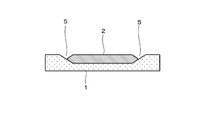
- FIG. 1 is a cross-sectional view schematically showing the overall configuration of a ceramic multilayer substrate 20 according to an embodiment of the present invention
- FIG. 2 is a cross-sectional view showing the main part thereof.
- a ceramic multilayer substrate 20 is a ceramic multilayer substrate mounted on a mounting substrate, and includes a ceramic substrate 10 having a structure in which a plurality of ceramic layers (base ceramic layers) 1 are laminated, and a ceramic.
- a surface electrode 2 disposed on a ceramic layer 1 constituting the outermost layer of the substrate and an internal electrode 3 disposed on a predetermined ceramic layer 1 are provided.
- predetermined ones of the surface electrode 2 and the internal electrode 3 are connected to each other through a via-hole conductor 4.
- this ceramic multilayer substrate 20 As shown in FIGS. 1 and 2, between the surface electrode 2 and the surrounding ceramic layer 1 and between the internal electrode 3 and the surrounding ceramic layer 1.
- a recess 5 is provided.
- the recess 5 is formed by the surface electrode 2 and the surrounding ceramic layer 1 or by the internal electrode 3 and the surrounding ceramic layer 1. Since another ceramic layer 1 is laminated on the recess 5 formed by the internal electrode 3 and the surrounding ceramic layer 1, a gap is formed in the recess 5.
- the multilayer ceramic electronic component of Example 1 has the above-described configuration, and the concave portion 5 is provided between the surface electrode 2 and the internal electrode 3 and the surrounding ceramic layer 1. For example, it is possible to surely prevent a short circuit from occurring between adjacent electrodes due to bleeding or jumping out of the surface electrode 2 and the internal electrode 3. As a result, even when the distance between the electrodes such as the surface electrode 2 and the internal electrode 3 is narrowed (that is, the electrodes such as the surface electrode 2 and the internal electrode 3 are densified), there is no short-circuit between the electrodes and reliability. High ceramic multilayer substrate 20 can be obtained.
- each of the surface electrode and the internal electrode is configured to have a recess around the periphery, but the surface electrode formed on the surface of the ceramic substrate in which the electrodes are normally arranged at high density is used. Even when the concave portion is formed only around the periphery, a highly reliable ceramic multilayer substrate can be obtained.
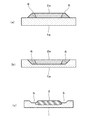
- an electrode paste pattern 2a is formed by printing an electrode paste on the ceramic green sheet 1a.
- an electrode paste having a shrinkage rate (sintering shrinkage rate) in the firing process larger than that of the ceramic green sheet 1a is used as the electrode paste for forming the electrode paste pattern 2a.
- the ceramic green sheet 1a on which the electrode paste pattern 2a is printed is laminated and pressed to form a laminate.
- the electrode paste pattern 2a disposed on the ceramic green sheet 1a is pressed and deformed, and is buried in the ceramic green sheet 1a as schematically shown in FIG. 3 (b). It becomes.
- 3 (a) and 3 (b) show a ceramic green sheet 1a constituting the outermost layer of the laminate, and an electrode paste pattern 2a to be formed on the surface electrode 2 (see FIGS. 1 and 2) after firing.
- the electrode paste pattern that forms the internal electrode is similarly deformed to have a shape similar to the shape schematically shown in FIG.
- the sintering shrinkage rate is used as an electrode paste for forming an electrode paste pattern that becomes a surface electrode after firing.
- an electrode paste larger than the sintering shrinkage rate of the ceramic green sheet 1a may be used.
- the sintering shrinkage rate is used as an electrode paste for forming an electrode paste pattern that becomes an internal electrode after firing.
- an electrode paste larger than the sintering shrinkage rate of the ceramic green sheet 1a may be used.
- the ceramic material constituting the ceramic substrate and the constituent material and composition of the electrode paste it is necessary to appropriately select the ceramic material constituting the ceramic substrate and the constituent material and composition of the electrode paste, but specifically, it is actually used. It is desirable to appropriately select a ceramic material and additive components constituting the ceramic substrate, a conductive component constituting the electrode paste, an additive component such as glass, and the like in consideration of materials and characteristics required for the ceramic multilayer substrate. For example, if the ratio of the glass contained in the material constituting the ceramic substrate and the electrode paste is large, the glass component may ooze out and fill the recess, so it is usually preferable that the ratio of the glass component is small. .
- the electrode paste pattern 2a is formed by printing the electrode paste on the region surrounded by the resin paste 6 of the ceramic green sheet 1a.
- the ceramic green sheet 1a on which the electrode paste pattern 2a is formed is laminated and pressed to form a laminate.
- the electrode paste pattern 2a and the resin paste 6 disposed on the ceramic green sheet 1a are pressed and deformed, and as schematically shown in FIG. 4B, the ceramic green sheet 1a. It will be in the state buried in.
- FIGS. 1 and 2 show a ceramic green sheet 1a constituting the outermost layer of the laminate, and an electrode paste pattern 2a formed thereon and used as a surface electrode 2 (see FIGS. 1 and 2) after firing.
- the resin paste 6 is shown, the electrode paste pattern that forms the internal electrode and the resin paste disposed around the electrode paste pattern located inside the laminated body are also laminated and pressed in the same manner. It is deformed to have a shape similar to the shape schematically shown in FIG.
- an electrode paste pattern that becomes a surface electrode after firing is provided.
- the resin paste may be printed around the area where the electrode paste pattern is to be formed.
- an electrode paste pattern that becomes an internal electrode after firing is provided.
- the resin paste may be printed around the area where the electrode paste pattern is to be formed. Since another ceramic layer is formed on the concave portion formed around the internal electrode, a void is formed in the concave portion.
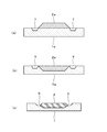
- grooves 7 are formed by laser processing around the area of the ceramic green sheet 1a where the electrode paste for electrode formation is printed.
- the electrode paste pattern 2a is formed by printing the electrode paste on the region surrounded by the groove 7 of the ceramic green sheet 1a.
- the electrode paste pattern 2a is printed on the inner region of the groove 7, the ceramic green sheet 1a is laminated, and the laminate is formed by pressure bonding. In this lamination and pressure bonding process, the electrode paste pattern 2a disposed on the ceramic green sheet 1a is pressed and deformed, and is embedded in the ceramic green sheet 1a as schematically shown in FIG. 5 (b). It becomes.
- FIGS. 1 and 2 show a ceramic green sheet 1a constituting the outermost layer of the laminate, and an electrode paste pattern 2a formed thereon and used as a surface electrode 2 (see FIGS. 1 and 2) after firing.
- the electrode paste pattern that forms the internal electrode is similarly deformed to have a shape similar to the shape schematically shown in FIG.
- the groove 7 is formed around the region of the ceramic green sheet 1a where the electrode paste for electrode formation is printed, and then the electrode paste is printed in the region surrounded by the groove 7 to form the electrode paste pattern 2a.
- the electrode paste pattern 2a is formed by printing the electrode paste on the ceramic green sheet 1a before forming the groove 7, and then the electrode paste of the ceramic green sheet 1a is formed. It is also possible to form the groove 7 around the area where the pattern 2a is formed.
- the groove 7 is formed after the electrode paste pattern 2a is formed, even if there is some oozing or popping out in the process of forming the electrode paste pattern 2a, it is removed in the process of forming the groove 7 Is done. As a result, even when surface electrodes and internal electrodes are arranged at high density at narrow intervals, a reliable ceramic multilayer substrate that is less likely to cause a short circuit between surface electrodes or between internal electrodes is reliably manufactured. It becomes possible to do.
- an electrode paste pattern that becomes a surface electrode after firing is provided.
- the groove may be formed only for the ceramic green sheet.
- an electrode paste pattern that becomes an internal electrode after firing is provided.
- the groove may be formed only for the ceramic green sheet. Since another ceramic layer is formed on the concave portion formed around the internal electrode, a void is formed in the concave portion.
- the electrode paste pattern 2a is formed by printing the electrode paste on the region surrounded by the resin paste 6 of the ceramic green sheet 1a.
- the ceramic green sheet on which the electrode paste pattern 2a to be the surface electrode 2 (see FIGS. 1 and 2) is formed, as shown in FIG. 6 (a), at least the peripheral portion of the electrode paste pattern 2a is provided.
- a coated ceramic green layer 8a that covers and does not cover the central portion is disposed.
- a ceramic paste is used, the resin paste 6 is covered from the peripheral portion of the electrode paste pattern 2a, and the ceramic paste is printed in a range reaching the exposed area of the ceramic green sheet 1a, thereby forming the coated ceramic green layer 8a.
- the ceramic used for the ceramic paste it is desirable to use a ceramic to which glass or an oxide is further added in order to increase the adhesion strength, centering on a ceramic having the same composition as that of the ceramic constituting the underlying ceramic substrate.
- the ceramic used for the ceramic paste may be a mixture of barium oxide, silicon oxide, alumina, calcium oxide, and boron oxide.
- the ceramic constituting the ceramic substrate serving as the base is a ferrite type, it is desirable to use ferrite powder.
- a method of laminating ceramic green sheets provided with an opening that exposes the central portion of the electrode paste pattern to be the surface electrode may be used. Is possible.
- a ceramic green sheet (not shown) provided with an electrode paste pattern to be an internal electrode is prepared by the same method as described in the manufacturing method B of [2] above.
- the ceramic green sheet 1a on which the coated ceramic green layer 8a is formed and the ceramic green sheet provided with the electrode paste pattern serving as an internal electrode are laminated and bonded to form a laminate.
- the electrode paste pattern 2a, the resin paste 6, and the coated ceramic green layer 8a disposed on the ceramic green sheet 1a are pressed and deformed, as schematically shown in FIG. 6 (b). In addition, it is buried in the ceramic green sheet 1a.
- the electrode paste pattern serving as an internal electrode has a shape as schematically shown in FIG. 4B used for explaining the manufacturing method B of [2] above.
- the laminate produced in the step (5) is fired.
- the resin paste 6 burns, decomposes and disappears, and as shown in FIG. 6C, a recess 5 is formed around the surface electrode 2 formed after firing, and the surface A ceramic multilayer substrate having a structure in which the peripheral edge of the electrode 2 is covered with the coated ceramic layer 8 obtained by firing the coated ceramic green layer 8a is obtained. Since the recess 5 formed by the surface electrode 2 and the surrounding ceramic layer 1 is covered with the coating ceramic layer 8, a gap is formed in the recess 5.
- the ceramic paste is not printed around the electrode paste pattern to be the internal electrode.
- the internal electrode is reliably covered between the ceramic layers, so that it is particularly covered. Even if the ceramic layer is not formed, the required reliability is ensured.
- the surface electrode 2 has a structure in which the peripheral portion of the surface electrode 2 is covered with the coating ceramic layer 8 and only the center portion of the surface electrode 2 is exposed. A ceramic multilayer substrate having an excellent peel strength of 2 is obtained.
- the electrode paste pattern 2a is formed by printing the electrode paste on the ceramic green sheet 1a.
- the ceramic green sheet 1a on which the electrode paste pattern 2a to be the surface electrode 2 (see FIGS. 1 and 2) is formed as shown in FIG. 7A, at least the periphery of the electrode paste pattern 2a A coated ceramic green layer 8a that covers the portion and does not cover the center portion is disposed.
- the coated ceramic green layer 8a is formed by printing the same ceramic paste as used in the manufacturing method D of [4] above.
- the electrode paste pattern 2a and the coated ceramic green layer 8a disposed on the ceramic green sheet 1a are pressed and deformed, and as shown schematically in FIG. It is buried in the sheet 1a, and the upper surface thereof is substantially flush with the upper surfaces of the surrounding ceramic green sheet 1a and the electrode paste pattern 2a.
- the electrode paste pattern 2a shrinks in the direction along the main surface, and as shown in FIG. 7C, between the surrounding ceramic layer (ceramic layer formed by firing the ceramic green sheet 1a) 1 Ceramic multilayer substrate having a structure in which a recess 5 is formed and a peripheral portion of the surface electrode 2 formed by firing the electrode paste pattern 2a is coated with the coated ceramic layer 8 formed by firing the coated ceramic green layer 8a Is obtained. Since the recess 5 formed by the surface electrode 2 and the surrounding ceramic layer 1 is covered with the coating ceramic layer 8, a gap is formed in the recess 5.
- the surface electrode 2 has a structure in which the peripheral edge portion of the surface electrode is covered with the covering ceramic layer 8 and only the central portion of the surface electrode 2 is exposed.
- a ceramic multilayer substrate having excellent peel strength can be obtained.
- the present invention is not limited to the above-described embodiments, and relates to a specific configuration of the ceramic substrate, an arrangement mode and constituent material of the internal electrode, a specific pattern of the surface electrode, and the like within the scope of the invention. It is possible to add various applications and modifications.
Abstract
Provided is a manufacturing method for a ceramic multilayered substrate, and a high reliability ceramic multilayered substrate manufactured using this method. The method enables efficient manufacturing of a high reliability ceramic multilayered substrate that has no shorting between adjacent electrodes even if surface electrodes and internal electrodes are arranged with high density. A ceramic multilayered substrate (20) provided with a ceramic substrate (10) formed of a plurality of stacked ceramic layers (1) and with electrodes (surface electrodes (2) and internal electrodes (3)) disposed in the ceramic layers (1), wherein on the main surfaces of any of the ceramic layers recesses (5) are provided constituted by the electrodes and the ceramic layer (1) surrounding the electrodes. The electrodes (surface electrodes (2) and internal electrodes (3)) are buried in the ceramic layer (1). Outer edges of the surface electrodes (2) are covered with a covering ceramic layer.
Description
本発明はセラミック多層基板およびその製造方法に関し、詳しくは、内部電極および表面電極の少なくとも一方を備えたセラミック多層基板およびその製造方法に関する。
The present invention relates to a ceramic multilayer substrate and a manufacturing method thereof, and more particularly to a ceramic multilayer substrate provided with at least one of an internal electrode and a surface electrode and a manufacturing method thereof.
セラミック多層基板は、通常、複数のセラミック層が積層されたセラミック基板(基板本体)の表面および内部に電極(表面電極、内部電極)を備えた構造を有している。
Ceramic multilayer substrates usually have a structure in which electrodes (surface electrodes, internal electrodes) are provided on the surface and inside of a ceramic substrate (substrate body) on which a plurality of ceramic layers are laminated.
このようなセラミック多層基板においては、小型化が進むにつれて、表面電極や内部電極を狭い間隔で高密度に配設することが必要になり、隣り合う表面電極間、あるいは、内部電極間のショート(短絡)が問題となる。
In such a ceramic multilayer substrate, as the miniaturization progresses, it is necessary to dispose the surface electrodes and the internal electrodes at a high density at a narrow interval, and a short circuit between adjacent surface electrodes or between the internal electrodes ( Short circuit) becomes a problem.
このような問題を解決する方法として、表面電極や内部電極を形成するために用いられる導電性ペーストの組成を調整して、表面電極や内部電極に滲みが発生することを抑制、防止して、電極間のショートが生じないようにしたセラミック回路基板(セラミック多層基板)の製造方法が提案されている(特許文献1参照)。
As a method of solving such a problem, by adjusting the composition of the conductive paste used to form the surface electrode and the internal electrode, to suppress and prevent the occurrence of bleeding on the surface electrode and the internal electrode, A method of manufacturing a ceramic circuit board (ceramic multilayer board) in which no short-circuit between electrodes has occurred has been proposed (see Patent Document 1).
しかしながら、特許文献1の方法では、導電性ペーストを印刷することにより形成される表面電極や内部電極となるパターンの全体としての滲み出しを抑制することはできても、突発的、局所的な滲み出しや飛び出しの発生を防止することは困難である。この局所的な電極の滲み出しや飛び出しは、印刷機へのパターンのまわりこみや版離れなどに起因して生じるものであり、導電性ペーストそのものを変更しても避けられないものもある。また、印刷パターンや印刷機を改善しても、量産工程においては、局所的、突発的な滲み出しや飛び出しは避けられない場合もあるのが実情である。
However, in the method of Patent Document 1, even though it is possible to suppress the overall bleeding of the pattern that becomes the surface electrode and the internal electrode formed by printing the conductive paste, sudden and localized bleeding It is difficult to prevent the occurrence of sticking out or popping out. This local oozing or popping of the electrode is caused by pattern sneaking into the printing press or separation of the plate, and there are some cases that cannot be avoided even if the conductive paste itself is changed. In addition, even if the printing pattern and the printing machine are improved, in the mass production process, local and sudden oozing and popping may be unavoidable.
本発明は、上記課題を解決するものであり、表面電極や内部電極を狭い間隔で高密度に配設した場合にも、隣り合う表面電極間や内部電極間の滲み出しや飛び出しによるショートの発生を抑制、防止することが可能で、信頼性の高いセラミック多層基板を効率よく製造することが可能なセラミック多層基板の製造方法および該製造方法により製造される信頼性の高いセラミック多層基板を提供することを目的とする。
The present invention solves the above-mentioned problems, and even when surface electrodes and internal electrodes are arranged at a high density with a narrow interval, occurrence of short-circuiting due to oozing or jumping out between adjacent surface electrodes or internal electrodes. The present invention provides a method for manufacturing a ceramic multilayer substrate capable of efficiently manufacturing a highly reliable ceramic multilayer substrate that can suppress and prevent the above, and a highly reliable ceramic multilayer substrate manufactured by the manufacturing method For the purpose.
上記課題を解決するために、本発明のセラミック多層基板は、
複数のセラミック層を積層してなるセラミック基板と、前記セラミック層に配設された電極とを備えたセラミック多層基板において、
いずれかの前記セラミック層の主面に、前記電極とその周囲の前記セラミック層とにより凹部が形成されていること
を特徴としている。
なお、電極と、その周囲のセラミック層とにより形成される凹部を設ける方法としては、例えば、(a)電極の形成に、焼結収縮量の大きな電極ペーストを用い、焼成時に電極ペーストを意図するような程度に収縮させることにより、電極の周囲に凹部を形成する方法、(b)焼成工程で消失する樹脂ペーストなどの消失材料を電極パターンの周囲に配設した状態で焼成を行い、焼成工程で消失材料を消失させることにより、電極の周囲に凹部を形成する方法、(c)セラミックグリーンシートの電極ペーストを印刷する領域の周囲に、例えばレーザー加工などの方法により、凹部となる溝を予め形成しておき、溝に囲われた領域に電極ペーストを印刷して電極ペーストパターンを形成する方法、 (d)セラミックグリーンシート上に電極ペーストを印刷して形成した電極ペーストパターンの周囲に、例えばレーザー加工などの方法により凹部となる溝を形成する方法 などが例示されるが、さらに他の方法を用いることも可能である。また、セラミック多層基板を構成するセラミック基板の表面は、種々の表面電極(電極や配線など)が高密度に配設される場合が多いが、そのような場合に本発明を適用して、表面電極の周囲に凹部を設けることにより、隣り合う表面電極間のショートを抑制して、表面電極を高密度に配設した場合にも高い信頼性を備えたセラミック多層基板を得ることができる。 In order to solve the above problems, the ceramic multilayer substrate of the present invention comprises:
In a ceramic multilayer substrate comprising a ceramic substrate formed by laminating a plurality of ceramic layers, and an electrode disposed in the ceramic layer,
The main surface of any one of the ceramic layers is characterized in that a recess is formed by the electrode and the surrounding ceramic layer.
As a method of providing a recess formed by the electrode and the surrounding ceramic layer, for example, (a) an electrode paste having a large amount of sintering shrinkage is used for forming the electrode, and the electrode paste is intended at the time of firing. A method of forming a recess around the electrode by shrinking to such a degree, (b) firing in a state where a disappearing material such as a resin paste disappearing in the firing step is disposed around the electrode pattern, and a firing step (C) A groove that becomes a recess is formed in advance around the area where the electrode paste of the ceramic green sheet is to be printed by a method such as laser processing. Forming the electrode paste pattern by printing the electrode paste on the region surrounded by the groove, and (d) marking the electrode paste on the ceramic green sheet Around the electrode paste pattern formed by, for example, a method of forming a groove as a concave portion by a method such as laser processing are illustrated, it is also possible to use still other methods. In addition, the surface of the ceramic substrate constituting the ceramic multilayer substrate is often provided with various surface electrodes (electrodes, wirings, etc.) at high density. In such a case, the present invention is applied to the surface of the ceramic substrate. By providing the recesses around the electrodes, a short circuit between adjacent surface electrodes can be suppressed, and a ceramic multilayer substrate having high reliability can be obtained even when the surface electrodes are arranged with high density.
また、本発明のセラミック多層基板においては、前記凹部が形成された前記セラミック層の上に、さらに別のセラミック層が積層されることにより、前記電極とその周囲の前記セラミック層との間には空隙が形成されていることが好ましい。
Further, in the ceramic multilayer substrate of the present invention, another ceramic layer is laminated on the ceramic layer in which the concave portion is formed, so that the gap between the electrode and the surrounding ceramic layer is increased. It is preferable that voids are formed.
また、前記電極は前記セラミック層に埋没していることが好ましい。
この構成を備えることにより、セラミック多層基板の低背化を図ることができる。
また、前記凹部は、前記セラミック基板の最外層を構成するセラミック層の表面に形成されたものであり、前記凹部を形成する前記電極は表面電極であって、前記表面電極の周縁部は、被覆セラミック層により覆われていることが好ましい。この構成を備えることにより、上述の効果に加えて、表面電極の剥離強度が向上するという効果が得られる。 The electrode is preferably embedded in the ceramic layer.
By providing this configuration, it is possible to reduce the height of the ceramic multilayer substrate.
Further, the recess is formed on the surface of a ceramic layer constituting the outermost layer of the ceramic substrate, the electrode forming the recess is a surface electrode, and a peripheral portion of the surface electrode is covered It is preferably covered with a ceramic layer. By providing this configuration, in addition to the above-described effects, the effect of improving the peel strength of the surface electrode can be obtained.
また、本発明のセラミック多層基板の製造方法は、
複数のセラミック層を積層してなるセラミック基板と、前記セラミック層に配設された電極とを備えたセラミック多層基板の製造方法であって、
(a)セラミックグリーンシートを準備する工程と、
(b)前記セラミックグリーンシートの、電極形成用の電極ペーストが印刷される領域の周囲に樹脂ペーストを印刷する工程と、
(c)前記セラミックグリーンシートの、前記樹脂ペーストにより囲われた領域に電極ペーストを印刷して電極ペーストパターンを形成する工程と、
(d)前記電極ペーストパターンが形成された前記セラミックグリーンシートを積層して積層体を形成する工程と、
(e)前記積層体を焼成する工程と
を具備することを特徴としている。
この構成を備えることにより、電極ペーストを印刷して電極ペーストパターンを形成する工程では、セラミックグリーンシートの電極ペーストパターンが形成される領域の周囲が樹脂ペーストにより被覆されており、電極ペーストの滲み出しや飛び出しそのものが抑えられ、また、滲み出しや飛び出しがあったとしても、樹脂ペースト上への滲み出しや飛び出しとなる。また、焼成工程では、樹脂ペーストが燃焼、分解して消失することにより、電極の周囲の、セラミック層との間に凹部が形成される。その結果、電極(例えば表面電極や内部電極など)の滲み出しや飛び出しにより、隣り合う表面電極間や内部電極間にショートが発生することを効果的に抑制、防止することが可能になる。その結果、表面電極や内部電極などを狭い間隔で高密度に配設した場合にも、表面電極間や内部電極間にショートが発生するおそれの少ない、信頼性の高いセラミック多層基板を確実に製造することが可能になる。なお、本発明のセラミック多層基板の製造方法において、周囲に凹部が形成されるような電極ペーストパターンを備えたセラミックグリーンシートを積層して積層体を形成するにあたっては、(a)上述の電極ペーストパターンを備えたセラミックグリーンシートに、(b)特に周囲に凹部が形成されるように構成されていない電極ペーストパターンを備えた、上記(a)のものとは異なるセラミックグリーンシートや、電極ペーストパターンの形成されていないセラミックグリーンシートなどを適宜組み合わせて用いることが可能であり、本発明はそのような態様も含むものである。 Moreover, the method for producing the ceramic multilayer substrate of the present invention includes:
A method for producing a ceramic multilayer substrate comprising a ceramic substrate formed by laminating a plurality of ceramic layers, and an electrode disposed on the ceramic layer,
(a) preparing a ceramic green sheet;
(b) a step of printing a resin paste around a region of the ceramic green sheet on which an electrode paste for electrode formation is printed;
(c) forming an electrode paste pattern by printing an electrode paste on a region of the ceramic green sheet surrounded by the resin paste;
(d) laminating the ceramic green sheets on which the electrode paste pattern is formed to form a laminate;
and (e) firing the laminate.
With this configuration, in the step of forming the electrode paste pattern by printing the electrode paste, the periphery of the area where the electrode paste pattern is formed on the ceramic green sheet is covered with the resin paste, and the electrode paste oozes out. In addition, even if there is a ooze or pop-out, it will ooze out or jump out onto the resin paste. In the firing step, the resin paste burns, decomposes and disappears, so that a recess is formed between the electrode and the ceramic layer. As a result, it is possible to effectively suppress or prevent the occurrence of a short circuit between adjacent surface electrodes or between internal electrodes due to the exudation or protrusion of electrodes (for example, surface electrodes or internal electrodes). As a result, even when surface electrodes and internal electrodes are arranged at high density at narrow intervals, a reliable ceramic multilayer substrate that is less likely to cause a short circuit between surface electrodes or between internal electrodes is reliably manufactured. It becomes possible to do. In the method for manufacturing a ceramic multilayer substrate according to the present invention, when forming a laminate by laminating ceramic green sheets having an electrode paste pattern in which a recess is formed in the periphery, (a) the above electrode paste A ceramic green sheet having a pattern, and (b) a ceramic green sheet different from that in the above (a), and an electrode paste pattern provided with an electrode paste pattern not particularly configured to form a recess around the periphery It is possible to use a suitable combination of ceramic green sheets or the like not formed, and the present invention includes such an embodiment.
また、本発明の他のセラミック多層基板の製造方法は、
複数のセラミック層を積層してなるセラミック基板と、前記セラミック層に配設された電極とを備えたセラミック多層基板の製造方法であって、
(a)セラミックグリーンシートを準備する工程と、
(b)前記セラミックグリーンシートの、電極形成用の電極ペーストが印刷される領域の周囲に溝を形成する工程と、
(c)前記セラミックグリーンシートの、前記溝により囲われた領域に電極ペーストを印刷して電極ペーストパターンを形成する工程と、
(d)前記電極ペーストパターンが形成された前記セラミックグリーンシートを積層して積層体を形成する工程と、
(e)前記積層体を焼成する工程と
を具備することを特徴としている。
この構成を備えることにより、電極ペーストパターンを形成する際の、滲み出し部分や飛び出し部分が溝(凹部)に落ち込んで、溝よりも外側に達することが抑制、防止され、ショート不良の発生する可能性が大幅に軽減される。その結果、表面電極や内部電極などを狭い間隔で高密度に配設した場合にも、表面電極間や内部電極間にショートが発生するおそれの少ない、信頼性の高いセラミック多層基板を確実に製造することが可能になる。 In addition, another method for manufacturing a ceramic multilayer substrate of the present invention is as follows.
A method for producing a ceramic multilayer substrate comprising a ceramic substrate formed by laminating a plurality of ceramic layers, and an electrode disposed on the ceramic layer,
(a) preparing a ceramic green sheet;
(b) forming a groove around a region of the ceramic green sheet where an electrode paste for electrode formation is printed;
(c) forming an electrode paste pattern by printing an electrode paste on a region surrounded by the groove of the ceramic green sheet;
(d) laminating the ceramic green sheets on which the electrode paste pattern is formed to form a laminate;
and (e) firing the laminate.
By having this configuration, when the electrode paste pattern is formed, it is possible to prevent or prevent a bleed portion or a protruding portion from dropping into the groove (concave portion) and reaching the outside of the groove, thereby causing a short circuit failure. Sex is greatly reduced. As a result, even when surface electrodes and internal electrodes are arranged at high density at narrow intervals, a reliable ceramic multilayer substrate that is less likely to cause a short circuit between surface electrodes or between internal electrodes is reliably manufactured. It becomes possible to do.
また、本発明のさらに他のセラミック多層基板の製造方法は、
複数のセラミック層を積層してなるセラミック基板と、前記セラミック層に配設された電極とを備えたセラミック多層基板の製造方法であって、
(a)セラミックグリーンシートを準備する工程と、
(b)前記セラミックグリーンシートに電極ペーストを印刷して電極ペーストパターンを形成する工程と、
(c)前記セラミックグリーンシートの、前記電極ペーストパターンの周囲に溝を形成する工程と、
(d)前記電極ペーストパターンの周囲に前記溝が形成された前記セラミックグリーンシートを積層して積層体を形成する工程と、
(e)前記積層体を焼成する工程と
を具備することを特徴としている。
この構成を備えることにより、電極ペーストを印刷して電極ペーストパターンを形成する工程で多少の滲み出しや飛び出しがあった場合にも、それが溝を形成する工程で除去される。その結果、表面電極や内部電極などを狭い間隔で高密度に配設した場合にも、表面電極間や内部電極間にショートが発生するおそれの少ない、信頼性の高いセラミック多層基板を確実に製造することが可能になる。 In addition, another method for producing a ceramic multilayer substrate of the present invention is as follows.
A method for producing a ceramic multilayer substrate comprising a ceramic substrate formed by laminating a plurality of ceramic layers, and an electrode disposed on the ceramic layer,
(a) preparing a ceramic green sheet;
(b) printing an electrode paste on the ceramic green sheet to form an electrode paste pattern;
(c) forming a groove around the electrode paste pattern of the ceramic green sheet;
(d) laminating the ceramic green sheets with the grooves formed around the electrode paste pattern to form a laminate;
and (e) firing the laminate.
By providing this configuration, even if there is some oozing or popping out in the step of forming the electrode paste pattern by printing the electrode paste, it is removed in the step of forming the groove. As a result, even when surface electrodes and internal electrodes are arranged at high density at narrow intervals, a reliable ceramic multilayer substrate that is less likely to cause a short circuit between surface electrodes or between internal electrodes is reliably manufactured. It becomes possible to do.
また、本発明のセラミック多層基板の製造方法においては、前記セラミック基板の表面電極となる電極ペーストパターンが形成されたセラミックグリーンシートについては、前記電極ペーストパターンの少なくとも周縁部を被覆し、中央部を被覆しない被覆セラミックグリーン層を配設し、このセラミックグリーンシートを用いて前記積層体を形成することが好ましい。
この構成を備えることにより、表面電極の周縁部が被覆セラミック層により覆われた構造を有するセラミック多層基板を得ることが可能になり、本発明の基本的な効果に加えて、表面電極の剥離強度が大きく、より信頼性の高いセラミック多層基板を確実に製造することが可能になる。なお、表面電極となる電極ペーストパターンの少なくとも周縁部を被覆し、中央部を被覆しない被覆セラミックグリーン層は、例えば、セラミックペーストを、電極ペーストパターンの少なくとも周縁部を被覆し、中央部は露出させるような態様で印刷したり、表面電極となる電極ペーストパターンの中央部を露出させるような開口を設けたセラミックグリーンシートを積層したりする方法により形成することが可能である。 In the method for producing a ceramic multilayer substrate of the present invention, the ceramic green sheet on which the electrode paste pattern to be the surface electrode of the ceramic substrate is formed covers at least the peripheral portion of the electrode paste pattern, and the central portion is covered. It is preferable to dispose a coated ceramic green layer that is not covered and to form the laminate using this ceramic green sheet.
By providing this configuration, it becomes possible to obtain a ceramic multilayer substrate having a structure in which the peripheral portion of the surface electrode is covered with the coated ceramic layer. In addition to the basic effect of the present invention, the peel strength of the surface electrode Therefore, it is possible to reliably manufacture a ceramic multilayer substrate with higher reliability. The coated ceramic green layer that covers at least the peripheral portion of the electrode paste pattern to be the surface electrode and does not cover the central portion covers, for example, the ceramic paste and at least the peripheral portion of the electrode paste pattern, and exposes the central portion. It is possible to form by printing in such a manner, or by laminating ceramic green sheets provided with an opening that exposes the central portion of the electrode paste pattern to be the surface electrode.
本発明のセラミック多層基板は、複数のセラミック層を積層してなるセラミック基板と、セラミック層に配設された電極とを備えたセラミック多層基板において、いずれかのセラミック層の主面に、電極とその周囲のセラミック層とにより凹部を形成するようにしているので、電極などの滲み出しや飛び出しによる、表面電極間や内部電極間のショートの発生を抑制、防止することが可能になる。
The ceramic multilayer substrate of the present invention is a ceramic multilayer substrate comprising a ceramic substrate formed by laminating a plurality of ceramic layers, and an electrode disposed on the ceramic layer. Since the concave portion is formed by the surrounding ceramic layer, it is possible to suppress or prevent the occurrence of a short circuit between the surface electrodes and between the internal electrodes due to the exudation or protrusion of the electrodes.
その結果、表面電極や内部電極を狭い間隔で高密度に配設した場合にも、隣り合う表面電極間や内部電極間のショートの発生を抑制、防止することが可能で、信頼性の高いセラミック多層基板を提供することができる。
As a result, even when surface electrodes and internal electrodes are arranged with high density at narrow intervals, it is possible to suppress and prevent the occurrence of short circuits between adjacent surface electrodes or internal electrodes, and a highly reliable ceramic. A multilayer substrate can be provided.
以下に本発明の実施例を示して、本発明の特徴とするところをさらに詳しく説明する。
Hereinafter, the features of the present invention will be described in more detail with reference to examples of the present invention.
[セラミック多層基板の構成]
図1は、本発明の実施例にかかるセラミック多層基板20の全体構成を模式的に示す断面図、図2はその要部を示す断面図である。 [Configuration of ceramic multilayer substrate]
FIG. 1 is a cross-sectional view schematically showing the overall configuration of aceramic multilayer substrate 20 according to an embodiment of the present invention, and FIG. 2 is a cross-sectional view showing the main part thereof.
図1は、本発明の実施例にかかるセラミック多層基板20の全体構成を模式的に示す断面図、図2はその要部を示す断面図である。 [Configuration of ceramic multilayer substrate]
FIG. 1 is a cross-sectional view schematically showing the overall configuration of a
この実施例1にかかるセラミック多層基板20は、実装基板上に実装されるセラミック多層基板であって、複数のセラミック層(基材セラミック層)1が積層された構造を有するセラミック基板10と、セラミック基板の最外層を構成するセラミック層1に配設された表面電極2と、所定のセラミック層1に配設された内部電極3を備えている。なお、表面電極2や内部電極3のうち所定のものはビヤホール導体4を介して層間接続されている。
A ceramic multilayer substrate 20 according to the first embodiment is a ceramic multilayer substrate mounted on a mounting substrate, and includes a ceramic substrate 10 having a structure in which a plurality of ceramic layers (base ceramic layers) 1 are laminated, and a ceramic. A surface electrode 2 disposed on a ceramic layer 1 constituting the outermost layer of the substrate and an internal electrode 3 disposed on a predetermined ceramic layer 1 are provided. In addition, predetermined ones of the surface electrode 2 and the internal electrode 3 are connected to each other through a via-hole conductor 4.
そして、このセラミック多層基板20においては、図1および2に示すように、表面電極2とその周囲のセラミック層1との間、および、内部電極3とその周囲のセラミック層1との間には凹部5が設けられている。凹部5は、表面電極2とその周囲のセラミック層1により、または、内部電極3とその周囲のセラミック層1により、形成されている。また、内部電極3とその周囲のセラミック層1とにより形成された凹部5の上には、別のセラミック層1が積層されているので、当該凹部5の部分には空隙が形成されている。
In this ceramic multilayer substrate 20, as shown in FIGS. 1 and 2, between the surface electrode 2 and the surrounding ceramic layer 1 and between the internal electrode 3 and the surrounding ceramic layer 1. A recess 5 is provided. The recess 5 is formed by the surface electrode 2 and the surrounding ceramic layer 1 or by the internal electrode 3 and the surrounding ceramic layer 1. Since another ceramic layer 1 is laminated on the recess 5 formed by the internal electrode 3 and the surrounding ceramic layer 1, a gap is formed in the recess 5.
この実施例1の積層セラミック電子部品は、上述のような構成を備えており、表面電極2および内部電極3とその周囲のセラミック層1との間に凹部5が設けられているので、電極(例えば表面電極2や内部電極3など)の滲み出しや飛び出しにより、隣り合う電極間にショートが発生することを確実に抑制することが可能になる。その結果、表面電極2や内部電極3などの電極間の間隔を狭くした(すなわち表面電極2や内部電極3などの電極を高密度化)した場合にも、電極間のショートのない、信頼性の高いセラミック多層基板20を得ることができる。
The multilayer ceramic electronic component of Example 1 has the above-described configuration, and the concave portion 5 is provided between the surface electrode 2 and the internal electrode 3 and the surrounding ceramic layer 1. For example, it is possible to surely prevent a short circuit from occurring between adjacent electrodes due to bleeding or jumping out of the surface electrode 2 and the internal electrode 3. As a result, even when the distance between the electrodes such as the surface electrode 2 and the internal electrode 3 is narrowed (that is, the electrodes such as the surface electrode 2 and the internal electrode 3 are densified), there is no short-circuit between the electrodes and reliability. High ceramic multilayer substrate 20 can be obtained.
なお、この実施例では、表面電極および内部電極のいずれもが、周囲に凹部を備えた構成としているが、通常は電極が高密度で配設されるセラミック基板の表面に形成される表面電極の周囲にのみ凹部が形成されるように構成した場合にも、信頼性の高いセラミック多層基板を得ることが可能になる。
In this embodiment, each of the surface electrode and the internal electrode is configured to have a recess around the periphery, but the surface electrode formed on the surface of the ceramic substrate in which the electrodes are normally arranged at high density is used. Even when the concave portion is formed only around the periphery, a highly reliable ceramic multilayer substrate can be obtained.
[セラミック多層基板の製造]
次に、本発明のセラミック多層基板の製造方法について説明する。 [Manufacture of ceramic multilayer substrates]
Next, the manufacturing method of the ceramic multilayer substrate of this invention is demonstrated.
次に、本発明のセラミック多層基板の製造方法について説明する。 [Manufacture of ceramic multilayer substrates]
Next, the manufacturing method of the ceramic multilayer substrate of this invention is demonstrated.
[1]製造方法A
図3(a)~(c)を参照しつつ、セラミック多層基板の製造方法Aについて説明する。 [1] Manufacturing method A
A method A for manufacturing a ceramic multilayer substrate will be described with reference to FIGS.
図3(a)~(c)を参照しつつ、セラミック多層基板の製造方法Aについて説明する。 [1] Manufacturing method A
A method A for manufacturing a ceramic multilayer substrate will be described with reference to FIGS.
(1)まず、セラミックグリーンシートを準備する。
(1) First, prepare a ceramic green sheet.
(2)それから、図3(a)に示すように、セラミックグリーンシート1aに、電極ペーストを印刷して電極ペーストパターン2aを形成する。
このとき電極ペーストパターン2aを形成するための電極ペーストとして、焼成工程での収縮率(焼結収縮率)が、セラミックグリーンシート1aの焼結収縮率よりも大きい電極ペーストを用いる。 (2) Then, as shown in FIG. 3A, anelectrode paste pattern 2a is formed by printing an electrode paste on the ceramic green sheet 1a.
At this time, as the electrode paste for forming theelectrode paste pattern 2a, an electrode paste having a shrinkage rate (sintering shrinkage rate) in the firing process larger than that of the ceramic green sheet 1a is used.
このとき電極ペーストパターン2aを形成するための電極ペーストとして、焼成工程での収縮率(焼結収縮率)が、セラミックグリーンシート1aの焼結収縮率よりも大きい電極ペーストを用いる。 (2) Then, as shown in FIG. 3A, an
At this time, as the electrode paste for forming the
(3)電極ペーストパターン2aが印刷されたセラミックグリーンシート1aを積層し、圧着することにより積層体を形成する。
この積層、圧着の工程で、セラミックグリーンシート1aに配設された電極ペーストパターン2aは、押圧されて変形し、図3(b)に模式的に示すように、セラミックグリーンシート1aに埋没した状態となる。 (3) The ceramicgreen sheet 1a on which the electrode paste pattern 2a is printed is laminated and pressed to form a laminate.
In this lamination and pressure bonding process, theelectrode paste pattern 2a disposed on the ceramic green sheet 1a is pressed and deformed, and is buried in the ceramic green sheet 1a as schematically shown in FIG. 3 (b). It becomes.
この積層、圧着の工程で、セラミックグリーンシート1aに配設された電極ペーストパターン2aは、押圧されて変形し、図3(b)に模式的に示すように、セラミックグリーンシート1aに埋没した状態となる。 (3) The ceramic
In this lamination and pressure bonding process, the
なお、図3(a),(b)は積層体の最外層を構成するセラミックグリーンシート1aと、そこに形成された焼成後に表面電極2(図1,2参照)となる電極ペーストパターン2aを示しているが、内部電極を形成することになる電極ペーストパターンも同様に変形して、図3(b)に模式的に示すような形状と同様の形状となる。
3 (a) and 3 (b) show a ceramic green sheet 1a constituting the outermost layer of the laminate, and an electrode paste pattern 2a to be formed on the surface electrode 2 (see FIGS. 1 and 2) after firing. Although shown, the electrode paste pattern that forms the internal electrode is similarly deformed to have a shape similar to the shape schematically shown in FIG.
(4)上記(3)の工程で作製した積層体を焼成する。
このとき、電極ペーストパターン2aが主面に沿う方向に収縮し、その周囲のセラミック層との間に凹部5が形成される。
これにより、表面電極2(および内部電極3)の周囲に凹部5が形成された、図1,2に示すようなセラミック多層基板20が得られる。 (4) The laminate produced in the step (3) is fired.
At this time, theelectrode paste pattern 2a shrinks in the direction along the main surface, and the recess 5 is formed between the electrode paste pattern 2a and the surrounding ceramic layer.
Thereby, theceramic multilayer substrate 20 as shown in FIGS. 1 and 2 in which the concave portion 5 is formed around the surface electrode 2 (and the internal electrode 3) is obtained.
このとき、電極ペーストパターン2aが主面に沿う方向に収縮し、その周囲のセラミック層との間に凹部5が形成される。
これにより、表面電極2(および内部電極3)の周囲に凹部5が形成された、図1,2に示すようなセラミック多層基板20が得られる。 (4) The laminate produced in the step (3) is fired.
At this time, the
Thereby, the
なお、セラミック基板の表面に形成される表面電極の周囲にのみ凹部が形成されるようにしたい場合には、焼成後に表面電極となる電極ペーストパターンを形成するための電極ペーストとして、焼結収縮率が、セラミックグリーンシート1aの焼結収縮率よりも大きい電極ペーストを用いるようにすればよい。
また、セラミック基板の内部に形成される内部電極の周囲にのみ凹部が形成されるようにしたい場合には、焼成後に内部電極となる電極ペーストパターンを形成するための電極ペーストとして、焼結収縮率が、セラミックグリーンシート1aの焼結収縮率よりも大きい電極ペーストを用いるようにすればよい。 In addition, when it is desired to form a recess only around the surface electrode formed on the surface of the ceramic substrate, the sintering shrinkage rate is used as an electrode paste for forming an electrode paste pattern that becomes a surface electrode after firing. However, an electrode paste larger than the sintering shrinkage rate of the ceramicgreen sheet 1a may be used.
In addition, when it is desired to form a recess only around the internal electrode formed inside the ceramic substrate, the sintering shrinkage rate is used as an electrode paste for forming an electrode paste pattern that becomes an internal electrode after firing. However, an electrode paste larger than the sintering shrinkage rate of the ceramicgreen sheet 1a may be used.
また、セラミック基板の内部に形成される内部電極の周囲にのみ凹部が形成されるようにしたい場合には、焼成後に内部電極となる電極ペーストパターンを形成するための電極ペーストとして、焼結収縮率が、セラミックグリーンシート1aの焼結収縮率よりも大きい電極ペーストを用いるようにすればよい。 In addition, when it is desired to form a recess only around the surface electrode formed on the surface of the ceramic substrate, the sintering shrinkage rate is used as an electrode paste for forming an electrode paste pattern that becomes a surface electrode after firing. However, an electrode paste larger than the sintering shrinkage rate of the ceramic
In addition, when it is desired to form a recess only around the internal electrode formed inside the ceramic substrate, the sintering shrinkage rate is used as an electrode paste for forming an electrode paste pattern that becomes an internal electrode after firing. However, an electrode paste larger than the sintering shrinkage rate of the ceramic
また、確実に凹部を形成するためには、セラミック基板を構成するセラミック材料と、電極ペーストの構成材料や組成などを適切に選択することが必要となるが、具体的には、実際に用いられる材料や、セラミック多層基板に求められる特性などを考慮して、セラミック基板を構成するセラミック材料や添加成分、電極ペーストを構成する導電成分やガラスなどの添加成分などを適宜選択することが望ましい。
例えば、セラミック基板を構成する材料および電極ペーストに含まれるガラスの割合が多いと、ガラス成分が染み出てきて凹部を埋めてしまう可能性があるため、通常、ガラス成分の割合は少ない方が好ましい。
また、セラミック多層基板を製造する際に、焼成時の収縮を抑制するための収縮抑制層を用いて焼成を行うことにより、導電性ペーストの収縮率が比較的小さい場合にも、電極パターンと、その周囲のセラミック層との間に上記凹部を確実に形成することが可能になる。したがって、収縮抑制層を用いて焼成を行うことで、導電性ペーストの選択の自由度を向上させることができる。 Moreover, in order to reliably form the recesses, it is necessary to appropriately select the ceramic material constituting the ceramic substrate and the constituent material and composition of the electrode paste, but specifically, it is actually used. It is desirable to appropriately select a ceramic material and additive components constituting the ceramic substrate, a conductive component constituting the electrode paste, an additive component such as glass, and the like in consideration of materials and characteristics required for the ceramic multilayer substrate.
For example, if the ratio of the glass contained in the material constituting the ceramic substrate and the electrode paste is large, the glass component may ooze out and fill the recess, so it is usually preferable that the ratio of the glass component is small. .
Further, when producing a ceramic multilayer substrate, by performing firing using a shrinkage suppression layer for suppressing shrinkage during firing, even when the shrinkage rate of the conductive paste is relatively small, the electrode pattern, It is possible to reliably form the recesses between the surrounding ceramic layers. Therefore, the degree of freedom in selecting the conductive paste can be improved by firing using the shrinkage suppression layer.
電極の焼結収縮を大きくする製造方法Aの場合、電極ペーストパターンに滲み出しや飛び出しがあっても、焼成工程で電極ペーストパターンが焼結収縮する際に形成される電極周囲の凹部により、滲み出し部分や飛び出し部分が電極から絶縁される(電極が島状に孤立する)ことになるため、ショート不良の発生を効率よく防止することができる。
In the case of manufacturing method A that increases the sintering shrinkage of the electrode, even if the electrode paste pattern oozes or jumps out, the bleed is caused by the recesses around the electrode formed when the electrode paste pattern sinters and shrinks in the firing process. Since the protruding portion and the protruding portion are insulated from the electrode (the electrode is isolated in an island shape), it is possible to efficiently prevent occurrence of a short circuit defect.
[2]製造方法B
図4(a)~(c)を参照しつつ、セラミック多層基板の他の製造方法Bについて説明する。 [2] Manufacturing method B
With reference to FIGS. 4A to 4C, another manufacturing method B of the ceramic multilayer substrate will be described.
図4(a)~(c)を参照しつつ、セラミック多層基板の他の製造方法Bについて説明する。 [2] Manufacturing method B
With reference to FIGS. 4A to 4C, another manufacturing method B of the ceramic multilayer substrate will be described.
(1)まず、セラミックグリーンシートを準備する。
(1) First, prepare a ceramic green sheet.
(2)それから、図4(a)に示すように、セラミックグリーンシート1aの、電極形成用の電極ペーストが印刷される領域の周囲に樹脂ペースト6を印刷する。
(2) Then, as shown in FIG. 4A, the resin paste 6 is printed around the area of the ceramic green sheet 1a where the electrode paste for electrode formation is printed.
(3)次に、図4(a)に示すように、セラミックグリーンシート1aの、樹脂ペースト6により囲われた領域に電極ペーストを印刷して電極ペーストパターン2aを形成する。
(4)電極ペーストパターン2aが形成されたセラミックグリーンシート1aを積層し、圧着することにより積層体を形成する。 (3) Next, as shown in FIG. 4A, theelectrode paste pattern 2a is formed by printing the electrode paste on the region surrounded by the resin paste 6 of the ceramic green sheet 1a.
(4) The ceramicgreen sheet 1a on which the electrode paste pattern 2a is formed is laminated and pressed to form a laminate.
(4)電極ペーストパターン2aが形成されたセラミックグリーンシート1aを積層し、圧着することにより積層体を形成する。 (3) Next, as shown in FIG. 4A, the
(4) The ceramic
この積層、圧着の工程で、セラミックグリーンシート1aに配設された電極ペーストパターン2a、樹脂ペースト6は、押圧されて変形し、図4(b)に模式的に示すように、セラミックグリーンシート1aに埋没した状態となる。
In this lamination and pressure bonding process, the electrode paste pattern 2a and the resin paste 6 disposed on the ceramic green sheet 1a are pressed and deformed, and as schematically shown in FIG. 4B, the ceramic green sheet 1a. It will be in the state buried in.
なお、図4(a),(b)は積層体の最外層を構成するセラミックグリーンシート1aと、そこに形成された、焼成後に表面電極2(図1,2参照)となる電極ペーストパターン2aおよび樹脂ペースト6を示しているが、積層体の内部に位置する、内部電極を形成することになる電極ペーストパターンおよびその周囲に配設された樹脂ペーストも、積層、圧着の工程で、同様に変形して、図4(b)に模式的に示すような形状と同様の形状となる。
4 (a) and 4 (b) show a ceramic green sheet 1a constituting the outermost layer of the laminate, and an electrode paste pattern 2a formed thereon and used as a surface electrode 2 (see FIGS. 1 and 2) after firing. Although the resin paste 6 is shown, the electrode paste pattern that forms the internal electrode and the resin paste disposed around the electrode paste pattern located inside the laminated body are also laminated and pressed in the same manner. It is deformed to have a shape similar to the shape schematically shown in FIG.
(5)上記(4)の工程で作製した積層体を焼成する。
この焼成工程で、樹脂ペースト6は燃焼、分解して、消失し、図4(c)に示すように、焼成後に形成される表面電極2(および内部電極3)の周囲には、凹部5が形成される。
これにより、図1,2に示すセラミック多層基板20に準じる構造を有するセラミック多層基板が得られる。 (5) The laminate produced in the step (4) is fired.
In this firing step, theresin paste 6 burns, decomposes and disappears, and as shown in FIG. 4C, a recess 5 is formed around the surface electrode 2 (and the internal electrode 3) formed after firing. It is formed.
Thereby, a ceramic multilayer substrate having a structure according to theceramic multilayer substrate 20 shown in FIGS.
この焼成工程で、樹脂ペースト6は燃焼、分解して、消失し、図4(c)に示すように、焼成後に形成される表面電極2(および内部電極3)の周囲には、凹部5が形成される。
これにより、図1,2に示すセラミック多層基板20に準じる構造を有するセラミック多層基板が得られる。 (5) The laminate produced in the step (4) is fired.
In this firing step, the
Thereby, a ceramic multilayer substrate having a structure according to the
なお、セラミック基板の表面に形成される表面電極の周囲にのみ凹部が形成され、内部電極の周囲には特に凹部を設けないようにしたい場合には、焼成後に表面電極となる電極ペーストパターンを備えたセラミックグリーンシートについてのみ、電極ペーストパターンが形成されることになる領域の周囲に樹脂ペーストを印刷するようにすればよい。
また、セラミック基板の内部に形成される内部電極の周囲にのみ凹部が形成され、表面電極の周囲には特に凹部を設けないようにしたい場合には、焼成後に内部電極となる電極ペーストパターンを備えたセラミックグリーンシートについてのみ、電極ペーストパターンが形成されることになる領域の周囲に樹脂ペーストを印刷するようにすればよい。内部電極の周囲に形成された凹部は、その上に別のセラミック層が形成されるので、当該凹部の部分には空隙が形成される。 In addition, when it is desired to form a recess only around the surface electrode formed on the surface of the ceramic substrate and not particularly provide a recess around the internal electrode, an electrode paste pattern that becomes a surface electrode after firing is provided. For only the ceramic green sheet, the resin paste may be printed around the area where the electrode paste pattern is to be formed.
In addition, in the case where a recess is formed only around the internal electrode formed inside the ceramic substrate and no recess is particularly provided around the surface electrode, an electrode paste pattern that becomes an internal electrode after firing is provided. For only the ceramic green sheet, the resin paste may be printed around the area where the electrode paste pattern is to be formed. Since another ceramic layer is formed on the concave portion formed around the internal electrode, a void is formed in the concave portion.
電極ペーストを印刷する領域の周囲に予め樹脂ペーストを印刷するようにした製造方法Bの場合、電極(電極ペーストパターン)の滲み出しや飛び出しそのものが抑えられ、また、滲み出しや飛び出しがあったとしても、樹脂ペースト上への滲み出しや飛び出しとなり、樹脂ペーストは焼成工程で消失することになるため、焼結後の表面電極間や内部電極間におけるショート不良の発生を効率よく防止することができる。
In the case of the manufacturing method B in which the resin paste is printed in advance around the area where the electrode paste is printed, it is possible to prevent the electrode (electrode paste pattern) from seeping out and jumping out, and to see that there is bleeding and popping out. However, since the resin paste oozes out and jumps out on the resin paste and the resin paste disappears in the firing step, it is possible to efficiently prevent the occurrence of short-circuit defects between the surface electrodes after sintering and between the internal electrodes. .
[3]製造方法C
図5(a)~(c)を参照しつつ、セラミック多層基板のさらに他の製造方法Cについて説明する。 [3] Manufacturing method C
With reference to FIGS. 5A to 5C, still another manufacturing method C of the ceramic multilayer substrate will be described.
図5(a)~(c)を参照しつつ、セラミック多層基板のさらに他の製造方法Cについて説明する。 [3] Manufacturing method C
With reference to FIGS. 5A to 5C, still another manufacturing method C of the ceramic multilayer substrate will be described.
(1)まず、セラミックグリーンシートを準備する。
(1) First, prepare a ceramic green sheet.
(2)それから、図5(a)に示すように、セラミックグリーンシート1aの、電極形成用の電極ペーストが印刷される領域の周囲に、レーザー加工により溝7を形成する。
(2) Then, as shown in FIG. 5 (a), grooves 7 are formed by laser processing around the area of the ceramic green sheet 1a where the electrode paste for electrode formation is printed.
(3)次に、セラミックグリーンシート1aの、上記溝7により囲われた領域に電極ペーストを印刷して電極ペーストパターン2aを形成する。
(3) Next, the electrode paste pattern 2a is formed by printing the electrode paste on the region surrounded by the groove 7 of the ceramic green sheet 1a.
(4)溝7の内側領域に電極ペーストパターン2aが印刷されセラミックグリーンシート1aを積層し、圧着することにより積層体を形成する。
この積層、圧着の工程で、セラミックグリーンシート1aに配設された電極ペーストパターン2aは、押圧されて変形し、図5(b)に模式的に示すように、セラミックグリーンシート1aに埋没した状態となる。 (4) Theelectrode paste pattern 2a is printed on the inner region of the groove 7, the ceramic green sheet 1a is laminated, and the laminate is formed by pressure bonding.
In this lamination and pressure bonding process, theelectrode paste pattern 2a disposed on the ceramic green sheet 1a is pressed and deformed, and is embedded in the ceramic green sheet 1a as schematically shown in FIG. 5 (b). It becomes.
この積層、圧着の工程で、セラミックグリーンシート1aに配設された電極ペーストパターン2aは、押圧されて変形し、図5(b)に模式的に示すように、セラミックグリーンシート1aに埋没した状態となる。 (4) The
In this lamination and pressure bonding process, the
なお、図5(a),(b)は積層体の最外層を構成するセラミックグリーンシート1aと、そこに形成された、焼成後に表面電極2(図1,2参照)となる電極ペーストパターン2aを示しているが、内部電極を形成することになる電極ペーストパターンも同様に変形して、図5(b)に模式的に示すような形状と同様の形状となる。
5 (a) and 5 (b) show a ceramic green sheet 1a constituting the outermost layer of the laminate, and an electrode paste pattern 2a formed thereon and used as a surface electrode 2 (see FIGS. 1 and 2) after firing. However, the electrode paste pattern that forms the internal electrode is similarly deformed to have a shape similar to the shape schematically shown in FIG.
(5)上記(4)の工程で作製した積層体を焼成する。
これにより、図5(c)に示すように、表面電極2(および内部電極3)の周囲に凹部5が形成されたセラミック多層基板が得られる。 (5) The laminate produced in the step (4) is fired.
As a result, as shown in FIG. 5C, a ceramic multilayer substrate in which therecesses 5 are formed around the surface electrode 2 (and the internal electrode 3) is obtained.
これにより、図5(c)に示すように、表面電極2(および内部電極3)の周囲に凹部5が形成されたセラミック多層基板が得られる。 (5) The laminate produced in the step (4) is fired.
As a result, as shown in FIG. 5C, a ceramic multilayer substrate in which the
この製造方法Cの場合、セラミックグリーンシートの、上記溝により囲われた領域に電極ペーストを印刷して電極ペーストパターンを形成する際に、滲み出しや飛び出しが生じても、滲み出した部分や飛び出した部分が溝(凹部)に落ち込んで、溝よりも外側に達することが抑制、防止される。
その結果、表面電極や内部電極などを狭い間隔で高密度に配設した場合にも、表面電極間や内部電極間にショートが発生するおそれの少ない、信頼性の高いセラミック多層基板を効率よく製造することが可能になる。 In the case of this manufacturing method C, even when the electrode paste pattern is formed by printing the electrode paste on the region surrounded by the groove of the ceramic green sheet, the exuded portion or the protruding portion is generated. It is suppressed and prevented that the part which fell into the groove | channel (recessed part) and reaches the outer side from a groove | channel.
As a result, even when surface electrodes and internal electrodes are arranged with high density at narrow intervals, a highly reliable ceramic multilayer substrate that is less likely to cause a short circuit between surface electrodes or between internal electrodes is efficiently manufactured. It becomes possible to do.
製造方法Cでは、セラミックグリーンシート1aの、電極形成用の電極ペーストが印刷される領域の周囲に溝7を形成した後、溝7により囲われた領域に電極ペーストを印刷して電極ペーストパターン2aを形成するようにしているが、本発明では、溝7を形成する前にセラミックグリーンシート1aに電極ペーストを印刷して電極ペーストパターン2aを形成し、その後に、セラミックグリーンシート1aの、電極ペーストパターン2aが形成された領域の周囲に溝7を形成するように構成することも可能である。
In the manufacturing method C, the groove 7 is formed around the region of the ceramic green sheet 1a where the electrode paste for electrode formation is printed, and then the electrode paste is printed in the region surrounded by the groove 7 to form the electrode paste pattern 2a. In the present invention, the electrode paste pattern 2a is formed by printing the electrode paste on the ceramic green sheet 1a before forming the groove 7, and then the electrode paste of the ceramic green sheet 1a is formed. It is also possible to form the groove 7 around the area where the pattern 2a is formed.
電極ペーストパターン2aを形成した後に溝7を形成するようにした場合、電極ペーストパターン2aを形成する工程で多少の滲み出しや飛び出しがあった場合にも、それが溝7を形成する工程で除去される。
その結果、表面電極や内部電極などを狭い間隔で高密度に配設した場合にも、表面電極間や内部電極間にショートが発生するおそれの少ない、信頼性の高いセラミック多層基板を確実に製造することが可能になる。 When thegroove 7 is formed after the electrode paste pattern 2a is formed, even if there is some oozing or popping out in the process of forming the electrode paste pattern 2a, it is removed in the process of forming the groove 7 Is done.
As a result, even when surface electrodes and internal electrodes are arranged at high density at narrow intervals, a reliable ceramic multilayer substrate that is less likely to cause a short circuit between surface electrodes or between internal electrodes is reliably manufactured. It becomes possible to do.
その結果、表面電極や内部電極などを狭い間隔で高密度に配設した場合にも、表面電極間や内部電極間にショートが発生するおそれの少ない、信頼性の高いセラミック多層基板を確実に製造することが可能になる。 When the
As a result, even when surface electrodes and internal electrodes are arranged at high density at narrow intervals, a reliable ceramic multilayer substrate that is less likely to cause a short circuit between surface electrodes or between internal electrodes is reliably manufactured. It becomes possible to do.
なお、セラミック基板の表面に形成される表面電極の周囲にのみ凹部が形成され、内部電極の周囲には特に凹部を設けないようにしたい場合には、焼成後に表面電極となる電極ペーストパターンを備えたセラミックグリーンシートについてのみ上記溝を形成するようにすればよい。
また、セラミック基板の内部に形成される内部電極の周囲にのみ凹部が形成され、表面電極の周囲には特に凹部を設けないようにしたい場合には、焼成後に内部電極となる電極ペーストパターンを備えたセラミックグリーンシートについてのみ上記溝を形成するようにすればよい。内部電極の周囲に形成された凹部は、その上に別のセラミック層が形成されるので、当該凹部の部分には空隙が形成される。 In addition, when it is desired to form a recess only around the surface electrode formed on the surface of the ceramic substrate and not particularly provide a recess around the internal electrode, an electrode paste pattern that becomes a surface electrode after firing is provided. The groove may be formed only for the ceramic green sheet.
In addition, in the case where a recess is formed only around the internal electrode formed inside the ceramic substrate and no recess is particularly provided around the surface electrode, an electrode paste pattern that becomes an internal electrode after firing is provided. The groove may be formed only for the ceramic green sheet. Since another ceramic layer is formed on the concave portion formed around the internal electrode, a void is formed in the concave portion.
[4]製造方法D
図6(a)~(c)を参照しつつ、セラミック多層基板のさらに他の製造方法Dについて説明する。 [4] Manufacturing method D
With reference to FIGS. 6A to 6C, still another manufacturing method D for a ceramic multilayer substrate will be described.
図6(a)~(c)を参照しつつ、セラミック多層基板のさらに他の製造方法Dについて説明する。 [4] Manufacturing method D
With reference to FIGS. 6A to 6C, still another manufacturing method D for a ceramic multilayer substrate will be described.
(1)まず、セラミックグリーンシートを準備する。
(1) First, prepare a ceramic green sheet.
(2)それから、図6(a)に示すように、セラミックグリーンシート1aに、電極形成用の電極ペーストが印刷される領域の周囲に樹脂ペースト6を印刷する。
(2) Then, as shown in FIG. 6A, the resin paste 6 is printed on the ceramic green sheet 1a around the area where the electrode paste for electrode formation is printed.
(3)次に、図6(a)に示すように、セラミックグリーンシート1aの、樹脂ペースト6により囲われた領域に電極ペーストを印刷して電極ペーストパターン2aを形成する。
(3) Next, as shown in FIG. 6A, the electrode paste pattern 2a is formed by printing the electrode paste on the region surrounded by the resin paste 6 of the ceramic green sheet 1a.
(4)さらに、表面電極2(図1,2参照)となる電極ペーストパターン2aが形成されたセラミックグリーンシートについては、図6(a)に示すように、電極ペーストパターン2aの少なくとも周縁部を被覆し、中央部を被覆しない被覆セラミックグリーン層8aを配設する。ここでは、セラミックペーストを用い、電極ペーストパターン2aの周縁部から樹脂ペースト6を覆い、セラミックグリーンシート1aが露出した領域に達する範囲にセラミックペーストを印刷することにより、被覆セラミックグリーン層8aを形成した。
(4) Further, for the ceramic green sheet on which the electrode paste pattern 2a to be the surface electrode 2 (see FIGS. 1 and 2) is formed, as shown in FIG. 6 (a), at least the peripheral portion of the electrode paste pattern 2a is provided. A coated ceramic green layer 8a that covers and does not cover the central portion is disposed. Here, a ceramic paste is used, the resin paste 6 is covered from the peripheral portion of the electrode paste pattern 2a, and the ceramic paste is printed in a range reaching the exposed area of the ceramic green sheet 1a, thereby forming the coated ceramic green layer 8a. .
セラミックペーストに用いるセラミックとしては、下地となるセラミック基板を構成するセラミックと同じ組成のセラミックを中心に、密着強度を上げるために、さらに、ガラスや酸化物を添加したセラミックを用いることが望ましい。
また、セラミックペーストに用いるセラミックは、酸化バリウム、酸化ケイ素、アルミナ、酸化カルシウム、酸化ホウ素の混合物のようなものであってもよい。
なお、例えば、下地となるセラミック基板を構成するセラミックがフェライト系の場合はフェライト粉末を用いることが望ましい。 As the ceramic used for the ceramic paste, it is desirable to use a ceramic to which glass or an oxide is further added in order to increase the adhesion strength, centering on a ceramic having the same composition as that of the ceramic constituting the underlying ceramic substrate.
The ceramic used for the ceramic paste may be a mixture of barium oxide, silicon oxide, alumina, calcium oxide, and boron oxide.
For example, when the ceramic constituting the ceramic substrate serving as the base is a ferrite type, it is desirable to use ferrite powder.
被覆セラミック層を形成する方法としては、セラミックペーストを印刷する方法に代えて、表面電極となる電極ペーストパターンの中央部を露出させるような開口を設けたセラミックグリーンシートを積層する方法を用いることも可能である。
As a method of forming the coated ceramic layer, instead of printing the ceramic paste, a method of laminating ceramic green sheets provided with an opening that exposes the central portion of the electrode paste pattern to be the surface electrode may be used. Is possible.
また、上記[2]の製造方法Bで説明した方法と同じ方法で、内部電極となる電極ペーストパターンを備えたセラミックグリーンシート(図示せず)を用意する。
Further, a ceramic green sheet (not shown) provided with an electrode paste pattern to be an internal electrode is prepared by the same method as described in the manufacturing method B of [2] above.
(5)それから、被覆セラミックグリーン層8aを形成したセラミックグリーンシート1aと、内部電極となる電極ペーストパターンを備えたセラミックグリーンシートを積層し、圧着することにより積層体を形成する。
(5) Then, the ceramic green sheet 1a on which the coated ceramic green layer 8a is formed and the ceramic green sheet provided with the electrode paste pattern serving as an internal electrode are laminated and bonded to form a laminate.
この積層、圧着の工程で、セラミックグリーンシート1aに配設された電極ペーストパターン2a、樹脂ペースト6、被覆セラミックグリーン層8aは、押圧されて変形し、図6(b)に模式的に示すように、セラミックグリーンシート1aに埋没した状態となる。
一方、内部電極となる電極ペーストパターンは、上記[2]の製造方法Bを説明するのに用いた図4(b)に模式的に示すような形状となる。 In this lamination and pressure bonding process, theelectrode paste pattern 2a, the resin paste 6, and the coated ceramic green layer 8a disposed on the ceramic green sheet 1a are pressed and deformed, as schematically shown in FIG. 6 (b). In addition, it is buried in the ceramic green sheet 1a.
On the other hand, the electrode paste pattern serving as an internal electrode has a shape as schematically shown in FIG. 4B used for explaining the manufacturing method B of [2] above.
一方、内部電極となる電極ペーストパターンは、上記[2]の製造方法Bを説明するのに用いた図4(b)に模式的に示すような形状となる。 In this lamination and pressure bonding process, the
On the other hand, the electrode paste pattern serving as an internal electrode has a shape as schematically shown in FIG. 4B used for explaining the manufacturing method B of [2] above.
(6)上記(5)の工程で作製した積層体を焼成する。
この焼成工程で、樹脂ペースト6は燃焼、分解して、消失し、図6(c)に示すように、焼成後に形成される表面電極2の周囲には、凹部5が形成され、かつ、表面電極2の周縁部が、被覆セラミックグリーン層8aが焼成されてなる、被覆セラミック層8により被覆された構造を有するセラミック多層基板が得られる。表面電極2とその周囲のセラミック層1とにより形成された凹部5は、被覆セラミック層8により被覆されているので、当該凹部5の部分には空隙が形成されている。 (6) The laminate produced in the step (5) is fired.
In this firing step, theresin paste 6 burns, decomposes and disappears, and as shown in FIG. 6C, a recess 5 is formed around the surface electrode 2 formed after firing, and the surface A ceramic multilayer substrate having a structure in which the peripheral edge of the electrode 2 is covered with the coated ceramic layer 8 obtained by firing the coated ceramic green layer 8a is obtained. Since the recess 5 formed by the surface electrode 2 and the surrounding ceramic layer 1 is covered with the coating ceramic layer 8, a gap is formed in the recess 5.
この焼成工程で、樹脂ペースト6は燃焼、分解して、消失し、図6(c)に示すように、焼成後に形成される表面電極2の周囲には、凹部5が形成され、かつ、表面電極2の周縁部が、被覆セラミックグリーン層8aが焼成されてなる、被覆セラミック層8により被覆された構造を有するセラミック多層基板が得られる。表面電極2とその周囲のセラミック層1とにより形成された凹部5は、被覆セラミック層8により被覆されているので、当該凹部5の部分には空隙が形成されている。 (6) The laminate produced in the step (5) is fired.
In this firing step, the
なお、この製造方法Dにおいては、内部電極となる電極ペーストパターンの周囲にはセラミックペーストを印刷することは行っていないが、内部電極に関しては、セラミック層間に確実に保持されることから、特に被覆セラミック層を形成しなくても、必要な信頼性は確保される。
In this manufacturing method D, the ceramic paste is not printed around the electrode paste pattern to be the internal electrode. However, the internal electrode is reliably covered between the ceramic layers, so that it is particularly covered. Even if the ceramic layer is not formed, the required reliability is ensured.
この製造方法Dによれば、図6(c)に示すように、表面電極2の周縁部が、被覆セラミック層8により被覆され、表面電極2の中央部のみが露出した構造を有する、表面電極2の剥離強度に優れたセラミック多層基板が得られる。
According to this manufacturing method D, as shown in FIG. 6 (c), the surface electrode 2 has a structure in which the peripheral portion of the surface electrode 2 is covered with the coating ceramic layer 8 and only the center portion of the surface electrode 2 is exposed. A ceramic multilayer substrate having an excellent peel strength of 2 is obtained.
[5]製造方法E
図7(a)~(c)を参照しつつ、セラミック多層基板のさらに他の製造方法Eについて説明する。 [5] Manufacturing method E
With reference to FIGS. 7A to 7C, still another manufacturing method E of the ceramic multilayer substrate will be described.
図7(a)~(c)を参照しつつ、セラミック多層基板のさらに他の製造方法Eについて説明する。 [5] Manufacturing method E
With reference to FIGS. 7A to 7C, still another manufacturing method E of the ceramic multilayer substrate will be described.
(1)まず、セラミックグリーンシートを準備する。
(1) First, a ceramic green sheet is prepared.
(2)それから、図7(a)に示すように、セラミックグリーンシート1aに、電極ペーストを印刷して電極ペーストパターン2aを形成する。
(2) Then, as shown in FIG. 7A, the electrode paste pattern 2a is formed by printing the electrode paste on the ceramic green sheet 1a.
(3)次に、表面電極2(図1,2参照)となる電極ペーストパターン2aが形成されたセラミックグリーンシート1aについては、図7(a)に示すように、電極ペーストパターン2aの少なくとも周縁部を被覆し、中央部を被覆しない被覆セラミックグリーン層8aを配設する。
なお、被覆セラミックグリーン層8aは、上記[4]の製造方法Dで用いたものと同じセラミックペーストを印刷することにより形成する。 (3) Next, for the ceramicgreen sheet 1a on which the electrode paste pattern 2a to be the surface electrode 2 (see FIGS. 1 and 2) is formed, as shown in FIG. 7A, at least the periphery of the electrode paste pattern 2a A coated ceramic green layer 8a that covers the portion and does not cover the center portion is disposed.
The coated ceramicgreen layer 8a is formed by printing the same ceramic paste as used in the manufacturing method D of [4] above.
なお、被覆セラミックグリーン層8aは、上記[4]の製造方法Dで用いたものと同じセラミックペーストを印刷することにより形成する。 (3) Next, for the ceramic
The coated ceramic
(4)次に、電極ペーストパターン2aおよび被覆セラミックグリーン層8aが配設されたセラミックグリーンシート1aを複数枚積層し、圧着することにより積層体を形成する。
(4) Next, a plurality of ceramic green sheets 1a on which the electrode paste pattern 2a and the coated ceramic green layer 8a are disposed are stacked and pressed to form a stacked body.
この積層、圧着の工程で、セラミックグリーンシート1aに配設された電極ペーストパターン2aおよび被覆セラミックグリーン層8aは、押圧されて変形し、図7(b)に模式的に示すように、セラミックグリーンシート1aに埋没し、その上面が周囲のセラミックグリーンシート1aおよび電極ペーストパターン2aの上面と実質的に面一の状態となる。
In this lamination and pressure bonding process, the electrode paste pattern 2a and the coated ceramic green layer 8a disposed on the ceramic green sheet 1a are pressed and deformed, and as shown schematically in FIG. It is buried in the sheet 1a, and the upper surface thereof is substantially flush with the upper surfaces of the surrounding ceramic green sheet 1a and the electrode paste pattern 2a.
(5)上記(4)の過程で形成した積層体を焼成する。
このとき、電極ペーストパターン2aが主面に沿う方向に収縮し、図7(c)に示すように、その周囲のセラミック層(セラミックグリーンシート1aが焼成されてなるセラミック層)1との間に凹部5が形成され、かつ、電極ペーストパターン2aが焼成されてなる表面電極2の周縁部が、被覆セラミックグリーン層8aが焼成されてなる、被覆セラミック層8により被覆された構造を有するセラミック多層基板が得られる。表面電極2とその周囲のセラミック層1とにより形成された凹部5は、被覆セラミック層8により被覆されているので、当該凹部5の部分には空隙が形成されている。 (5) The laminate formed in the process (4) is fired.
At this time, theelectrode paste pattern 2a shrinks in the direction along the main surface, and as shown in FIG. 7C, between the surrounding ceramic layer (ceramic layer formed by firing the ceramic green sheet 1a) 1 Ceramic multilayer substrate having a structure in which a recess 5 is formed and a peripheral portion of the surface electrode 2 formed by firing the electrode paste pattern 2a is coated with the coated ceramic layer 8 formed by firing the coated ceramic green layer 8a Is obtained. Since the recess 5 formed by the surface electrode 2 and the surrounding ceramic layer 1 is covered with the coating ceramic layer 8, a gap is formed in the recess 5.
このとき、電極ペーストパターン2aが主面に沿う方向に収縮し、図7(c)に示すように、その周囲のセラミック層(セラミックグリーンシート1aが焼成されてなるセラミック層)1との間に凹部5が形成され、かつ、電極ペーストパターン2aが焼成されてなる表面電極2の周縁部が、被覆セラミックグリーン層8aが焼成されてなる、被覆セラミック層8により被覆された構造を有するセラミック多層基板が得られる。表面電極2とその周囲のセラミック層1とにより形成された凹部5は、被覆セラミック層8により被覆されているので、当該凹部5の部分には空隙が形成されている。 (5) The laminate formed in the process (4) is fired.
At this time, the
この製造方法Eによれば、図7(c)に示すように、表面電極周縁部が、被覆セラミック層8により被覆され、表面電極2の中央部のみが露出した構造を有する、表面電極2の剥離強度に優れたセラミック多層基板が得られる。
According to the manufacturing method E, as shown in FIG. 7C, the surface electrode 2 has a structure in which the peripheral edge portion of the surface electrode is covered with the covering ceramic layer 8 and only the central portion of the surface electrode 2 is exposed. A ceramic multilayer substrate having excellent peel strength can be obtained.
なお、本発明は、上記の実施例に限定されるものではなく、セラミック基板の具体的な構成、内部電極の配設態様や構成材料、表面電極の具体的なパターンなどに関し、発明の範囲内において、種々の応用、変形を加えることが可能である。
Note that the present invention is not limited to the above-described embodiments, and relates to a specific configuration of the ceramic substrate, an arrangement mode and constituent material of the internal electrode, a specific pattern of the surface electrode, and the like within the scope of the invention. It is possible to add various applications and modifications.
1 セラミック層(基材セラミック層)
2 表面電極
3 内部電極
4 ビヤホール導体
5 凹部
1a セラミックグリーンシート
2a 電極ペーストパターン
6 樹脂ペースト
7 溝
8a 被覆セラミックグリーン層
8 被覆セラミック層
10 セラミック基板
20 セラミック多層基板 1 Ceramic layer (base ceramic layer)
2surface electrode 3 internal electrode 4 via hole conductor 5 recess 1a ceramic green sheet 2a electrode paste pattern 6 resin paste 7 groove 8a coated ceramic green layer 8 coated ceramic layer 10 ceramic substrate 20 ceramic multilayer substrate
2 表面電極
3 内部電極
4 ビヤホール導体
5 凹部
1a セラミックグリーンシート
2a 電極ペーストパターン
6 樹脂ペースト
7 溝
8a 被覆セラミックグリーン層
8 被覆セラミック層
10 セラミック基板
20 セラミック多層基板 1 Ceramic layer (base ceramic layer)
2
Claims (8)
- 複数のセラミック層を積層してなるセラミック基板と、前記セラミック層に配設された電極とを備えたセラミック多層基板において、
いずれかの前記セラミック層の主面に、前記電極とその周囲の前記セラミック層とにより凹部が形成されていること
を特徴とするセラミック多層基板。 In a ceramic multilayer substrate comprising a ceramic substrate formed by laminating a plurality of ceramic layers, and an electrode disposed in the ceramic layer,
A ceramic multilayer substrate, wherein a concave portion is formed on the main surface of any one of the ceramic layers by the electrode and the ceramic layer around the electrode. - 前記凹部が形成された前記セラミック層の上に、さらに別のセラミック層が積層されることにより、前記電極とその周囲の前記セラミック層との間には空隙が形成されていることを特徴とする請求項1記載のセラミック多層基板。 A gap is formed between the electrode and the surrounding ceramic layer by laminating another ceramic layer on the ceramic layer in which the recess is formed. The ceramic multilayer substrate according to claim 1.
- 前記電極は前記セラミック層に埋没していることを特徴とする請求項1または2記載のセラミック多層基板。 3. The ceramic multilayer substrate according to claim 1, wherein the electrode is buried in the ceramic layer.
- 前記凹部は、前記セラミック基板の最外層を構成するセラミック層の表面に形成されたものであり、前記凹部を形成する前記電極は表面電極であって、前記表面電極の周縁部は、被覆セラミック層により覆われていることを特徴とする請求項1~3のいずれかに記載のセラミック多層基板。 The concave portion is formed on the surface of a ceramic layer constituting the outermost layer of the ceramic substrate, the electrode forming the concave portion is a surface electrode, and a peripheral portion of the surface electrode is a coated ceramic layer The ceramic multilayer substrate according to any one of claims 1 to 3, which is covered with
- 複数のセラミック層を積層してなるセラミック基板と、前記セラミック層に配設された電極とを備えたセラミック多層基板の製造方法であって、
(a)セラミックグリーンシートを準備する工程と、
(b)前記セラミックグリーンシートの、電極形成用の電極ペーストが印刷される領域の周囲に樹脂ペーストを印刷する工程と、
(c)前記セラミックグリーンシートの、前記樹脂ペーストにより囲われた領域に電極ペーストを印刷して電極ペーストパターンを形成する工程と、
(d)前記電極ペーストパターンが形成された前記セラミックグリーンシートを積層して積層体を形成する工程と、
(e)前記積層体を焼成する工程と
を具備することを特徴とするセラミック多層基板の製造方法。 A method for producing a ceramic multilayer substrate comprising a ceramic substrate formed by laminating a plurality of ceramic layers, and an electrode disposed on the ceramic layer,
(a) preparing a ceramic green sheet;
(b) a step of printing a resin paste around a region of the ceramic green sheet on which an electrode paste for electrode formation is printed;
(c) forming an electrode paste pattern by printing an electrode paste on a region of the ceramic green sheet surrounded by the resin paste;
(d) laminating the ceramic green sheets on which the electrode paste pattern is formed to form a laminate;
(e) a step of firing the laminate, and a method for producing a ceramic multilayer substrate. - 複数のセラミック層を積層してなるセラミック基板と、前記セラミック層に配設された電極とを備えたセラミック多層基板の製造方法であって、
(a)セラミックグリーンシートを準備する工程と、
(b)前記セラミックグリーンシートの、電極形成用の電極ペーストが印刷される領域の周囲に溝を形成する工程と、
(c)前記セラミックグリーンシートの、前記溝により囲われた領域に電極ペーストを印刷して電極ペーストパターンを形成する工程と、
(d)前記電極ペーストパターンが形成された前記セラミックグリーンシートを積層して積層体を形成する工程と、
(e)前記積層体を焼成する工程と
を具備することを特徴とするセラミック多層基板の製造方法。 A method for producing a ceramic multilayer substrate comprising a ceramic substrate formed by laminating a plurality of ceramic layers, and an electrode disposed on the ceramic layer,
(a) preparing a ceramic green sheet;
(b) forming a groove around a region of the ceramic green sheet where an electrode paste for electrode formation is printed;
(c) forming an electrode paste pattern by printing an electrode paste on a region surrounded by the groove of the ceramic green sheet;
(d) laminating the ceramic green sheets on which the electrode paste pattern is formed to form a laminate;
(e) a step of firing the laminate, and a method for producing a ceramic multilayer substrate. - 複数のセラミック層を積層してなるセラミック基板と、前記セラミック層に配設された電極とを備えたセラミック多層基板の製造方法であって、
(a)セラミックグリーンシートを準備する工程と、
(b)前記セラミックグリーンシートに電極ペーストを印刷して電極ペーストパターンを形成する工程と、
(c)前記セラミックグリーンシートの、前記電極ペーストパターンの周囲に溝を形成する工程と、
(d)前記電極ペーストパターンの周囲に前記溝が形成された前記セラミックグリーンシートを積層して積層体を形成する工程と、
(e)前記積層体を焼成する工程と
を具備することを特徴とするセラミック多層基板の製造方法。 A method for producing a ceramic multilayer substrate comprising a ceramic substrate formed by laminating a plurality of ceramic layers, and an electrode disposed on the ceramic layer,
(a) preparing a ceramic green sheet;
(b) printing an electrode paste on the ceramic green sheet to form an electrode paste pattern;
(c) forming a groove around the electrode paste pattern of the ceramic green sheet;
(d) laminating the ceramic green sheets with the grooves formed around the electrode paste pattern to form a laminate;
(e) a step of firing the laminate, and a method for producing a ceramic multilayer substrate. - 前記セラミック基板の表面電極となる電極ペーストパターンが形成されたセラミックグリーンシートについては、前記電極ペーストパターンの少なくとも周縁部を被覆し、中央部を被覆しない被覆セラミックグリーン層を配設し、このセラミックグリーンシートを用いて前記積層体を形成することを特徴とする請求項5~7のいずれかに記載のセラミック多層基板の製造方法。 With respect to the ceramic green sheet on which the electrode paste pattern to be the surface electrode of the ceramic substrate is formed, a coated ceramic green layer that covers at least the peripheral portion of the electrode paste pattern and does not cover the central portion is disposed. The method for producing a ceramic multilayer substrate according to any one of claims 5 to 7, wherein the laminate is formed using a sheet.
Priority Applications (3)
| Application Number | Priority Date | Filing Date | Title |
|---|---|---|---|
| CN201280012049.8A CN103404241B (en) | 2011-03-07 | 2012-03-02 | Ceramic multi-layer baseplate and manufacture method thereof |
| JP2013503500A JP5574038B2 (en) | 2011-03-07 | 2012-03-02 | Ceramic multilayer substrate and manufacturing method thereof |
| US13/966,520 US9056442B2 (en) | 2011-03-07 | 2013-08-14 | Ceramic multilayer substrate and manufacturing method therefor |
Applications Claiming Priority (2)
| Application Number | Priority Date | Filing Date | Title |
|---|---|---|---|
| JP2011049044 | 2011-03-07 | ||
| JP2011-049044 | 2011-03-07 |
Related Child Applications (1)
| Application Number | Title | Priority Date | Filing Date |
|---|---|---|---|
| US13/966,520 Continuation US9056442B2 (en) | 2011-03-07 | 2013-08-14 | Ceramic multilayer substrate and manufacturing method therefor |
Publications (1)
| Publication Number | Publication Date |
|---|---|
| WO2012121141A1 true WO2012121141A1 (en) | 2012-09-13 |
Family
ID=46798105
Family Applications (1)
| Application Number | Title | Priority Date | Filing Date |
|---|---|---|---|
| PCT/JP2012/055364 WO2012121141A1 (en) | 2011-03-07 | 2012-03-02 | Ceramic multilayered substrate and manufacturing method for same |
Country Status (3)
| Country | Link |
|---|---|
| US (1) | US9056442B2 (en) |
| JP (1) | JP5574038B2 (en) |
| WO (1) | WO2012121141A1 (en) |
Cited By (8)
| Publication number | Priority date | Publication date | Assignee | Title |
|---|---|---|---|---|
| JPWO2012132880A1 (en) * | 2011-03-25 | 2014-07-28 | 株式会社村田製作所 | Ceramic multilayer substrate |
| CN104284531A (en) * | 2013-07-04 | 2015-01-14 | 株式会社村田制作所 | Method of manufacturing multilayer wiring board, probe card including multilayer wiring board manufactured by the method, and multilayer wiring board |
| WO2015129600A1 (en) * | 2014-02-26 | 2015-09-03 | 株式会社村田製作所 | Multilayer substrate manufacturing method, and multilayer substrate |
| JPWO2015151809A1 (en) * | 2014-03-31 | 2017-04-13 | 株式会社村田製作所 | Multilayer wiring board and probe card having the same |
| WO2017199712A1 (en) * | 2016-05-16 | 2017-11-23 | 株式会社村田製作所 | Ceramic electronic component |
| WO2018216452A1 (en) * | 2017-05-23 | 2018-11-29 | 株式会社村田製作所 | Electronic component and method for manufacturing electronic component |
| WO2023084943A1 (en) * | 2021-11-11 | 2023-05-19 | 株式会社村田製作所 | Electronic component |
| US11825610B2 (en) | 2018-09-14 | 2023-11-21 | Nederlandse Organisatie Voor Toegepast-Natuurwetenschappelijk Onderzoek Tno | Process for the manufacturing of printed conductive tracks on an object and 3D printed electronics |
Families Citing this family (3)
| Publication number | Priority date | Publication date | Assignee | Title |
|---|---|---|---|---|
| JP6583897B1 (en) * | 2018-05-25 | 2019-10-02 | ▲らん▼海精研股▲ふん▼有限公司 | Method for manufacturing ceramic electrostatic chuck |
| DE102020201869A1 (en) | 2020-02-14 | 2021-08-19 | Robert Bosch Gesellschaft mit beschränkter Haftung | Circuit carrier with a ceramic solder stop barrier |
| JP7438070B2 (en) * | 2020-09-11 | 2024-02-26 | 新光電気工業株式会社 | Electrostatic chuck, substrate fixing device, and manufacturing method of substrate fixing device |
Citations (7)
| Publication number | Priority date | Publication date | Assignee | Title |
|---|---|---|---|---|
| JPH01236644A (en) * | 1988-03-17 | 1989-09-21 | Toshiba Corp | Circuit substrate |
| JPH024153B2 (en) * | 1984-10-19 | 1990-01-26 | Intaanashonaru Bijinesu Mashiinzu Corp | |
| JPH04116892A (en) * | 1990-09-06 | 1992-04-17 | Fujitsu Ltd | Multilayer ceramic board and its manufacture |
| JPH04219993A (en) * | 1990-12-20 | 1992-08-11 | Fujitsu Ltd | Multilayer ceramic board and its manufacture |
| JP2006041017A (en) * | 2004-07-23 | 2006-02-09 | Soshin Electric Co Ltd | Electronic component and manufacturing method thereof |
| JP2009164507A (en) * | 2008-01-10 | 2009-07-23 | Seiko Epson Corp | Ceramic multilayer substrate and method of manufacturing the same |
| JP2009170683A (en) * | 2008-01-17 | 2009-07-30 | Seiko Epson Corp | Method of manufacturing multilayer substrate |
Family Cites Families (4)
| Publication number | Priority date | Publication date | Assignee | Title |
|---|---|---|---|---|
| JPH09260540A (en) | 1996-03-27 | 1997-10-03 | Toshiba Corp | Manufacture of package substrate for semiconductor |
| JP2003151351A (en) | 2001-08-30 | 2003-05-23 | Kyocera Corp | Conductive paste and method of manufacturing ceramic circuit board |
| JP2010166018A (en) | 2008-12-16 | 2010-07-29 | Seiko Instruments Inc | Electronic component, and manufacturing method thereof |
| CN103460818B (en) * | 2011-03-25 | 2017-08-04 | 株式会社村田制作所 | Ceramic multi-layer baseplate |
-
2012
- 2012-03-02 WO PCT/JP2012/055364 patent/WO2012121141A1/en active Application Filing
- 2012-03-02 JP JP2013503500A patent/JP5574038B2/en active Active
-
2013
- 2013-08-14 US US13/966,520 patent/US9056442B2/en active Active
Patent Citations (7)
| Publication number | Priority date | Publication date | Assignee | Title |
|---|---|---|---|---|
| JPH024153B2 (en) * | 1984-10-19 | 1990-01-26 | Intaanashonaru Bijinesu Mashiinzu Corp | |
| JPH01236644A (en) * | 1988-03-17 | 1989-09-21 | Toshiba Corp | Circuit substrate |
| JPH04116892A (en) * | 1990-09-06 | 1992-04-17 | Fujitsu Ltd | Multilayer ceramic board and its manufacture |
| JPH04219993A (en) * | 1990-12-20 | 1992-08-11 | Fujitsu Ltd | Multilayer ceramic board and its manufacture |
| JP2006041017A (en) * | 2004-07-23 | 2006-02-09 | Soshin Electric Co Ltd | Electronic component and manufacturing method thereof |
| JP2009164507A (en) * | 2008-01-10 | 2009-07-23 | Seiko Epson Corp | Ceramic multilayer substrate and method of manufacturing the same |
| JP2009170683A (en) * | 2008-01-17 | 2009-07-30 | Seiko Epson Corp | Method of manufacturing multilayer substrate |
Cited By (22)
| Publication number | Priority date | Publication date | Assignee | Title |
|---|---|---|---|---|
| JPWO2012132880A1 (en) * | 2011-03-25 | 2014-07-28 | 株式会社村田製作所 | Ceramic multilayer substrate |
| JP5590223B2 (en) * | 2011-03-25 | 2014-09-17 | 株式会社村田製作所 | Ceramic multilayer substrate |
| US9523709B2 (en) | 2013-07-04 | 2016-12-20 | Murata Manufcaturing Co., Ltd. | Method of manufacturing multilayer wiring board, probe card including multilayer wiring board manufactured by the method, and multilayer wiring board |
| JP2015015339A (en) * | 2013-07-04 | 2015-01-22 | 株式会社村田製作所 | Manufacturing method of multilayer wiring board, probe card including multilayer wiring board manufactured by the method, and multilayer wiring board |
| CN104284531A (en) * | 2013-07-04 | 2015-01-14 | 株式会社村田制作所 | Method of manufacturing multilayer wiring board, probe card including multilayer wiring board manufactured by the method, and multilayer wiring board |
| WO2015129600A1 (en) * | 2014-02-26 | 2015-09-03 | 株式会社村田製作所 | Multilayer substrate manufacturing method, and multilayer substrate |
| JP5880802B1 (en) * | 2014-02-26 | 2016-03-09 | 株式会社村田製作所 | Multilayer substrate manufacturing method and multilayer substrate |
| US10051730B2 (en) | 2014-02-26 | 2018-08-14 | Murata Manufacturing Co., Ltd. | Multilayer substrate manufacturing method and multilayer substrate |
| JPWO2015151809A1 (en) * | 2014-03-31 | 2017-04-13 | 株式会社村田製作所 | Multilayer wiring board and probe card having the same |
| US11641712B2 (en) | 2016-05-16 | 2023-05-02 | Murata Manufacturing Co., Ltd. | Ceramic electronic component |
| WO2017199712A1 (en) * | 2016-05-16 | 2017-11-23 | 株式会社村田製作所 | Ceramic electronic component |
| JPWO2017199712A1 (en) * | 2016-05-16 | 2019-02-14 | 株式会社村田製作所 | Ceramic electronic components |
| US11647581B2 (en) | 2016-05-16 | 2023-05-09 | Murata Manufacturing Co., Ltd. | Ceramic electronic component |
| US10729009B2 (en) | 2016-05-16 | 2020-07-28 | Murata Manufacturing Co., Ltd. | Ceramic electronic component |
| WO2018216452A1 (en) * | 2017-05-23 | 2018-11-29 | 株式会社村田製作所 | Electronic component and method for manufacturing electronic component |
| JP7131658B2 (en) | 2017-05-23 | 2022-09-06 | 株式会社村田製作所 | electronic components |
| US11450483B2 (en) | 2017-05-23 | 2022-09-20 | Murata Manufacturing Co., Ltd. | Electronic component with baked electrodes and having a continuously curved recess |
| JP2021141341A (en) * | 2017-05-23 | 2021-09-16 | 株式会社村田製作所 | Electronic component |
| JPWO2018216452A1 (en) * | 2017-05-23 | 2020-03-12 | 株式会社村田製作所 | Electronic component and electronic component manufacturing method |
| US11825610B2 (en) | 2018-09-14 | 2023-11-21 | Nederlandse Organisatie Voor Toegepast-Natuurwetenschappelijk Onderzoek Tno | Process for the manufacturing of printed conductive tracks on an object and 3D printed electronics |
| JP7401533B2 (en) | 2018-09-14 | 2023-12-19 | ネーデルランドセ・オルガニサティ・フォール・トゥーヘパスト-ナトゥールウェテンスハッペライク・オンデルズーク・テーエヌオー | Method of manufacturing printed conductive tracks on objects and 3D printed electronic devices |
| WO2023084943A1 (en) * | 2021-11-11 | 2023-05-19 | 株式会社村田製作所 | Electronic component |
Also Published As
| Publication number | Publication date |
|---|---|
| JPWO2012121141A1 (en) | 2014-07-17 |
| US20130330509A1 (en) | 2013-12-12 |
| US9056442B2 (en) | 2015-06-16 |
| JP5574038B2 (en) | 2014-08-20 |
| CN103404241A (en) | 2013-11-20 |
Similar Documents
| Publication | Publication Date | Title |
|---|---|---|
| JP5574038B2 (en) | Ceramic multilayer substrate and manufacturing method thereof | |
| KR101659146B1 (en) | Embedded multilayer capacitor and print circuit board having embedded multilayer capacitor | |
| KR102093157B1 (en) | Multi-layer ceramic substrate | |
| JP2014123707A (en) | Substrate-embedded multilayer ceramic electronic component, method of manufacturing the same, and printed board including substrate-embedded multilayer ceramic electronic component | |
| JP4965237B2 (en) | Wiring board built-in capacitor and wiring board | |
| JP2003246680A (en) | Method of manufacturing multilayered ceramic substrate | |
| JP5835282B2 (en) | Multilayer wiring board manufacturing method, probe card manufacturing method, multilayer wiring board and probe card | |
| KR101805074B1 (en) | Preparation method of ceramic multilayer circuit board | |
| JP4746423B2 (en) | Wiring board built-in capacitor manufacturing method and wiring board built-in capacitor | |
| JP3956703B2 (en) | Manufacturing method of multilayer ceramic electronic component | |
| JP2007165540A (en) | Method for manufacturing multilayer ceramic substrate, and the multilayer ceramic aggregate substrate | |
| JP4550774B2 (en) | Wiring board built-in capacitor, wiring board, laminated body, capacitor assembly, wiring board built-in capacitor manufacturing method | |
| JP2007081166A (en) | Capacitor for built-in wiring board and wiring board | |
| JP2012089818A (en) | Laminate type ceramic electronic component manufacturing method | |
| KR101018100B1 (en) | Multilayer ceramic substrate, Method of forming conductive vias having multi-electrode and Method of fabricating multilayer ceramic substrate using the same | |
| JP2005268672A (en) | Substrate | |
| JP2006229093A (en) | Manufacturing method for glass ceramic board | |
| TWI749872B (en) | Ceramic wiring board and manufacturing method of ceramic wiring board | |
| JP2010187011A (en) | Laminated ceramic electronic component | |
| JP4548612B2 (en) | Manufacturing method of multilayer ceramic electronic component | |
| JP2010153554A (en) | Ceramic substrate, and method of manufacturing the same | |
| JP2004095753A (en) | Method for manufacturing multi-layer ceramic substrate | |
| JP2010225707A (en) | Ceramic multilayer board and method of manufacturing the same | |
| JPH11233944A (en) | Manufacture of multilayer ceramic substrate | |
| JP2011071355A (en) | Method of manufacturing ceramic multilayer board |
Legal Events
| Date | Code | Title | Description |
|---|---|---|---|
| 121 | Ep: the epo has been informed by wipo that ep was designated in this application |
Ref document number: 12755319 Country of ref document: EP Kind code of ref document: A1 |
|
| ENP | Entry into the national phase |
Ref document number: 2013503500 Country of ref document: JP Kind code of ref document: A |
|
| NENP | Non-entry into the national phase |
Ref country code: DE |
|
| 122 | Ep: pct application non-entry in european phase |
Ref document number: 12755319 Country of ref document: EP Kind code of ref document: A1 |