WO2012121109A1 - Cu-Ni-Si系合金及びその製造方法 - Google Patents
Cu-Ni-Si系合金及びその製造方法 Download PDFInfo
- Publication number
- WO2012121109A1 WO2012121109A1 PCT/JP2012/055255 JP2012055255W WO2012121109A1 WO 2012121109 A1 WO2012121109 A1 WO 2012121109A1 JP 2012055255 W JP2012055255 W JP 2012055255W WO 2012121109 A1 WO2012121109 A1 WO 2012121109A1
- Authority
- WO
- WIPO (PCT)
- Prior art keywords
- orientation
- copper
- mass
- annealing
- rolling
- Prior art date
- Legal status (The legal status is an assumption and is not a legal conclusion. Google has not performed a legal analysis and makes no representation as to the accuracy of the status listed.)
- Ceased
Links
Images


Classifications
-
- C—CHEMISTRY; METALLURGY
- C22—METALLURGY; FERROUS OR NON-FERROUS ALLOYS; TREATMENT OF ALLOYS OR NON-FERROUS METALS
- C22C—ALLOYS
- C22C9/00—Alloys based on copper
-
- C—CHEMISTRY; METALLURGY
- C22—METALLURGY; FERROUS OR NON-FERROUS ALLOYS; TREATMENT OF ALLOYS OR NON-FERROUS METALS
- C22C—ALLOYS
- C22C9/00—Alloys based on copper
- C22C9/06—Alloys based on copper with nickel or cobalt as the next major constituent
-
- C—CHEMISTRY; METALLURGY
- C22—METALLURGY; FERROUS OR NON-FERROUS ALLOYS; TREATMENT OF ALLOYS OR NON-FERROUS METALS
- C22F—CHANGING THE PHYSICAL STRUCTURE OF NON-FERROUS METALS AND NON-FERROUS ALLOYS
- C22F1/00—Changing the physical structure of non-ferrous metals or alloys by heat treatment or by hot or cold working
- C22F1/08—Changing the physical structure of non-ferrous metals or alloys by heat treatment or by hot or cold working of copper or alloys based thereon
-
- H—ELECTRICITY
- H01—ELECTRIC ELEMENTS
- H01B—CABLES; CONDUCTORS; INSULATORS; SELECTION OF MATERIALS FOR THEIR CONDUCTIVE, INSULATING OR DIELECTRIC PROPERTIES
- H01B1/00—Conductors or conductive bodies characterised by the conductive materials; Selection of materials as conductors
- H01B1/02—Conductors or conductive bodies characterised by the conductive materials; Selection of materials as conductors mainly consisting of metals or alloys
-
- H—ELECTRICITY
- H01—ELECTRIC ELEMENTS
- H01B—CABLES; CONDUCTORS; INSULATORS; SELECTION OF MATERIALS FOR THEIR CONDUCTIVE, INSULATING OR DIELECTRIC PROPERTIES
- H01B1/00—Conductors or conductive bodies characterised by the conductive materials; Selection of materials as conductors
- H01B1/02—Conductors or conductive bodies characterised by the conductive materials; Selection of materials as conductors mainly consisting of metals or alloys
- H01B1/026—Alloys based on copper
-
- H—ELECTRICITY
- H10—SEMICONDUCTOR DEVICES; ELECTRIC SOLID-STATE DEVICES NOT OTHERWISE PROVIDED FOR
- H10W—GENERIC PACKAGES, INTERCONNECTIONS, CONNECTORS OR OTHER CONSTRUCTIONAL DETAILS OF DEVICES COVERED BY CLASS H10
- H10W70/00—Package substrates; Interposers; Redistribution layers [RDL]
- H10W70/40—Leadframes
- H10W70/456—Materials
-
- H—ELECTRICITY
- H10—SEMICONDUCTOR DEVICES; ELECTRIC SOLID-STATE DEVICES NOT OTHERWISE PROVIDED FOR
- H10W—GENERIC PACKAGES, INTERCONNECTIONS, CONNECTORS OR OTHER CONSTRUCTIONAL DETAILS OF DEVICES COVERED BY CLASS H10
- H10W72/00—Interconnections or connectors in packages
Definitions
- the present invention has excellent strength, bending workability, stress relaxation suitable as a lead frame material for conductive spring materials such as connectors, terminals, relays and switches, and semiconductor devices such as transistors and integrated circuits (ICs).
- the present invention relates to a copper alloy having characteristics, conductivity, and the like, and a method for manufacturing the copper alloy.
- a Cu-Ni-Si alloy which is one of the Corson alloys, is an alloy in which compound particles of Ni and Si are precipitated in a Cu matrix, and has high strength, high electrical conductivity, and good bending workability. Yes.
- strength and bending workability are contradictory properties, and it is desired to improve bending workability while maintaining high strength even in Cu—Ni—Si based alloys.
- the surface of the copper alloy plate is cut in advance, which is called notching, and the copper alloy is cut along the cut.
- the plate may be bent (hereinafter also referred to as notch bending). This notch bending is frequently used, for example, in press working of a vehicle-mounted female terminal. Since the copper alloy is work-hardened and loses ductility by the notching process, the copper alloy is easily cracked in the subsequent bending process. Therefore, particularly good bending workability is required for the copper alloy used for notch bending.
- Patent Document 1 Japanese Patent Laid-Open No. 2006-283059
- (8) short-time annealing The bendability is improved by controlling the area ratio to 50% or more.
- Patent Document 2 Japanese Patent Laid-Open No. 2011-17072
- the area ratio of the Cube orientation is controlled to 5 to 60%, and at the same time, the area ratios of the Brass orientation and the Copper orientation are both controlled to 20% or less, so that bending workability is improved.
- Manufacturing processes for this purpose include (1) casting, (2) hot rolling, (3) cold rolling (working degree 85 to 99%), (4) heat treatment (300 to 700 ° C, 5 minutes to 20 hours) (5) Cold rolling (working degree 5 to 35%), (6) Solution treatment, (7) Aging treatment, (8) Cold rolling (working degree 2 to 30%), (9) Temper annealing The best bendability is obtained when the steps are sequentially performed.
- an object of the present invention is to provide a Cu—Ni—Si alloy having both high strength and high notch bendability and a method for producing the same.
- EBSD Electron Back Scatter Diffraction: Electron Back Scattering Diffraction
- SEM Sccanning Electron Microscope
- the present inventors have found that it is necessary to control the crystal orientation inside the copper alloy plate for notch bending. This is because the inner angle of bending moves into the plate by notching. Then, the crystal orientation in the central part in the plate thickness direction was optimized for notch bending, and a manufacturing method for obtaining this crystal orientation was clarified.
- the present invention completed on the basis of the above findings contains 0.8 to 4.5 mass% Ni and 0.2 to 1.0 mass% Si, with the balance being copper and inevitable impurities.
- the Cube orientation ⁇ 0 0 1 ⁇ The area ratio of ⁇ 1 0 ⁇ 0> is 10 to 80%, the area ratio of Brass orientation ⁇ 1 ⁇ 1 0 ⁇ ⁇ 1 1 2> is 20% or less, and the area ratio of Copper orientation ⁇ 1 1 2 ⁇ ⁇ 1 1> It is a Cu—Ni—Si alloy that is 20% or less.
- the Cu—Ni—Si based alloy according to the present invention includes at least one of Sn, Zn, Mg, Fe, Ti, Zr, Cr, Al, P, Mn, Co, Cr and Ag in a total amount. 0.005 to 3.0% by mass is contained.
- an ingot containing 0.8 to 4.5 mass% Ni and 0.2 to 1.0 mass% Si, the balance being copper and inevitable impurities is produced.
- the ingot is hot-rolled at a temperature of 800-1000 ° C. to a thickness of 5-20 mm, then cold-rolled with a working degree of 30-99%, and subjected to a heat treatment with a softening degree of 0.25-0.75.
- cold rolling with a workability of 7 to 50% is performed, followed by solution treatment at 700 to 900 ° C. for 5 to 300 seconds, and 350 to 550 ° C. In this method, the aging treatment is performed for 2 to 20 hours.
- the ingot is made of Sn, Zn, Mg, Fe, Ti, Zr, Cr, Al, P, Mn, Co, Cr, and Ag.
- One or more kinds are contained in a total amount of 0.005 to 3.0% by mass.
- the present invention is a copper-drawn product provided with the above copper alloy.
- the present invention is an electronic device component including the copper alloy.
- Ni and Si are deposited as an intermetallic compound such as Ni 2 Si by performing an appropriate aging treatment.
- the strength is improved by the action of the precipitates, and Ni and Si dissolved in the Cu matrix are reduced by precipitation, so that the conductivity is improved.
- Ni is less than 0.8% by mass or Si is less than 0.2% by mass
- the desired strength cannot be obtained, and conversely, when Ni exceeds 4.5% by mass or Si is 1.0% by mass When it exceeds, electrical conductivity will fall.
- the addition amount of Ni is 0.8 to 4.5 mass% and the addition amount of Si is 0.2 to 1.0 mass%.
- the addition amount of Ni is preferably 1.0 to 4.0% by mass
- the addition amount of Si is preferably 0.25 to 0.90% by mass.
- the Cu—Ni—Si based alloy according to the present invention preferably contains these elements in a total amount of 0.005 to 3.0 mass%, preferably 0.01 to 2.5 mass%. More preferred.
- the Cube orientation is a state in which the (0 0 1) plane faces the rolling surface normal direction (ND) and the (1 0 0) plane faces the rolling direction (RD), and ⁇ 0 0 1 ⁇ It is indicated by an index of ⁇ 1 0 0>.
- the Brass orientation is a state in which the (1 1 0) plane faces ND and the (1 1 2) plane faces RD, and is indicated by an index of ⁇ 1 1 0 ⁇ ⁇ 1 1 2>.
- the Copper orientation is a state in which the (1 1 2) plane faces the ND and the (1 1 1) plane faces the RD, and is represented by an index of ⁇ 1 1 2 ⁇ ⁇ 1 1 1>.
- the area ratio of the Cube orientation at the center of the plate thickness is less than 10%, the notch bendability is drastically lowered.
- the area ratio of the Cube orientation in the central portion of the plate thickness exceeds 80%, the Young's modulus is rapidly lowered.
- P spring force
- E Young's modulus
- d displacement
- the area ratio of the Cube orientation ⁇ 0 0 1 ⁇ ⁇ 1 0 0> is set to 10 to 80%.
- a more preferable area ratio of the Cube orientation ⁇ 0 0 1 ⁇ ⁇ 1 0 0> is 15 to 60%. If any of the area ratio of the Copper azimuth and the area ratio of the Brass azimuth in the central portion of the plate thickness exceeds 20%, the notch bendability deteriorates rapidly. For this reason, the area ratio of the Copper azimuth and the area ratio of the Brass azimuth are set to 20% or less.
- the lower limit of the area ratio of Copper orientation in the central portion of the plate thickness and the area ratio of Brass orientation is not restricted from the point of notch bendability, in the case of the alloy of the present invention, no matter how the manufacturing method is changed, Either the area ratio of the Copper azimuth or the area ratio of the Brass azimuth in the central portion of the plate thickness is never less than 1%.
- the area ratio of the Copper azimuth and the area ratio of the Brass azimuth in the central portion of the plate thickness are preferably 15% or less.
- the central portion of the plate thickness refers to a cross-sectional position of 45 to 55% with respect to the plate thickness.
- pre-annealing heat treatment
- cold rolling hereinafter also referred to as light rolling
- the preliminary annealing is performed for the purpose of partially generating recrystallized grains in a rolled structure formed by cold rolling after hot rolling.
- the ratio of recrystallized grains in the rolled structure there is an optimum value for the ratio of recrystallized grains in the rolled structure, and the above-mentioned crystal orientation cannot be obtained if the amount is too small or too large.
- Optimal ratio of recrystallized grains, so that the softening degree S T defined below is 0.25-0.75 is obtained by adjusting the pre-annealing conditions.
- FIG. 1 illustrates the relationship between the annealing temperature and the tensile strength when the alloy according to the present invention is annealed at various temperatures.
- a sample with a thermocouple attached was inserted into a tube furnace at 950 ° C., and when the sample temperature measured by the thermocouple reached a predetermined temperature, the sample was taken out of the furnace, cooled with water, and the tensile strength was measured. is there. Recrystallization progresses when the sample arrival temperature is 500 to 700 ° C., and the tensile strength is rapidly reduced. The gradual decrease in tensile strength on the high temperature side is due to the growth of recrystallized grains.
- S T ( ⁇ 0 ⁇ T ) / ( ⁇ 0 ⁇ 900 )
- ⁇ 0 is the tensile strength before annealing
- ⁇ T and ⁇ 900 are the tensile strength after annealing at T ° C. and 900 ° C., respectively.
- the temperature of 900 ° C. is adopted as a reference temperature for knowing the tensile strength after recrystallization because the alloy according to the present invention is stably completely recrystallized when annealed at 900 ° C.
- the temperature, time and cooling rate of the pre-annealing are not particularly limited, and it is important to adjust ST and conductivity within the above ranges.
- the furnace temperature ranges from 400 to 700 ° C. for 5 seconds to 10 minutes
- the furnace temperature ranges from 350 to 600 ° C. for 30 minutes to 20 hours. Done in
- the processing degree R (%) is defined by the following equation.
- R (t 0 ⁇ t) / t 0 ⁇ 100 (t 0 : plate thickness before rolling, t: plate thickness after rolling) If the degree of work falls outside this range, the area ratio of the Cube orientation at the center of the plate thickness becomes less than 10%.
- the strain relief annealing (10) is optionally performed in order to recover the spring limit value and the like which are lowered by the cold rolling when the cold rolling (9) is performed. Regardless of the presence or absence of strain relief annealing (10), the effect of the present invention is obtained in that the notch bendability is improved by controlling the crystal orientation at the center of the plate thickness.
- the strain relief annealing (10) may or may not be performed.
- general production conditions for the Cu—Ni—Si based alloy may be selected.
- the Cu—Ni—Si based alloy of the present invention can be processed into various copper products such as plates, strips and foils. Furthermore, the Cu—Ni—Si based alloy of the present invention can be used for lead frames, connectors and pins. It can be used for electronic device parts such as terminals, relays, switches, and foil materials for secondary batteries.
- Example 1 An alloy containing Ni: 2.6% by mass, Si: 0.58% by mass, Sn: 0.5% by mass, and Zn: 0.4% by mass with the balance being copper and inevitable impurities is used as an experimental material. The relationship between pre-annealing and light rolling conditions and crystal orientation, and the effect of crystal orientation on the bendability and mechanical properties of the product were investigated. In a high frequency melting furnace, 2.5 kg of electrolytic copper was melted using a graphite crucible having an inner diameter of 60 mm and a depth of 200 mm in an argon atmosphere.
- Pre-annealing Insert the sample into an electric furnace adjusted to a predetermined temperature, hold it for a predetermined time, then place the sample in a water bath and cool (water cooling) or leave the sample in the atmosphere and cool (air cooling) Cooled under conditions.
- Solution treatment The sample was inserted into an electric furnace adjusted to 800 ° C. and held for 10 seconds, and then the sample was placed in a water bath and cooled.
- Aging treatment Heated in an Ar atmosphere at 450 ° C. for 5 hours using an electric furnace.
- Cold rolling Cold rolled from 0.18 mm to 0.15 mm at a workability of 17%.
- Strain relief annealing The sample was inserted into an electric furnace adjusted to 400 ° C. and held for 10 seconds, and then the sample was left in the air and cooled.
- the area ratios of the Cube orientation, Copper orientation, and Brass orientation were measured by EBSD.
- the sample surface was mechanically polished to remove minute irregularities due to a rolling pattern or the like, and then finished to a mirror surface using colloidal silica abrasive grains.
- the resulting surface polishing depth was in the range of 2-3 ⁇ m.
- a sample for analyzing the crystal orientation of the central part of the plate thickness from one surface to the central part of the plate thickness is removed by etching using a ferric chloride solution, and then mechanical polishing and colloidal silica abrasive grains are used.
- the thickness of the sample after finishing was in the range of 45 to 55% with respect to the original plate thickness.
- a sample area of 500 ⁇ m square containing 200 or more crystal grains was scanned in steps of 0.5 ⁇ m to analyze the orientation.
- the rotation angle was calculated around the common rotation axis, and was taken as the deviation angle. For example, with respect to the S orientation (2 3 1) [6 -4 3], (1 2 1) [1 -1 1] is rotated by 19.4 ° with the (20 10 17) direction as the axis of rotation. This angle was taken as the deviation angle.
- a common rotation axis that can be expressed at the smallest angle is adopted.
- the total measurement area is the area of crystal grains having an orientation within 10 ° from each of the Cube orientation, Copper orientation, and Brass orientation. To obtain the area ratio.
- the information obtained in the azimuth analysis by EBSD includes azimuth information up to a depth of several tens of nanometers in which the electron beam penetrates the sample, but is described as an area ratio because it is sufficiently small with respect to the measured width. .
- pre-annealing and light rolling were performed under the conditions specified by the present invention, the crystal orientation at the center of the plate thickness satisfied the specifications of the present invention, and cracking occurred in both W bending and notch bending.
- the tensile strength was as high as 800 MPa or higher, and a high Young's modulus exceeding 110 MPa was obtained.
- Comparative Example 1 since the degree of softening during pre-annealing was less than 0.25, the Copper azimuth area ratio in the central portion of the plate thickness exceeded 20%, and the Cube azimuth area ratio was less than 10%.
- Comparative Example 2 since the degree of softening in the pre-annealing exceeded 0.75, the Brass orientation area ratio in the central portion of the plate thickness exceeded 20%.
- Comparative Example 3 the degree of softening in the pre-annealing exceeded 0.75, and the electrical conductivity after the pre-annealing was less than 20% IACS, so that the area ratio of the Copper orientation and the Brass orientation in the central portion of the plate thickness was 20% The Cube orientation area ratio was less than 10%.
- Comparative Examples 5 and 6 the degree of work of light rolling deviated from the definition of the present invention, and the Cube orientation area ratio in the center portion of the plate thickness was less than 10%.
- cracks did not occur in W bending, but cracks occurred in notch bending.
- the preliminary annealing and light rolling of these comparative examples were performed within the range recommended by Patent Document 2, and the crystal orientation of the plate thickness surface layer satisfied the provisions of Patent Document 2.
- Comparative Example 4 the conductivity after the pre-annealing exceeded 45% IACS, so the Cube orientation area ratio exceeded 80% and the Young's modulus was a low value of less than 100 MPa.
- Comparative Example 7 is a sheet thickness of 9 mm after surface grinding after hot rolling, and rolled as it is to 0.18 mm without pre-annealing and light rolling. In both the central part and the surface layer part, the area ratios of Copper orientation and Brass orientation exceeded 20%, and the Cube orientation area ratio became less than 10%. As a result, cracks occurred in both W bending and notch bending.
- Example 2 It was examined whether the notch bendability improving effect shown in Example 1 could be obtained with Cu—Ni—Si alloys having different components and production conditions.
- Example 2 The same evaluation as in Example 1 was performed on the sample after the preliminary annealing and the product sample. Tables 2 and 3 show the evaluation results. When any one of rolling 1, rolling 2, and strain relief annealing is not performed, “none” is written in the column of the degree of processing or temperature.
- Each of the inventive examples contains Ni and Si at a concentration specified by the present invention, and is subjected to pre-annealing and light rolling under the conditions specified by the present invention. Satisfactory, notch bending was possible, high tensile strength exceeding 650 MPa and high Young's modulus exceeding 110 MPa were obtained.
- Invention Example 15 in which the workability of Rolling 2 exceeded 50% and Invention Example 16 in which the workability of Rolling 1 exceeded 60% although cracks occurred in the notch bending test, they were practically acceptable. Since it was a fine crack, it evaluated as (circle).
- Comparative Example 8 the light rolling workability exceeds 50%.
Landscapes
- Chemical & Material Sciences (AREA)
- Engineering & Computer Science (AREA)
- Materials Engineering (AREA)
- Mechanical Engineering (AREA)
- Metallurgy (AREA)
- Organic Chemistry (AREA)
- Physics & Mathematics (AREA)
- Thermal Sciences (AREA)
- Crystallography & Structural Chemistry (AREA)
- Conductive Materials (AREA)
Abstract
高強度及び高ノッチ曲げ性を兼備したCu-Ni-Si系合金及びその製造方法を提供する。Cu-Ni-Si系合金は、0.8~4.5質量%のNi及び0.2~1.0質量%のSiを含有し、残部が銅及び不可避的不純物からなり、板厚に対し45~55%の断面位置である板厚方向の中央部において、板厚方向と平行にEBSD測定を行い、結晶方位を解析したときに、Cube方位{0 0 1}<1 0 0>の面積率が10~80%、Brass方位{1 1 0}<1 1 2>の面積率が20%以下、Copper方位{1 1 2}<1 1 1>の面積率が20%以下である。
Description
本発明は、コネクタ、端子、リレー、スイッチ等の導電性ばね材やトランジスタ、集積回路(IC)等の半導体機器のリ-ドフレーム材として好適な、優れた強度、曲げ加工性、耐応力緩和特性、導電性等を備えた銅合金及びその製造方法に関する。
近年、電気・電子部品の小型化が進み、これら部品に使用される銅合金に良好な強度、導電率及び曲げ加工性が要求されている。この要求に応じ、従来のりん青銅や黄銅といった固溶強化型銅合金に替わり、高い強度及び導電率を有するコルソン合金等の析出強化型銅合金の需要が増加している。コルソン合金の一つであるCu-Ni-Si系合金は、Cuマトリックス中にNiとSiとの化合物粒子を析出させた合金であり、高強度、高い導電率、良好な曲げ加工性を兼ね備えている。一般に強度と曲げ加工性は相反する性質であり、Cu-Ni-Si系合金においても高強度を維持しつつ曲げ加工性を改善することが望まれている。
銅合金板をコネクタ等の電子・電子部品にプレス加工する際、曲げ加工部の寸法精度を向上させるため、あらかじめ銅合金板表面にノッチング加工と呼ばれる切り込み加工を施し、この切り込みに沿って銅合金板を曲げることがある(以下、ノッチ曲げともいう)。このノッチ曲げは、例えば車載用メス端子のプレス加工において多用されている。ノッチング加工により銅合金は加工硬化し延性を失うため、続く曲げ加工において銅合金に割れが生じやすくやすくなる。したがって、ノッチ曲げに用いられる銅合金には、特に良好な曲げ加工性が求められる。
近年、Cu-Ni-Si系合金の曲げ性を改善する技術として、SEM-EBSP法で測定されるCube方位{0 0 1}<1 0 0>の面積率を制御する方策が提唱されている。例えば、特許文献1(特開2006-283059号)では、(1)鋳造、(2)熱間圧延、(3)冷間圧延(加工度95%以上)、(4)溶体化処理、(5)冷間圧延(加工度20%以下)、(6)時効処理、(7)冷間圧延(加工度1~20%)、(8)短時間焼鈍、の工程を順次行うことにより、Cube方位の面積率を50%以上に制御し曲げ加工性を改善している。
また、特許文献2(特開2011-17072号)では、Cube方位の面積率を5~60%に制御すると同時に、Brass方位およびCopper方位の面積率をともに20%以下に制御し、曲げ加工性を改善している。そのための製造工程としては、(1)鋳造、(2)熱間圧延、(3)冷間圧延(加工度85~99%)、(4)熱処理(300~700℃、5分~20時間)、(5)冷間圧延(加工度5~35%)、(6)溶体化処理、(7)時効処理、(8)冷間圧延(加工度2~30%)、(9)調質焼鈍、の工程を順次行う場合に最も良好な曲げ性が得られている。
本発明者らは、前記先行発明の効果について検証試験を行った。その結果、特許文献2の技術ついて、曲げ加工性をW曲げ試験で評価した場合に、一定の改善効果が認められた。しかしながら、ノッチ曲げに対しては、十分といえる曲げ加工性が得られなかった。そこで、本発明は、高強度及び高ノッチ曲げ性を兼備したCu-Ni-Si系合金及びその製造方法を提供することを課題とする。
従来技術では、銅合金の結晶方位をEBSD法で解析し、得られたデータに基づき、銅合金の特性を改良している。ここで、EBSD(Electron Back Scatter Diffraction:電子後方散乱回折)とは、SEM(Scanning Electron Microscope:走査電子顕微鏡)内で試料に電子線を照射したときに生じる反射電子菊池線回折(菊池パターン)を利用して結晶方位を解析する技術である。通常、電子線は銅合金表面に照射され、このとき得られる情報は電子線が侵入する数10nmの深さまでの方位情報、すなわち極表層の方位情報である。
一方、本発明者らは、ノッチ曲げに対しては、銅合金板内部の結晶方位を制御する必要があることを見出した。これはノッチング加工により、曲げの内角が板内部に移動するためである。そして、板厚方向中央部の結晶方位をノッチ曲げに対して適正化し、この結晶方位を得るための製造方法を明らかにした。
一方、本発明者らは、ノッチ曲げに対しては、銅合金板内部の結晶方位を制御する必要があることを見出した。これはノッチング加工により、曲げの内角が板内部に移動するためである。そして、板厚方向中央部の結晶方位をノッチ曲げに対して適正化し、この結晶方位を得るための製造方法を明らかにした。
以上の知見を背景にして完成した本発明は一側面において、0.8~4.5質量%のNi及び0.2~1.0質量%のSiを含有し、残部が銅及び不可避的不純物からなり、板厚に対し45~55%の断面位置である板厚方向の中央部において、板厚方向と平行にEBSD測定を行い、結晶方位を解析したときに、Cube方位{0 0 1}<1 0 0>の面積率が10~80%、Brass方位{1 1 0}<1 1 2>の面積率が20%以下、Copper方位{1 1 2}<1 1 1>の面積率が20%以下であるCu-Ni-Si系合金である。
本発明に係るCu-Ni-Si系合金は一実施形態において、Sn、Zn、Mg、Fe、Ti、Zr、Cr、Al、P、Mn、Co、Cr及びAgのうち1種以上を総量で0.005~3.0質量%含有する。
また、本発明は別の一側面において、0.8~4.5質量%のNi及び0.2~1.0質量%のSiを含有し、残部が銅及び不可避的不純物からなるインゴットを作製し、前記インゴットを、温度800~1000℃で厚み5~20mmまで熱間圧延した後、加工度30~99%の冷間圧延を行い、軟化度0.25~0.75の熱処理を行って導電率を20~45%IACSの範囲に調整した後、加工度7~50%の冷間圧延を行い、次いで、700~900℃で5~300秒間の溶体化処理、及び、350~550℃で2~20時間の時効処理を行う方法であり、
前記軟化度は、温度Tのときの軟化度をSTとして、次式で示されるCu-Ni-Si系合金の製造方法である:
ST=(σ0-σT)/(σ0-σ900)
(σ0は焼鈍前の引張強さであり、σTおよびσ900はそれぞれT℃および900℃で焼鈍後の引張強さである)。
前記軟化度は、温度Tのときの軟化度をSTとして、次式で示されるCu-Ni-Si系合金の製造方法である:
ST=(σ0-σT)/(σ0-σ900)
(σ0は焼鈍前の引張強さであり、σTおよびσ900はそれぞれT℃および900℃で焼鈍後の引張強さである)。
本発明に係るCu-Ni-Si系合金の製造方法は一実施形態において、前記インゴットがSn、Zn、Mg、Fe、Ti、Zr、Cr、Al、P、Mn、Co、Cr及びAgのうち1種以上を総量で0.005~3.0質量%含有する。
本発明は更に別の一側面において、上記銅合金を備えた伸銅品である。
本発明は更に別の一側面において、上記銅合金を備えた電子機器部品である。
本発明によれば、高強度及び高ノッチ曲げ性を兼備したCu-Ni-Si系合金及びその製造方法を提供することができる。
(Ni及びSiの添加量)
Ni及びSiは、適当な時効処理を行うことにより、Ni2Si等の金属間化合物として析出する。この析出物の作用により強度が向上し、析出によりCuマトリックス中に固溶したNi及びSiが減少するため導電率が向上する。しかしながら、Niが0.8質量%未満又はSiが0.2質量%未満になると所望の強度が得られず、反対にNiが4.5質量%を超えると又はSiが1.0質量%を超えると導電率が低下する。このため、本発明に係るCu-Ni-Si系合金では、Niの添加量は0.8~4.5質量%とし、Siの添加量は0.2~1.0質量%としている。さらに、Niの添加量は1.0~4.0質量%が好ましく、Siの添加量は0.25~0.90質量%が好ましい。
Ni及びSiは、適当な時効処理を行うことにより、Ni2Si等の金属間化合物として析出する。この析出物の作用により強度が向上し、析出によりCuマトリックス中に固溶したNi及びSiが減少するため導電率が向上する。しかしながら、Niが0.8質量%未満又はSiが0.2質量%未満になると所望の強度が得られず、反対にNiが4.5質量%を超えると又はSiが1.0質量%を超えると導電率が低下する。このため、本発明に係るCu-Ni-Si系合金では、Niの添加量は0.8~4.5質量%とし、Siの添加量は0.2~1.0質量%としている。さらに、Niの添加量は1.0~4.0質量%が好ましく、Siの添加量は0.25~0.90質量%が好ましい。
(その他の添加元素)
Sn、Zn、Mg、Fe、Ti、Zr、Cr、Al、P、Mn、Co、Cr、Agは強度上昇に寄与する。さらにZnはSnめっきの耐熱剥離性の向上に、Mgは応力緩和特性の向上に、Zr、Cr、Mnは熱間加工性の向上に効果がある。Sn、Zn、Mg、Fe、Ti、Zr、Cr、Al、P、Mn、Co、Cr、Agが総量で0.005質量%未満であると上記の効果は得られず、3.0質量%を超えると導電率が著しく低下する。このため、本発明に係るCu-Ni-Si系合金では、これらの元素を総量で0.005~3.0質量%含有することが好ましく、0.01~2.5質量%含有することがより好ましい。
Sn、Zn、Mg、Fe、Ti、Zr、Cr、Al、P、Mn、Co、Cr、Agは強度上昇に寄与する。さらにZnはSnめっきの耐熱剥離性の向上に、Mgは応力緩和特性の向上に、Zr、Cr、Mnは熱間加工性の向上に効果がある。Sn、Zn、Mg、Fe、Ti、Zr、Cr、Al、P、Mn、Co、Cr、Agが総量で0.005質量%未満であると上記の効果は得られず、3.0質量%を超えると導電率が著しく低下する。このため、本発明に係るCu-Ni-Si系合金では、これらの元素を総量で0.005~3.0質量%含有することが好ましく、0.01~2.5質量%含有することがより好ましい。
(結晶方位)
Cu-Ni-Si系合金は、Cube方位が多くBrass方位およびCopper方位が少ない場合に、不均一な変形が抑制され、曲げ性が向上する。ここで、Cube方位とは、圧延面法線方向(ND)に(0 0 1)面が、圧延方向(RD)に(1 0 0)面が向いている状態であり、{0 0 1}<1 0 0>の指数で示される。Brass方位とは、NDに(1 1 0)面が、RDに(1 1 2)面が向いている状態であり、{1 1 0}<1 1 2>の指数で示される。Copper方位とは、NDに(1 1 2)面が、RDに(1 1 1)面が向いている状態であり、{1 1 2}<1 1 1>の指数で示される。
板厚中央部におけるCube方位の面積率が10%未満になるとノッチ曲げ性が急激に低下する。一方、板厚中央部におけるCube方位の面積率が80%を超えるとヤング率が急激に低下する。ヤング率が低下すると、P=E×d(P:ばね力、E:ヤング率、d:変位)の関係があるため、コネクタ等の部品に加工された後に所望のばね力が得られなくなる。このため、Cube方位{0 0 1}<1 0 0>の面積率を10~80%とした。より好ましいCube方位{0 0 1}<1 0 0>の面積率は、15~60%である。
板厚中央部におけるCopper方位の面積率、及び、Brass方位の面積率のいずれかが20%を超えるとノッチ曲げ性が急激に悪化する。このため、Copper方位の面積率、及び、Brass方位の面積率を20%以下とした。板厚中央部におけるCopper方位の面積率、及び、Brass方位の面積率の下限値は、ノッチ曲げ性の点からは規制されないが、本発明合金の場合、製造方法を如何に変化させても、板厚中央部におけるCopper方位の面積率及びBrass方位の面積率のいずれかが1%未満になることは無い。板厚中央部におけるCopper方位の面積率、及び、Brass方位の面積率は、好ましくは15%以下である。
ここで、板厚の中央部とは、板厚に対し45~55%の断面位置を指す。
Cu-Ni-Si系合金は、Cube方位が多くBrass方位およびCopper方位が少ない場合に、不均一な変形が抑制され、曲げ性が向上する。ここで、Cube方位とは、圧延面法線方向(ND)に(0 0 1)面が、圧延方向(RD)に(1 0 0)面が向いている状態であり、{0 0 1}<1 0 0>の指数で示される。Brass方位とは、NDに(1 1 0)面が、RDに(1 1 2)面が向いている状態であり、{1 1 0}<1 1 2>の指数で示される。Copper方位とは、NDに(1 1 2)面が、RDに(1 1 1)面が向いている状態であり、{1 1 2}<1 1 1>の指数で示される。
板厚中央部におけるCube方位の面積率が10%未満になるとノッチ曲げ性が急激に低下する。一方、板厚中央部におけるCube方位の面積率が80%を超えるとヤング率が急激に低下する。ヤング率が低下すると、P=E×d(P:ばね力、E:ヤング率、d:変位)の関係があるため、コネクタ等の部品に加工された後に所望のばね力が得られなくなる。このため、Cube方位{0 0 1}<1 0 0>の面積率を10~80%とした。より好ましいCube方位{0 0 1}<1 0 0>の面積率は、15~60%である。
板厚中央部におけるCopper方位の面積率、及び、Brass方位の面積率のいずれかが20%を超えるとノッチ曲げ性が急激に悪化する。このため、Copper方位の面積率、及び、Brass方位の面積率を20%以下とした。板厚中央部におけるCopper方位の面積率、及び、Brass方位の面積率の下限値は、ノッチ曲げ性の点からは規制されないが、本発明合金の場合、製造方法を如何に変化させても、板厚中央部におけるCopper方位の面積率及びBrass方位の面積率のいずれかが1%未満になることは無い。板厚中央部におけるCopper方位の面積率、及び、Brass方位の面積率は、好ましくは15%以下である。
ここで、板厚の中央部とは、板厚に対し45~55%の断面位置を指す。
(製造方法)
Cu-Ni-Si系合金の一般的な製造プロセスでは、まず溶解炉で電気銅、Ni、Si等の原料を溶解し、所望の組成の溶湯を得る。そして、この溶湯をインゴットに鋳造する。その後、熱間圧延、冷間圧延、溶体化処理、時効処理の順で所望の厚みおよび特性を有する条や箔に仕上げる。熱処理後には、時効時に生成した表面酸化膜を除去するために、表面の酸洗や研磨等を行ってもよい。また、高強度化のために、溶体化処理と時効の間や時効後に冷間圧延を行ってもよい。
本発明では、上述の結晶方位を得るために、溶体化処理の前に、熱処理(以下、予備焼鈍ともいう)及び比較的低加工度の冷間圧延(以下、軽圧延ともいう)を行う。
予備焼鈍は、熱間圧延後の冷間圧延により形成された圧延組織中に、部分的に再結晶粒を生成させることを目的に行う。圧延組織中の再結晶粒の割合には最適値があり、少なすぎてもまた多すぎても上述の結晶方位が得られない。最適な割合の再結晶粒は、下記に定義する軟化度STが0.25~0.75になるよう、予備焼鈍条件を調整することにより得られる。
図1に本発明に係る合金を種々の温度で焼鈍したときの焼鈍温度と引張強さとの関係を例示する。熱電対を取り付けた試料を950℃の管状炉に挿入し、熱電対で測定される試料温度が所定温度に到達したときに、試料を炉から取り出して水冷し、引張強さを測定したものである。試料到達温度が500~700℃の間で再結晶が進行し、引張強さが急激に低下している。高温側での引張強さの緩やかな低下は、再結晶粒の成長によるものである。
Cu-Ni-Si系合金の一般的な製造プロセスでは、まず溶解炉で電気銅、Ni、Si等の原料を溶解し、所望の組成の溶湯を得る。そして、この溶湯をインゴットに鋳造する。その後、熱間圧延、冷間圧延、溶体化処理、時効処理の順で所望の厚みおよび特性を有する条や箔に仕上げる。熱処理後には、時効時に生成した表面酸化膜を除去するために、表面の酸洗や研磨等を行ってもよい。また、高強度化のために、溶体化処理と時効の間や時効後に冷間圧延を行ってもよい。
本発明では、上述の結晶方位を得るために、溶体化処理の前に、熱処理(以下、予備焼鈍ともいう)及び比較的低加工度の冷間圧延(以下、軽圧延ともいう)を行う。
予備焼鈍は、熱間圧延後の冷間圧延により形成された圧延組織中に、部分的に再結晶粒を生成させることを目的に行う。圧延組織中の再結晶粒の割合には最適値があり、少なすぎてもまた多すぎても上述の結晶方位が得られない。最適な割合の再結晶粒は、下記に定義する軟化度STが0.25~0.75になるよう、予備焼鈍条件を調整することにより得られる。
図1に本発明に係る合金を種々の温度で焼鈍したときの焼鈍温度と引張強さとの関係を例示する。熱電対を取り付けた試料を950℃の管状炉に挿入し、熱電対で測定される試料温度が所定温度に到達したときに、試料を炉から取り出して水冷し、引張強さを測定したものである。試料到達温度が500~700℃の間で再結晶が進行し、引張強さが急激に低下している。高温側での引張強さの緩やかな低下は、再結晶粒の成長によるものである。
温度Tのときの軟化度STを次式で定義する。
ST=(σ0-σT)/(σ0-σ900)
ここで、σ0は焼鈍前の引張強さであり、σTおよびσ900はそれぞれT℃および900℃で焼鈍後の引張強さである。900℃という温度は、本発明に係る合金を900℃で焼鈍すると安定して完全再結晶することから、再結晶後の引張強さを知るための基準温度として採用している。
STが0.25未満になると、特に板厚中央部において、Copper方位の面積率が増大して20%を超え、これに伴いCube方位の面積率の低下も生じる。
STが0.75を越えると、特に板厚中央部において、Brass方位の面積率が増大して20%を超え、これに伴いCube方位の面積率の低下も生じる。
予備焼鈍上がりの導電率は20~45%IACSの範囲とする。導電率が20%IACS未満になると、Copper方位およびBrass方位の面積率が20%を超え、Cube方位面積率が10%未満になる。予備焼鈍上がりの導電率が45%IACSを超えるとCube方位の面積率が80%を超える。
予備焼鈍の温度、時間および冷却速度は特に制約されず、ST及び導電率を上記範囲に調整することが重要である。一般的には、連続焼鈍炉を用いる場合には炉温400~700℃で5秒間~10分間の範囲、バッチ焼鈍炉を用いる場合には炉温350~600℃で30分間~20時間の範囲で行われる。
ST=(σ0-σT)/(σ0-σ900)
ここで、σ0は焼鈍前の引張強さであり、σTおよびσ900はそれぞれT℃および900℃で焼鈍後の引張強さである。900℃という温度は、本発明に係る合金を900℃で焼鈍すると安定して完全再結晶することから、再結晶後の引張強さを知るための基準温度として採用している。
STが0.25未満になると、特に板厚中央部において、Copper方位の面積率が増大して20%を超え、これに伴いCube方位の面積率の低下も生じる。
STが0.75を越えると、特に板厚中央部において、Brass方位の面積率が増大して20%を超え、これに伴いCube方位の面積率の低下も生じる。
予備焼鈍上がりの導電率は20~45%IACSの範囲とする。導電率が20%IACS未満になると、Copper方位およびBrass方位の面積率が20%を超え、Cube方位面積率が10%未満になる。予備焼鈍上がりの導電率が45%IACSを超えるとCube方位の面積率が80%を超える。
予備焼鈍の温度、時間および冷却速度は特に制約されず、ST及び導電率を上記範囲に調整することが重要である。一般的には、連続焼鈍炉を用いる場合には炉温400~700℃で5秒間~10分間の範囲、バッチ焼鈍炉を用いる場合には炉温350~600℃で30分間~20時間の範囲で行われる。
上記焼鈍の後、溶体化処理に先立ち、加工度7~50%の軽圧延を行う。加工度R(%)は次式で定義する。
R=(t0-t)/t0×100(t0:圧延前の板厚、t:圧延後の板厚)
加工度がこの範囲から外れると板厚中央部のCube方位の面積率が10%未満になる。
R=(t0-t)/t0×100(t0:圧延前の板厚、t:圧延後の板厚)
加工度がこの範囲から外れると板厚中央部のCube方位の面積率が10%未満になる。
本発明合金の製造方法を工程順に列記すると次のようになる。
(1)インゴットの鋳造
(2)熱間圧延(温度800~1000℃、厚み5~20mm程度まで)
(3)冷間圧延(加工度30~99%)
(4)予備焼鈍(軟化度:ST=0.25~0.75、導電率=20~45%IACS)
(5)軽圧延(加工度7~50%)
(6)溶体化処理(700~900℃で5~300秒)
(7)冷間圧延(加工度1~60%)
(8)時効処理(350~550℃で2~20時間)
(9)冷間圧延(加工度1~50%)
(10)歪取り焼鈍(300~700℃で5秒~10時間)
ここで、冷間圧延(3)の加工度は30~99%とすることが好ましい。予備焼鈍(4)で部分的に再結晶粒を生成させるためには、冷間圧延(3)で歪を導入しておく必要があり、30%以上の加工度で有効な歪が得られる。一方、加工度が99%を超えると、圧延材のエッジ等に割れが発生し、圧延中の材料が破断することがある。
冷間圧延(7)及び(9)は高強度化のために任意に行うものであり、圧延加工度の増加とともに強度が増加する反面、曲げ性が低下する。冷間圧延(7)及び(9)の有無およびそれぞれの加工度によらず、板厚中央部の結晶方位制御によりノッチ曲げ性が向上するという本発明の効果は得られる。冷間圧延(7)及び(9)は行っても良いし行わなくても良い。ただし、冷間圧延(7)及び(9)におけるそれぞれの加工度が上記上限値を超えることは曲げ性の点から好ましくなく、それぞれの加工度が上記下限値を下回ることは高強度化の効果の点から好ましくない。
歪取り焼鈍(10)は、冷間圧延(9)を行う場合にこの冷間圧延で低下するばね限界値等を回復させるために任意に行うものである。歪取り焼鈍(10)の有無に関わらず、板厚中央部の結晶方位制御によりノッチ曲げ性が向上するという本発明の効果は得られる。歪取り焼鈍(10)は行っても良いし行わなくても良い。
なお、工程(2)、(6)及び(8)については、Cu-Ni-Si系合金の一般的な製造条件を選択すればよい。
(1)インゴットの鋳造
(2)熱間圧延(温度800~1000℃、厚み5~20mm程度まで)
(3)冷間圧延(加工度30~99%)
(4)予備焼鈍(軟化度:ST=0.25~0.75、導電率=20~45%IACS)
(5)軽圧延(加工度7~50%)
(6)溶体化処理(700~900℃で5~300秒)
(7)冷間圧延(加工度1~60%)
(8)時効処理(350~550℃で2~20時間)
(9)冷間圧延(加工度1~50%)
(10)歪取り焼鈍(300~700℃で5秒~10時間)
ここで、冷間圧延(3)の加工度は30~99%とすることが好ましい。予備焼鈍(4)で部分的に再結晶粒を生成させるためには、冷間圧延(3)で歪を導入しておく必要があり、30%以上の加工度で有効な歪が得られる。一方、加工度が99%を超えると、圧延材のエッジ等に割れが発生し、圧延中の材料が破断することがある。
冷間圧延(7)及び(9)は高強度化のために任意に行うものであり、圧延加工度の増加とともに強度が増加する反面、曲げ性が低下する。冷間圧延(7)及び(9)の有無およびそれぞれの加工度によらず、板厚中央部の結晶方位制御によりノッチ曲げ性が向上するという本発明の効果は得られる。冷間圧延(7)及び(9)は行っても良いし行わなくても良い。ただし、冷間圧延(7)及び(9)におけるそれぞれの加工度が上記上限値を超えることは曲げ性の点から好ましくなく、それぞれの加工度が上記下限値を下回ることは高強度化の効果の点から好ましくない。
歪取り焼鈍(10)は、冷間圧延(9)を行う場合にこの冷間圧延で低下するばね限界値等を回復させるために任意に行うものである。歪取り焼鈍(10)の有無に関わらず、板厚中央部の結晶方位制御によりノッチ曲げ性が向上するという本発明の効果は得られる。歪取り焼鈍(10)は行っても良いし行わなくても良い。
なお、工程(2)、(6)及び(8)については、Cu-Ni-Si系合金の一般的な製造条件を選択すればよい。
本発明のCu-Ni-Si系合金は種々の伸銅品、例えば板、条及び箔に加工することができ、更に、本発明のCu-Ni-Si系合金は、リードフレーム、コネクタ、ピン、端子、リレー、スイッチ、二次電池用箔材等の電子機器部品等に使用することができる。
以下に本発明の実施例を比較例と共に示すが、これらの実施例は本発明及びその利点をよりよく理解するために提供するものであり、発明が限定されることを意図するものではない。
(実施例1)
Ni:2.6質量%、Si:0.58質量%、Sn:0.5質量%、およびZn:0.4質量%を含有し残部が銅及び不可避的不純物からなる合金を実験材料とし、予備焼鈍及び軽圧延条件と結晶方位との関係、さらに結晶方位が製品の曲げ性および機械的特性に及ぼす影響を検討した。
高周波溶解炉にてアルゴン雰囲気中で内径60mm、深さ200mmの黒鉛るつぼを用い電気銅2.5kgを溶解した。上記合金組成が得られるよう合金元素を添加し、溶湯温度を1300℃に調整した後、鋳鉄製の鋳型に鋳込み、厚さ30mm、幅60mm、長さ120mmのインゴットを製造した。このインゴットを950℃で3時間加熱し、厚さ10mmまで熱間圧延した。熱間圧延板表面の酸化スケールをグラインダーで研削して除去した。研削後の厚みは9mmであった。その後、次の工程順で圧延および熱処理を施し、板厚0.15mmの製品試料を作製した。
(1)冷間圧延:軽圧延の圧延加工度に応じ、所定の厚みまで冷間圧延した。
(2)予備焼鈍:所定温度に調整した電気炉に試料を挿入し、所定時間保持した後、試料を水槽に入れ冷却(水冷)または試料を大気中に放置し冷却(空冷)の二通りの条件で冷却した。
(3)軽圧延:種々の圧延加工度で、厚み0.18mmまで冷間圧延を行った。
(4)溶体化処理:800℃に調整した電気炉に試料を挿入し、10秒間保持した後、試料を水槽に入れ冷却した。
(5)時効処理:電気炉を用い450℃で5時間、Ar雰囲気中で加熱した。
(6)冷間圧延:0.18mmから0.15mmまで加工度17%で冷間圧延した。
(7)歪取り焼鈍:400℃に調整した電気炉に試料を挿入し、10秒間保持した後、試料を大気中に放置し冷却した。
Ni:2.6質量%、Si:0.58質量%、Sn:0.5質量%、およびZn:0.4質量%を含有し残部が銅及び不可避的不純物からなる合金を実験材料とし、予備焼鈍及び軽圧延条件と結晶方位との関係、さらに結晶方位が製品の曲げ性および機械的特性に及ぼす影響を検討した。
高周波溶解炉にてアルゴン雰囲気中で内径60mm、深さ200mmの黒鉛るつぼを用い電気銅2.5kgを溶解した。上記合金組成が得られるよう合金元素を添加し、溶湯温度を1300℃に調整した後、鋳鉄製の鋳型に鋳込み、厚さ30mm、幅60mm、長さ120mmのインゴットを製造した。このインゴットを950℃で3時間加熱し、厚さ10mmまで熱間圧延した。熱間圧延板表面の酸化スケールをグラインダーで研削して除去した。研削後の厚みは9mmであった。その後、次の工程順で圧延および熱処理を施し、板厚0.15mmの製品試料を作製した。
(1)冷間圧延:軽圧延の圧延加工度に応じ、所定の厚みまで冷間圧延した。
(2)予備焼鈍:所定温度に調整した電気炉に試料を挿入し、所定時間保持した後、試料を水槽に入れ冷却(水冷)または試料を大気中に放置し冷却(空冷)の二通りの条件で冷却した。
(3)軽圧延:種々の圧延加工度で、厚み0.18mmまで冷間圧延を行った。
(4)溶体化処理:800℃に調整した電気炉に試料を挿入し、10秒間保持した後、試料を水槽に入れ冷却した。
(5)時効処理:電気炉を用い450℃で5時間、Ar雰囲気中で加熱した。
(6)冷間圧延:0.18mmから0.15mmまで加工度17%で冷間圧延した。
(7)歪取り焼鈍:400℃に調整した電気炉に試料を挿入し、10秒間保持した後、試料を大気中に放置し冷却した。
予備焼鈍後の試料および製品試料(この場合は歪取り焼鈍上がり)について、次の評価を行った。
(予備焼鈍での軟化度評価)
予備焼鈍前および予備焼鈍後の試料につき、引張試験機を用いてJIS Z 2241に準拠し圧延方向と平行に引張強さを測定し、それぞれの値をσ0およびσTとした。また、900℃焼鈍試料を前記手順(950℃の炉に挿入し試料が900℃に到達したときに水冷)で作製し、圧延方向と平行に引張強さを同様に測定しσ900を求めた。σ0、σT、σ900から、軟化度STを求めた。
ST=(σ0-σT)/(σ0-σ900)
(予備焼鈍での軟化度評価)
予備焼鈍前および予備焼鈍後の試料につき、引張試験機を用いてJIS Z 2241に準拠し圧延方向と平行に引張強さを測定し、それぞれの値をσ0およびσTとした。また、900℃焼鈍試料を前記手順(950℃の炉に挿入し試料が900℃に到達したときに水冷)で作製し、圧延方向と平行に引張強さを同様に測定しσ900を求めた。σ0、σT、σ900から、軟化度STを求めた。
ST=(σ0-σT)/(σ0-σ900)
(予備焼鈍後の導電率測定)
予備焼鈍後の試料につき、JIS H 0505に準拠して導電率を測定した。測定での通電は圧延方向と平行に行った。
予備焼鈍後の試料につき、JIS H 0505に準拠して導電率を測定した。測定での通電は圧延方向と平行に行った。
(製品の結晶方位測定)
板厚方向表層および板厚方向中央部において、Cube方位、Copper方位及びBrass方位の面積率をEBSDにより測定した。
表層の結晶方位を解析するための試料として、試料表面を機械研摩して圧延模様等による微小凹凸を除去した後、コロイダルシリカ砥粒を使用し鏡面に仕上げた。これによる表面の研摩深さは2~3μmの範囲であった。
また、板厚中央部の結晶方位を解析するための試料として、一方の表面から板厚中央部までを塩化第二鉄溶液を用いたエッチングにより除去し、その後、機械研摩とコロイダルシリカ砥粒により鏡面に仕上げた。仕上げ後の試料の厚みは、元の板厚に対し45~55%の範囲であった。
EBSD測定では、結晶粒を200個以上含む、500μm四方の試料面積に対し、0.5μm のステップでスキャンし、方位を解析した。理想方位からのずれ角度については、共通の回転軸を中心に回転角を計算し、ずれ角度とした。例えば、S方位(2 3 1)[6 -4 3]に対して、(1 2 1)[1 -1 1]は(20 10 17) 方向を回転軸にして、19.4°回転した関係になっており、この角度をずれ角度とした。共通の回転軸は最も小さいずれ角度で表現できるものを採用した。全ての測定点に対してこのずれ角度を計算して小数点第一位までを有効数字とし、Cube方位、Copper方位、Brass方位のそれぞれから10°以内の方位を持つ結晶粒の面積を全測定面積で除し、面積率とした。EBSDによる方位解析において得られる情報は、電子線が試料に侵入する数10nmの深さまでの方位情報を含んでいるが、測定している広さに対して充分に小さいため、面積率として記載した。
板厚方向表層および板厚方向中央部において、Cube方位、Copper方位及びBrass方位の面積率をEBSDにより測定した。
表層の結晶方位を解析するための試料として、試料表面を機械研摩して圧延模様等による微小凹凸を除去した後、コロイダルシリカ砥粒を使用し鏡面に仕上げた。これによる表面の研摩深さは2~3μmの範囲であった。
また、板厚中央部の結晶方位を解析するための試料として、一方の表面から板厚中央部までを塩化第二鉄溶液を用いたエッチングにより除去し、その後、機械研摩とコロイダルシリカ砥粒により鏡面に仕上げた。仕上げ後の試料の厚みは、元の板厚に対し45~55%の範囲であった。
EBSD測定では、結晶粒を200個以上含む、500μm四方の試料面積に対し、0.5μm のステップでスキャンし、方位を解析した。理想方位からのずれ角度については、共通の回転軸を中心に回転角を計算し、ずれ角度とした。例えば、S方位(2 3 1)[6 -4 3]に対して、(1 2 1)[1 -1 1]は(20 10 17) 方向を回転軸にして、19.4°回転した関係になっており、この角度をずれ角度とした。共通の回転軸は最も小さいずれ角度で表現できるものを採用した。全ての測定点に対してこのずれ角度を計算して小数点第一位までを有効数字とし、Cube方位、Copper方位、Brass方位のそれぞれから10°以内の方位を持つ結晶粒の面積を全測定面積で除し、面積率とした。EBSDによる方位解析において得られる情報は、電子線が試料に侵入する数10nmの深さまでの方位情報を含んでいるが、測定している広さに対して充分に小さいため、面積率として記載した。
(製品の引張り試験)
引張試験機を用いてJIS Z2241に準拠し圧延方向と平行に引張強さを測定した。
引張試験機を用いてJIS Z2241に準拠し圧延方向と平行に引張強さを測定した。
(製品のノッチ曲げ試験)
試験手順を図2に示す。板厚tに対し深さ1/3tのノッチング加工を施した。ノッチ先端の角度は90度とし、先端に幅0.1mmの平坦部を設けた。次に、JIS H3100に準拠し、内曲げ半径をtとし、Good Way方向(曲げ軸が圧延方向と直交)にW曲げ試験を行った。そして、曲げ断面を機械研磨及びバフ研磨で鏡面に仕上げ、光学顕微鏡で割れの有無を観察した。割れが認められない場合を○、割れが認められた場合を×と評価した。
試験手順を図2に示す。板厚tに対し深さ1/3tのノッチング加工を施した。ノッチ先端の角度は90度とし、先端に幅0.1mmの平坦部を設けた。次に、JIS H3100に準拠し、内曲げ半径をtとし、Good Way方向(曲げ軸が圧延方向と直交)にW曲げ試験を行った。そして、曲げ断面を機械研磨及びバフ研磨で鏡面に仕上げ、光学顕微鏡で割れの有無を観察した。割れが認められない場合を○、割れが認められた場合を×と評価した。
(製品のW曲げ試験)
JIS H3100に準拠し、内曲げ半径をtとし、Good Way方向(曲げ軸が圧延方向と直交)にW曲げ試験を行った。そして、曲げ断面を機械研磨及びバフ研磨で鏡面に仕上げ、光学顕微鏡で割れの有無を観察した。割れが認められない場合を○、割れが認められた場合を×と評価した。
JIS H3100に準拠し、内曲げ半径をtとし、Good Way方向(曲げ軸が圧延方向と直交)にW曲げ試験を行った。そして、曲げ断面を機械研磨及びバフ研磨で鏡面に仕上げ、光学顕微鏡で割れの有無を観察した。割れが認められない場合を○、割れが認められた場合を×と評価した。
(ヤング率測定)
長手方向が圧延方向と平行になるように、板厚t、幅W(=10mm)、長さ100mmの短冊形状の試料を採取した。この試料の片端を固定し、固定端からL(=100t)の位置にP(=0.15N)の荷重を加え、このときのたわみdから、次式を用い圧延平行方向のヤング率Eを求めた。
E=4・P・(L/t)3/(W・d)
表1に評価結果を示す。
長手方向が圧延方向と平行になるように、板厚t、幅W(=10mm)、長さ100mmの短冊形状の試料を採取した。この試料の片端を固定し、固定端からL(=100t)の位置にP(=0.15N)の荷重を加え、このときのたわみdから、次式を用い圧延平行方向のヤング率Eを求めた。
E=4・P・(L/t)3/(W・d)
表1に評価結果を示す。

発明例は、いずれも本発明が規定する条件で予備焼鈍および軽圧延を行ったものであり、板厚中央部の結晶方位が本発明の規定を満たし、W曲げ、ノッチ曲げとも割れが発生せず、引張強さは800MPa以上と高く、110MPaを超える高いヤング率が得られた。
比較例1は、予備焼鈍での軟化度が0.25未満になったため、板厚中央部におけるCopper方位面積率が20%を超え、Cube方位面積率が10%未満になった。比較例2は、予備焼鈍での軟化度が0.75を超えたため、板厚中央部におけるBrass方位面積率が20%を超えた。比較例3は、予備焼鈍での軟化度が0.75を超えさらに予備焼鈍後の導電率が20%IACS未満になったため、板厚中央部におけるCopper方位およびBrass方位の面積率が20%を超え、Cube方位面積率が10%未満になった。比較例5および6は、軽圧延の加工度が本発明の規定から外れたものであり、板厚中央部におけるCube方位面積率が10%未満になった。以上の比較例では、W曲げでは割れが発生しなかったが、ノッチ曲げでは割れが発生した。なお、これら比較例の予備焼鈍および軽圧延は特許文献2が推奨する条件の範囲で行われたものであり、その板厚表層の結晶方位は特許文献2の規定を満足するものであった。
比較例4は、予備焼鈍後の導電率が45%IACSを超えたため、Cube方位面積率が80%を超え、ヤング率が100MPa未満の低い値になった。
比較例7は、熱間圧延後に表面研削した後の板厚9mmから、予備焼鈍および軽圧延を行わず、そのまま板厚0.18mmまで圧延したものである。板厚中央部、表層部ともに、Copper方位およびBrass方位の面積率が20%を超え、Cube方位面積率が10%未満になった。その結果、W曲げ、ノッチ曲げの双方で割れが発生した。
比較例1は、予備焼鈍での軟化度が0.25未満になったため、板厚中央部におけるCopper方位面積率が20%を超え、Cube方位面積率が10%未満になった。比較例2は、予備焼鈍での軟化度が0.75を超えたため、板厚中央部におけるBrass方位面積率が20%を超えた。比較例3は、予備焼鈍での軟化度が0.75を超えさらに予備焼鈍後の導電率が20%IACS未満になったため、板厚中央部におけるCopper方位およびBrass方位の面積率が20%を超え、Cube方位面積率が10%未満になった。比較例5および6は、軽圧延の加工度が本発明の規定から外れたものであり、板厚中央部におけるCube方位面積率が10%未満になった。以上の比較例では、W曲げでは割れが発生しなかったが、ノッチ曲げでは割れが発生した。なお、これら比較例の予備焼鈍および軽圧延は特許文献2が推奨する条件の範囲で行われたものであり、その板厚表層の結晶方位は特許文献2の規定を満足するものであった。
比較例4は、予備焼鈍後の導電率が45%IACSを超えたため、Cube方位面積率が80%を超え、ヤング率が100MPa未満の低い値になった。
比較例7は、熱間圧延後に表面研削した後の板厚9mmから、予備焼鈍および軽圧延を行わず、そのまま板厚0.18mmまで圧延したものである。板厚中央部、表層部ともに、Copper方位およびBrass方位の面積率が20%を超え、Cube方位面積率が10%未満になった。その結果、W曲げ、ノッチ曲げの双方で割れが発生した。
(実施例2)
実施例1で示したノッチ曲げ性の改善効果が、異なる成分および製造条件のCu-Ni-Si合金でも得られるかについて検討した。
まず、実施例1と同様の方法で鋳造、熱間圧延および表面研削を行い、表2の成分を有する厚み9mmの板を得た。この板に対し次の工程順で圧延および熱処理を施し、表2に示す板厚の製品試料を得た。
(1)冷間圧延
(2)予備焼鈍:所定温度に調整した電気炉に、試料を挿入し、所定時間保持した後、試料を水槽に入れ冷却(水冷)または試料を大気中に放置し冷却(空冷)の二通りの条件で冷却した。
(3)軽圧延
(4)溶体化処理:所定温度に調整した電気炉に試料を挿入し、10秒間保持した後、試料を水槽に入れ冷却した。該温度は再結晶粒の平均直径が5~25μmの範囲になる範囲で選択した。
(5)冷間圧延(圧延1)
(6)時効処理:電気炉を用い所定温度で5時間、Ar雰囲気中で加熱した。該温度は時効後の引張強さが最大になるように選択した。
(7)冷間圧延(圧延2)
(8)歪取り焼鈍:所定温度に調整した電気炉に試料を挿入し、10秒間保持した後、試料を大気中に放置し冷却した。
実施例1で示したノッチ曲げ性の改善効果が、異なる成分および製造条件のCu-Ni-Si合金でも得られるかについて検討した。
まず、実施例1と同様の方法で鋳造、熱間圧延および表面研削を行い、表2の成分を有する厚み9mmの板を得た。この板に対し次の工程順で圧延および熱処理を施し、表2に示す板厚の製品試料を得た。
(1)冷間圧延
(2)予備焼鈍:所定温度に調整した電気炉に、試料を挿入し、所定時間保持した後、試料を水槽に入れ冷却(水冷)または試料を大気中に放置し冷却(空冷)の二通りの条件で冷却した。
(3)軽圧延
(4)溶体化処理:所定温度に調整した電気炉に試料を挿入し、10秒間保持した後、試料を水槽に入れ冷却した。該温度は再結晶粒の平均直径が5~25μmの範囲になる範囲で選択した。
(5)冷間圧延(圧延1)
(6)時効処理:電気炉を用い所定温度で5時間、Ar雰囲気中で加熱した。該温度は時効後の引張強さが最大になるように選択した。
(7)冷間圧延(圧延2)
(8)歪取り焼鈍:所定温度に調整した電気炉に試料を挿入し、10秒間保持した後、試料を大気中に放置し冷却した。
予備焼鈍後の試料および製品試料について、実施例1と同様の評価を行った。表2及び3に評価結果を示す。圧延1、圧延2、歪取り焼鈍のいずれかを行わなかった場合は、それぞれの加工度または温度の欄に「なし」と表記している。

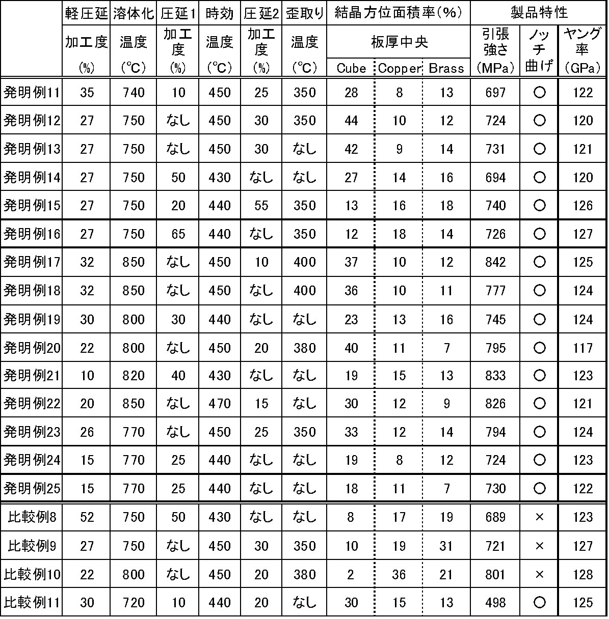
発明例は、いずれも本発明が規定する濃度のNiおよびSiを含有し、本発明が規定する条件で予備焼鈍および軽圧延を行ったものであり、板厚中央部の結晶方位が本発明の規定を満たし、ノッチ曲げが可能であり、650MPaを超える高い引張強さおよび110MPaを超える高いヤング率が得られた。ここで、圧延2の加工度が50%を超えた発明例15、および圧延1の加工度が60%を超えた発明例16では、ノッチ曲げ試験で割れが発生したものの、実用上許容できる極微細な割れであったため、○と評価した。
比較例8は軽圧延の加工度が50%を超えたものである。実施例1の合金と同様、板厚中央部の結晶方位が発明の規定から外れ、ノッチ曲げで割れが発生した。同じ成分の前記発明例15、16と比べると、引張強さが低いにも関わらず、発生した割れは電子部品としての機能を阻害するレベルの顕著なものであった。
比較例9、10は予備焼鈍での軟化度が本発明の規定を満足しなかったものである。実施例1の合金と同様、板厚中央部の結晶方位が発明の規定から外れ、ノッチ曲げで割れが発生した。
比較例11はNiおよびSi濃度が本発明の規定を下回ったものであり、ノッチ曲げ性は良好であったが、引張強さが500MPaにも達しなかった。
比較例8は軽圧延の加工度が50%を超えたものである。実施例1の合金と同様、板厚中央部の結晶方位が発明の規定から外れ、ノッチ曲げで割れが発生した。同じ成分の前記発明例15、16と比べると、引張強さが低いにも関わらず、発生した割れは電子部品としての機能を阻害するレベルの顕著なものであった。
比較例9、10は予備焼鈍での軟化度が本発明の規定を満足しなかったものである。実施例1の合金と同様、板厚中央部の結晶方位が発明の規定から外れ、ノッチ曲げで割れが発生した。
比較例11はNiおよびSi濃度が本発明の規定を下回ったものであり、ノッチ曲げ性は良好であったが、引張強さが500MPaにも達しなかった。
Claims (6)
- 0.8~4.5質量%のNi及び0.2~1.0質量%のSiを含有し、残部が銅及び不可避的不純物からなり、板厚に対し45~55%の断面位置である板厚方向の中央部において、板厚方向と平行にEBSD測定を行い、結晶方位を解析したときに、Cube方位{0 0 1}<1 0 0>の面積率が10~80%、Brass方位{1 1 0}<1 1 2>の面積率が20%以下、Copper方位{1 1 2}<1 1 1>の面積率が20%以下であるCu-Ni-Si系合金。
- Sn、Zn、Mg、Fe、Ti、Zr、Cr、Al、P、Mn、Co、Cr及びAgのうち1種以上を総量で0.005~3.0質量%含有する請求項1に記載のCu-Ni-Si系合金。
- 0.8~4.5質量%のNi及び0.2~1.0質量%のSiを含有し、残部が銅及び不可避的不純物からなるインゴットを作製し、前記インゴットを、温度800~1000℃で厚み5~20mmまで熱間圧延した後、加工度30~99%の冷間圧延を行い、軟化度0.25~0.75の熱処理を行って導電率を20~45%IACSの範囲に調整した後、加工度7~50%の冷間圧延を行い、次いで、700~900℃で5~300秒間の溶体化処理、及び、350~550℃で2~20時間の時効処理を行う方法であり、
前記軟化度は、温度Tのときの軟化度をSTとして、次式で示されるCu-Ni-Si系合金の製造方法:
ST=(σ0-σT)/(σ0-σ900)
(σ0は焼鈍前の引張強さであり、σTおよびσ900はそれぞれT℃および900℃で焼鈍後の引張強さである)。 - 前記インゴットがSn、Zn、Mg、Fe、Ti、Zr、Cr、Al、P、Mn、Co、Cr及びAgのうち1種以上を総量で0.005~3.0質量%含有する請求項3に記載のCu-Ni-Si系合金の製造方法。
- 請求項1又は2に記載の銅合金を備えた伸銅品。
- 請求項1又は2に記載の銅合金を備えた電子機器部品。
Priority Applications (2)
| Application Number | Priority Date | Filing Date | Title |
|---|---|---|---|
| CN201280012297.2A CN103403202B (zh) | 2011-03-09 | 2012-03-01 | Cu-Ni-Si系合金及其制造方法 |
| KR1020137026578A KR101808372B1 (ko) | 2011-03-09 | 2012-03-01 | Cu-Ni-Si 계 합금 및 그 제조 방법 |
Applications Claiming Priority (2)
| Application Number | Priority Date | Filing Date | Title |
|---|---|---|---|
| JP2011051975A JP4857395B1 (ja) | 2011-03-09 | 2011-03-09 | Cu−Ni−Si系合金及びその製造方法 |
| JP2011-051975 | 2011-03-09 |
Publications (1)
| Publication Number | Publication Date |
|---|---|
| WO2012121109A1 true WO2012121109A1 (ja) | 2012-09-13 |
Family
ID=45604520
Family Applications (1)
| Application Number | Title | Priority Date | Filing Date |
|---|---|---|---|
| PCT/JP2012/055255 Ceased WO2012121109A1 (ja) | 2011-03-09 | 2012-03-01 | Cu-Ni-Si系合金及びその製造方法 |
Country Status (5)
| Country | Link |
|---|---|
| JP (1) | JP4857395B1 (ja) |
| KR (1) | KR101808372B1 (ja) |
| CN (1) | CN103403202B (ja) |
| TW (1) | TWI447241B (ja) |
| WO (1) | WO2012121109A1 (ja) |
Families Citing this family (19)
| Publication number | Priority date | Publication date | Assignee | Title |
|---|---|---|---|---|
| JP5039862B1 (ja) * | 2011-07-15 | 2012-10-03 | Jx日鉱日石金属株式会社 | コルソン合金及びその製造方法 |
| KR101953412B1 (ko) * | 2011-08-05 | 2019-02-28 | 후루카와 덴키 고교 가부시키가이샤 | 이차전지 집전체용 압연 동박 및 그 제조방법 |
| JP5039863B1 (ja) * | 2011-10-21 | 2012-10-03 | Jx日鉱日石金属株式会社 | コルソン合金及びその製造方法 |
| JP5916418B2 (ja) * | 2012-02-13 | 2016-05-11 | 古河電気工業株式会社 | 銅合金板材およびその製造方法 |
| TWI461549B (zh) * | 2012-02-14 | 2014-11-21 | Jx日鑛日石金屬股份有限公司 | Carbene alloy and its manufacturing method |
| JP2016084542A (ja) * | 2012-03-26 | 2016-05-19 | Jx金属株式会社 | コルソン合金及びその製造方法 |
| JP6111028B2 (ja) * | 2012-03-26 | 2017-04-05 | Jx金属株式会社 | コルソン合金及びその製造方法 |
| JP6196757B2 (ja) * | 2012-07-12 | 2017-09-13 | Jx金属株式会社 | コルソン合金及びその製造方法 |
| JP6223057B2 (ja) | 2013-08-13 | 2017-11-01 | Jx金属株式会社 | 導電性及び曲げたわみ係数に優れる銅合金板 |
| CN103484719A (zh) * | 2013-09-29 | 2014-01-01 | 苏州市凯业金属制品有限公司 | 一种白铜合金金属管 |
| JP6050738B2 (ja) | 2013-11-25 | 2016-12-21 | Jx金属株式会社 | 導電性、成形加工性および応力緩和特性に優れる銅合金板 |
| JP6355671B2 (ja) * | 2016-03-31 | 2018-07-11 | Jx金属株式会社 | Cu−Ni−Si系銅合金条及びその製造方法 |
| JP2017014624A (ja) * | 2016-09-05 | 2017-01-19 | Jx金属株式会社 | コルソン合金及びその製造方法 |
| JP6440760B2 (ja) | 2017-03-21 | 2018-12-19 | Jx金属株式会社 | プレス加工後の寸法精度を改善した銅合金条 |
| JP6345290B1 (ja) | 2017-03-22 | 2018-06-20 | Jx金属株式会社 | プレス加工後の寸法精度を改善した銅合金条 |
| CN107326215A (zh) * | 2017-08-15 | 2017-11-07 | 徐高杰 | 一种槽楔用铜合金的加工方法 |
| JP6762333B2 (ja) * | 2018-03-26 | 2020-09-30 | Jx金属株式会社 | Cu−Ni−Si系銅合金条 |
| CN114752810B (zh) * | 2022-03-24 | 2023-04-11 | 江苏恒盈电子科技有限公司 | 一种线路板用高强度半导体引线框架及其制备方法 |
| CN114855026B (zh) * | 2022-03-25 | 2023-02-14 | 宁波博威合金材料股份有限公司 | 一种高性能析出强化型铜合金及其制备方法 |
Citations (5)
| Publication number | Priority date | Publication date | Assignee | Title |
|---|---|---|---|---|
| JP2006283059A (ja) * | 2005-03-31 | 2006-10-19 | Kobe Steel Ltd | 曲げ加工性に優れた高強度銅合金板及びその製造方法 |
| WO2009148101A1 (ja) * | 2008-06-03 | 2009-12-10 | 古河電気工業株式会社 | 銅合金板材およびその製造方法 |
| JP4563495B1 (ja) * | 2009-04-27 | 2010-10-13 | Dowaメタルテック株式会社 | 銅合金板材およびその製造方法 |
| JP2011012321A (ja) * | 2009-07-03 | 2011-01-20 | Furukawa Electric Co Ltd:The | 銅合金材およびその製造方法 |
| JP2011017072A (ja) * | 2009-07-10 | 2011-01-27 | Furukawa Electric Co Ltd:The | 銅合金材料 |
Family Cites Families (5)
| Publication number | Priority date | Publication date | Assignee | Title |
|---|---|---|---|---|
| JP4006460B1 (ja) * | 2006-05-26 | 2007-11-14 | 株式会社神戸製鋼所 | 高強度、高導電率および曲げ加工性に優れた銅合金およびその製造方法 |
| JP5085908B2 (ja) * | 2006-10-03 | 2012-11-28 | Jx日鉱日石金属株式会社 | 電子材料用銅合金及びその製造方法 |
| US20080190523A1 (en) * | 2007-02-13 | 2008-08-14 | Weilin Gao | Cu-Ni-Si-based copper alloy sheet material and method of manufacturing same |
| JP4596493B2 (ja) * | 2008-03-31 | 2010-12-08 | Jx日鉱日石金属株式会社 | 導電性ばね材に用いられるCu−Ni−Si系合金 |
| EP2610358A4 (en) | 2010-08-27 | 2017-05-03 | Furukawa Electric Co., Ltd. | Copper alloy sheet and manufacturing method for same |
-
2011
- 2011-03-09 JP JP2011051975A patent/JP4857395B1/ja active Active
-
2012
- 2012-03-01 KR KR1020137026578A patent/KR101808372B1/ko active Active
- 2012-03-01 CN CN201280012297.2A patent/CN103403202B/zh active Active
- 2012-03-01 WO PCT/JP2012/055255 patent/WO2012121109A1/ja not_active Ceased
- 2012-03-01 TW TW101106626A patent/TWI447241B/zh active
Patent Citations (5)
| Publication number | Priority date | Publication date | Assignee | Title |
|---|---|---|---|---|
| JP2006283059A (ja) * | 2005-03-31 | 2006-10-19 | Kobe Steel Ltd | 曲げ加工性に優れた高強度銅合金板及びその製造方法 |
| WO2009148101A1 (ja) * | 2008-06-03 | 2009-12-10 | 古河電気工業株式会社 | 銅合金板材およびその製造方法 |
| JP4563495B1 (ja) * | 2009-04-27 | 2010-10-13 | Dowaメタルテック株式会社 | 銅合金板材およびその製造方法 |
| JP2011012321A (ja) * | 2009-07-03 | 2011-01-20 | Furukawa Electric Co Ltd:The | 銅合金材およびその製造方法 |
| JP2011017072A (ja) * | 2009-07-10 | 2011-01-27 | Furukawa Electric Co Ltd:The | 銅合金材料 |
Also Published As
| Publication number | Publication date |
|---|---|
| CN103403202A (zh) | 2013-11-20 |
| KR20130143647A (ko) | 2013-12-31 |
| TW201239107A (en) | 2012-10-01 |
| TWI447241B (zh) | 2014-08-01 |
| JP4857395B1 (ja) | 2012-01-18 |
| JP2012188689A (ja) | 2012-10-04 |
| CN103403202B (zh) | 2016-08-10 |
| KR101808372B1 (ko) | 2017-12-12 |
Similar Documents
| Publication | Publication Date | Title |
|---|---|---|
| JP4857395B1 (ja) | Cu−Ni−Si系合金及びその製造方法 | |
| JP5117604B1 (ja) | Cu−Ni−Si系合金及びその製造方法 | |
| JP6228725B2 (ja) | Cu−Co−Si系合金及びその製造方法 | |
| JP2013104082A (ja) | Cu−Co−Si系合金及びその製造方法 | |
| JP2013100586A (ja) | チタン銅及びその製造方法 | |
| JP2016199808A (ja) | Cu−Co−Si系合金及びその製造方法 | |
| WO2013069376A1 (ja) | Cu-Co-Si系合金及びその製造方法 | |
| JP5039863B1 (ja) | コルソン合金及びその製造方法 | |
| JP6196757B2 (ja) | コルソン合金及びその製造方法 | |
| JP6111028B2 (ja) | コルソン合金及びその製造方法 | |
| JP6345290B1 (ja) | プレス加工後の寸法精度を改善した銅合金条 | |
| JP4987155B1 (ja) | Cu−Ni−Si系合金及びその製造方法 | |
| JP6246454B2 (ja) | Cu−Ni−Si系合金及びその製造方法 | |
| JP2016211078A (ja) | Cu−Ni−Si系合金及びその製造方法 | |
| JP2017014624A (ja) | コルソン合金及びその製造方法 |
Legal Events
| Date | Code | Title | Description |
|---|---|---|---|
| 121 | Ep: the epo has been informed by wipo that ep was designated in this application |
Ref document number: 12754576 Country of ref document: EP Kind code of ref document: A1 |
|
| NENP | Non-entry into the national phase |
Ref country code: DE |
|
| ENP | Entry into the national phase |
Ref document number: 20137026578 Country of ref document: KR Kind code of ref document: A |
|
| 122 | Ep: pct application non-entry in european phase |
Ref document number: 12754576 Country of ref document: EP Kind code of ref document: A1 |