WO2012115039A1 - 放射線画像検出装置及び放射線撮影装置 - Google Patents
放射線画像検出装置及び放射線撮影装置 Download PDFInfo
- Publication number
- WO2012115039A1 WO2012115039A1 PCT/JP2012/053970 JP2012053970W WO2012115039A1 WO 2012115039 A1 WO2012115039 A1 WO 2012115039A1 JP 2012053970 W JP2012053970 W JP 2012053970W WO 2012115039 A1 WO2012115039 A1 WO 2012115039A1
- Authority
- WO
- WIPO (PCT)
- Prior art keywords
- image detection
- sensor panel
- radiation
- detection apparatus
- radiation image
- Prior art date
- Legal status (The legal status is an assumption and is not a legal conclusion. Google has not performed a legal analysis and makes no representation as to the accuracy of the status listed.)
- Ceased
Links
Images










Classifications
-
- G—PHYSICS
- G01—MEASURING; TESTING
- G01T—MEASUREMENT OF NUCLEAR OR X-RADIATION
- G01T1/00—Measuring X-radiation, gamma radiation, corpuscular radiation, or cosmic radiation
- G01T1/16—Measuring radiation intensity
- G01T1/20—Measuring radiation intensity with scintillation detectors
- G01T1/202—Measuring radiation intensity with scintillation detectors the detector being a crystal
-
- A—HUMAN NECESSITIES
- A61—MEDICAL OR VETERINARY SCIENCE; HYGIENE
- A61B—DIAGNOSIS; SURGERY; IDENTIFICATION
- A61B6/00—Apparatus or devices for radiation diagnosis; Apparatus or devices for radiation diagnosis combined with radiation therapy equipment
- A61B6/42—Arrangements for detecting radiation specially adapted for radiation diagnosis
- A61B6/4208—Arrangements for detecting radiation specially adapted for radiation diagnosis characterised by using a particular type of detector
- A61B6/4216—Arrangements for detecting radiation specially adapted for radiation diagnosis characterised by using a particular type of detector using storage phosphor screens
-
- A—HUMAN NECESSITIES
- A61—MEDICAL OR VETERINARY SCIENCE; HYGIENE
- A61B—DIAGNOSIS; SURGERY; IDENTIFICATION
- A61B6/00—Apparatus or devices for radiation diagnosis; Apparatus or devices for radiation diagnosis combined with radiation therapy equipment
- A61B6/44—Constructional features of apparatus for radiation diagnosis
- A61B6/4429—Constructional features of apparatus for radiation diagnosis related to the mounting of source units and detector units
- A61B6/4464—Constructional features of apparatus for radiation diagnosis related to the mounting of source units and detector units the source unit or the detector unit being mounted to ceiling
Definitions
- the present invention relates to a radiation image detection apparatus and a radiation imaging apparatus.
- the indirect conversion type radiation image detection apparatus includes a scintillator formed of a fluorescent material such as CsI or NaI which emits fluorescence by radiation exposure, and a sensor panel having a two-dimensional array of photoelectric conversion elements.
- the radiation transmitted through the subject is once converted to light by the scintillator, and the fluorescence of the scintillator is photoelectrically converted by the group of photoelectric conversion elements of the sensor panel, whereby an electrical signal (digital image data) is generated.
- a technique of forming a scintillator by a group of columnar crystals of a fluorescent substance such as CsI is also known (see, for example, Patent Document 2).
- Columnar crystals are typically formed by growing crystals of a fluorescent substance in the form of columns on a support by vapor deposition.
- a support a sensor panel or an appropriate substrate is used.
- the sensor panel is a support
- a group of columnar crystals is directly formed on the sensor panel.
- a suitable substrate is used as a support, a group of columnar crystals formed on the substrate is bonded to the sensor panel.
- the columnar crystals formed by the vapor deposition method do not contain impurities such as a binder and have a light guiding effect to guide the fluorescence generated there in the crystal growth direction, thereby suppressing the diffusion of the fluorescence. Do. As a result, the sensitivity of the radiation image detecting apparatus can be improved, and the image sharpness can be improved.
- each columnar crystal grows substantially perpendicular to the surface of the support, and when the sensor panel is used as a support, it is a matter of course that each columnar crystal is also bonded to the sensor panel with a group of columnar crystals formed on the substrate. Are provided substantially perpendicular to the surface of the sensor panel.
- the angle of incidence on the columnar crystals provided perpendicular to the surface of the sensor panel increases as the radiation is deviated from the center of the irradiation field. Therefore, it progresses across a plurality of columnar crystals, resulting in a decrease in image sharpness.
- the radiation image detection apparatus described in patent document 2 is using the flexible sensor panel, and the sensor panel is curved so that each columnar crystal becomes parallel with respect to the radiation which spreads radially. In each part of the radiation field, each columnar crystal becomes parallel to the radiation, and a reduction in the image sharpness is prevented.
- the radiation image detection apparatus described in Patent Document 2 is a so-called back side scanning type (PS: Penetration Side Sampling) radiation image detection apparatus in which radiation is incident from the scintillator side.
- PSS Penetration Side Sampling
- the gap between the tips of the group of columnar crystals narrows and adjacent columnar crystals There is a risk that the tips of the two may come in contact with each other and be damaged.
- the radius of curvature at the time of bending the sensor panel is limited, and when the imaging distance (SID: Source-Image Distance) is relatively short, the columnar crystals can not be arranged in parallel to the radiation, and the image The sharpness of the image can not be obtained sufficiently.
- SID Source-Image Distance
- the present invention has been made in view of the above-described problems, and it is an object of the present invention to prevent damage to a phosphor when curving a sensor panel of a radiation image detection apparatus to improve the sharpness of an image.
- a radiation image detection apparatus comprising: a phosphor containing a fluorescent material that emits fluorescence upon exposure to radiation; and a sensor panel provided closely with the phosphor and detecting fluorescence emitted by the phosphor.
- the phosphor includes a columnar portion formed of an aggregate of columnar crystals formed by growing crystals of the phosphor in a columnar shape, and a radiation incident surface is provided on the opposite side of the sensor panel to the phosphor.
- the sensor panel is flexible, The radiation image detection apparatus curved so that the curvature center may be located in the said radiation
- the phosphor is disposed on the outer diameter side thereof, and the tip of the aggregate of columnar crystals forming the phosphor
- the gap between the parts is enlarged. Therefore, the contact between the tip portions of adjacent columnar crystals is avoided, and damage to the columnar crystals is prevented.
- each columnar crystal can be disposed parallel to the radiation in accordance with the imaging distance, and the sharpness of the image can be improved.
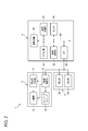
- FIG. 1 It is a figure which shows the structure of an example of a radiographic image detection apparatus and a radiography apparatus for describing embodiment of this invention. It is a figure which shows the control block of the radiography apparatus of FIG. It is a figure which shows the structure of the detection part of a radiographic image detection apparatus for describing embodiment of this invention. It is a figure which shows the structure of the sensor panel of the detection part of FIG. It is a figure which shows the structure of the fluorescent substance of the detection part of FIG. It is a figure which shows the VI-VI line cross section of the fluorescent substance of FIG. It is a figure which shows the VII-VII line cross section of the fluorescent substance of FIG. It is a figure which shows an example of the manufacturing method of the detection part of FIG.
- FIG. 1 shows an exemplary configuration of a radiation image detection apparatus and a radiation imaging apparatus for explaining an embodiment of the present invention
- FIG. 2 shows a control block of the radiation imaging apparatus of FIG.
- the X-ray imaging apparatus 1 is an X-ray diagnostic apparatus for imaging a subject (patient) H in a standing position, and is disposed opposite to the X-ray source 2 for emitting a cone beam X-ray to the subject H X-ray image detection apparatus 3 which detects X-rays transmitted through the object H from the X-ray source 2 and generates image data, and the exposure operation of the X-ray source 2 and X-ray image based on the operation of the operator It is roughly divided into a console 4 that controls the imaging operation of the detection device 3 and processes the image data acquired by the X-ray image detection device 3.
- the X-ray source 2 is held by an X-ray source holder 5 suspended from a ceiling.
- the X-ray image detection device 3 is held by a stand 6 installed on the floor.
- the X-ray source 2 is emitted from the X-ray tube 12 which generates X-rays in accordance with the high voltage applied from the high voltage generator 11 under the control of the X-ray source control unit 10 and the X-ray tube 12
- a collimator unit 14 having a movable collimator 13 for limiting an irradiation field so as to shield a portion which does not contribute to the inspection area of the subject H among X-rays.
- the X-ray tube 12 is an anode rotating type, emits an electron beam from a filament (not shown) as an electron emission source (cathode), and collides with the rotating anode 15 rotating at a predetermined speed. Generate. The collision part of the electron beam of the rotating anode 15 is the X-ray focal point 16.
- the X-ray source holding device 5 is connected to a carriage unit 21 configured to be movable in the horizontal direction (z direction) along the ceiling rail 20 installed on the ceiling, and extends downward from the carriage unit 21 A plurality of support portions 22, a drive mechanism for moving the carriage portion 21 along the ceiling rail, and a drive mechanism for extending and retracting the support portions 22 are provided.
- the X-ray source 2 is attached to the tip of the support 22.
- the X-ray source holding device 5 is provided with a position sensor (not shown) such as a potentiometer that detects the position of the X-ray source 2 in the horizontal direction by measuring the amount of movement of the carriage 21 along the ceiling rail. It is done.
- the detection value of the position sensor is supplied to the console 4 by wired or wireless communication.
- the stand 6 is provided with a main body 30 installed on the floor, a holding portion 31 attached to the main body 30 so as to be movable in the vertical direction, and a drive mechanism for moving the holding portion 31 up and down.
- the X-ray image detection device 3 is attached to the holding unit 31.
- the drive mechanism is controlled by the control device 40 of the console 4 described later based on the setting operation of the operator.
- the stand 6 is provided with a position sensor (not shown) such as a potentiometer that detects the position of the X-ray image detection device 3 in the vertical direction by measuring the amount of movement of the holding unit 31.
- the detection value of the position sensor is supplied to the console 4 by wired or wireless communication.
- the console 4 is provided with a control device 40 including a CPU, a ROM, a RAM, and the like.
- the control device 40 includes an input device 41 through which an operator inputs an imaging instruction and the content of the instruction, and an image processing unit 42 that processes the image data acquired by the X-ray image detection device 3 to generate an X-ray image.
- An image storage unit 43 for storing an X-ray image, a monitor 44 for displaying an X-ray image and the like, and an interface (I / F) 45 connected to each unit of the X-ray imaging apparatus 1 are provided.
- the control device 40, the input device 41, the image processing unit 42, the storage unit 43, the monitor 44, and the I / F 45 are connected via the bus 46.
- the controller 40 moves the X-ray source 2 to a position where the above-mentioned input imaging distance SID is to be obtained, based on the horizontal position of the X-ray source 2 supplied from the X-ray source holder 5.
- the radiation source holding device 5 is driven.
- the control device 40 moves the X-ray source 2 to the vertical position facing the X-ray image detection device 3 based on the vertical position of the X image detection device 3 supplied from the stand 6.
- the source holding device 5 is driven.
- the X-ray image detection apparatus 3 has a two-dimensional array of a scintillator (phosphor) 60 containing a fluorescent material that emits fluorescence by X-ray exposure and a photoelectric conversion element 70 that photoelectrically converts the fluorescence emitted by the scintillator 60. And have.
- the scintillator 60 is in close contact with the sensor panel 61 via a resin layer that optically couples the scintillator 60 and the group of photoelectric conversion elements 70.
- the detection unit 62 in which the scintillator 60 is in close contact with the sensor panel 61 is supported by the support 63 and accommodated in the housing 64.
- the detection unit 62 will be described below.
- FIG. 3 schematically shows the configuration of the detection unit 62
- FIG. 4 schematically shows the configuration of the sensor panel 61 of the detection unit 62. As shown in FIG. 3
- the detection unit 62 is a so-called ISS type, and in the sensor panel 61 to which the scintillator 60 is bonded, the sensor panel 61 is disposed on the X-ray source 2 side.
- the X-rays pass through the sensor panel 61 and enter the scintillator 60. Fluorescence is generated in the scintillator 60 to which the X-ray has entered, and the generated fluorescence is photoelectrically converted by the group of photoelectric conversion elements 70 of the sensor panel 61.
- the radiation incident side of the scintillator 60 that generates a large amount of fluorescence is provided adjacent to the sensor panel 61, so the sensitivity is improved.
- the sensor panel 61 has a flexible TFT substrate 72 in which a switch element 71 formed of thin film transistors (TFT: Thin Film Transistor) is formed on an insulating flexible substrate, and the group of photoelectric conversion elements 70 is the flexible TFT substrate 72. It is formed on top.
- a flat layer 75 is formed on the flexible TFT substrate 72 to cover the group of the photoelectric conversion elements 70 and to flatten the surface of the flexible TFT substrate 72.
- the planarization layer 75 is included in the above-described resin layer that optically couples the scintillator 60 and the group of photoelectric conversion elements 70.
- a resin such as polyimide or parylene can be used, and it is preferable to use a polyimide having a good film forming property.
- the thickness of the resin layer is preferably 50 ⁇ m or less, and more preferably 5 ⁇ m to 30 ⁇ m, from the viewpoints of sensitivity and image sharpness.
- the photoelectric conversion element 70 is configured of a photoconductive layer 73 generating charges when the fluorescence of the scintillator 60 is incident, and a pair of electrodes provided on the front and back surfaces of the photoconductive layer 73.
- An electrode 74a provided on the surface of the photoconductive layer 73 on the scintillator 60 side is a bias electrode for applying a bias voltage to the photoconductive layer 73, and an electrode 74b provided on the opposite surface is a photoconductive layer.
- a charge collection electrode for collecting the charge generated at 73.
- the switch elements 71 are two-dimensionally arranged on the flexible TFT substrate 72 corresponding to the two-dimensional arrangement of the photoelectric conversion elements 70, and the charge collection electrodes 74b of each photoelectric conversion element 70 are connected to the corresponding switch elements 71. ing. The charge collected by the charge collection electrode 74 b is read out via the switch element 71.
- the flexible TFT substrate 72 extends in one direction (row direction) and extends in a direction (column direction) orthogonal to the gate lines 76 with a plurality of gate lines 76 for turning on / off each switch element. And a plurality of signal lines 77 for reading out the charges via the switch element 71 in the on state. Further, connection terminals 78 to which the respective gate lines 76 and the respective signal lines 77 are connected are arranged at the periphery of the flexible TFT substrate 72. The connection terminal 78 is connected to a circuit board (not shown) via a connection circuit 79. This circuit board has a gate driver as an external circuit and a signal processing unit.
- the switch elements 71 are sequentially turned on row by row by a signal supplied from the gate driver via the gate line 76. Then, the charge read by the switch element 71 turned on is transmitted through the signal line 77 and input to the signal processing unit. As a result, the charges are sequentially read out in units of rows, and are converted into electric signals in the above-described signal processing unit to generate digital image data.
- FIG. 5 schematically shows the structure of the scintillator 60. As shown in FIG. 5
- CsI: Tl (thallium activated cesium iodide), NaI: Tl (thallium activated sodium iodide), CsI: Na (sodium activated cesium iodide), etc. may be used as the fluorescent material forming the scintillator 60.
- CsI: Tl is preferred in that the emission spectrum is matched with the maximum value (approximately 550 nm) of the spectral sensitivity of the a-Si photodiode.
- the scintillator 60 is composed of a columnar section 80 and a non-columnar section 81 provided on the sensor panel side of the columnar section 80.
- the columnar portion 80 and the non-columnar portion 81 are formed continuously in layers, and can be formed by a vapor deposition method as described in detail later.
- the scintillator 60 brings the non-columnar portion 81 into close contact with the sensor panel 61.
- the columnar portion 80 is formed of a group of columnar crystals 82 formed by growing crystals of the above-mentioned fluorescent substance in a columnar shape.
- Each columnar crystal 82 is provided substantially perpendicularly to the surface of the sensor panel 61. And, a gap is placed between the adjacent columnar crystals 82, and the respective columnar crystals 82 exist independently of each other.
- the non-columnar portion 81 is formed of a group of crystals in which crystals of the fluorescent material are relatively small. In the non-columnar portion 81 formed by a group of relatively small diameter crystals, the crystals are irregularly combined or overlap with each other, so that it is difficult to form a clear gap between the crystals.
- the non-columnar portion 81 may contain an amorphous body of the above-mentioned fluorescent substance.
- Diffusion of fluorescence generated in each columnar crystal 82 is suppressed by repeating total reflection in the columnar crystal 82 due to a difference in refractive index between the columnar crystal 82 and a gap (air) around the columnar crystal 82, and the columnar crystal 82 Are guided to the opposing photoelectric conversion element 70. Thereby, the sharpness of the image is improved.
- the non-columnar portion 81 formed of a relatively small diameter crystal or an aggregate thereof is denser than the columnar portion 80 and has a small porosity.
- the close contact between the scintillator 60 and the sensor panel 61 is improved by the scintillator 60 bringing the non-columnar portion 81 into close contact with the sensor panel 61. Thereby, the scintillator 60 is prevented from peeling off from the sensor panel 61.
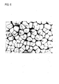
- FIG. 6 is an electron micrograph showing a cross section VI-VI in FIG. 5 of the scintillator 60.
- the columnar crystals 82 exhibit a substantially uniform cross-sectional diameter in the crystal growth direction, and have gaps around the columnar crystals 82, and the columnar crystals 82 It can be seen that they exist independently.
- the crystal diameter (column diameter) of the columnar crystal 82 is preferably 2 ⁇ m or more and 8 ⁇ m or less from the viewpoint of light guide effect, mechanical strength, and prevention of pixel defects. If the crystal diameter is too small, the mechanical strength of the columnar crystals 82 may be insufficient, and there is a concern that the columnar crystals 82 may be damaged due to impact etc. If the crystal diameter is too large, the number of columnar crystals 82 for each photoelectric conversion element 70 decreases. There is a concern that the probability of the element becoming a defect increases when a crack occurs.
- the column diameter indicates the maximum diameter of the crystal observed from the top surface of the columnar crystal 82 in the growth direction.
- the diameter of a column is measured by observing the top of the growth direction of the columnar crystal 82 with an SEM (scanning electron microscope). The observation is made at a magnification (about 2000 times) at which 100 to 200 columnar crystals 82 can be observed, and the maximum value of the column diameter is measured and averaged for all the crystals included in one shot.
- Column diameter ( ⁇ m) shall be read to two places after the decimal point, and the average value shall be the value obtained by rounding the second place after the decimal point according to JIS Z 8401.
- the thickness of the columnar portion 80 is preferably 200 ⁇ m or more and 700 ⁇ m or less from the viewpoint of sufficient radiation absorption in the columnar portion 80 and the sharpness of the image although it depends on the energy of radiation. If the thickness of the columnar section 80 is too small, radiation can not be absorbed sufficiently, and the sensitivity may be reduced. If the thickness is too large, light diffusion occurs, and the image is sharpened even by the light guiding effect of the columnar crystal. There is a concern that the degree will decline.
- FIG. 7 is an electron micrograph showing a VII-VII cross section in FIG. 5 of the scintillator 60.
- the non-columnar portion 81 crystal clear bonds occur irregularly and overlap between crystals, and a clear gap between crystals is not recognized as in the columnar portion 80.
- the diameter of the crystal forming the non-columnar portion 81 is preferably 7.0 ⁇ m or less from the viewpoint of adhesion. If the crystal diameter is too large, the flatness may be reduced and the adhesion to the sensor panel 61 may be reduced.
- a line connecting depressions (concave) generated between adjacent crystals is regarded as a boundary between the crystals, and the bonded crystals are regarded as the minimum polygon.
- the crystal grains were separated to measure the diameter of the column and the diameter of the crystal corresponding to the diameter of the column, and the average value was taken in the same manner as the diameter of the crystal in the columnar part 80, and the value was adopted.
- the thickness of the non-columnar portion 81 is preferably 5 ⁇ m or more and 50 ⁇ m or less from the viewpoint of adhesion to the sensor panel 61 and image quality. If the thickness of the non-columnar portion 81 is too small, sufficient adhesion with the sensor panel 61 may not be obtained. If the thickness is too large, the contribution of fluorescence in the non-columnar portion 81 and the non-columnar portion 81 There is a concern that the diffusion of the fluorescence of the image may increase and the sharpness of the image may decrease.
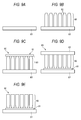
- FIG. 8 schematically shows an example of a method of manufacturing the scintillator 60.
- the method of manufacturing the scintillator 60 shown in FIG. 8 is to form the scintillator 60 directly on the surface of the sensor panel 61 by vapor deposition. According to the vapor deposition method, the columnar portion 80 and the non-columnar portion 81 can be continuously and integrally formed. Below, the case where CsI: Tl is used as a fluorescent substance is demonstrated to an example.
- the scintillator 60 is formed by vapor deposition, for example, by heating CsI: Tl in a resistance heating crucible under the environment of a vacuum degree of 0.01 to 10 Pa by heating or vaporizing the temperature of the sensor panel 61.
- CsI: Tl is deposited on the sensor panel 61 with room temperature (20.degree. C.) to 300.degree.
- the scintillator 60 is formed on the sensor panel 61 in a state of being in close contact with the sensor panel 61 in the non-columnar portion 81, and the detection unit 62 is configured.
- FIG. 9 schematically shows another example of the method of manufacturing the scintillator 60.
- the method of manufacturing the scintillator 60 shown in FIG. 9 uses the substrate 83, forms the scintillator 60 on the surface of the substrate 83, and then bonds the scintillator 60 formed on the substrate 83 to the sensor panel 61.
- a carbon plate, carbon fiber reinforced plastic (CFRP), a glass plate, a quartz substrate, a sapphire substrate, a metal sheet such as iron, tin, chromium or aluminum, or the like can be used. As long as it can form, it is not limited to the above-mentioned thing.
- the formation of the scintillator 60 is by vapor deposition.
- CsI Tl is vaporized by heating in a resistance heating type crucible or the like in a vacuum degree of 0.01 to 10 Pa, and the temperature of the support 11 is set to room temperature (20 ° C.) to 300 ° C. Tl is deposited on the substrate 83.
- the adhesive layer is not particularly limited as long as it can reach the sensor panel 61 without attenuating the fluorescence of the scintillator 60.
- a UV curing adhesive, a heat curing adhesive, a room temperature curing adhesive, or hot Adhesives such as melt-type adhesives, or rubber-based pressure-sensitive adhesives, silicone-based pressure-sensitive adhesives, acrylic-based pressure-sensitive adhesives, etc., or double-sided adhesive / pressure-sensitive adhesive sheets provided with these adhesives and pressure-sensitive adhesives on both sides
- the adhesive it is preferable to use an adhesive made of a low viscosity epoxy resin capable of forming an adhesive layer sufficiently thin with respect to the element size from the viewpoint of not reducing the sharpness of the image.
- the pressure-sensitive adhesive an acrylic pressure-sensitive adhesive which is less deteriorated by light or oxidation is preferable.
- the adhesive layer is included in the above-described resin layer that optically couples the scintillator 60 and the group of photoelectric conversion elements 70 of the sensor panel 61. .
- the X-ray image detection device 3 further includes a bending portion 65 for bending the detection portion 62 configured as described above.
- the bending portion 65 will be described.
- FIG. 10 and 11 show the configuration of the bending portion 65.
- FIG. 10 and 11 show the configuration of the bending portion 65.
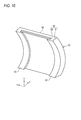
- the curved portion 65 is a support 63 for supporting the detection portion 62, a driven member 90 provided on the support 63, which is curved in response to a physical stimulation, and the above-mentioned physical stimulation on the driven member 90. And a drive unit 91 for providing the same.
- the support 63 has a light shielding property, and a cover 92 that covers the scintillator 60 side of the detection unit 62, that is, the side opposite to the X-ray incident side, and a pair of sides of the detection unit 62 (in the illustrated example, y And a locking portion 93 for locking a pair of sides along the direction.
- the support 63 is formed of a material having a degree of flexibility capable of self-supporting, and, for example, rubber, pitch-based carbon fiber, and the like can be suitably used.
- a belt-shaped bimetal 90 which is curved by heat as a physical stimulus is used as the driven member 90.
- a plurality of bimetals 90 are attached in parallel to the back surface of the cover portion 92, and these bimetals 90 extend in the y direction in parallel with each other, and are provided at appropriate intervals in the x direction.
- the drive unit 91 applies an appropriate current to each bimetal 90.
- the bimetal 90 to which the current is applied from the drive unit 91 is curved so that the center of curvature is located on the X-ray incident side in the detection unit 62 due to self-heating due to its resistance.
- the drive unit 91 is configured to apply a current to each bimetal 90 according to the imaging distance SID set in the console 4, and the bimetal 90 to which the current is applied from the drive unit 91 is an X-ray. It is curved so as to substantially follow a cylindrical surface centered on a straight line parallel to the x direction passing through the focal point 16.
- the support 63 and the detection portion 62 supported thereby also bend.
- the detection unit 62 is also similarly curved, and the center of curvature thereof is X It is disposed at a position substantially coincident with the line focal point 16.
- FIG. 12 schematically illustrates the curved detection unit 62.
- each columnar crystal 82 of the scintillator 60 exists independently of each other with a gap therebetween. Also by the curvature of the sensor panel 61, each columnar crystal 82 expands and shrinks the gap around it to keep the surface perpendicular to the surface of the sensor panel 61.
- the sensor panel 61 is curved along a substantially cylindrical surface having a straight line parallel to the x direction passing through the X-ray focal point 16 as a central axis. Therefore, each columnar crystal 82 is directed to the above-mentioned central axis and made substantially parallel to the X-ray incident thereon in plan view. As a result, X-rays are prevented from traveling in the scintillator 60 across the plurality of columnar crystals 82, and the sharpness of the image is improved.
- the scintillator 60 is positioned on the outer diameter side in the detection unit 62 which is curved so that the center of curvature is positioned on the X-ray incident surface side, and along with the above-described curvature of the detection unit 62
- the gap between the tips of the 82 groups is enlarged. Thereby, the contact between the tip portions of adjacent columnar crystals 82 is avoided, and damage to the columnar crystals 82 is prevented.
- the scintillator 60 is in close contact with the sensor panel 61 in the non-columnar portion 81 whose porosity is smaller than that of the columnar portion 80, and the adhesion thereof is enhanced. This prevents the scintillator 60 from peeling off due to the curvature of the sensor panel 61.
- the exposed detection unit 62 (scintillator 60 and sensor panel 61) is directly supported by the support 63 and bent, and the support 63 covers the detection unit 62.
- the support 63 covers the detection unit 62.
- a control including a circuit board having a gate driver and a signal processing unit as an external circuit electrically connected with the gate line 76 (see FIG. 4) and the signal line 77 (see FIG. 4)
- the unit 101 is provided along one side of the detection unit 62.
- a hard IC typically formed of an inorganic semiconductor material such as silicon is used for the gate driver and the signal processing unit, and it is difficult to bend the entire control unit that accommodates these.
- the detection unit in which the control unit 101 is juxtaposed to the support body 63 curved substantially along a cylindrical surface whose central axis is a straight line parallel to the x direction passing through the X-ray focal point 16
- One side of 62 may be disposed in parallel with the x direction, and only the detection unit 62 may be supported by the support 63, and only the detection unit 62 may be curved.
- the gate driver circuit instead of a hard IC formed of an inorganic semiconductor material, the gate driver circuit can be formed of a flexible organic TFT. Therefore, as shown in FIG. 14, a gate driver circuit 102 made of an organic TFT may be provided on the flexible TFT substrate 72 of the sensor panel 61. In this case, the detection unit 62 is flexible because the gate driver circuit 102 is flexible. Is not disturbed.
- the temperature of the bimetal 90 for example using temperature control elements, such as a Peltier element. May be controlled.
- a shape memory alloy can also be used.
- FIG.15 and FIG.16 shows the modification of the X-ray-image detection apparatus 3 mentioned above.
- the cover part 92 of the support 63 supporting the detection part 62 is provided with one bimetal 90 formed so as to cover almost the entire area thereof.
- the bimetal 90 to which current is applied from the drive unit 91 according to the imaging distance SID set by the console 4 is curved along a spherical surface centered on the X-ray focal point 16.
- the support 63 and the detection unit 62 supported thereby also bend along a spherical surface centered on the X-ray focal point 16.
- each columnar crystal 82 points to the X-ray focal point 16 and is approximately parallel to the X-rays incident thereon.
- X-rays are prevented from traveling in the scintillator 60 across the plurality of columnar crystals 82, and the sharpness of the image is further improved.
- FIG. 17 shows a modification of the X-ray imaging apparatus 1 described above
- FIG. 18 shows a configuration of an X-ray image detection apparatus of the X-ray imaging apparatus of FIG.
- the X-ray imaging apparatus 201 has a plurality of X-ray sources 202.
- the X-ray source 202 sequentially emits X-rays under the control of the control device 40 of the console 4, and the X-ray focal point position moves sequentially as the X-ray source 202 is switched.
- the cover part 92 of the support 63 supporting the detection part 62 is divided into a plurality of areas, and the bimetal 90 is provided in each area.
- the bimetal 90 is provided in each area.
- three regions are divided in each of the x direction and the y direction, and a bimetal 90 is provided in each region.
- the drive unit 91 is configured to independently control the current applied to each bimetal 90 for each bimetal 90 according to the X-ray focal position.
- FIG. 19 schematically illustrates the curvature of the detection unit 62 in the X-ray image detection apparatus 203.
- the curvature radius of the detection unit 62 and the direction of the straight line connecting the center of the detection unit 62 and the center of curvature can be variously changed by applying a current controlled independently to each bimetal 90 from the drive unit 91 it can.
- the detection unit 62 when the applied current to the bimetal 90 in each region is equal, the detection unit 62 is curved substantially symmetrically with respect to the central portion of the detection unit 62. A straight line connecting the central portion of the detection portion 62 at that time and the center of curvature at the central portion is substantially along the z direction (FIG. 19A).
- the current applied to the bimetal 90 in the central row region in the y direction with respect to the current applied to the bimetal 90 in one of the row regions is increased and the current applied to the bimetal 90 in the other row region is increased.
- the detection unit 62 curves asymmetrically with respect to the center of the detection unit 62.
- the straight line connecting the center of the detection unit 62 and the center of curvature at that time is inclined with respect to the z direction (FIG. 19B, C).
- each columnar crystal 82 of the scintillator 60 can be made approximately parallel to the X-rays incident thereon with respect to radiation from different X-ray focal positions.
- FIG. 20 shows another modification of the X-ray image detection apparatus 3 described above.
- a driven member for bending the detection unit 62 an example using a bimetal or the like that is curved by heat as an external stimulus is described as a driven member for bending the detection unit 62.
- the driven member which can expand and contract can be used, and as such a driven member, for example, an artificial muscle or a piezo element utilizing volume phase transition of a polymer gel can be exemplified, and these can be obtained by an applied voltage as an external stimulus. Stretch.
- the outer peripheral portion of the support 63 that supports the detection unit 62 is fixed to the inner wall of the housing 64.
- An artificial muscle 390 is provided at the center of the cover 92 of the support 63.
- the drive unit (not shown) is configured to control the voltage applied to the artificial muscle 390 according to the imaging distance SID.
- the support 63 is curved along the spherical surface centered on the X-ray focal point 16 by the contraction of the artificial muscle 390 to which the voltage is applied from the drive unit 91 according to the imaging distance SID, and the support 63 is supported thereby.
- the detector 62 also curves along a spherical surface centered on the X-ray focal point 16. Thereby, each columnar crystal 82 points to the X-ray focal point 16 and is approximately parallel to the X-rays incident thereon.
- the central portion of the cover portion 92 of the support 63 is fixed to the housing 64, and the outer peripheral portion of the support 63 is supported by a plurality of artificial muscles 390, and the voltage applied to each artificial muscle 390 is artificially It can also be configured to control each muscle 390 independently.
- the X-ray source 202 is controlled by independently controlling the applied voltage to each artificial muscle 390 according to the X-ray focal position.
- the center of curvature of the detection unit 62 can be made to coincide with the X-ray focal point position which moves sequentially with the switching of.
- Each of the above-described radiation image detection devices can detect radiation images with high sensitivity and high resolution, and therefore it is required to detect sharp images with a low radiation dose, medical diagnostic X-ray imaging for mammography and the like
- the device can be incorporated into various devices and used. For example, it can be used for nondestructive inspection as an industrial X-ray imaging apparatus, or as a detection apparatus for particle beams (alpha ray, beta ray, gamma ray) other than electromagnetic waves, and its application range is wide. .
- Photoelectric conversion element For example, an inorganic semiconductor material such as amorphous silicon is often used as the photoconductive layer 73 (see FIG. 3) of the photoelectric conversion element 70 described above, but the organic photoelectric conversion described in, for example, JP2009-32854A. (OPC; Organic photoelectric conversion) materials can also be used. A film formed of this OPC material (hereinafter referred to as an OPC film) can be used as the photoconductive layer 73.
- the OPC film contains an organic photoelectric conversion material, absorbs light emitted from the phosphor layer, and generates a charge according to the absorbed light.
- the absorption peak wavelength of the organic photoelectric conversion material constituting the OPC film is closer to the emission peak wavelength of the phosphor layer in order to absorb the light emitted from the phosphor layer most efficiently.
- the absorption peak wavelength of the organic photoelectric conversion material matches the emission peak wavelength of the phosphor layer, but if the difference between the two is small, light emitted from the phosphor layer can be sufficiently absorbed. It is.
- the difference between the absorption peak wavelength of the organic photoelectric conversion material and the emission peak wavelength for radiation of the phosphor layer is preferably 10 nm or less, and more preferably 5 nm or less.
- organic photoelectric conversion material which can satisfy such conditions
- arylidene organic compounds, quinacridone organic compounds, and phthalocyanine organic compounds can be mentioned.
- the absorption peak wavelength of quinacridone in the visible region is 560 nm
- CsI (Tl) the material of the phosphor layer
- the difference between the above peak wavelengths should be 5 nm or less As a result, the amount of charge generated in the OPC film can be almost maximized.
- At least a part of the organic layer provided between the bias electrode 74a and the charge collection electrode 74b can be made of an OPC film. More specifically, the organic layer is a site that absorbs electromagnetic waves, a photoelectric conversion site, an electron transport site, a hole transport site, an electron blocking site, a hole blocking site, a crystallization prevention site, an electrode, and an interlayer contact improvement. It can be formed by stacking or mixing parts or the like.
- the organic layer preferably contains an organic p-type compound or an organic n-type compound.
- the organic p-type semiconductor (compound) is a donor type organic semiconductor (compound) mainly represented by a hole transporting organic compound, and refers to an organic compound having a property of easily giving an electron. More specifically, it refers to an organic compound having a smaller ionization potential when used in contact with two organic materials. Therefore, as the donor organic compound, any organic compound having an electron donating property can be used.
- the metal complex etc. which it has as can be used.
- the present invention is not limited to these, and any organic compound having a smaller ionization potential than the organic compound used as the n-type (acceptor property) compound can be used as the donor organic semiconductor.
- the organic n-type semiconductor is an acceptor-type organic semiconductor (compound) mainly represented by an electron transporting organic compound, and refers to an organic compound having a property of easily accepting an electron. More specifically, when the two organic compounds are brought into contact and used, the organic compound having the larger electron affinity is used. Therefore, as the acceptor type organic compound, any organic compound can be used as long as it is an electron-accepting organic compound.
- fused aromatic carbocyclic compounds naphthalene derivative, anthracene derivative, phenanthrene derivative, tetracene derivative, pyrene derivative, perylene derivative, fluoranthene derivative
- 5- to 7-membered heterocyclic compound containing nitrogen atom, oxygen atom, sulfur atom Eg pyridine, pyrazine, pyrimidine, pyridazine, triazine, quinoline, quinoxaline, quinazoline, quintaline, phthalazine, cinnoline, isoquinoline, pteridine, acridine, phenazine, phenanthroline, tetrazole, pyrazole, imidazole, thiazole, oxazole, indazole, benzimidazole, benzotriazole, Benzoxazole, benzothiazole, carbazole, purine, triazolopyridazine, triazolopyrim
- cyanine dyes can be used, but preferably, cyanine dyes, styryl dyes, hemicyanine dyes, merocyanine dyes (including zeromethine merocyanine (simple merocyanine)), trinuclear Merocyanine dyes, tetranuclear merocyanine dyes, rhodacyanine dyes, complex cyanine dyes, complex merocyanine dyes, allopolar dyes, oxonol dyes, hemioxonol dyes, squalium dyes, croconium dyes, azamethine dyes, coumarin dyes, arylidene dyes, anthraquinone dyes, triphenyl Methane dyes, azo dyes, azomethine dyes, spiro compounds, metallocene dyes, fluorenone dyes, fulgide dyes, per
- a p-type semiconductor layer and an n-type semiconductor layer are provided between a pair of electrodes, and at least one of the p-type semiconductor and the n-type semiconductor is an organic semiconductor, and between the semiconductor layers
- a photoelectric conversion film (photosensitive layer) having a bulk heterojunction structure layer including a p-type semiconductor and an n-type semiconductor as an intermediate layer can be suitably used.
- the bulk heterojunction structure layer in the photoelectric conversion film, it is possible to compensate for the short carrier diffusion length of the organic layer and to improve the photoelectric conversion efficiency.
- the bulk heterojunction structure is described in detail in Japanese Patent Application Laid-Open No. 2005-303266.
- the thickness of the photoelectric conversion film is preferably as large as possible from the viewpoint of absorbing light from the phosphor layer, but in consideration of the proportion not contributing to charge separation, it is preferably 30 nm to 300 nm, more preferably 50 nm to 250 nm. Or less, particularly preferably 80 nm or more and 200 nm or less.
- the description in JP-A-2009-32854 can be referred to.
- switch element Although an inorganic semiconductor material such as amorphous silicon is often used as the active layer of the switch element 71, for example, an organic material can be used as described in JP-A-2009-212389.
- the organic TFT may have any type of structure, but the most preferred is a field effect transistor (FET) structure.
- FET field effect transistor
- a gate electrode is provided on a part of the upper surface of the insulating substrate, and an insulator layer is provided so as to cover the electrode and to be in contact with the substrate at portions other than the electrode.
- a semiconductor active layer is provided on the upper surface of the insulator layer, and the transparent source electrode and the transparent drain electrode are disposed separately on a part of the upper surface.
- a top contact type device a bottom contact type device in which the source electrode and the drain electrode are under the semiconductor active layer can also be preferably used.
- a vertical transistor structure in which carriers flow in the film thickness direction of the organic semiconductor film may be used.
- the organic semiconductor material referred to here is an organic material exhibiting the characteristics of a semiconductor, and like a semiconductor made of an inorganic material, a p-type organic semiconductor material (or simply p-type) which conducts holes as a carrier Materials, also referred to as hole transport materials), and n-type organic semiconductor materials (or simply referred to as n-type materials or electron transport materials) that conduct electrons as carriers.
- p-type organic semiconductor materials or simply referred to as n-type materials or electron transport materials
- Many organic semiconductor materials generally exhibit better characteristics in the case of p-type materials, and since p-type transistors are generally superior in transistor operation stability under the atmosphere, here, p-type organic semiconductors are used here. The materials will be described.
- One of the characteristics of the organic thin film transistor is carrier mobility (also referred to simply as mobility) ⁇ which indicates the mobility of carriers in the organic semiconductor layer.
- the mobility can be high, preferably 1.0 ⁇ 10 ⁇ 7 cm 2 / Vs or higher, and more preferably 1.0 ⁇ 10 ⁇ 6 cm 2 / Vs or higher Preferably, it is more preferably 1.0 ⁇ 10 ⁇ 5 cm 2 / Vs or more.
- the mobility can be determined by characteristics when a field effect transistor (FET) element is manufactured or a time of flight measurement (TOF) method.
- FET field effect transistor
- TOF time of flight measurement
- the p-type organic semiconductor material may be a low molecular weight material or a high molecular weight material, but is preferably a low molecular weight material.
- the low molecular weight material can be easily purified because it can be applied to various purification methods such as sublimation purification, recrystallization, column chromatography, etc., and its molecular structure is fixed, so it is easy to take a crystal structure with high order, Many exhibit high characteristics for reasons such as
- the molecular weight of the low molecular weight material is preferably 100 or more and 5000 or less, more preferably 150 or more and 3000 or less, and still more preferably 200 or more and 2000 or less.
- a phthalocyanine compound or a naphthalocyanine compound can be exemplified, and specific examples are shown below.
- M represents a metal atom
- Bu represents a butyl group
- Pr represents a propyl group
- Et represents an ethyl group
- Ph represents a phenyl group.
- the material constituting the gate electrode, the source electrode, or the drain electrode is not particularly limited as long as it has the necessary conductivity, and for example, ITO (indium-doped tin oxide), IZO (indium-doped zinc oxide), Transparent conductive oxides such as SnO 2 , ATO (antimony-doped tin oxide), ZnO, AZO (aluminum-doped zinc oxide), GZO (gallium-doped zinc oxide), TiO 2 , FTO (fluorine-doped tin oxide), PEDOT / PSS
- transparent conductive polymers such as (poly (3,4-ethylenedioxythiophene) / polystyrene sulfonic acid) and carbon materials such as carbon nanotubes.
- These electrode materials can be formed into a film by methods, such as a vacuum evaporation method, sputtering, the solution application method, etc., for example.
- the material used for the insulating layer is not particularly limited as long as it has a necessary insulating effect, but, for example, inorganic materials such as silicon dioxide, silicon nitride, and alumina, polyester (PEN (polyethylene naphthalate), PET ( Examples include organic materials such as polyethylene terephthalate), polycarbonates, polyimides, polyamides, polyacrylates, epoxy resins, polyparaxylylene resins, novolac resins, PVA (polyvinyl alcohol), PS (polystyrene) and the like.
- These insulating film materials can be formed into a film by methods, such as a vacuum evaporation method, sputtering, the solution application method, etc., for example.
- the description of Japanese Patent Application Laid-Open No. 2009-212389 can be referred to.
- an amorphous oxide described in JP-A-2010-186860 can also be used.
- an active layer containing an amorphous oxide which the field effect transistor described in JP-A-2010-186860 has will be described.
- the active layer functions as a channel layer of a field effect transistor in which electrons or holes move.
- the active layer is configured to include an amorphous oxide semiconductor.
- the amorphous oxide semiconductor is preferably formed over a flexible substrate because it can be deposited at low temperature.
- the amorphous oxide semiconductor used for the active layer is preferably an amorphous oxide containing at least one element selected from the group consisting of In, Sn, Zn or Cd, more preferably In And an amorphous oxide containing at least one selected from the group consisting of Sn and Zn, more preferably an amorphous oxide containing at least one selected from the group consisting of In and Zn.
- amorphous oxide used in the active layer include In 2 O 3 , ZnO, SnO 2 , CdO, Indium-Zinc-Oxide (IZO), Indium-Tin-Oxide (ITO), and Gallium- Zinc-Oxide (GZO), Indium-Gallium-Oxide (IGO), Indium-Gallium-Zinc-Oxide (IGZO) may be mentioned.
- a film formation method of the active layer it is preferable to use a vapor phase film formation method with a polycrystalline sintered body of an oxide semiconductor as a target.
- vapor deposition methods sputtering and pulsed laser deposition (PLD) are suitable.
- PLD pulsed laser deposition
- film formation is performed by controlling the degree of vacuum and the flow rate of oxygen by RF magnetron sputtering deposition.
- the formed active layer is an amorphous film by a well-known X-ray diffraction method.
- the composition ratio of the active layer is determined by RBS (Rutherford backscattering) analysis.
- the electric conductivity of the active layer is preferably 10 -4 Scm -1 or more and 10 2 Scm -1 or more, more preferably 10 -1 Scm -1 or more and 10 2 Scm -1 or less.
- Examples of the method of adjusting the electrical conductivity of the active layer include a known method of adjusting with oxygen defects, a method of adjusting with the composition ratio, a method of adjusting with impurities, and a method of adjusting with an oxide semiconductor material.
- the description in JP-A-2010-186860 can be referred to.
- plastic films are mentioned as an insulating flexible substrate.
- plastic films include polyethylene terephthalate (PET), polyethylene naphthalate (PEN), polyethersulfone (PES), polyetherimide, polyetheretherketone, polyphenylene sulfide, polyarylate, polyimide, polycarbonate (PC), cellulose triacetate Examples include films made of (TAC), cellulose acetate propionate (CAP) and the like.
- these plastic films may contain an organic or inorganic filler.
- a flexible substrate formed using aramid, bio-nanofiber, or the like having characteristics that can not be obtained with existing glass or plastic, such as flexible, low thermal expansion, and high strength, can also be suitably used.
- the aramid material has high heat resistance with a glass transition temperature of 315 ° C., high rigidity with a Young's modulus of 10 GPa, and high dimensional stability with a thermal expansion coefficient of -3 to 5 ppm / ° C. For this reason, when a film made of aramid is used, high quality film formation of the semiconductor layer can be easily performed as compared with the case of using a general resin film. In addition, due to the high heat resistance of the aramid material, the electrode material can be cured at high temperature to reduce resistance. Furthermore, it is possible to cope with automatic mounting of an IC including a solder reflow process.
- the thermal expansion coefficient is close to that of ITO (indium tin oxide), gas barrier film, and glass substrate, warpage after manufacturing is small. And it is hard to break.
- a halogen-free (free from JPCA-ES01-2003) aramid material which does not contain a halogen from the viewpoint of environmental load reduction.
- the aramid film may be laminated with a glass substrate or a PET substrate, or may be attached to the housing of the device.
- an aramid material that is easy to form into a colorless, transparent, and thin film by solving the low solubility in a solvent by the height of cohesion (hydrogen bonding) between aramid molecules by molecular design. It can be used for Solubility is maintained while maintaining a highly linear rod-like molecular structure that leads to high rigidity and dimensional stability of the aramid material by controlling the order of the monomer unit and the molecular species design to control the substituent species and position on the aromatic ring. Good ease of molding is obtained. This molecular design can realize halogen-free.
- the aramid material by which the characteristic of the in-plane direction of a film was optimized.
- a rod-shaped molecular structure with high linearity and anisotropy in physical properties by controlling tension conditions for each step of solution casting, longitudinal stretching, and transverse stretching according to the strength of the aramid film which changes gradually during molding. It is possible to balance the in-plane characteristics of the aramid film which tends to occur.
- the solution casting step isotropicization of physical properties in the in-plane thickness direction by controlling the drying speed of the solvent, and optimization of the strength of the film containing the solvent and the peeling strength from the cast drum are achieved.
- the longitudinal stretching step the stretching conditions according to the strength of the film, which gradually changes during stretching, and the amount of residual solvent are precisely controlled.
- control of the conditions of transverse drawing according to the change in film strength which changes due to heating, and control of the conditions of transverse drawing for relieving the residual stress of the film are achieved.
- the use of such an aramid material can solve the problem of curling of the aramid film after molding.
- the rod-like molecular structure with high linearity unique to the aramid is maintained in any of the above-mentioned device for the ease of molding and the device for the balance of the characteristics in the film in-plane direction, so the thermal expansion coefficient can be maintained low. It is also possible to further reduce the thermal expansion coefficient by, for example, changing the stretching conditions at the time of film formation.
- Nanofibers can be used as a reinforcement for transparent and flexible resin materials, since components small enough to the wavelength of light do not cause light scattering.
- the cellulose microfibril bundle produced by bacteria acetate bacteria, Acetobacter Xylinum
- a transparent bio-nano nano that exhibits about 90% light transmittance at a wavelength of 500 nm while containing fibers at a high ratio of about 60 to 70% by impregnating and curing a transparent resin such as an acrylic resin or an epoxy resin in a bacterial cellulose sheet.
- a transparent resin such as an acrylic resin or an epoxy resin in a bacterial cellulose sheet.
- This bionanofiber provides a low coefficient of thermal expansion (about 3 to 7 ppm), comparable strength to steel (about 460 MPa), and high elasticity (about 30 GPa) comparable to silicon crystals.
- the configuration of the above-described bio-nanofiber can be referred to, for example, the description of Japanese Patent Application Publication No. 2008-34556.
- a radiation image detector comprising: a phosphor containing a fluorescent substance that emits fluorescence upon exposure to radiation; and a sensor panel provided closely with the phosphor and detecting fluorescence emitted by the phosphor.
- the phosphor includes a columnar portion formed of an aggregate of columnar crystals formed by growing crystals of the phosphor in a columnar shape, and a radiation incident surface is provided on the opposite side of the sensor panel to the phosphor.
- the sensor panel is flexible, The radiation image detection apparatus curved so that the curvature center may be located in the said radiation
- the radiation image detection apparatus further comprising: a bending portion that supports the sensor panel and bends the sensor panel variably in the position of the center of curvature.
- a bending portion that supports the sensor panel and bends the sensor panel variably in the position of the center of curvature.
- the bending section bends the sensor panel so as to change a radius of curvature of the sensor panel.
- the bending section bends the sensor panel in a variable direction of a straight line connecting the center of the sensor panel and the center of curvature. Detection device.
- the radiation image detecting apparatus according to any one of (2) to (4), wherein the bending portion is curved in response to a physical stimulus and at least one driven target attached to the sensor panel. Radiation image detection device including the body.
- the radiation image detection apparatus according to (5), wherein the driven body is a bimetal.
- the bending unit includes a drive unit that applies a current to the bimetal.
- the radiation image detecting apparatus according to any one of (2) to (4) above, wherein the bending portion expands and contracts in response to physical stimulation, one end is connected to the sensor panel, and the other end is A radiation image detecting apparatus comprising at least one fixed driven body.
- the phosphor further includes a non-columnar portion having a smaller porosity than the columnar portion, and the non-columnar portion A radiographic image detection device in close contact with the sensor panel; (13) The radiation image detecting apparatus according to the above (12), wherein the non-columnar portion has a thickness of 5 ⁇ m to 50 ⁇ m.
- a radiation image detection device according to any one of (1) to (13), and a radiation source for emitting radiation toward the radiation image detection device, the center of curvature of the sensor panel being the A radiograph that is in line with the radiation focus.
- the radiation image detecting device according to any one of (2) to (9) above, a radiation source for emitting radiation toward the radiation image detecting device, and the relative position of the radiation source with respect to the radiation image detecting device And the bending section bends the sensor panel such that the position of the center of curvature of the sensor panel changes in accordance with the relative position of the radiation source detected by the detecting section. Radiography equipment.
- the phosphor is disposed on the outer diameter side thereof, and the tip of the aggregate of columnar crystals forming the phosphor
- the gap between the parts is enlarged. Therefore, the contact between the tip portions of adjacent columnar crystals is avoided, and damage to the columnar crystals is prevented.
- each columnar crystal can be disposed parallel to the radiation in accordance with the imaging distance, and the sharpness of the image can be improved.
- Reference Signs List 1 X-ray imaging system 2 X-ray source 3 X-ray image detection device 4 console 5 X-ray source holding device 6 stand 10 X-ray source control unit 11 high voltage generator 12 X-ray tube 13 collimator 14 collimator unit 15 collimator unit 15 rotating anode 16 X Line Focus 20 Ceiling Rail 21 Carriage 22 Strut 30 Main Body 31 Holding 40 Control Device 41 Input Device 42 Image Processor 43 Storage 46 Monitor 46 Bus 60 Scintillator 61 Sensor Panel 62 Detector 63 Support 64 Housing 65 Curved Section 70 photoelectric conversion element 71 switch element 72 flexible TFT substrate 73 photoconductive layer 74a bias electrode 74b charge collection electrode 75 planarization layer 76 gate line 77 signal line 78 connection terminal 79 connection circuit 80 columnar part 81 non-columnar part 82 columnar crystal 83 Substrate 90 bimetal (driven member) 91 drive part 92 cover part 93 locking part
Landscapes
- Health & Medical Sciences (AREA)
- Life Sciences & Earth Sciences (AREA)
- Engineering & Computer Science (AREA)
- Medical Informatics (AREA)
- Physics & Mathematics (AREA)
- Molecular Biology (AREA)
- High Energy & Nuclear Physics (AREA)
- Heart & Thoracic Surgery (AREA)
- General Health & Medical Sciences (AREA)
- Pathology (AREA)
- Radiology & Medical Imaging (AREA)
- Biomedical Technology (AREA)
- Nuclear Medicine, Radiotherapy & Molecular Imaging (AREA)
- Biophysics (AREA)
- Surgery (AREA)
- Animal Behavior & Ethology (AREA)
- Optics & Photonics (AREA)
- Public Health (AREA)
- Veterinary Medicine (AREA)
- Chemical & Material Sciences (AREA)
- Crystallography & Structural Chemistry (AREA)
- General Physics & Mathematics (AREA)
- Spectroscopy & Molecular Physics (AREA)
- Measurement Of Radiation (AREA)
- Apparatus For Radiation Diagnosis (AREA)
Abstract
放射線画像検出装置のセンサパネルを湾曲させて画像の鮮鋭度を向上させるにあたって、蛍光体の損傷を防止する。 放射線露光によって蛍光を発する蛍光物質を含有した蛍光体60と、前記蛍光体が密接して設けられ、前記蛍光体が発する蛍光を検出するセンサパネル61と、を備える放射線画像検出器3であって、前記蛍光体は、前記蛍光物質の結晶が柱状に成長してなる柱状結晶82の集合体からなる柱状部を含み、前記センサパネルの前記蛍光体とは反対側に放射線入射面が設けられ、前記センサパネルは、可撓性を有し、前記放射入射面側に曲率中心が位置するように湾曲されている。
Description
本発明は、放射線画像検出装置及び放射線撮影装置に関する。
近年、放射線画像を検出してデジタル画像データを生成するFPD(Flat Panel Detector)を用いた放射線画像検出装置が実用化されており、従来のイメージングプレートに比べて即時に画像を確認できるといった理由から急速に普及が進んでいる。この放射線画像検出装置には種々の方式のものがあり、その一つとして、間接変換方式のものが知られている。
間接変換方式の放射線画像検出装置は、放射線露光によって蛍光を発するCsIやNaIなどの蛍光物質によって形成されたシンチレータと、光電変換素子の2次元配列を有するセンサパネルとを備えている。被写体を透過した放射線は、シンチレータによって一旦光に変換され、シンチレータの蛍光はセンサパネルの光電変換素子の群によって光電変換され、それにより電気信号(デジタル画像データ)が生成される。
上記の放射線画像検出装置において、感度の向上を目的とし、CsIなどの蛍光物質の柱状結晶の群によってシンチレータを形成する技術も知られている(例えば、特許文献2参照)。柱状結晶は、典型的には、気相堆積法により蛍光物質の結晶を支持体上で柱状に成長させて形成される。支持体としては、センサパネルや適宜な基板が用いられ、センサパネルを支持体とした場合には、センサパネルに柱状結晶の群が直接に形成される。また、適宜な基板を支持体とした場合には、基板に形成された柱状結晶の群はセンサパネルに貼り合わされる。気相堆積法によって形成される柱状結晶は、結合剤等の不純物を含まず、また、そこで発生した蛍光を結晶の成長方向に導光する光ガイド効果を有しており、蛍光の拡散を抑制する。それにより、放射線画像検出装置の感度の向上が図られると共に、画像の鮮鋭度の向上が図られる。
柱状結晶は、支持体表面に対して略垂直に成長し、センサパネルを支持体とした場合は無論のこと、基板に形成された柱状結晶の群をセンサパネルに貼り合わせる場合も、各柱状結晶は、センサパネルの表面に対して略垂直に設けられる。センサパネルが平坦であると、放射線は、その照射野の中心から外れる程に、センサパネルの表面に対して垂直に設けられた柱状結晶への入射角度が大きくなる。そのため、複数の柱状結晶に跨って進行し、画像の鮮鋭度の低下をもたらす。
そこで、特許文献2に記載された放射線画像検出装置は、可撓性のセンサパネルを用い、放射状に広がる放射線に対して各柱状結晶が平行となるようにセンサパネルが湾曲されている。照射野の各部において、放射線に対して各柱状結晶が平行となり、画像の鮮鋭度の低下が防止される。
特許文献2に記載された放射線画像検出装置は、放射線がシンチレータ側から入射する、いわゆる裏面読取型(PSS:Penetoration Side Sampling)の放射線画像検出装置である。PSS型の放射線画像検出装置において、放射線に対してシンチレータの各柱状結晶が平行となるようにセンサパネルを湾曲させた場合に、柱状結晶の群の先端部間の隙間は狭まり、隣り合う柱状結晶の先端部同士が接触して損傷する虞がある。そのため、センサパネルを湾曲させる際の曲率半径が制限され、撮影距離(SID:Source-Image Distance)が比較的短い場合に、放射線に対して各柱状結晶を平行に配置することができず、画像の鮮鋭度を十分に得ることができない。
本発明は、上述した課題に鑑みなされたものであり、放射線画像検出装置のセンサパネルを湾曲させて画像の鮮鋭度を向上させるにあたって、蛍光体の損傷を防止することを目的とする。
(1) 放射線露光によって蛍光を発する蛍光物質を含有した蛍光体と、前記蛍光体が密接して設けられ、前記蛍光体が発する蛍光を検出するセンサパネルと、を備える放射線画像検出装置であって、前記蛍光体は、前記蛍光物質の結晶が柱状に成長してなる柱状結晶の集合体からなる柱状部を含み、前記センサパネルの前記蛍光体とは反対側に放射線入射面が設けられ、前記センサパネルは、可撓性を有し、前記放射入射面側に曲率中心が位置するように湾曲された放射線画像検出装置。
(2) 上記(1)の放射線画像検出装置と、前記放射線画像検出装置に向けて放射線を照射する放射線源と、を備え、前記センサパネルの曲率中心が、前記放射線源の焦点に一致している放射線撮影装置。
(2) 上記(1)の放射線画像検出装置と、前記放射線画像検出装置に向けて放射線を照射する放射線源と、を備え、前記センサパネルの曲率中心が、前記放射線源の焦点に一致している放射線撮影装置。
本発明によれば、放射入射面側に曲率中心が位置するように湾曲されたセンサパネルに対して、蛍光体はその外径側に配置され、蛍光体を形成する柱状結晶の集合体の先端部間の隙間は拡大される。よって、隣り合う柱状結晶の先端部同士の接触が回避され、柱状結晶の損傷が防止される。それにより、撮影距離が比較的短い場合にも、撮影距離に合わせて放射線に対して各柱状結晶を平行に配置することができ、画像の鮮鋭度を向上させることができる。
図1は、本発明の実施形態を説明するための、放射線画像検出装置及び放射線撮影装置の一例の構成を示し、図2は、図1の放射線撮影装置の制御ブロックを示す。
X線撮影装置1は、被写体(患者)Hを立位状態で撮影するX線診断装置であって、被写体HにコーンビームX線を放射するX線源2と、X線源2に対向配置されてX線源2から被写体Hを透過したX線を検出して画像データを生成するX線画像検出装置3と、操作者の操作に基づいてX線源2の曝射動作やX線画像検出装置3の撮影動作を制御するとともに、X線画像検出装置3により取得された画像データを処理するコンソール4とに大別される。X線源2は、天井から吊り下げられたX線源保持装置5により保持されている。X線画像検出装置3は、床に設置されたスタンド6により保持されている。
X線源2は、X線源制御部10の制御に基づき、高電圧発生器11から印加される高電圧に応じてX線を発生するX線管12と、X線管12から発せられたX線のうち、被写体Hの検査領域に寄与しない部分を遮蔽するように照射野を制限する可動式のコリメータ13を有するコリメータユニット14とから構成されている。X線管12は、陽極回転型であり、電子放出源(陰極)としてのフィラメント(図示せず)から電子線を放出して、所定の速度で回転する回転陽極15に衝突させることによりX線を発生する。この回転陽極15の電子線の衝突部分がX線焦点16となる。
X線源保持装置5は、天井に設置された天井レール20に沿って水平方向(z方向)に移動自在に構成された台車部21と、互いに連結されて台車部21から下方向に延伸する複数の支柱部22と、台車部21を天井レールに沿って移動させるための駆動機構及び支柱部22を伸縮させるための駆動機構とを備えている。X線源2は、支柱部22の先端部に取り付けられている。X線源保持装置5が天井レール20に沿って移動することにより、X線源2とX線画像検出装置3との間の水平方向に関する距離SIDが変更され、また、支柱部22が伸縮することによって、X線源2の上下方向に関する位置が変更される。両駆動機構は、操作者の設定操作に基づき、コンソール4により制御される。
X線源保持装置5には、天井レールに沿った台車部21の移動量を計測することにより、X線源2の水平方向に関する位置を検出するポテンショメータ等の位置センサ(図示せず)が設けられている。この位置センサの検出値は有線又は無線通信によってコンソール4に供給される。
スタンド6は、床に設置された本体30と、本体30に上下方向に移動自在に取り付けられた保持部31と、保持部31を上下移動させるための駆動機構を備えている。X線画像検出装置3は、保持部31に取り付けられている。駆動機構は、操作者の設定操作に基づき、後述するコンソール4の制御装置40により制御される。
スタンド6には、保持部31の移動量を計測することにより、X線画像検出装置3の上下方向に関する位置を検出するポテンショメータ等の位置センサ(図示せず)が設けられている。この位置センサの検出値は、有線又は無線通信によってコンソール4に供給される。
コンソール4には、CPU、ROM、RAM等からなる制御装置40が設けられている。制御装置40には、操作者が撮影指示やその指示内容を入力する入力装置41と、X線画像検出装置3により取得された画像データを処理してX線画像を生成する画像処理部42と、X線画像を記憶する画像記憶部43と、X線画像等を表示するモニタ44と、X線撮影装置1の各部と接続されるインターフェース(I/F)45とを備えている。制御装置40、入力装置41、画像処理部42、記憶部43、モニタ44、及びI/F45は、バス46を介して接続されている。
入力装置41の操作により、X線源2-X線画像検出装置3間距離(撮影距離)SIDや管電圧等のX線撮影条件、撮影タイミング等が入力される。制御装置40は、X線源保持装置5から供給されるX線源2の水平方向位置に基づいて、上記の入力された撮影距離SIDとなる位置にX線源2を移動させるように、X線源保持装置5を駆動する。また、制御装置40は、スタンド6から供給されるX画像検出装置3の上下方向位置に基づいて、X線画像検出装置3に対向する上下方向位置にX線源2を移動させるようにX線源保持装置5を駆動する。
X線画像検出装置3は、X線露光によって蛍光を発する蛍光物質を含有したシンチレータ(蛍光体)60と、シンチレータ60が発する蛍光を光電変換する光電変換素子70の2次元配列を有するセンサパネル61と、を備えている。シンチレータ60は、シンチレータ60と光電変換素子70の群とを光学的に結合させる樹脂層を介してセンサパネル61に密着している。シンチレータ60がセンサパネル61に密着してなる検出部62は、支持体63に支持され、筐体64内に収容されている。
以下、検出部62について説明する。
図3は、検出部62の構成を模式的に示し、図4は検出部62のセンサパネル61の構成を模式的に示す。
検出部62は、いわゆるISS型であり、シンチレータ60が貼り合わされたセンサパネル61において、センサパネル61がX線源2側に配置されている。X線は、センサパネル61を透過してシンチレータ60に入射する。X線が入射したシンチレータ60において蛍光が発生し、ここで発生した蛍光がセンサパネル61の光電変換素子70の群によって光電変換される。このように構成されたX線画像検出装置3においては、蛍光を多く発生させるシンチレータ60の放射線入射側がセンサパネル61に隣設されるため、感度が向上する。
センサパネル61は、絶縁性のフレキシブル基板上に薄膜トランジスタ(TFT:Thin Film Transistor)からなるスイッチ素子71が形成されたフレキシブルTFT基板72を有しており、光電変換素子70の群はフレキシブルTFT基板72上に形成されている。そして、フレキシブルTFT基板72上には、光電変換素子70の群を覆い、フレキシブルTFT基板72の表面を平坦化するための平坦化層75が形成されている。平坦化層75は、シンチレータ60と光電変換素子70の群とを光学的に結合させる上記の樹脂層に含まれる。平坦化層75としては、ポリイミドやパリレンなどの樹脂を用いることができ、製膜性が良好なポリイミドを用いることが好ましい。なお、樹脂層の厚みは、感度、及び画像の鮮鋭度の観点から、50μm以下であることが好ましく、5μm~30μmであることがより好ましい。
光電変換素子70は、シンチレータ60の蛍光が入射されることにより電荷を生成する光導電層73と、この光導電層73の表裏面に設けられた一対の電極とで構成されている。光導電層73のシンチレータ60側の面に設けられた電極74aは、光導電層73にバイアス電圧を印加するためのバイアス電極であり、反対側の面に設けられた電極74bは、光導電層73で生成された電荷を収集する電荷収集電極である。
スイッチ素子71は、光電変換素子70の2次元配列に対応してフレキシブルTFT基板72に2次元に配列されており、各光電変換素子70の電荷収集電極74bは、対応するスイッチ素子71に接続されている。電荷収集電極74bに収集された電荷は、スイッチ素子71を介して読み出される。
フレキシブルTFT基板72には、一方向(行方向)に延設され、各スイッチ素子をオン/オフさせるための複数本のゲート線76と、ゲート線76と直交する方向(列方向)に延設され、オン状態のスイッチ素子71を介して電荷を読み出すための複数の信号線77とが設けられている。そして、フレキシブルTFT基板72の周縁部には、各ゲート線76及び各信号線77が接続された接続端子78が配置されている。この接続端子78は、接続回路79を介して回路基板(図示せず)に接続される。この回路基板は、外部回路としてのゲートドライバ、及び信号処理部を有する。
スイッチ素子71は、ゲートドライバからゲート線76を介して供給される信号によって行単位で順にオン状態とされる。そして、オン状態とされたスイッチ素子71によって読み出された電荷は、信号線77を介して伝送され、信号処理部に入力される。これにより、電荷が行単位で順に読み出され、上記の信号処理部において電気信号に変換され、デジタル画像データが生成される。
次に、シンチレータ60について説明する。
図5は、シンチレータ60の構成を模式的に示す。
シンチレータ60を形成する蛍光物質には、例えば、CsI:Tl(タリウム賦活ヨウ化セシウム)、NaI:Tl(タリウム賦活ヨウ化ナトリウム)、CsI:Na(ナトリウム賦活ヨウ化セシウム)、等を用いることができ、なかでも、発光スペクトルがa-Siフォトダイオードの分光感度の極大値(550nm付近)と適合する点で、CsI:Tlが好ましい。
シンチレータ60は、柱状部80と、柱状部80のセンサパネル側に設けられた非柱状部81とで構成されている。柱状部80及び非柱状部81は、層状に重なって連続的に形成されており、詳細は後述するが、気相堆積法によって形成することができる。そして、シンチレータ60は、非柱状部81をセンサパネル61に密着させている。
柱状部80は、上記の蛍光物質の結晶が柱状に成長してなる柱状結晶82の群によって形成されている。各柱状結晶82は、センサパネル61の表面に対して略垂直に設けられている。そして、隣り合う柱状結晶82の間には隙間が置かれ、各柱状結晶82は互いに独立して存在する。
非柱状部81は、蛍光物質の結晶が比較的小さい結晶の群によって形成されている。比較的小径の結晶の群によって形成される非柱状部81においては、結晶同士が不規則に結合したり重なり合ったりするため、結晶間に明確な隙間は生じ難い。なお、非柱状部81には、上記の蛍光物質の非晶質体が含まれる場合もある。
各柱状結晶82に発生した蛍光は、柱状結晶82とその周囲の隙間(空気)との屈折率差に起因して柱状結晶82内で全反射を繰り返すことで拡散を抑制され、その柱状結晶82が対向する光電変換素子70に導光される。それにより、画像の鮮鋭度が向上する。
また、比較的小径の結晶若しくはその凝集体によって形成される非柱状部81は、柱状部80に比べて緻密であって空隙率は小さい。シンチレータ60が、この非柱状部81をセンサパネル61に密着させていることにより、シンチレータ60とセンサパネル61との密着性が向上する。それにより、シンチレータ60がセンサパネル61から剥離することが防止される。
図6は、シンチレータ60の図5におけるVI‐VI断面を示す電子顕微鏡写真である。
図6に明らかなように、柱状部80においては、柱状結晶82が結晶の成長方向に対しほぼ均一な断面径を示し、かつ、柱状結晶82の周囲に間隙を有し、柱状結晶82が互いに独立して存在することがわかる。柱状結晶82の結晶径(柱径)は、光ガイド効果、機械的強度、そして画素欠陥防止の観点から、2μm以上8μm以下であることが好ましい。結晶径が小さすぎると、柱状結晶82の機械的強度が不足し、衝撃等により損傷する懸念があり、結晶径が大きすぎると、光電変換素子70毎の柱状結晶82の数が少なくなり、結晶にクラックが生じた際にその素子が欠陥となる確率が高くなる懸念がある。
ここで、柱径は、柱状結晶82の成長方向上面から観察した結晶の最大径を示す。具体的な測定方法としては、柱状結晶82の成長方向上面からSEM(走査型電子顕微鏡)で観察することで柱径を測定する。柱状結晶82が100本から200本観察できる倍率(約2000倍程度)で観察し、1撮影に含まれる結晶全てに対し、柱径の最大値を測定して平均した値を採用している。柱径(μm)は小数点以下2桁まで読み、平均値をJIS Z 8401に従い小数点以下2桁目を丸めた値とする。
また、柱状部80の厚みは、放射線のエネルギーにもよるが、柱状部80における十分な放射線吸収及び画像の鮮鋭度の観点から、200μm以上700μm以下であることが好ましい。柱状部80の厚みが小さすぎると、放射線を十分に吸収することができず、感度が低下する虞があり、厚みが大きすぎると光拡散が生じ、柱状結晶の光ガイド効果によっても画像の鮮鋭度が低下する懸念がある。
図7は、シンチレータ60の図5におけるVII-VII断面を示す電子顕微鏡写真である。
図7に明らかなように、非柱状部81においては、結晶同士が不規則に結合したり重なり合ったりして結晶間の明確な隙間は、柱状部80ほどは認めらない。非柱状部81を形成する結晶の径は、密着性の観点から、7.0μm以下であることが好ましい。結晶径が大きすぎると、平坦性が低下し、センサパネル61との密着性が低下する懸念がある。
ここで、結晶同士が結合している場合の結晶径の測定は、隣接する結晶間に生じる窪み(凹)同士を結んだ線を結晶間の境界と見なし、結合した結晶同士を最小多角形となるように分離して柱径及び柱径に対応する結晶径を測定し、柱状部80における結晶径と同様にして平均値をとり、その値を採用した。
非柱状部81の厚みは、センサパネル61との密着性及び画質の観点から、5μm以上50μm以下であることが好ましい。非柱状部81の厚みが小さすぎると、センサパネル61との十分な密着性が得られない虞があり、また厚みが大きすぎると、非柱状部81における蛍光の寄与、及び非柱状部81での蛍光の拡散が増大し、画像の鮮鋭度が低下する懸念がある。
次に、上述したシンチレータ60の製造方法について説明する。
図8は、シンチレータ60の製造方法の一例を模式的に示す。
図8に示すシンチレータ60の製造方法は、気相堆積法によってセンサパネル61の表面にシンチレータ60を直接形成するものである。気相堆積法によれば、柱状部80及び非柱状部81を連続して一体に形成することができる。以下では、蛍光物質としてCsI:Tlを用いた場合を例に説明する。
気相堆積法によるシンチレータ60の形成は、例えば真空度0.01~10Paの環境下、CsI:Tlを抵抗加熱式のるつぼに通電するなどの手段で加熱して気化させ、センサパネル61の温度を室温(20℃)~300℃としてCsI:Tlをセンサパネル61上に堆積させる。
センサパネル61上にCsI:Tlの結晶相を形成する際、当初は比較的小径の結晶を堆積させて非柱状部81を形成する(FIG.8B)。そして、真空度及びセンサパネル61の温度の少なくとも一方の条件を変更し、非柱状部81を形成した後に連続して柱状部80を形成する。具体的には、真空度を上げる、及び/又はセンサパネル61の温度を高くすることによって、柱状結晶82を成長させる(FIG.8C)。
以上により、非柱状部81においてセンサパネル61に密着した状態に、シンチレータ60がセンサパネル61上に形成され、検出部62が構成される。
図9は、シンチレータ60の製造方法の他の例を模式的に示す。
図9に示すシンチレータ60の製造方法は、基板83を用い、この基板83の表面にシンチレータ60を形成し、その後に基板83に形成されたシンチレータ60をセンサパネル61に貼り合わせるものである。
基板83としては、カーボン板、CFRP(Carbon Fiber Reinforced Plastic)、ガラス板、石英基板、サファイア基板、鉄やスズやクロムやアルミニウムなどの金属シート、等を用いることができるが、その上にシンチレータ60を形成することができる限りにおいて上記のものに限定されない。
本例においても、シンチレータ60の形成は、気相堆積法による。真空度0.01~10Paの環境下、CsI:Tlを抵抗加熱式のるつぼに通電するなどの手段で加熱して気化させ、支持体11の温度を室温(20℃)~300℃としてCsI:Tlを基板83上に堆積させる。
基板83上にCsI:Tlの結晶相を形成する際、当初は柱状結晶82を成長させ、柱状部80を形成する(FIG.9B)。そして、真空度を下げる、及び/又は基板83の温度を低くすることによって、柱状部80を形成した後に連続して非柱状部81を形成する(FIG.9C)。
基板83上にシンチレータ60を形成した後、接着層を介在させ、非柱状部81においてシンチレータ60をセンサパネル61に密着させる(FIG.9D)。そして、基板83を剥離し、検出部62を構成する(FIG.9E)。接着層としては、シンチレータ60の蛍光を減衰させることなくセンサパネル61に到達させ得るものであれば特に制限はなく、例えば、UV硬化接着剤や加熱硬化型接着剤や室温硬化型接着剤やホットメルト型接着剤などの接着剤、若しくはゴム系粘着剤やシリコン系粘着剤やアクリル系粘着剤などの粘着剤、又はこれらの接着剤や粘着剤が両面に設けられた両面接着/粘着シート、等によって形成することができる。なお、接着剤としては、画像の鮮鋭度を低下させないという観点から、素子サイズに対して十分に薄い接着層を形成し得る低粘度エポキシ樹脂製の接着剤を用いることが好ましい。また、粘着剤としては、光や酸化による劣化が少ないアクリル系粘着剤が好ましい。なお、接着層によってシンチレータ60とセンサパネル61とを密着させる場合に、この接着層は、シンチレータ60とセンサパネル61の光電変換素子70の群とを光学的に結合させる上記の樹脂層に含まれる。
X線画像検出装置3は、以上により構成される検出部62を湾曲させるための湾曲部65を更に備えている。以下、湾曲部65について説明する。
図10及び図11は、湾曲部65の構成を示す。
湾曲部65は、検出部62を支持する支持体63と、この支持体63に設けられ、物理的刺激に応じて湾曲する被駆動部材90と、この被駆動部材90に上記の物理的刺激を与える駆動部91とを含んでいる。
支持体63は、遮光性を有し、検出部62のシンチレータ60側、即ち、X線入射側とは反対側を覆うカバー部92と、検出部62の一組の辺(図示の例ではy方向に沿う一組の辺)を係止する係止部93とで構成されている。支持体63は、自己支持可能な程度の可撓性を有する材料で形成されており、例えば、ゴムやピッチ系炭素繊維などを好適に用いることができる。
被駆動部材90は、本例においては、物理的刺激としての熱によって湾曲する帯状のバイメタル90が用いられている。バイメタル90は、カバー部92の裏面に複数添設されており、これらのバイメタル90は、互いに平行にy方向に延在し、x方向に適宜な間隔をおいて設けられている。
駆動部91は、各バイメタル90に適宜な電流を印加する。駆動部91より電流が印加されたバイメタル90は、その抵抗による自己発熱によって、検出部62におけるX線入射側に曲率中心が位置するように湾曲する。そして、駆動部91は、コンソール4にて設定された撮影距離SIDに応じて各バイメタル90に電流を印加するように構成されており、駆動部91より電流を印加されたバイメタル90は、X線焦点16を通るx方向に平行な直線を中心軸とした円筒面にほぼ沿うように湾曲する。
バイメタル90が湾曲するのに伴って、支持体63、及びこれに支持された検出部62もまた湾曲する。バイメタル90が、X線焦点16を通るx方向に平行な直線を中心軸とした円筒面にほぼ沿うように湾曲することで、検出部62もまた、同様に湾曲し、その曲率中心は、X線焦点16にほぼ一致した位置に配置される。
図12は、湾曲した検出部62を模式的に示す。
シンチレータ60の各柱状結晶82は、上述の通り、その周囲に隙間をおいて互いに独立して存在する。センサパネル61の湾曲によっても、各柱状結晶82は、その周囲の隙間を拡縮して、センサパネル61の表面に対して垂直を保つ。そして、センサパネル61は、X線焦点16を通るx方向に平行な直線を中心軸とした略円筒面に沿うように湾曲されている。よって、各柱状結晶82は、上記の中心軸を指向し、平面視においてそこに入射するX線に対してほぼ平行とされる。それにより、X線が複数の柱状結晶82に跨ってシンチレータ60内を進行することが軽減され、画像の鮮鋭度が向上する。
そして、X線入射面側に曲率中心が位置するように湾曲された検出部62において、シンチレータ60は外径側に位置しており、検出部62の上記のような湾曲に伴って、柱状結晶82の群の先端部間の隙間は拡大される。それにより、隣り合う柱状結晶82の先端部同士の接触が回避され、柱状結晶82の損傷が防止される。
また、シンチレータ60は、柱状部80に比べて空隙率が小さい非柱状部81においてセンサパネル61に密着しており、その密着性が高められている。それにより、センサパネル61の湾曲によってシンチレータ60が剥離することが防止される。
なお、上述したX線画像検出装置3においては、露呈した検出部62(シンチレータ60及びセンサパネル61)を支持体63で直接支持して湾曲させるものであり、支持体63が検出部62を覆って遮光するものとして説明したが、図13に示すように、検出部62が遮光性を有する柔軟なケース100に収納されている場合には、支持体63に遮光性は不要である。
また、図13に示す例では、ゲート線76(図4参照)や信号線77(図4参照)が電気的に接続する外部回路としてのゲートドライバ及び信号処理部を有する回路基板を収納した制御部101が、検出部62の一辺に沿って設けられている。ゲートドライバや信号処理部には、典型的にはシリコン等の無機半導体材料で形成された硬質なICが用いられ、これらを収納する制御部全体を湾曲させることは困難である。そこで、この場合には、X線焦点16を通るx方向に平行な直線を中心軸とした円筒面にほぼ沿うように湾曲する支持体63に対して、制御部101が並設される検出部62の一辺をx方向と平行に配し、検出部62のみを支持体63によって支持して、検出部62のみを湾曲させればよい。
また、ゲートドライバについては、無機半導体材料で形成された硬質なICに替えて柔軟な有機TFTでゲートドライバ回路を形成することもできる。そこで、図14に示すように、センサパネル61のフレキシブルTFT基板72に有機TFTからなるゲートドライバ回路102を設けてもよく、その場合に、ゲートドライバ回路102が柔軟であることから、検出部62の湾曲が阻害されることはない。
また、上述したX線画像検出装置3においては、バイメタル90に通電し、その自己発熱によってバイメタル90を湾曲させる例を説明したが、例えば、ペルチェ素子などの調温素子を用いてバイメタル90の温度を制御するようにしてもよい。また、物理的刺激としての熱により湾曲する被駆動部材として、バイメタル90を用いた例を説明したが、形状記憶合金を用いることもできる。
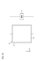
図15及び図16は、上述したX線画像検出装置3の変形例を示す。
図15及び図16に示すX線画像検出装置103において、検出部62を支持する支持体63のカバー部92には、そのほぼ全体を覆う大きさに形成された一つのバイメタル90が設けられている。コンソール4にて設定された撮影距離SIDに応じて駆動部91から電流を印加されたバイメタル90は、X線焦点16を中心とする球面に沿うように湾曲する。バイメタル90が湾曲するのに伴って、支持体63、及びこれに支持された検出部62もまた、X線焦点16を中心とする球面に沿うように湾曲する。それにより、各柱状結晶82は、X線焦点16を指向し、そこに入射するX線に対してほぼ平行とされる。それにより、X線が複数の柱状結晶82に跨ってシンチレータ60内を進行することが防止され、画像の鮮鋭度がより向上する。
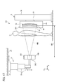
図17は、上述したX線撮影装置1の変形例を示し、図18は、図17のX線撮影装置のX線画像検出装置の構成を示す。
X線撮影装置201は、複数のX線源202を有している。コンソール4の制御装置40による制御によって、これらのX線源202からX線が順次放射され、X線焦点位置は、X線源202の切り換えに伴って順次移動する。
X線画像検出装置203において、検出部62を支持する支持体63のカバー部92は、複数の領域に区分されており、各領域にバイメタル90が設けられている。図示の例では、x方向及びy方向に、それぞれ3つの領域に区分されており、各領域にバイメタル90が設けられている。そして、駆動部91は、X線焦点位置に応じて、各バイメタル90への印加電流をバイメタル90毎に独立して制御するように構成されている。
図19は、X線画像検出装置203における検出部62の湾曲を模式的に示す。
駆動部91から各バイメタル90に独立に制御された電流が印加されることによって、検出部62の曲率半径、及び検出部62の中心と曲率中心とを結ぶ直線の方向を種々に変化させることができる。
例えば、各領域のバイメタル90への印加電流が等しい場合には、検出部62の中心部に関して略対称に検出部62が湾曲する。その際の検出部62の中心部とこの中心部における曲率中心とを結ぶ直線は、z方向に略沿っている(FIG.19A)。一方、y方向に関して中央の列領域のバイメタル90への印加電流に対して、いずれか一方の側の列領域のバイメタル90への印加電流を大きくし、他方の側の列領域のバイメタル90への印加電流を小さくした場合には、検出部62の中心に関して非対称に検出部62が湾曲する。その際の検出部62の中心と曲率中心とを結ぶ直線は、z方向に対して傾斜する(FIG.19B,C)。
このように、X線焦点位置に応じて各バイメタル90への印加電流を独立して制御することにより、X線源202の切り換えに伴って順次移動するX線焦点位置に検出部62の曲率中心を一致させることができる。それにより、異なるX線焦点位置から放射線に対して、シンチレータ60の各柱状結晶82を、そこに入射するX線に対してほぼ平行とすることができる。
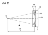
図20は、上述したX線画像検出装置3の他の変形例を示す。
上述したX線画像検出装置3及びその変形例においては、検出部62を湾曲させるための被駆動部材として、外部刺激としての熱により湾曲するバイメタル等を用いた例を説明したが、外部刺激により伸縮する被駆動部材を用いることができ、そのような被駆動部材としては、例えば高分子ゲルの体積相転移を利用した人工筋肉やピエゾ素子が例示でき、これらは、外部刺激としての印加電圧によって伸縮する。
図18に示すX線画像検出装置303において、検出部62を支持する支持体63の外周部は、筐体64の内壁に固定されている。そして、支持体63のカバー部92の中央部に人工筋肉390が設けられている。
人工筋肉390は、その伸縮方向の一端を支持体63に接続され、他端を支持体63に対向する筐体64の内壁に固定されている。駆動部(図示せず)は、撮影距離SIDに応じて、人工筋肉390への印加電圧を制御するように構成されている。撮影距離SIDに応じて駆動部91から電圧を印加された人工筋肉390が収縮することによって、支持体63は、X線焦点16を中心とする球面に沿うように湾曲し、これに支持された検出部62もまた、X線焦点16を中心とする球面に沿うように湾曲する。それにより、各柱状結晶82は、X線焦点16を指向し、そこに入射するX線に対してほぼ平行とされる。
なお、支持体63のカバー部92の中心部を筐体64に固定し、支持体63の外周部を複数の人工筋肉390によって支持するように構成し、各人工筋肉390への印加電圧を人工筋肉390毎に独立して制御するように構成することもできる。それによれば、上述したX線撮影装置201におけるX線画像検出装置203と同様に、X線焦点位置に応じて各人工筋肉390への印加電圧を独立して制御することによって、X線源202の切り換えに伴って順次移動するX線焦点位置に検出部62の曲率中心を一致させることができる。
上述の各放射線画像検出装置は、放射線画像を高感度、高精細に検出しうるため、低放射線照射量で鮮鋭な画像を検出することを要求される、マンモグラフィなどの医療診断用のX線撮影装置をはじめ、様々な装置に組み込んで使用することができる。例えば、工業用のX線撮影装置として非破壊検査に用いたり、或いは、電磁波以外の粒子線(α線、β線、γ線)の検出装置として用いたりすることができ、その応用範囲は広い。
以下、センサパネル61を構成する各要素に用いることのできる材料について説明する。
[光電変換素子]
上述した光電変換素子70の光導電層73(図3参照)としては、例えばアモルファスシリコン等の無機半導体材料が用いられることが多いが、例えば特開2009-32854号公報に記載された有機光電変換(OPC;Organic photoelectric conversion)材料も用いることができる。このOPC材料により形成された膜(以下、OPC膜という)を光導電層73として使用できる。OPC膜は、有機光電変換材料を含み、蛍光体層から発せられた光を吸収し、吸収した光に応じた電荷を発生する。このように有機光電変換材料を含むOPC膜であれば、可視域にシャープな吸収スペクトルを持ち、蛍光体層による発光以外の電磁波がOPC膜に吸収されることがほとんどなく、X線等の放射線がOPC膜で吸収されることによって発生するノイズを効果的に抑制することができる。
上述した光電変換素子70の光導電層73(図3参照)としては、例えばアモルファスシリコン等の無機半導体材料が用いられることが多いが、例えば特開2009-32854号公報に記載された有機光電変換(OPC;Organic photoelectric conversion)材料も用いることができる。このOPC材料により形成された膜(以下、OPC膜という)を光導電層73として使用できる。OPC膜は、有機光電変換材料を含み、蛍光体層から発せられた光を吸収し、吸収した光に応じた電荷を発生する。このように有機光電変換材料を含むOPC膜であれば、可視域にシャープな吸収スペクトルを持ち、蛍光体層による発光以外の電磁波がOPC膜に吸収されることがほとんどなく、X線等の放射線がOPC膜で吸収されることによって発生するノイズを効果的に抑制することができる。
OPC膜を構成する有機光電変換材料は、蛍光体層で発光した光を最も効率良く吸収するために、その吸収ピーク波長が、蛍光体層の発光ピーク波長と近いほど好ましい。有機光電変換材料の吸収ピーク波長と蛍光体層の発光ピーク波長とが一致することが理想的であるが、双方の差が小さければ蛍光体層から発された光を十分に吸収することが可能である。具体的には、有機光電変換材料の吸収ピーク波長と、蛍光体層の放射線に対する発光ピーク波長との差が、10nm以内であることが好ましく、5nm以内であることがより好ましい。
このような条件を満たすことが可能な有機光電変換材料としては、例えば、アリーリデン系有機化合物、キナクリドン系有機化合物、及びフタロシアニン系有機化合物が挙げられる。例えばキナクリドンの可視域における吸収ピーク波長は560nmであるため、有機光電変換材料としてキナクリドンを用い、蛍光体層の材料としてCsI(Tl)を用いれば、上記ピーク波長の差を5nm以内にすることが可能となり、OPC膜で発生する電荷量をほぼ最大にすることができる。
バイアス電極74a及び電荷収集電極74bの間に設けられる有機層の少なくとも一部をOPC膜によって構成することができる。この有機層は、より具体的には、電磁波を吸収する部位、光電変換部位、電子輸送部位、正孔輸送部位、電子ブロッキング部位、正孔ブロッキング部位、結晶化防止部位、電極、及び層間接触改良部位等の積み重ね若しくは混合により形成することができる。
上記有機層は、有機p型化合物又は有機n型化合物を含有することが好ましい。有機p型半導体(化合物)は、主に正孔輸送性有機化合物に代表されるドナー性有機半導体(化合物)であり、電子を供与しやすい性質がある有機化合物をいう。更に詳しくは2つの有機材料を接触させて用いたときにイオン化ポテンシャルの小さい方の有機化合物をいう。したがって、ドナー性有機化合物としては、電子供与性のある有機化合物であればいずれの有機化合物も使用可能である。例えば、トリアリールアミン化合物、ベンジジン化合物、ピラゾリン化合物、スチリルアミン化合物、ヒドラゾン化合物、トリフェニルメタン化合物、カルバゾール化合物、ポリシラン化合物、チオフェン化合物、フタロシアニン化合物、シアニン化合物、メロシアニン化合物、オキソノール化合物、ポリアミン化合物、インドール化合物、ピロール化合物、ピラゾール化合物、ポリアリーレン化合物、縮合芳香族炭素環化合物(ナフタレン誘導体、アントラセン誘導体、フェナントレン誘導体、テトラセン誘導体、ピレン誘導体、ペリレン誘導体、フルオランテン誘導体)、含窒素ヘテロ環化合物を配位子として有する金属錯体等を用いることができる。なお、これらに限らず、n型(アクセプター性)化合物として用いた有機化合物よりもイオン化ポテンシャルの小さい有機化合物であればドナー性有機半導体として用いることができる。
有機n型半導体(化合物)は、主に電子輸送性有機化合物に代表されるアクセプター性有機半導体(化合物)であり、電子を受容しやすい性質がある有機化合物をいう。更に詳しくは2つの有機化合物を接触させて用いたときに電子親和力の大きい方の有機化合物をいう。したがって、アクセプター性有機化合物は、電子受容性のある有機化合物であればいずれの有機化合物も使用可能である。例えば、縮合芳香族炭素環化合物(ナフタレン誘導体、アントラセン誘導体、フェナントレン誘導体、テトラセン誘導体、ピレン誘導体、ペリレン誘導体、フルオランテン誘導体)、窒素原子、酸素原子、硫黄原子を含有する5ないし7員のヘテロ環化合物(例えばピリジン、ピラジン、ピリミジン、ピリダジン、トリアジン、キノリン、キノキサリン、キナゾリン、フタラジン、シンノリン、イソキノリン、プテリジン、アクリジン、フェナジン、フェナントロリン、テトラゾール、ピラゾール、イミダゾール、チアゾール、オキサゾール、インダゾール、ベンズイミダゾール、ベンゾトリアゾール、ベンゾオキサゾール、ベンゾチアゾール、カルバゾール、プリン、トリアゾロピリダジン、トリアゾロピリミジン、テトラザインデン、オキサジアゾール、イミダゾピリジン、ピラリジン、ピロロピリジン、チアジアゾロピリジン、ジベンズアゼピン、トリベンズアゼピン等)、ポリアリーレン化合物、フルオレン化合物、シクロペンタジエン化合物、シリル化合物、含窒素ヘテロ環化合物を配位子として有する金属錯体などが挙げられる。なお、これらに限らず、ドナー性有機化合物として用いた有機化合物よりも電子親和力の大きな有機化合物であればアクセプター性有機半導体として用いることができる。
p型有機色素又はn型有機色素としては、公知のものを用いることができるが、好ましくは、シアニン色素、スチリル色素、ヘミシアニン色素、メロシアニン色素(ゼロメチンメロシアニン(シンプルメロシアニン)を含む)、3核メロシアニン色素、4核メロシアニン色素、ロダシアニン色素、コンプレックスシアニン色素、コンプレックスメロシアニン色素、アロポーラー色素、オキソノール色素、ヘミオキソノール色素、スクアリウム色素、クロコニウム色素、アザメチン色素、クマリン色素、アリーリデン色素、アントラキノン色素、トリフェニルメタン色素、アゾ色素、アゾメチン色素、スピロ化合物、メタロセン色素、フルオレノン色素、フルギド色素、ペリレン色素、フェナジン色素、フェノチアジン色素、キノン色素、インジゴ色素、ジフェニルメタン色素、ポリエン色素、アクリジン色素、アクリジノン色素、ジフェニルアミン色素、キナクリドン色素、キノフタロン色素、フェノキサジン色素、フタロペリレン色素、ポルフィリン色素、クロロフィル色素、フタロシアニン色素、金属錯体色素、縮合芳香族炭素環系色素(ナフタレン誘導体、アントラセン誘導体、フェナントレン誘導体、テトラセン誘導体、ピレン誘導体、ペリレン誘導体、フルオランテン誘導体)等が挙げられる。
1対の電極間に、p型半導体層とn型半導体層とを有し、該p型半導体とn型半導体の少なくともいずれかが有機半導体であり、かつ、それらの半導体層の間に、該p型半導体及びn型半導体を含むバルクヘテロ接合構造層を中間層として有する光電変換膜(感光層)を好適に用いることができる。このように、光電変換膜において、バルクへテロ接合構造層を含ませることにより有機層のキャリア拡散長が短いという欠点を補い、光電変換効率を向上させることができる。なお、上記バルクへテロ接合構造については、特開2005-303266号公報において詳細に説明されている。
光電変換膜の厚みは、蛍光体層からの光を吸収する点では膜厚は大きいほど好ましいが、電荷分離に寄与しない割合を考慮すると、30nm以上300nm以下が好ましく、より好ましくは、50nm以上250nm以下、特に好ましくは80nm以上200nm以下である。
上述したOPC膜に関するその他の構成は、例えば、特開2009-32854号公報の記載が参考となる。
上述したOPC膜に関するその他の構成は、例えば、特開2009-32854号公報の記載が参考となる。
[スイッチ素子]
スイッチ素子71の活性層としては、例えばアモルファスシリコン等の無機半導体材料が使われることが多いが、例えば特開2009-212389号公報に記載されたように、有機材料を使用することができる。有機TFTはいかなるタイプの構造でもよいが、最も好ましいのは電界効果型トランジスタ(FET)構造である。このFET構造は、絶縁性基板上面の一部にゲート電極を設け、更に該電極を覆い、かつ電極以外の部分で基板と接するように絶縁体層を設けている。更に絶縁体層の上面に半導体活性層を設け、その上面の一部に透明ソース電極と透明ドレイン電極とを隔離して配置している。なお、この構成はトップコンタクト型素子と呼ばれるが、ソース電極とドレイン電極とが半導体活性層の下部にあるボトムコンタクト型素子も好ましく用いることができる。また、キャリアが有機半導体膜の膜厚方向に流れる縦型トランジスタ構造であってもよい。
スイッチ素子71の活性層としては、例えばアモルファスシリコン等の無機半導体材料が使われることが多いが、例えば特開2009-212389号公報に記載されたように、有機材料を使用することができる。有機TFTはいかなるタイプの構造でもよいが、最も好ましいのは電界効果型トランジスタ(FET)構造である。このFET構造は、絶縁性基板上面の一部にゲート電極を設け、更に該電極を覆い、かつ電極以外の部分で基板と接するように絶縁体層を設けている。更に絶縁体層の上面に半導体活性層を設け、その上面の一部に透明ソース電極と透明ドレイン電極とを隔離して配置している。なお、この構成はトップコンタクト型素子と呼ばれるが、ソース電極とドレイン電極とが半導体活性層の下部にあるボトムコンタクト型素子も好ましく用いることができる。また、キャリアが有機半導体膜の膜厚方向に流れる縦型トランジスタ構造であってもよい。
(活性層)
ここでいう有機半導体材料とは、半導体の特性を示す有機材料のことであり、無機材料からなる半導体と同様に、正孔(ホール)をキャリアとして伝導するp型有機半導体材料(あるいは単にp型材料、正孔輸送材料とも言う。)と、電子をキャリアとして伝導するn型有機半導体材料(あるいは単にn型材料、電子輸送材料とも言う。)がある。有機半導体材料は一般にp型材料の方が良好な特性を示すものが多く、また、一般に大気下でのトランジスタ動作安定性もp型トランジスタの方が優れているため、ここでは、p型有機半導体材料について説明する。
ここでいう有機半導体材料とは、半導体の特性を示す有機材料のことであり、無機材料からなる半導体と同様に、正孔(ホール)をキャリアとして伝導するp型有機半導体材料(あるいは単にp型材料、正孔輸送材料とも言う。)と、電子をキャリアとして伝導するn型有機半導体材料(あるいは単にn型材料、電子輸送材料とも言う。)がある。有機半導体材料は一般にp型材料の方が良好な特性を示すものが多く、また、一般に大気下でのトランジスタ動作安定性もp型トランジスタの方が優れているため、ここでは、p型有機半導体材料について説明する。
有機薄膜トランジスタの特性の一つに、有機半導体層中のキャリアの動きやすさを示すキャリア移動度(単に移動度とも言う)μがある。用途によっても異なるが、一般に移動度は高い方がよく、1.0×10⁻⁷cm2/Vs以上であることが好ましく、1.0×10-6cm2/Vs以上であることがより好ましく、1.0×10-5cm2/Vs以上であることが更に好ましい。移動度は電界効果トランジスタ(FET)素子を作製したときの特性や飛行時間計測(TOF)法により求めることができる。
前記p型有機半導体材料は、低分子材料でも高分子材料でも良いが、好ましくは低分子材料である。低分子材料は、昇華精製や再結晶、カラムクロマトグラフィーなどの様々な精製法が適用できるため高純度化が容易であること、分子構造が定まっているため秩序の高い結晶構造を取りやすいこと、などの理由から高い特性を示すものが多い。低分子材料の分子量は、好ましくは100以上5000以下、より好ましくは150以上3000以下、更に好ましくは200以上2000以下である。
このようなp型有機半導体材料としては、フタロシアニン化合物又はナフタロシアニン化合物を例示することができ、具体例を以下に示す。なお、Mは金属原子、Buはブチル基、Prはプロピル基、Etはエチル基、Phはフェニル基をそれぞれ表す。

(活性層以外のスイッチ素子の構成要素)
ゲート電極、ソース電極、又はドレイン電極を構成する材料としては、必要な導電性を有するものであれば特に制限はないが、例えば、ITO(インジウムドープ酸化スズ)、IZO(インジウムドープ酸化亜鉛)、SnO2、ATO(アンチモンドープ酸化スズ)、ZnO、AZO(アルミニウムドープ酸化亜鉛)、GZO(ガリウムドープ酸化亜鉛)、TiO2、FTO(フッ素ドープ酸化スズ)などの透明導電性酸化物、PEDOT/PSS(ポリ(3,4-エチレンジオキシチオフェン)/ポリスチレンスルホン酸)などの透明導電性ポリマー、カーボンナノチューブなどの炭素材料が挙げられる。これらの電極材料は、例えば真空蒸着法、スパッタリング、溶液塗布法等の方法で成膜することができる。
ゲート電極、ソース電極、又はドレイン電極を構成する材料としては、必要な導電性を有するものであれば特に制限はないが、例えば、ITO(インジウムドープ酸化スズ)、IZO(インジウムドープ酸化亜鉛)、SnO2、ATO(アンチモンドープ酸化スズ)、ZnO、AZO(アルミニウムドープ酸化亜鉛)、GZO(ガリウムドープ酸化亜鉛)、TiO2、FTO(フッ素ドープ酸化スズ)などの透明導電性酸化物、PEDOT/PSS(ポリ(3,4-エチレンジオキシチオフェン)/ポリスチレンスルホン酸)などの透明導電性ポリマー、カーボンナノチューブなどの炭素材料が挙げられる。これらの電極材料は、例えば真空蒸着法、スパッタリング、溶液塗布法等の方法で成膜することができる。
絶縁層に用いられる材料としては、必要な絶縁効果を有するものであれば特に制限はないが、例えば、二酸化ケイ素、窒化ケイ素、アルミナなどの無機材料、ポリエステル(PEN(ポリエチレンナフタレート)、PET(ポリエチレンテレフタレート)など)、ポリカーボネート、ポリイミド、ポリアミド、ポリアクリレート、エポキシ樹脂、ポリパラキシリレン樹脂、ノボラック樹脂、PVA(ポリビニルアルコール)、PS(ポリスチレン)、などの有機材料が挙げられる。これらの絶縁膜材料は、例えば真空蒸着法、スパッタリング、溶液塗布法等の方法で成膜することができる。
上述した有機TFTに関するその他の構成は、例えば、特開2009-212389号公報の記載が参考となる。
上述した有機TFTに関するその他の構成は、例えば、特開2009-212389号公報の記載が参考となる。
また、スイッチ素子71の活性層には、例えば特開2010-186860号公報に記載された非晶質酸化物も使用することができる。ここで、特開2010-186860号に記載された電界効果型トランジスタが有する非晶質酸化物含有の活性層について示す。この活性層は、電子又はホールの移動する電界効果型トランジスタのチャネル層として機能する。
活性層は、非晶質酸化物半導体を含んだ構成とされている。この非晶質酸化物半導体は、低温で成膜可能であるために、可撓性のある基板上に好適に形成される。活性層に用いられる非晶質酸化物半導体としては、好ましくはIn、Sn、Zn、又はCdよりなる群より選ばれる少なくとも1種の元素を含む非晶質酸化物であり、より好ましくは、In、Sn、Znよりなる群より選ばれる少なくとも1種を含む非晶質酸化物、更に好ましくは、In、Znよりなる群より選ばれる少なくとも1種を含む非晶質酸化物である。
活性層に用いられる非晶質酸化物としては、具体的には、In2O3、ZnO,SnO2、CdO,Indium-Zinc-Oxide(IZO)、Indium-Tin-Oxide(ITO)、Gallium-Zinc-Oxide(GZO)、Indium-Gallium-Oxide(IGO)、Indium-Gallium-Zinc-Oxide(IGZO)が挙げられる。
活性層の成膜方法としては、酸化物半導体の多結晶焼結体をターゲットとして、気相成膜法を用いるのが好ましい。気相成膜法の中でも、スパッタリング法、パルスレーザー蒸着法(PLD法)が適している。更に、量産性の観点から、スパッタリング法が好ましい。例えば、RFマグネトロンスパッタリング蒸着法により、真空度及び酸素流量を制御して成膜される。
成膜された活性層は、周知のX線回折法によりアモルファス膜であることが確認される。活性層の組成比は、RBS(ラザフォード後方散乱)分析法により求められる。
また、この活性層の電気伝導度は、好ましくは10-4Scm-1以上102Scm-1未満であり、より好ましくは10-1Scm-1以上102Scm-1未満である。この活性層の電気伝導度の調整方法としては、公知の酸素欠陥による調整方法や、組成比による調整方法、不純物による調整方法、酸化物半導体材料による調整方法が挙げられる。
上述した非晶質酸化物に関するその他の構成は、例えば、特開2010-186860号公報の記載が参考となる。
上述した非晶質酸化物に関するその他の構成は、例えば、特開2010-186860号公報の記載が参考となる。
[絶縁性フレキシブル基板]
絶縁性フレキシブル基板としては、プラスチックフィルムなどが挙げられる。プラスチックフィルムとしては、例えばポリエチレンテレフタレート(PET)、ポリエチレンナフタレート(PEN)、ポリエーテルスルホン(PES)、ポリエーテルイミド、ポリエーテルエーテルケトン、ポリフェニレンスルフィド、ポリアリレート、ポリイミド、ポリカーボネート(PC)、セルローストリアセテート(TAC)、セルロースアセテートプロピオネート(CAP)等からなるフィルム等が挙げられる。また、これらのプラスチックフィルムに、有機あるいは無機のフィラーを含有させてもよい。また、フレキシブルでかつ低熱膨張、高強度といった、既存のガラスやプラスチックでは得られない特性を有するアラミド、バイオナノファイバーなどを用いて形成されたフレキシブル基板も好適に使用しうる。
絶縁性フレキシブル基板としては、プラスチックフィルムなどが挙げられる。プラスチックフィルムとしては、例えばポリエチレンテレフタレート(PET)、ポリエチレンナフタレート(PEN)、ポリエーテルスルホン(PES)、ポリエーテルイミド、ポリエーテルエーテルケトン、ポリフェニレンスルフィド、ポリアリレート、ポリイミド、ポリカーボネート(PC)、セルローストリアセテート(TAC)、セルロースアセテートプロピオネート(CAP)等からなるフィルム等が挙げられる。また、これらのプラスチックフィルムに、有機あるいは無機のフィラーを含有させてもよい。また、フレキシブルでかつ低熱膨張、高強度といった、既存のガラスやプラスチックでは得られない特性を有するアラミド、バイオナノファイバーなどを用いて形成されたフレキシブル基板も好適に使用しうる。
(アラミド)
アラミド材料は、ガラス転移温度315℃という高い耐熱性、ヤング率が10GPaという高い剛性、熱膨張率が-3~5ppm/℃という高い寸法安定性を有する。このため、アラミド製のフィルムを用いると、一般的な樹脂フィルムを用いる場合と比べて、半導体層の高品質の成膜が容易に行える。また、アラミド材料の高耐熱性により、電極材料を高温硬化させて低抵抗化できる。更に、ハンダのリフロー工程を含むICの自動実装にも対応できる。また更に、ITO(indium tin oxide)やガス・バリア膜、ガラス基板と熱膨張係数が近いために、製造後の反りが少ない。そして、割れにくい。ここで、ハロゲンを含まないハロゲンフリー(JPCA-ES01-2003の規定に適合)なアラミド材料を用いることが環境負荷低減の点で好ましい。アラミドフィルムは、ガラス基板やPET基板と積層されてもよいし、デバイスの筐体に貼り付けられてもよい。
アラミド材料は、ガラス転移温度315℃という高い耐熱性、ヤング率が10GPaという高い剛性、熱膨張率が-3~5ppm/℃という高い寸法安定性を有する。このため、アラミド製のフィルムを用いると、一般的な樹脂フィルムを用いる場合と比べて、半導体層の高品質の成膜が容易に行える。また、アラミド材料の高耐熱性により、電極材料を高温硬化させて低抵抗化できる。更に、ハンダのリフロー工程を含むICの自動実装にも対応できる。また更に、ITO(indium tin oxide)やガス・バリア膜、ガラス基板と熱膨張係数が近いために、製造後の反りが少ない。そして、割れにくい。ここで、ハロゲンを含まないハロゲンフリー(JPCA-ES01-2003の規定に適合)なアラミド材料を用いることが環境負荷低減の点で好ましい。アラミドフィルムは、ガラス基板やPET基板と積層されてもよいし、デバイスの筐体に貼り付けられてもよい。
アラミドの分子間の凝集力(水素結合力)の高さによる溶媒への低溶解性を分子設計によって解決することにより、無色透明で薄いフィルムへの成形が容易とされたアラミド材料についても、好適に用いることができる。モノマーユニットの秩序性、及び芳香環上の置換基種・位置を制御する分子設計により、アラミド材料の高剛性や寸法安定性に繋がる直線性の高い棒状の分子構造を維持しつつ、溶解性が良い成形の容易さが得られる。この分子設計により、ハロゲンフリーをも実現できる。
また、フィルムの面内方向の特性が最適化されたアラミド材料についても、好適に用いることができる。成型中に逐次変化するアラミドフィルムの強度に応じて、溶液キャスト、縦延伸、横延伸の工程ごとに張力条件を制御することにより、直線性の高い棒状分子構造であって物性に異方性が生じやすいアラミドフィルムの面内方向の特性をバランスできる。
具体的に、溶液キャスト工程では、溶媒の乾燥速度の制御による面内厚み方向の物性の等方化、溶媒を含んだ状態のフィルムの強度とキャスト・ドラムからの剥離強度の最適化、を図る。縦延伸工程では、延伸中に逐次変化するフィルムの強度、溶媒の残留量に応じた延伸条件を精密に制御する。横延伸工程では、加熱によって変化するフィルム強度の変化に応じた横延伸の条件の制御、フィルムの残留応力を緩和するための横延伸の条件の制御を図る。このようなアラミド材料の使用により、成型後のアラミドフィルムがカールしてしまう問題を解決できる。
上記の成形容易さに対する工夫、及びフィルム面内方向の特性のバランスに対する工夫のいずれにおいても、アラミドならではの直線性の高い棒状の分子構造が維持されているので、熱膨張係数を低く維持できる。製膜時の延伸条件の変更などにより、熱膨張係数を更に低減することも可能である。
(バイオナノファイバー)
ナノファイバーは、光の波長に対して十分に小さなコンポーネントは光散乱を生じないことから、透明でフレキシブルな樹脂材料の補強として用いることができる。そして、ナノファイバーの中でも、バクテリア(酢酸菌、Acetobacter Xylinum)が産出するセルロースミクロフィブリル束は、幅50nmと、可視光波長に対して約1/10のサイズでかつ、高強度、高弾性、低熱膨である特徴を有しており、このバクテリアセルロースと透明樹脂との複合材料(バイオナノファイバーということがある)を好適に用いることができる。
ナノファイバーは、光の波長に対して十分に小さなコンポーネントは光散乱を生じないことから、透明でフレキシブルな樹脂材料の補強として用いることができる。そして、ナノファイバーの中でも、バクテリア(酢酸菌、Acetobacter Xylinum)が産出するセルロースミクロフィブリル束は、幅50nmと、可視光波長に対して約1/10のサイズでかつ、高強度、高弾性、低熱膨である特徴を有しており、このバクテリアセルロースと透明樹脂との複合材料(バイオナノファイバーということがある)を好適に用いることができる。
バクテリアセルロースシートにアクリル樹脂、エポキシ樹脂等の透明樹脂を含浸・硬化させることで、繊維を約60~70%と高い比率で含有しながら、波長500nmで約90%の光透過率を示す透明バイオナノファイバーが得られる。このバイオナノファイバーにより、シリコン結晶に匹敵する低い熱膨張係数(約3~7ppm)、鋼鉄並の強度(約460MPa)、及び高弾性(約30GPa)が得られる。
上述したバイオナノファイバーに関する構成は、例えば、特開2008-34556号公報の記載が参考となる。
上述したバイオナノファイバーに関する構成は、例えば、特開2008-34556号公報の記載が参考となる。
以上、説明したように、本明細書には、下記(1)から(13)の放射線画像検出装置が開示されている。
(1) 放射線露光によって蛍光を発する蛍光物質を含有した蛍光体と、前記蛍光体が密接して設けられ、前記蛍光体が発する蛍光を検出するセンサパネルと、を備える放射線画像検出器であって、前記蛍光体は、前記蛍光物質の結晶が柱状に成長してなる柱状結晶の集合体からなる柱状部を含み、前記センサパネルの前記蛍光体とは反対側に放射線入射面が設けられ、前記センサパネルは、可撓性を有し、前記放射入射面側に曲率中心が位置するように湾曲された放射線画像検出装置。
(2) 上記(1)の放射線画像検出装置であって、前記センサパネルを支持し、曲率中心の位置を可変に前記センサパネルを湾曲させる湾曲部を更に備える放射線画像検出装置。
(3) 上記(2)の放射線画像検出装置であって、前記湾曲部は、前記センサパネルの曲率半径を可変に前記センサパネルを湾曲させる放射線画像検出装置。
(4) 上記(2)又は(3)の放射線画像検出装置であって、前記湾曲部は、前記センサパネルの中心と曲率中心とを結ぶ直線の方向を可変に前記センサパネルを湾曲させる放射線画像検出装置。
(5) 上記(2)から(4)のいずれか一つの放射線画像検出装置であって、前記湾曲部は、物理的刺激に応じて湾曲し、前記センサパネルに添着される少なくとも一つの被駆動体を含む放射線画像検出装置。
(6) 上記(5)の放射線画像検出装置であって、前記被駆動体は、バイメタルである放射線画像検出装置。
(7) 上記(6)の放射線画像検出装置であって、前記湾曲部は、前記バイメタルに電流を印加する駆動部を有する放射線画像検出装置。
(8) 上記(2)から(4)のいずれか一つの放射線画像検出装置であって、前記湾曲部は、物理的刺激に応じて伸縮し、一端を前記センサパネルに接続され、他端を固定された少なくとも一つの被駆動体を含む放射線画像検出装置。
(9) 上記(5)から(8)のいずれか一つの放射線画像検出装置であって、前記湾曲部は、複数の前記被駆動体を有し、各被駆動体に対して独立に前記物理的刺激を与える放射線画像検出装置。
(10) 上記(5)から(9)のいずれか一つの放射線画像検出装置であって、前記湾曲部は、前記センサパネルにおいて前記蛍光体に密接する面とは反対側の面を覆うカバー部、及び前記センサパネルの縁部を係止する係止部を含んで構成され、前記センサパネルを支持する支持体を有しており、前記被駆動体は、前記カバー部に設けられている放射線画像検出装置。
(11) 上記(10)の放射線画像検出装置であって、前記支持体は、可撓性を有する放射線画像検出装置。
(12) 上記(1)から(11)のいずれか一つの放射線画像検出装置であって、前記蛍光体は、前記柱状部に比べて空隙率が小さい非柱状部を更に含み、前記非柱状部において前記センサパネルに密接している放射線画像検出装置。
(13) 上記(12)の放射線画像検出装置であって、前記非柱状部の厚みは、5μm~50μmである放射線画像検出装置。
(2) 上記(1)の放射線画像検出装置であって、前記センサパネルを支持し、曲率中心の位置を可変に前記センサパネルを湾曲させる湾曲部を更に備える放射線画像検出装置。
(3) 上記(2)の放射線画像検出装置であって、前記湾曲部は、前記センサパネルの曲率半径を可変に前記センサパネルを湾曲させる放射線画像検出装置。
(4) 上記(2)又は(3)の放射線画像検出装置であって、前記湾曲部は、前記センサパネルの中心と曲率中心とを結ぶ直線の方向を可変に前記センサパネルを湾曲させる放射線画像検出装置。
(5) 上記(2)から(4)のいずれか一つの放射線画像検出装置であって、前記湾曲部は、物理的刺激に応じて湾曲し、前記センサパネルに添着される少なくとも一つの被駆動体を含む放射線画像検出装置。
(6) 上記(5)の放射線画像検出装置であって、前記被駆動体は、バイメタルである放射線画像検出装置。
(7) 上記(6)の放射線画像検出装置であって、前記湾曲部は、前記バイメタルに電流を印加する駆動部を有する放射線画像検出装置。
(8) 上記(2)から(4)のいずれか一つの放射線画像検出装置であって、前記湾曲部は、物理的刺激に応じて伸縮し、一端を前記センサパネルに接続され、他端を固定された少なくとも一つの被駆動体を含む放射線画像検出装置。
(9) 上記(5)から(8)のいずれか一つの放射線画像検出装置であって、前記湾曲部は、複数の前記被駆動体を有し、各被駆動体に対して独立に前記物理的刺激を与える放射線画像検出装置。
(10) 上記(5)から(9)のいずれか一つの放射線画像検出装置であって、前記湾曲部は、前記センサパネルにおいて前記蛍光体に密接する面とは反対側の面を覆うカバー部、及び前記センサパネルの縁部を係止する係止部を含んで構成され、前記センサパネルを支持する支持体を有しており、前記被駆動体は、前記カバー部に設けられている放射線画像検出装置。
(11) 上記(10)の放射線画像検出装置であって、前記支持体は、可撓性を有する放射線画像検出装置。
(12) 上記(1)から(11)のいずれか一つの放射線画像検出装置であって、前記蛍光体は、前記柱状部に比べて空隙率が小さい非柱状部を更に含み、前記非柱状部において前記センサパネルに密接している放射線画像検出装置。
(13) 上記(12)の放射線画像検出装置であって、前記非柱状部の厚みは、5μm~50μmである放射線画像検出装置。
また、本明細書には、下記(14)及び(15)の放射線撮影装置が開示されている。
(14) 上記(1)から(13)のいずれか一つの放射線画像検出装置と、前記放射線画像検出装置に向けて放射線を照射する放射線源と、を備え、前記センサパネルの曲率中心が、前記放射線焦点に一致している放射線撮影装置。
(15) 上記(2)から(9)のいずれか一つの放射線画像検出装置と、前記放射線画像検出装置に向けて放射線を照射する放射線源と、前記放射線画像検出装置に対する前記放射線源の相対位置を検出する検出手段と、を備え、前記湾曲部は、前記検出手段によって検出される放射線源の相対位置に応じて前記センサパネルの曲率中心の位置が変化するように、前記センサパネルを湾曲させる放射線撮影装置。
(15) 上記(2)から(9)のいずれか一つの放射線画像検出装置と、前記放射線画像検出装置に向けて放射線を照射する放射線源と、前記放射線画像検出装置に対する前記放射線源の相対位置を検出する検出手段と、を備え、前記湾曲部は、前記検出手段によって検出される放射線源の相対位置に応じて前記センサパネルの曲率中心の位置が変化するように、前記センサパネルを湾曲させる放射線撮影装置。
本発明によれば、放射入射面側に曲率中心が位置するように湾曲されたセンサパネルに対して、蛍光体はその外径側に配置され、蛍光体を形成する柱状結晶の集合体の先端部間の隙間は拡大される。よって、隣り合う柱状結晶の先端部同士の接触が回避され、柱状結晶の損傷が防止される。それにより、撮影距離が比較的短い場合にも、撮影距離に合わせて放射線に対して各柱状結晶を平行に配置することができ、画像の鮮鋭度を向上させることができる。
本発明を詳細にまた特定の実施態様を参照して説明したが、本発明の精神と範囲を逸脱することなく様々な変更や修正を加えることができることは当業者にとって明らかである。
本出願は、2011年02月21日出願の日本特許出願(特願2011-035227)に基づくものであり、その内容はここに参照として取り込まれる。
本出願は、2011年02月21日出願の日本特許出願(特願2011-035227)に基づくものであり、その内容はここに参照として取り込まれる。
1 X線撮影システム
2 X線源
3 X線画像検出装置
4 コンソール
5 X線源保持装置
6 スタンド
10 X線源制御部
11 高電圧発生器
12 X線管
13 コリメータ
14 コリメータユニット
15 回転陽極
16 X線焦点
20 天井レール
21 台車部
22 支柱部
30 本体
31 保持部
40 制御装置
41 入力装置
42 画像処理部
43 記憶部
44 モニタ
46 バス
60 シンチレータ
61 センサパネル
62 検出部
63 支持体
64 筐体
65 湾曲部
70 光電変換素子
71 スイッチ素子
72 フレキシブルTFT基板
73 光導電層
74a バイアス電極
74b 電荷収集電極
75 平坦化層
76 ゲート線
77 信号線
78 接続端子
79 接続回路
80 柱状部
81 非柱状部
82 柱状結晶
83 基板
90 バイメタル(被駆動部材)
91 駆動部
92 カバー部
93 係止部
2 X線源
3 X線画像検出装置
4 コンソール
5 X線源保持装置
6 スタンド
10 X線源制御部
11 高電圧発生器
12 X線管
13 コリメータ
14 コリメータユニット
15 回転陽極
16 X線焦点
20 天井レール
21 台車部
22 支柱部
30 本体
31 保持部
40 制御装置
41 入力装置
42 画像処理部
43 記憶部
44 モニタ
46 バス
60 シンチレータ
61 センサパネル
62 検出部
63 支持体
64 筐体
65 湾曲部
70 光電変換素子
71 スイッチ素子
72 フレキシブルTFT基板
73 光導電層
74a バイアス電極
74b 電荷収集電極
75 平坦化層
76 ゲート線
77 信号線
78 接続端子
79 接続回路
80 柱状部
81 非柱状部
82 柱状結晶
83 基板
90 バイメタル(被駆動部材)
91 駆動部
92 カバー部
93 係止部
Claims (15)
- 放射線露光によって蛍光を発する蛍光物質を含有した蛍光体と、
前記蛍光体が密接して設けられ、前記蛍光体が発する蛍光を検出するセンサパネルと、
を備える放射線画像検出器であって、
前記蛍光体は、前記蛍光物質の結晶が柱状に成長してなる柱状結晶の集合体からなる柱状部を含み、
前記センサパネルの前記蛍光体とは反対側に放射線入射面が設けられ、
前記センサパネルは、可撓性を有し、前記放射入射面側に曲率中心が位置するように湾曲された放射線画像検出装置。 - 請求項1に記載の放射線画像検出装置であって、
前記センサパネルを支持し、曲率中心の位置を可変に前記センサパネルを湾曲させる湾曲部をさらに備える放射線画像検出装置。 - 請求項2に記載の放射線画像検出装置であって、
前記湾曲部は、前記センサパネルの曲率半径を可変に前記センサパネルを湾曲させる放射線画像検出装置。 - 請求項2又は3に記載の放射線画像検出装置であって、
前記湾曲部は、前記センサパネルの中心と曲率中心とを結ぶ直線の方向を可変に前記センサパネルを湾曲させる放射線画像検出装置。 - 請求項2から4のいずれか一項に記載の放射線画像検出装置であって、
前記湾曲部は、物理的刺激に応じて湾曲し、前記センサパネルに添着される少なくとも一つの被駆動体を含む放射線画像検出装置。 - 請求項5に記載の放射線画像検出装置であって、
前記被駆動体は、バイメタルである放射線画像検出装置。 - 請求項6に記載の放射線画像検出装置であって、
前記湾曲部は、前記バイメタルに電流を印加する駆動部を有する放射線画像検出装置。 - 請求項2から4のいずれか一項に記載の放射線画像検出装置であって、
前記湾曲部は、物理的刺激に応じて伸縮し、一端を前記センサパネルに接続され、他端を固定された少なくとも一つの被駆動体を含む放射線画像検出装置。 - 請求項5から8のいずれか一項に記載の放射線画像検出装置であって、
前記湾曲部は、複数の前記被駆動体を有し、各被駆動体に対して独立に前記物理的刺激を与える放射線画像検出装置。 - 請求項5から9のいずれか一項に記載の放射線画像検出装置であって、
前記湾曲部は、前記センサパネルにおいて前記蛍光体に密接する面とは反対側の面を覆うカバー部、及び前記センサパネルの縁部を係止する係止部を含んで構成され、前記センサパネルを支持する支持体を有しており、
前記被駆動体は、前記カバー部に設けられている放射線画像検出装置。 - 請求項10に記載の放射線画像検出装置であって、
前記支持体は、可撓性を有する放射線画像検出装置。 - 請求項1から11のいずれか一項に記載の放射線画像検出装置であって、
前記蛍光体は、前記柱状部に比べて空隙率が小さい非柱状部をさらに含み、前記非柱状部において前記センサパネルに密接している放射線画像検出装置。 - 請求項12に記載の放射線画像検出装置であって、
前記非柱状部の厚みは、5μm~50μmである放射線画像検出装置。 - 請求項1から13のいずれか一項に記載の放射線画像検出装置と、
前記放射線画像検出装置に向けて放射線を照射する放射線源と、
を備え、
前記センサパネルの曲率中心が、前記放射線源の焦点に一致している放射線撮影装置。 - 請求項2から9のいずれか一項に記載の放射線画像検出装置と、
前記放射線画像検出装置に向けて放射線を照射する放射線源と、
前記放射線画像検出装置に対する前記放射線源の相対位置を検出する検出手段と、
を備え、
前記湾曲部は、前記検出手段によって検出される放射線源の相対位置に応じて前記センサパネルの曲率中心の位置が変化するように、前記センサパネルを湾曲させる放射線撮影装置。
Priority Applications (2)
| Application Number | Priority Date | Filing Date | Title |
|---|---|---|---|
| CN2012800097970A CN103384838A (zh) | 2011-02-21 | 2012-02-20 | 放射线图像检测装置和放射线摄影装置 |
| US13/972,009 US8803101B2 (en) | 2011-02-21 | 2013-08-21 | Radiological image detection apparatus and radiation imaging apparatus |
Applications Claiming Priority (2)
| Application Number | Priority Date | Filing Date | Title |
|---|---|---|---|
| JP2011-035227 | 2011-02-21 | ||
| JP2011035227A JP2012173128A (ja) | 2011-02-21 | 2011-02-21 | 放射線画像検出装置及び放射線撮影装置 |
Related Child Applications (1)
| Application Number | Title | Priority Date | Filing Date |
|---|---|---|---|
| US13/972,009 Continuation US8803101B2 (en) | 2011-02-21 | 2013-08-21 | Radiological image detection apparatus and radiation imaging apparatus |
Publications (1)
| Publication Number | Publication Date |
|---|---|
| WO2012115039A1 true WO2012115039A1 (ja) | 2012-08-30 |
Family
ID=46720816
Family Applications (1)
| Application Number | Title | Priority Date | Filing Date |
|---|---|---|---|
| PCT/JP2012/053970 Ceased WO2012115039A1 (ja) | 2011-02-21 | 2012-02-20 | 放射線画像検出装置及び放射線撮影装置 |
Country Status (4)
| Country | Link |
|---|---|
| US (1) | US8803101B2 (ja) |
| JP (1) | JP2012173128A (ja) |
| CN (1) | CN103384838A (ja) |
| WO (1) | WO2012115039A1 (ja) |
Cited By (1)
| Publication number | Priority date | Publication date | Assignee | Title |
|---|---|---|---|---|
| JP2022062127A (ja) * | 2013-07-26 | 2022-04-19 | 株式会社半導体エネルギー研究所 | 発光装置 |
Families Citing this family (22)
| Publication number | Priority date | Publication date | Assignee | Title |
|---|---|---|---|---|
| JP2013050364A (ja) * | 2011-08-30 | 2013-03-14 | Fujifilm Corp | 放射線画像検出装置 |
| KR102279966B1 (ko) * | 2013-12-23 | 2021-07-21 | 주식회사 바텍 | 치과용 엑스선 촬영장치 |
| JP2015230175A (ja) * | 2014-06-03 | 2015-12-21 | コニカミノルタ株式会社 | 放射線画像検出装置及びその製造方法 |
| US10712454B2 (en) * | 2014-07-25 | 2020-07-14 | General Electric Company | X-ray detectors supported on a substrate having a metal barrier |
| KR102301941B1 (ko) * | 2014-08-08 | 2021-09-16 | 주식회사 레이언스 | 이미지센서 및 이를 이용한 구강센서장치 |
| KR101963121B1 (ko) | 2014-12-02 | 2019-03-28 | 주식회사 레이언스 | 구강내 센서 |
| EP3133422B1 (en) * | 2015-08-17 | 2021-05-05 | Nokia Technologies Oy | Flexible pixel array controlled by conductive shape memory material |
| BR112018014159A2 (pt) * | 2016-05-16 | 2018-12-11 | Sintokogio Ltd | método de processamento de tratamento de superfície e dispositivo de processamento de tratamento de superfície |
| EP3507621B1 (en) * | 2016-08-31 | 2024-03-06 | BOE Technology Group Co., Ltd. | Radiation detector and fabricating method thereof |
| CN106443751B (zh) * | 2016-09-29 | 2018-12-18 | 中国核动力研究设计院 | 固化桶表面剂量率检测装置及其检测方法 |
| GB201621750D0 (en) | 2016-12-20 | 2017-02-01 | Univ York | Charged Particle Detector |
| JP2017122733A (ja) * | 2017-03-02 | 2017-07-13 | コニカミノルタ株式会社 | X線検出器 |
| CN108010928A (zh) * | 2017-11-02 | 2018-05-08 | 上海奕瑞光电子科技股份有限公司 | 一种柔性x射线传感器闪烁体层的直接生长方法 |
| KR102051957B1 (ko) * | 2017-11-13 | 2019-12-04 | 주식회사 토비스 | 곡면 디텍터의 제조방법 |
| DE102018200845B4 (de) * | 2018-01-19 | 2021-05-06 | Siemens Healthcare Gmbh | Montageverfahren für die Herstellung eines Röntgendetektors, Röntgendetektor und Röntgengerät |
| JP6763526B2 (ja) * | 2018-06-29 | 2020-09-30 | シャープ株式会社 | 非破壊検査装置、及び、非破壊検査方法 |
| KR102019259B1 (ko) * | 2019-02-07 | 2019-11-04 | (주)바텍이우홀딩스 | 구강내 센서 |
| US11597104B2 (en) * | 2019-07-31 | 2023-03-07 | X Development Llc | Mobile robot sensor configuration |
| WO2021146559A1 (en) | 2020-01-17 | 2021-07-22 | The Research Foundation For The State University Of New York | High resolution and high sensitivity pet scanner with pet detector modules |
| KR102373241B1 (ko) * | 2021-06-15 | 2022-03-15 | 주식회사 디알텍 | 방사선 디텍터 및 이를 포함하는 방사선 검사장치 |
| CN115113288B (zh) * | 2021-07-07 | 2026-01-23 | 同方威视技术股份有限公司 | 射线扫描设备 |
| KR102683513B1 (ko) * | 2022-07-28 | 2024-07-11 | 주식회사 레이언스 | 구강내 센서와 충전장치 및 이들을 포함한 x선 촬영 시스템 |
Citations (4)
| Publication number | Priority date | Publication date | Assignee | Title |
|---|---|---|---|---|
| JP2001095789A (ja) * | 1999-09-30 | 2001-04-10 | Shimadzu Corp | X線透視撮影装置 |
| JP2005337962A (ja) * | 2004-05-28 | 2005-12-08 | Canon Inc | 放射線検出装置 |
| JP2009133837A (ja) * | 2007-11-05 | 2009-06-18 | Canon Inc | 放射線検出装置の製造方法、放射線検出装置及び放射線撮像システム |
| WO2010095188A1 (ja) * | 2009-02-18 | 2010-08-26 | パナソニック株式会社 | トランジスタ及びトランジスタ制御システム |
Family Cites Families (10)
| Publication number | Priority date | Publication date | Assignee | Title |
|---|---|---|---|---|
| US7078702B2 (en) | 2002-07-25 | 2006-07-18 | General Electric Company | Imager |
| US6921909B2 (en) * | 2002-08-27 | 2005-07-26 | Radiation Monitoring Devices, Inc. | Pixellated micro-columnar films scintillator |
| JP2007232619A (ja) * | 2006-03-02 | 2007-09-13 | Fujifilm Corp | 放射線像変換パネルおよび放射線像変換パネルの製造方法 |
| JP2008048910A (ja) | 2006-08-24 | 2008-03-06 | Shimadzu Corp | X線グリッド |
| JP2008088531A (ja) * | 2006-10-04 | 2008-04-17 | Fujifilm Corp | 蛍光体層の形成方法 |
| JP5268340B2 (ja) | 2007-12-07 | 2013-08-21 | キヤノン株式会社 | X線撮影装置及びx線撮影方法 |
| JP2009236704A (ja) | 2008-03-27 | 2009-10-15 | Toshiba Corp | 放射線検出装置 |
| JP2010025620A (ja) | 2008-07-16 | 2010-02-04 | Konica Minolta Medical & Graphic Inc | 放射線画像変換パネルとその製造方法 |
| US8461536B2 (en) * | 2008-07-18 | 2013-06-11 | Konica Minolta Medical & Graphic, Inc. | Radiation scintillator and radiation image detector |
| JP2011017683A (ja) | 2009-07-10 | 2011-01-27 | Fujifilm Corp | 放射線画像検出器及びその製造方法 |
-
2011
- 2011-02-21 JP JP2011035227A patent/JP2012173128A/ja not_active Withdrawn
-
2012
- 2012-02-20 WO PCT/JP2012/053970 patent/WO2012115039A1/ja not_active Ceased
- 2012-02-20 CN CN2012800097970A patent/CN103384838A/zh active Pending
-
2013
- 2013-08-21 US US13/972,009 patent/US8803101B2/en not_active Expired - Fee Related
Patent Citations (4)
| Publication number | Priority date | Publication date | Assignee | Title |
|---|---|---|---|---|
| JP2001095789A (ja) * | 1999-09-30 | 2001-04-10 | Shimadzu Corp | X線透視撮影装置 |
| JP2005337962A (ja) * | 2004-05-28 | 2005-12-08 | Canon Inc | 放射線検出装置 |
| JP2009133837A (ja) * | 2007-11-05 | 2009-06-18 | Canon Inc | 放射線検出装置の製造方法、放射線検出装置及び放射線撮像システム |
| WO2010095188A1 (ja) * | 2009-02-18 | 2010-08-26 | パナソニック株式会社 | トランジスタ及びトランジスタ制御システム |
Cited By (1)
| Publication number | Priority date | Publication date | Assignee | Title |
|---|---|---|---|---|
| JP2022062127A (ja) * | 2013-07-26 | 2022-04-19 | 株式会社半導体エネルギー研究所 | 発光装置 |
Also Published As
| Publication number | Publication date |
|---|---|
| US20130334427A1 (en) | 2013-12-19 |
| US8803101B2 (en) | 2014-08-12 |
| JP2012173128A (ja) | 2012-09-10 |
| CN103384838A (zh) | 2013-11-06 |
Similar Documents
| Publication | Publication Date | Title |
|---|---|---|
| US8803101B2 (en) | Radiological image detection apparatus and radiation imaging apparatus | |
| JP5604323B2 (ja) | 放射線画像検出装置 | |
| JP5460572B2 (ja) | 放射線画像検出装置及びその製造方法 | |
| JP5538205B2 (ja) | 放射線画像変換パネル及び放射線画像変換パネルの製造方法、並びに放射線画像検出装置 | |
| JP2012189385A (ja) | 放射線画像検出装置の保守方法 | |
| JP2012177624A (ja) | 放射線画像検出装置及び放射線画像検出装置の製造方法 | |
| JP2012177623A (ja) | 放射線画像検出装置、及び放射線画像検出装置の製造方法 | |
| JP2013015347A (ja) | 放射線画像検出装置 | |
| JP2012202831A (ja) | 放射線画像検出装置及び放射線画像検出装置の製造方法 | |
| WO2012090527A1 (ja) | 放射線画像検出装置及びその製造方法 | |
| JP5707269B2 (ja) | 放射線画像検出装置 | |
| JP5055421B2 (ja) | 放射線画像変換パネル及び放射線画像変換パネルの製造方法、並びに放射線画像検出装置 | |
| US20120205545A1 (en) | Radiological image detection apparatus | |
| JP2012159305A (ja) | 放射線画像変換パネル及び放射線画像検出装置 | |
| JP2013015346A (ja) | 放射線画像変換パネル及び放射線画像変換パネルの製造方法並びに放射線画像検出装置 | |
| JP5728285B2 (ja) | 放射線画像変換パネル及び放射線画像変換パネルの製造方法、並びに放射線画像検出装置 | |
| JP2012233780A (ja) | 放射線画像変換パネル、放射線画像検出装置及び放射線撮影装置 | |
| JP5286437B2 (ja) | 放射線画像検出装置及び放射線画像検出装置の製造方法 | |
| JP2013088308A (ja) | 放射線画像検出装置、及び放射線画像検出装置の製造方法、並びに放射線撮影装置 | |
| JP2012159306A (ja) | 放射線画像変換パネル及び放射線画像検出装置 | |
| JP6002820B2 (ja) | 放射線画像検出装置 | |
| JP5789695B2 (ja) | 放射線画像検出装置 | |
| JP2012173127A (ja) | 放射線画像変換パネル及び放射線画像変換パネルの製造方法並びに放射線画像検出装置及び放射線画像検出装置の製造方法 | |
| WO2012090528A1 (ja) | シンチレータパネル、その製造方法、及び放射線画像検出装置 |
Legal Events
| Date | Code | Title | Description |
|---|---|---|---|
| 121 | Ep: the epo has been informed by wipo that ep was designated in this application |
Ref document number: 12749083 Country of ref document: EP Kind code of ref document: A1 |
|
| NENP | Non-entry into the national phase |
Ref country code: DE |
|
| 122 | Ep: pct application non-entry in european phase |
Ref document number: 12749083 Country of ref document: EP Kind code of ref document: A1 |