WO2012114818A1 - セラミック電子部品、及びセラミック電子部品の設計方法 - Google Patents
セラミック電子部品、及びセラミック電子部品の設計方法 Download PDFInfo
- Publication number
- WO2012114818A1 WO2012114818A1 PCT/JP2012/051592 JP2012051592W WO2012114818A1 WO 2012114818 A1 WO2012114818 A1 WO 2012114818A1 JP 2012051592 W JP2012051592 W JP 2012051592W WO 2012114818 A1 WO2012114818 A1 WO 2012114818A1
- Authority
- WO
- WIPO (PCT)
- Prior art keywords
- external electrode
- solder
- electronic component
- ceramic electronic
- linear expansion
- Prior art date
- Legal status (The legal status is an assumption and is not a legal conclusion. Google has not performed a legal analysis and makes no representation as to the accuracy of the status listed.)
- Ceased
Links
Images



Classifications
-
- H—ELECTRICITY
- H01—ELECTRIC ELEMENTS
- H01C—RESISTORS
- H01C1/00—Details
- H01C1/14—Terminals or tapping points specially adapted for resistors; Arrangements of terminals or tapping points on resistors
- H01C1/144—Terminals or tapping points specially adapted for resistors; Arrangements of terminals or tapping points on resistors the terminals or tapping points being welded or soldered
-
- H—ELECTRICITY
- H01—ELECTRIC ELEMENTS
- H01C—RESISTORS
- H01C7/00—Non-adjustable resistors formed as one or more layers or coatings; Non-adjustable resistors made from powdered conducting material or powdered semi-conducting material with or without insulating material
- H01C7/003—Thick film resistors
-
- H—ELECTRICITY
- H01—ELECTRIC ELEMENTS
- H01C—RESISTORS
- H01C7/00—Non-adjustable resistors formed as one or more layers or coatings; Non-adjustable resistors made from powdered conducting material or powdered semi-conducting material with or without insulating material
- H01C7/18—Non-adjustable resistors formed as one or more layers or coatings; Non-adjustable resistors made from powdered conducting material or powdered semi-conducting material with or without insulating material comprising a plurality of layers stacked between terminals
Definitions
- the present invention relates to a ceramic electronic component in which external electrodes are formed on the outside of a ceramic sintered body, and a design method for the ceramic electronic component.
- the ceramic electronic component disclosed in Patent Document 1 includes a ceramic sintered body and an external electrode formed on the outside of the ceramic sintered body, and the external electrode buffers an external impact or thermal expansion difference. It is made of a conductive resin that absorbs. Further, in Patent Document 1, a ceramic electronic component is bonded to a mounting substrate with solder, and the ceramic electronic component bonded to the mounting substrate is repeatedly dropped from a predetermined height to evaluate the occurrence rate of cracks in the ceramic electronic component. Yes.
- the ceramic electronic component disclosed in Patent Document 1 the ceramic electronic component is dropped from a predetermined height by reducing the Young's modulus in the conductive resin forming the external electrode (softening the conductive resin). Even in this case, it is shown that the rate of occurrence of cracks in the ceramic electronic component is lowered.
- the heating / cooling temperature cycle test is performed on the ceramic electronic component disclosed in Patent Document 1
- the external electrode and the solder are Cracks are generated in the bonded portions, and the generated cracks become larger as the number of cycles increases, so there is a problem that the reliability of bonding between the external electrode and the solder is low.
- the present invention has been made in view of such circumstances, and even when a heating / cooling temperature cycle test is performed, a crack does not occur in the portion where the external electrode and the solder are joined, or the generated crack is moderate. It is an object of the present invention to provide a ceramic electronic component that is large and a method for designing the ceramic electronic component.
- a ceramic electronic component according to the present invention is a ceramic electronic component comprising a ceramic sintered body and an external electrode formed outside the ceramic sintered body and containing a conductive resin, The linear expansion coefficient on the surface of the external electrode bonded to another substrate by soldering and the linear expansion coefficient on the surface of the solder match.
- the heating / cooling temperature cycle test is performed. If it is performed, the surface of the external electrode joined by soldering with the other substrate is also repeatedly subjected to thermal expansion and thermal contraction, following the surface of the solder that repeats thermal expansion and thermal contraction. Since cracks do not occur at the portion where the solder is joined, or even if cracks occur, the number of cycles increases gradually, so the reliability of joining between the external electrode and the solder increases.
- the ceramic electronic component according to the present invention is the external electrode bonded to another substrate by soldering when the Young's modulus of the conductive resin bonded to another substrate by soldering is in the range of 1 GPa or more and 19 GPa or less. It is preferable that the coefficient of linear expansion on the surface of is in the range of 17 ppm / K or more and 24 ppm / K or less.
- the line on the surface of the external electrode to be joined to the other substrate by soldering in the range where the Young's modulus of the conductive resin contained in the external electrode to be joined to the other substrate by soldering is 1 GPa or more and 19 GPa or less. Since the expansion coefficient is in the range of 17 ppm / K or more and 24 ppm / K or less, when the heating / cooling temperature cycle test is performed, the solder surface that repeats thermal expansion and thermal contraction is followed to another substrate and solder. In the same manner, the surface of the external electrode to be joined can be repeatedly expanded and contracted.
- a ceramic electronic component design method includes a ceramic sintered body and a ceramic formed on the outside of the ceramic sintered body and including an external electrode containing a conductive resin.
- a method for designing an electronic component in which the linear expansion coefficient on the surface of the external electrode bonded to another substrate by solder matches the linear expansion coefficient on the surface of the solder. It is characterized by determining Young's modulus and linear expansion coefficient.
- the Young's modulus in the conductive resin and the linear expansion coefficient on the surface of the external electrode that includes the conductive resin and is joined to the other substrate by solder match the linear expansion coefficient on the surface of the solder. Since the coefficient of linear expansion is determined, when the heating / cooling temperature cycle test is performed, the surface of the external electrode joined by soldering to another substrate is similarly tracked following the surface of the solder that repeats thermal expansion and contraction. By repeating thermal expansion and contraction, cracks do not occur at the joint between the external electrode and the solder, or even if a crack occurs, the crack gradually increases with the increase in the number of cycles. A highly reliable ceramic electronic component can be designed.
- the linear expansion coefficient on the surface of the external electrode containing the conductive resin and joined to the other substrate by solder matches the linear expansion coefficient on the surface of the solder.
- the linear expansion coefficient on the surface of the external electrode including the conductive resin and joined to the other substrate by soldering is matched with the linear expansion coefficient on the surface of the solder. Since the Young's modulus and coefficient of linear expansion of the conductive resin are determined, when the heating / cooling temperature cycle test is performed, the solder is repeatedly bonded with other substrates by following the surface of the solder that repeats thermal expansion and contraction. Similarly, the surface of the external electrode that repeats thermal expansion and contraction does not cause cracks at the joint between the external electrode and solder, or even if cracks occur, it gradually increases as the number of cycles increases. It is possible to design a ceramic electronic component with high reliability of bonding between the external electrode and the solder.
- FIG. 1 is a schematic diagram showing a configuration of a ceramic electronic component according to an embodiment of the present invention.
- the ceramic electronic component 10 includes a ceramic sintered body 1 and an external electrode 2 formed outside the ceramic sintered body 1.
- the ceramic electronic component 10 is, for example, a chip type multilayer capacitor, a chip resistor or the like.
- the ceramic sintered body 1 is made of dielectric ceramics such as barium titanate and has an internal electrode (not shown) formed therein.
- the internal electrodes are arranged so as to overlap with each other through the ceramic layer, and a part is exposed from the side surface of the ceramic sintered body 1.
- the external electrode 2 is formed outside the ceramic sintered body 1 where a part of the internal electrode is exposed from the side surface, and is electrically connected to the internal electrode.
- the external electrode 2 includes a conductive resin 20 and is formed to have a thickness of 20 to 150 ⁇ m.
- the conductive resin 20 is formed by dispersing conductive powders such as Ag and Cu in a thermosetting resin such as an epoxy resin, a phenol resin, and an acrylic resin.
- the base electrode 3 is formed between the surface of the ceramic sintered body 1 and the conductive resin 20 in order to firmly adhere the external electrode 2 formed outside the ceramic sintered body 1. It is.
- the base electrode 3 is formed by applying and baking a conductive paste containing a metal powder such as Ag, Ag—Pd, or Cu.
- a plating 6 is formed on the outside of the conductive resin 20 by electrolytic plating.
- Examples of the plating 6 include Ni plating, Sn plating, and solder plating.
- the external electrode 2 in the present embodiment is composed of a base electrode 3, a conductive resin 20, and a plating 6.
- the ceramic electronic component 10 is used by mounting the external electrode 2 on a mounting board (other board) (not shown) with solder. Therefore, the ceramic electronic component 10 mounted on the mounting substrate is subjected to, for example, a heating / cooling temperature cycle test as a reliability test in order to verify the reliability of bonding between the external electrode 2 and the solder 4.
- a heating / cooling temperature cycle test for example, a test in which the ceramic electronic component 10 is placed in a bath having a temperature of ⁇ 40 ° C. for 30 minutes and then placed in a bath having a temperature of 125 ° C. for 30 minutes is defined as one cycle. It is a test.
- the linear expansion coefficient on the surface of the external electrode 2 joined with the mounting substrate and solder is matched with the linear expansion coefficient on the surface of the solder,
- the surface of the external electrode 2 joined by soldering is similarly subjected to thermal expansion and thermal contraction following the surface of the solder that repeats thermal expansion and thermal contraction.
- the ceramic electronic component 10 is designed. Note that the linear expansion coefficient on the surface of the external electrode 2 joined to the mounting substrate by solder does not match the linear expansion coefficient of the conductive resin 20 included in the external electrode 2, and the shape of the external electrode 2, the mounting substrate and the solder It varies depending on the position to be joined.
- the linear expansion coefficient on the surface of the external electrode 2 bonded to the mounting substrate by soldering is obtained by actually creating the ceramic electronic component 10 and using the digital image correlation method or the like for the created ceramic electronic component 10. Specifically, a change in the distance between two points on the surface of the external electrode 2 (change from L1 to L2) when the ceramic electronic component 10 is changed by the temperature ⁇ T using a digital image correlation method or the like. ) And the coefficient of linear expansion on the surface of the external electrode 2 to be joined to the mounting substrate by soldering is obtained from the value of (L2 ⁇ L1) / ⁇ T / L1.
- the digital image correlation method refers to image data obtained by photographing a ceramic electronic component 10 before and after forming a random pattern on the surface of the external electrode 2 of the ceramic electronic component 10 and changing the temperature by ⁇ T. From this, the amount of thermal deformation is measured by tracking a random pattern formed on the surface, and the coefficient of linear expansion on the surface of the external electrode 2 to be joined to the mounting substrate by soldering is determined based on the measured amount of thermal deformation It is.
- a simulation method as a method for obtaining the linear expansion coefficient on the surface of the external electrode 2 to be joined to the mounting substrate by soldering without actually creating the ceramic electronic component 10. Also in the simulation method, when the ceramic electronic component 10 is changed by the temperature ⁇ T, the change in the distance between any two points on the surface of the external electrode 2 (change from L1 to L2) is measured, and (L2-L1 ) / ⁇ T / L1 to obtain the linear expansion coefficient on the surface of the external electrode 2 to be joined to the mounting substrate by soldering.
- the simulation method is a method of obtaining a linear expansion coefficient on the surface of the external electrode 2 to be joined to the mounting substrate by soldering by performing a structural analysis of the ceramic electronic component 10 using a finite element method. Further, in the simulation method, when a finite element method model having a structure in which the ceramic electronic component 10 is bonded to a mounting substrate with solder is created and a heating / cooling temperature cycle test is performed on the created finite element method model, The resulting inelastic strain amplitude ⁇ is obtained. Furthermore, apply the Manson-Coffin rule and linear damage law to the obtained inelastic strain amplitude ⁇ , calculate the damage accumulated in the solder, and delete the element that has reached the predetermined damage as a crack has occurred.
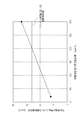
- FIG. 2 is a graph showing the relationship between the linear expansion coefficient on the surface of the external electrode 2 obtained using the simulation method and the linear expansion coefficient of the conductive resin 20.
- the linear expansion coefficient of the conductive resin 20 is changed in the range of 20 to 300 ppm / K
- the linear expansion coefficient on the surface of the external electrode 2 joined to the mounting substrate by soldering is 12 to 34 ppm / K. It varies in the range.
- the linear expansion coefficient on the surface of the solder is 26 ppm / K and the linear expansion coefficient of the conductive resin 20 is 200 ppm / K
- the linear expansion coefficient on the surface of the external electrode 2 joined with the mounting substrate by soldering is 26 ppm / K, which coincides with the linear expansion coefficient on the solder surface.
- the degree of coincidence of the linear expansion coefficients may be within a range of ⁇ 30%.
- the linear expansion coefficient on the surface of the solder is 26 ppm / K
- the linear expansion coefficient on the surface of the external electrode 2 may be designed to be in the range of 18 to 34 ppm / K.
- the value of the linear expansion coefficient can be designed intentionally.
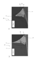
- FIG. 3 is a schematic diagram illustrating a simulation result when a heating / cooling temperature cycle test is performed on the ceramic electronic component 10 according to the embodiment of the present invention using a simulation method.
- the simulation result shown in FIG. 3A shows the simulation result when the ceramic electronic component 10 is subjected to a heating / cooling temperature cycle test of 3814 cycles.
- the ceramic electronic component 10 is a wire on the surface of the external electrode 2 bonded to the mounting substrate 5 and the solder 4 when the Young's modulus of the conductive resin 20 is 1 GPa and the linear expansion coefficient of the conductive resin 20 is 200 ppm / K.
- the expansion coefficient coincides with the linear expansion coefficient on the surface of the solder 4.
- a mesh used in the finite element method is illustrated for the ceramic electronic component 10 to which the external electrode 2 is bonded by the mounting substrate 5 and the solder 4, and a heating / cooling temperature cycle test of 3814 cycles is performed. Even so, there is no change in the mesh of the portion 40 where the external electrode 2 and the solder 4 are joined, and no crack is generated in the direction indicated by the arrow.
- the simulation result shown in FIG. 3B shows the simulation result when the heating / cooling temperature cycle test of 3950 cycles is performed on the ceramic electronic component 10.
- the ceramic electronic component 10 is a wire on the surface of the external electrode 2 bonded to the mounting substrate 5 and the solder 4 when the Young's modulus of the conductive resin 20 is 10 GPa and the linear expansion coefficient of the conductive resin 20 is 26 ppm / K. The expansion coefficient does not match the linear expansion coefficient on the surface of the solder 4.
- a mesh used in the finite element method is illustrated for the ceramic electronic component 10 to which the external electrode 2 is bonded by the mounting substrate 5 and the solder 4, and a heating and cooling temperature cycle test of 3950 cycles is performed. Further, there is a change in the mesh of the portion 40 where the external electrode 2 and the solder 4 are joined, and a crack 41 is generated in the direction indicated by the arrow.
- the ceramic electronic component 10 in which the linear expansion coefficient on the surface of the external electrode 2 bonded to the mounting substrate 5 and the solder 4 matches the linear expansion coefficient on the surface of the solder 4 is bonded to the mounting substrate 5 and the solder 4.
- the linear expansion coefficient on the surface of the external electrode 2 to be applied is gradually increased with an increase in the number of cycles even if the crack 41 occurs, compared with the ceramic electronic component 10 that does not match the linear expansion coefficient on the surface of the solder 4.
- the ceramic electronic component 10 is designed so that the linear expansion coefficient of the surface of the external electrode 2 joined by the solder 4 with the mounting substrate 5 of the ceramic electronic component 10 matches the linear expansion coefficient of the interface (surface) of the solder 4. As a result, the reliability of bonding between the external electrode 2 and the solder 4 is increased.
- FIG. 4 is a schematic diagram showing a simulation result when a heating / cooling temperature cycle test is performed on another ceramic electronic component 11 according to the embodiment of the present invention using a simulation method.
- the simulation result shown in FIG. 4 shows the simulation result when a 3721 cycle heating / cooling temperature cycle test is performed on the ceramic electronic component 11.
- the ceramic electronic component 11 is an external electrode bonded to the mounting substrate (other substrate) 5 by solder 4 when the Young's modulus of the conductive resin 20 is 19 GPa and the linear expansion coefficient of the conductive resin 20 is 177 ppm / K.
- the linear expansion coefficient on the surface of 2 coincides with the linear expansion coefficient on the surface of the solder 4.
- the mesh used in the finite element method is illustrated in the ceramic electronic component 11 in which the external electrode 2 is joined by the mounting substrate 5 and the solder 4, and a heating / cooling temperature cycle test of 3721 cycles is performed. Even so, there is no change in the mesh of the portion 40 where the external electrode 2 and the solder 4 are joined, and the crack 41 does not occur in the direction indicated by the arrow.
- FIG. 5 shows the linear expansion coefficient on the surface of the external electrode 2 and the number of cycles at which the portion 40 where the external electrode 2 and the solder 4 are joined breaks when the heating / cooling temperature cycle test is performed using the simulation method. It is a graph which shows a relationship.
- FIG. 5 shows a case where the heating / cooling temperature cycle test is performed on the ceramic electronic component 11 having the Young's modulus of the conductive resin 20 of 1 GPa and the case of the ceramic electronic component 10 having the Young's modulus of the conductive resin 20 of 19 GPa. The case where the heating / cooling temperature cycle test is performed is shown.
- the linear expansion coefficient on the surface of the external electrode 2 is changed in the range of 11 to 47 ppm / K.
- the number of cycles at which the portion 40 where the external electrode 2 and the solder 4 are joined is broken by the crack 41 is shown.
- the coefficient of linear expansion on the surface of the external electrode 2 is changed in the range of 14 to 29 ppm / K, the number of cycles becomes 12,000 cycles or more, and the number of cycles with respect to the change of the coefficient of linear expansion on the surface of the external electrode 2 is high. .
- the linear expansion coefficient on the surface of the external electrode 2 was changed in the range of 10 to 34 ppm / K.
- the number of cycles at which the portion 40 where the external electrode 2 and the solder 4 are joined is broken by the crack 41 is shown.
- the linear expansion coefficient on the surface of the external electrode 2 is changed in a range of 17 to 24 ppm / K, the number of cycles becomes 11,000 or more, and the number of cycles with respect to the change of the linear expansion coefficient on the surface of the external electrode 2 is high. .
- the Young's modulus of the conductive resin 20 when the heating / cooling temperature cycle test is performed As the Young's modulus of the conductive resin 20 when the heating / cooling temperature cycle test is performed, the number of cycles in which the portion 40 where the external electrode 2 and the solder 4 are joined breaks by the crack 41 becomes 11000 cycles or more. The range in which the linear expansion coefficient on the surface of the conductive resin 20 is changed is widened. Therefore, the external electrode 2 and the solder until the number of cycles when the heating / cooling temperature cycle test is performed on the ceramic electronic components 10 and 11 having a Young's modulus of the conductive resin 20 of 1 GPa or more and 19 GPa or less reaches 11000 cycles or more.
- the range of changing the linear expansion coefficient on the surface of the external electrode 2 joined by the mounting substrate 5 and the solder 4 is 17 ppm / K or more, It is necessary to make it 24 ppm / K or less.
- the conductive resin 20 formed by dispersing conductive powders such as Ag and Cu in a thermosetting resin such as an epoxy resin, a phenol resin, and an acrylic resin is, for example, an imidazole catalyst (0.4% by weight).
- Novolak phenol 1.6 wt%), bisphenol A type epoxy (6.0 wt%), polycarboxylic acid dispersant (1.0 wt%), Ag powder (91.0 wt%) It is. Therefore, among the components of the conductive resin 20, by adjusting the amount of novolac phenol and bisphenol A type epoxy while keeping the ratio of novolak phenol and bisphenol A type epoxy constant, the Young's modulus of the conductive resin 20, The linear expansion coefficient can be changed.
- the external electrode 2 includes the conductive resin 20, and the surface of the external electrode 2 that is joined to the mounting substrate 5 by the solder 4. Since the Young's modulus and the linear expansion coefficient in the conductive resin 20 are determined so that the linear expansion coefficient at the surface of the solder 4 matches the linear expansion coefficient at the surface of the solder 4, By following the surface of the solder 4 that repeats expansion and contraction, the surface of the external electrode 2 joined by the mounting substrate 5 and the solder 4 repeats thermal expansion and contraction in the same manner. Since the crack 41 does not occur in the portion 40 where the solder 4 is joined, or even if the crack 41 occurs, the reliability gradually increases as the number of cycles increases. Kunar.
Landscapes
- Engineering & Computer Science (AREA)
- Microelectronics & Electronic Packaging (AREA)
- Physics & Mathematics (AREA)
- Electromagnetism (AREA)
- Ceramic Capacitors (AREA)
- Electric Connection Of Electric Components To Printed Circuits (AREA)
Abstract
本発明は、加熱冷却温度サイクル試験を行った場合であっても、外部電極とハンダとが接合する部分にクラックが生じない、又は生じたクラックが緩やかに大きくなるセラミック電子部品、及びセラミック電子部品の設計方法を提供する。 本発明は、セラミック焼結体1と、セラミック焼結体1の外側に形成され、導電性樹脂20を含む外部電極2とを備えるセラミック電子部品10である。外部電極2は、下地電極3と、導電性樹脂20と、メッキ6により構成され、実装基板(他の基板)とハンダで接合される外部電極2の表面における線膨張係数と、ハンダの表面における線膨張係数とが一致している。
Description
本発明は、セラミック焼結体の外側に外部電極が形成されたセラミック電子部品、及び該セラミック電子部品の設計方法に関する。
特許文献1に開示してあるセラミック電子部品は、セラミック焼結体と、セラミック焼結体の外側に形成された外部電極とを備え、外部電極は、外部からの衝撃又は熱膨張差を緩衝及び吸収する導電性樹脂で形成されている。また、特許文献1では、セラミック電子部品をハンダで実装基板に接合し、実装基板に接合したセラミック電子部品を所定の高さから繰り返し落下させて、セラミック電子部品のクラックの発生率を評価している。
特許文献1に開示してあるセラミック電子部品では、外部電極を形成する導電性樹脂におけるヤング率を小さくする(導電性樹脂を柔らかくする)ことで、セラミック電子部品を所定の高さから落下させた場合であっても、セラミック電子部品のクラックの発生率が低くなることが示されている。しかし、特許文献1に開示してあるセラミック電子部品に対して、加熱冷却温度サイクル試験を行った場合、外部電極を形成する導電性樹脂のヤング率を小さくしたときでも、外部電極とハンダとが接合する部分にクラックが生じ、生じたクラックがサイクル数の増加とともに大きくなるので、外部電極とハンダとの接合の信頼性が低いという問題があった。
本発明は斯かる事情に鑑みてなされたものであり、加熱冷却温度サイクル試験を行った場合であっても、外部電極とハンダとが接合する部分にクラックが生じない、又は生じたクラックが緩やかに大きくなるセラミック電子部品、及びセラミック電子部品の設計方法を提供することを目的とする。
上記目的を達成するために本発明に係るセラミック電子部品は、セラミック焼結体と、該セラミック焼結体の外側に形成され、導電性樹脂を含む外部電極とを備えるセラミック電子部品であって、他の基板とハンダで接合される前記外部電極の表面における線膨張係数と、前記ハンダの表面における線膨張係数とが一致していることを特徴とする。
上記構成では、導電性樹脂を含み、他の基板とハンダで接合される外部電極の表面における線膨張係数と、ハンダの表面における線膨張係数とが一致しているので、加熱冷却温度サイクル試験を行った場合、熱膨張と熱収縮とを繰り返すハンダの表面に追従して、他の基板とハンダで接合される外部電極の表面も同様に熱膨張と熱収縮とを繰り返すことにより、外部電極とハンダとが接合する部分にクラックが生じない、又はクラックが生じてもサイクル数の増加とともに緩やかに大きくなるため外部電極とハンダとの接合の信頼性が高くなる。
また、本発明に係るセラミック電子部品は、他の基板とハンダで接合される前記導電性樹脂のヤング率が、1GPa以上、19GPa以下の範囲で、他の基板とハンダで接合される前記外部電極の表面における線膨張係数が、17ppm/K以上、24ppm/K以下の範囲であることが好ましい。
上記構成では、他の基板とハンダで接合される外部電極に含まれる導電性樹脂のヤング率が、1GPa以上、19GPa以下の範囲で、他の基板とハンダで接合される外部電極の表面における線膨張係数が、17ppm/K以上、24ppm/K以下の範囲であるので、加熱冷却温度サイクル試験を行った場合、熱膨張と熱収縮とを繰り返すハンダの表面に追従して、他の基板とハンダで接合される外部電極の表面も同じように熱膨張と熱収縮とを繰り返すことができる。
次に、上記目的を達成するために本発明に係るセラミック電子部品の設計方法は、セラミック焼結体と、該セラミック焼結体の外側に形成され、導電性樹脂を含む外部電極とを備えるセラミック電子部品を設計する方法であって、他の基板とハンダで接合される前記外部電極の表面における線膨張係数と、前記ハンダの表面における線膨張係数とが一致するように、前記導電性樹脂におけるヤング率及び線膨張係数を決定することを特徴とする。
上記構成では、導電性樹脂を含み、他の基板とハンダで接合される外部電極の表面における線膨張係数と、ハンダの表面における線膨張係数とが一致するように、導電性樹脂におけるヤング率及び線膨張係数を決定するので、加熱冷却温度サイクル試験を行った場合、熱膨張と熱収縮とを繰り返すハンダの表面に追従して、他の基板とハンダで接合される外部電極の表面も同様に熱膨張と熱収縮とを繰り返すことにより、外部電極とハンダとが接合する部分にクラックが生じない、又はクラックが生じてもサイクル数の増加とともに緩やかに大きくなるため外部電極とハンダとの接合の信頼性が高いセラミック電子部品を設計することができる。
本発明に係るセラミック電子部品では、導電性樹脂を含み、他の基板とハンダで接合される外部電極の表面における線膨張係数と、ハンダの表面における線膨張係数とが一致しているので、加熱冷却温度サイクル試験を行った場合、熱膨張と熱収縮とを繰り返すハンダの表面に追従して、他の基板とハンダで接合される外部電極の表面も同様に熱膨張と熱収縮とを繰り返すことにより、外部電極とハンダとが接合する部分にクラックが生じない、又はクラックが生じてもサイクル数の増加とともに緩やかに大きくなるため外部電極とハンダとの接合の信頼性が高くなる。
本発明に係るセラミック電子部品の設計方法では、導電性樹脂を含み、他の基板とハンダで接合される外部電極の表面における線膨張係数と、ハンダの表面における線膨張係数とが一致するように、導電性樹脂におけるヤング率及び線膨張係数を決定するので、加熱冷却温度サイクル試験を行った場合、熱膨張と熱収縮とを繰り返すハンダの表面に追従して、他の基板とハンダで接合される外部電極の表面も同様に熱膨張と熱収縮とを繰り返すことにより、外部電極とハンダとが接合する部分にクラックが生じない、又はクラックが生じてもサイクル数の増加とともに緩やかに大きくなるため外部電極とハンダとの接合の信頼性が高いセラミック電子部品を設計することができる。
以下、本発明の実施の形態について、図面を参照しながら詳細に説明する。
図1は、本発明の実施の形態に係るセラミック電子部品の構成を示す概略図である。図1に示すように、セラミック電子部品10は、セラミック焼結体1、セラミック焼結体1の外側に形成された外部電極2を備えている。セラミック電子部品10は、例えばチップ型積層コンデンサ、チップ抵抗器等である。
セラミック焼結体1は、チタン酸バリウム等の誘電体セラミックスからなり、内部に図示しない内部電極が形成されている。内部電極は、セラミック層を介して重なり合うように配置されており、セラミック焼結体1の側面から一部が露出している。
外部電極2は、内部電極の一部が側面から露出しているセラミック焼結体1の外側に形成され、内部電極と電気的に接続してある。外部電極2は導電性樹脂20を含み、厚みが20~150μmになるよう形成されている。導電性樹脂20は、エポキシ樹脂、フェノール樹脂、アクリル樹脂等の熱硬化性樹脂に、Ag、Cu等の導電性粉末を分散させて形成している。なお、セラミック電子部品10では、セラミック焼結体1の外側に形成された外部電極2を強固に密着させるため、セラミック焼結体1の表面と導電性樹脂20との間に下地電極3を形成してある。下地電極3は、Ag、Ag-Pd、Cu等の金属粉末を成分とする導電ペーストを塗布し、焼き付けることにより形成されている。導電性樹脂20の外側にはメッキ6が電解メッキにより形成されている。メッキ6としては、Niメッキ、Snメッキ、ハンダメッキ等が挙げられる。本実施の形態における外部電極2は、下地電極3、導電性樹脂20、メッキ6により構成されている。
セラミック電子部品10は、ハンダで外部電極2を、図示していない実装基板(他の基板)に実装して用いられる。そのため、実装基板に実装したセラミック電子部品10は、外部電極2とハンダ4との接合の信頼性を検証するために信頼性試験として、例えば加熱冷却温度サイクル試験を行う。加熱冷却温度サイクル試験は、例えば、セラミック電子部品10を槽内温度が-40度の槽に30分間入れ、次に槽内温度が125度の槽に30分間入れる試験を1サイクルとした信頼性試験である。従来のセラミック電子部品に対して加熱冷却温度サイクル試験を行った場合、外部電極を形成する導電性樹脂のヤング率を小さくして導電性樹脂を柔らかくしたときでも、外部電極とハンダとが接合する部分にクラックが生じ、生じたクラックがサイクル数の増加とともに大きくなり外部電極とハンダとの接合の信頼性が低かった。
そこで、本発明の実施の形態に係るセラミック電子部品10に対して、実装基板とハンダで接合される外部電極2の表面における線膨張係数と、ハンダの表面における線膨張係数とを一致させて、加熱冷却温度サイクル試験を行った場合、熱膨張と熱収縮とを繰り返すハンダの表面に追従して、実装基板とハンダで接合される外部電極2の表面も同じように熱膨張と熱収縮とを繰り返すことにより、外部電極2とハンダとの接合の信頼性を高くできることを考えた。つまり、実装基板とハンダで接合される外部電極2の表面における線膨張係数と、ハンダの表面における線膨張係数とが一致するように、導電性樹脂20の物性(ヤング率、線膨張係数等)を決定し、セラミック電子部品10を設計している。なお、実装基板とハンダで接合される外部電極2の表面における線膨張係数は、外部電極2に含まれる導電性樹脂20の線膨張係数と一致せず、外部電極2の形状、実装基板とハンダで接合する位置等により変動する。
そのため、実装基板とハンダで接合される外部電極2の表面における線膨張係数は、実際にセラミック電子部品10を作成し、作成したセラミック電子部品10に対してデジタル画像相関法等を用いて求める。具体的には、デジタル画像相関法等を用いて、セラミック電子部品10を温度ΔTだけ変化させた場合の、外部電極2の表面における、ある二点間の距離の変化(L1からL2への変化)を測定して、(L2-L1)/ΔT/L1の値から、実装基板とハンダで接合される外部電極2の表面における線膨張係数を求める。ここで、デジタル画像相関法とは、セラミック電子部品10の外部電極2の表面にランダムなパターンを形成し、温度ΔTだけ変化させた場合の前後のセラミック電子部品10を撮影して取得した画像データから、表面に形成されたランダムなパターンを追跡することで熱変形量を測定し、測定した熱変形量に基づいて実装基板とハンダで接合される外部電極2の表面における線膨張係数を求める方法である。
また、実際にセラミック電子部品10を作成することなく、実装基板とハンダで接合される外部電極2の表面における線膨張係数を求める方法として、シミュレーション法がある。シミュレーション法でも、セラミック電子部品10を温度ΔTだけ変化させた場合の、外部電極2の表面における任意の二点間の距離の変化(L1からL2への変化)を測定して、(L2-L1)/ΔT/L1の値から、実装基板とハンダで接合される外部電極2の表面における線膨張係数を求める。
シミュレーション法は、有限要素法を用いてセラミック電子部品10の構造解析を行うことで、実装基板とハンダで接合される外部電極2の表面における線膨張係数を求める方法である。また、シミュレーション法では、セラミック電子部品10をハンダで実装基板に接合した構造の有限要素法モデルを作成し、作成した有限要素法モデルに対して加熱冷却温度サイクル試験を行った場合に、ハンダに生じる非弾性歪み振幅Δεを求めている。さらに、求めた非弾性歪み振幅Δεに、Manson-Coffin則及び線形被害則を適用して、ハンダに蓄積されるダメージを計算し、所定のダメージに達した要素はクラックが生じたとして削除することで、外部電極2とハンダとが接合する部分にクラックが生じる様子等をシミュレーションしている。なお、シミュレーションで計算された破断サイクル数は、実測サンプルの破断サイクル数と比較して補正係数を乗じることで、実際の破断サイクル数とみなすことができる。
以下の説明では、シミュレーション法を用いて、実装基板とハンダで接合される外部電極2の表面における線膨張係数を求める場合について説明する。なお、本発明は、実装基板とハンダで接合される外部電極2の表面における線膨張係数を求める場合に限定されるものではない。図2は、シミュレーション法を用いて求めた外部電極2の表面における線膨張係数と、導電性樹脂20の線膨張係数との関係を示すグラフである。図2においては、導電性樹脂20の線膨張係数を20~300ppm/Kの範囲で変化させた場合、実装基板とハンダで接合される外部電極2の表面における線膨張係数は12~34ppm/Kの範囲で変化する。ここで、ハンダの表面における線膨張係数を26ppm/Kとし、導電性樹脂20の線膨張係数を200ppm/Kとした場合、実装基板とハンダで接合される外部電極2の表面における線膨張係数が26ppm/Kとなり、ハンダの表面における線膨張係数と一致する。線膨張係数の一致度合は、±30%の範囲であれば良い。例えば、ハンダの表面における線膨張係数を26ppm/Kとした場合、外部電極2の表面における線膨張係数が18~34ppm/Kの範囲となるように設計すれば良い。外部電極2に導電性樹脂20を含むことにより、線膨張係数の値の設計を意図的に行うことができる。
次に、導電性樹脂20の線膨張係数を200ppm/Kとして、実装基板(他の基板)とハンダで接合される外部電極2の表面における線膨張係数(26ppm/K)が、ハンダの線膨張係数と一致しているセラミック電子部品10に対して加熱冷却温度サイクル試験を行った場合の結果について、シミュレーション法を用いて説明する。図3は、本発明の実施の形態に係るセラミック電子部品10に対して、シミュレーション法を用いて加熱冷却温度サイクル試験を行った場合のシミュレーション結果を示す概略図である。図3(a)に示すシミュレーション結果は、セラミック電子部品10に対して、3814サイクルの加熱冷却温度サイクル試験を行った場合のシミュレーション結果を示している。セラミック電子部品10は、導電性樹脂20のヤング率を1GPa、導電性樹脂20の線膨張係数を200ppm/Kとした場合の、実装基板5とハンダ4で接合される外部電極2の表面における線膨張係数が、ハンダ4の表面における線膨張係数と一致している。シミュレーション結果には、実装基板5とハンダ4で外部電極2が接合されているセラミック電子部品10に、有限要素法で用いるメッシュが図示してあり、3814サイクルの加熱冷却温度サイクル試験を行った場合であっても、外部電極2とハンダ4とが接合する部分40のメッシュに変化がなく、矢印で示す方向にクラックが生じていない。
一方、図3(b)に示すシミュレーション結果は、セラミック電子部品10に対して、3950サイクルの加熱冷却温度サイクル試験を行った場合のシミュレーション結果を示している。セラミック電子部品10は、導電性樹脂20のヤング率を10GPa、導電性樹脂20の線膨張係数を26ppm/Kとした場合の、実装基板5とハンダ4で接合される外部電極2の表面における線膨張係数が、ハンダ4の表面における線膨張係数と一致していない。シミュレーション結果には、実装基板5とハンダ4で外部電極2が接合されているセラミック電子部品10に、有限要素法で用いるメッシュが図示してあり、3950サイクルの加熱冷却温度サイクル試験を行った場合に、外部電極2とハンダ4とが接合する部分40のメッシュに変化があり、矢印で示す方向にクラック41が生じている。
また、実装基板5とハンダ4で接合される外部電極2の表面における線膨張係数が、ハンダ4の表面における線膨張係数と一致しているセラミック電子部品10は、実装基板5とハンダ4で接合される外部電極2の表面における線膨張係数が、ハンダ4の表面における線膨張係数と一致していないセラミック電子部品10に比べて、クラック41が生じてもサイクル数の増加とともに緩やかに大きくなる。セラミック電子部品10の実装基板5とハンダ4で接合される外部電極2の表面における線膨張係数とハンダ4の界面(表面)の線膨張係数とが一致するようにセラミック電子部品10を設計することにより、外部電極2とハンダ4との接合の信頼性が高くなる。
次に、図4は、本発明の実施の形態に係る別のセラミック電子部品11に対して、シミュレーション法を用いて加熱冷却温度サイクル試験を行った場合のシミュレーション結果を示す概略図である。図4に示すシミュレーション結果は、セラミック電子部品11に対して、3721サイクルの加熱冷却温度サイクル試験を行った場合のシミュレーション結果を示している。セラミック電子部品11は、導電性樹脂20のヤング率を19GPa、導電性樹脂20の線膨張係数を177ppm/Kとした場合の、実装基板(他の基板)5とハンダ4で接合される外部電極2の表面における線膨張係数が、ハンダ4の表面における線膨張係数と一致している。シミュレーション結果には、実装基板5とハンダ4で外部電極2が接合されているセラミック電子部品11に、有限要素法で用いるメッシュが図示してあり、3721サイクルの加熱冷却温度サイクル試験を行った場合であっても、外部電極2とハンダ4とが接合する部分40のメッシュに変化がなく、矢印で示す方向にクラック41が生じていない。
図5は、シミュレーション法を用いて加熱冷却温度サイクル試験を行った場合の、外部電極2の表面における線膨張係数と、外部電極2とハンダ4とが接合する部分40が破断するサイクル数との関係を示すグラフである。図5には、導電性樹脂20のヤング率が1GPaのセラミック電子部品11に対して加熱冷却温度サイクル試験を行った場合と、導電性樹脂20のヤング率が19GPaのセラミック電子部品10に対して加熱冷却温度サイクル試験を行った場合とを示している。導電性樹脂20のヤング率が1GPaのセラミック電子部品11に対して加熱冷却温度サイクル試験を行った場合、外部電極2の表面における線膨張係数を11~47ppm/Kの範囲で変化させたときの、外部電極2とハンダ4とが接合する部分40がクラック41により破断するサイクル数を示している。外部電極2の表面における線膨張係数を14~29ppm/Kの範囲で変化させた場合、サイクル数が12000サイクル以上となり、外部電極2の表面における線膨張係数の変化に対するサイクル数が高い値を示す。また、導電性樹脂20のヤング率が19GPaのセラミック電子部品10に対して加熱冷却温度サイクル試験を行った場合、外部電極2の表面における線膨張係数を10~34ppm/Kの範囲で変化させたときの、外部電極2とハンダ4とが接合する部分40がクラック41により破断するサイクル数を示している。外部電極2の表面における線膨張係数を17~24ppm/Kの範囲で変化させた場合、サイクル数が11000サイクル以上となり、外部電極2の表面における線膨張係数の変化に対するサイクル数が高い値を示す。
加熱冷却温度サイクル試験を行った場合の、導電性樹脂20のヤング率が小さくなるに従って、外部電極2とハンダ4とが接合する部分40がクラック41により破断するサイクル数が11000サイクル以上となり、導電性樹脂20の表面における線膨張係数を変化させる範囲は広くなる。そのため、導電性樹脂20のヤング率が1GPa以上、19GPa以下のセラミック電子部品10、11に対して、加熱冷却温度サイクル試験を行った場合のサイクル数が11000サイクル以上となるまで外部電極2とハンダ4とが接合する部分40がクラック41により破断しないようにするためには、実装基板5とハンダ4で接合される外部電極2の表面における線膨張係数を変化させる範囲を、17ppm/K以上、24ppm/K以下にする必要がある。
エポキシ樹脂、フェノール樹脂、アクリル樹脂等の熱硬化性樹脂に、Ag、Cu等の導電性粉末を分散させて形成されている導電性樹脂20は、例えば、イミダゾール系触媒(0.4重量%)、ノボラックフェノール(1.6重量%)、ビスフェノールA型エポキシ(6.0重量%)、ポリカルボン酸系分散剤(1.0重量%)、Ag粉末(91.0重量%)が成分として含まれている。そのため、導電性樹脂20の成分のうち、ノボラックフェノールとビスフェノールA型エポキシとの比率を一定にしたまま、ノボラックフェノール及びビスフェノールA型エポキシの量を調整することで、導電性樹脂20のヤング率、線膨張係数を変更することができる。
以上のように、本発明の実施の形態に係るセラミック電子部品10、11は、外部電極2は導電性樹脂20を含んで形成され、実装基板5とハンダ4で接合される外部電極2の表面における線膨張係数と、ハンダ4の表面における線膨張係数とが一致するように、導電性樹脂20におけるヤング率及び線膨張係数を決定しているので、加熱冷却温度サイクル試験を行った場合、熱膨張と熱収縮とを繰り返すハンダ4の表面に追従して、実装基板5とハンダ4で接合される外部電極2の表面も同じように熱膨張と熱収縮とを繰り返すことにより、外部電極2とハンダ4とが接合する部分40にクラック41が生じない、又はクラック41が生じてもサイクル数の増加とともに緩やかに大きくなるため外部電極2とハンダ4との接合の信頼性が高くなる。
1 セラミック焼結体
2 外部電極
3 下地電極
4 ハンダ
5 実装基板
6 メッキ
10、11 セラミック電子部品
20 導電性樹脂
41 クラック
2 外部電極
3 下地電極
4 ハンダ
5 実装基板
6 メッキ
10、11 セラミック電子部品
20 導電性樹脂
41 クラック
Claims (3)
- セラミック焼結体と、
該セラミック焼結体の外側に形成され、導電性樹脂を含む外部電極と
を備えるセラミック電子部品であって、
他の基板とハンダで接合される前記外部電極の表面における線膨張係数と、前記ハンダの表面における線膨張係数とが一致していることを特徴とするセラミック電子部品。 - 他の基板とハンダで接合される前記導電性樹脂のヤング率が、1GPa以上、19GPa以下の範囲で、他の基板とハンダで接合される前記外部電極の表面における線膨張係数が、17ppm/K以上、24ppm/K以下の範囲であることを特徴とする請求項1に記載のセラミック電子部品。
- セラミック焼結体と、
該セラミック焼結体の外側に形成され、導電性樹脂を含む外部電極と
を備えるセラミック電子部品を設計する方法であって、
他の基板とハンダで接合される前記外部電極の表面における線膨張係数と、前記ハンダの表面における線膨張係数とが一致するように、前記導電性樹脂におけるヤング率及び線膨張係数を決定することを特徴とするセラミック電子部品の設計方法。
Priority Applications (1)
| Application Number | Priority Date | Filing Date | Title |
|---|---|---|---|
| JP2013500928A JPWO2012114818A1 (ja) | 2011-02-23 | 2012-01-26 | セラミック電子部品、及びセラミック電子部品の設計方法 |
Applications Claiming Priority (2)
| Application Number | Priority Date | Filing Date | Title |
|---|---|---|---|
| JP2011036636 | 2011-02-23 | ||
| JP2011-036636 | 2011-02-23 |
Publications (1)
| Publication Number | Publication Date |
|---|---|
| WO2012114818A1 true WO2012114818A1 (ja) | 2012-08-30 |
Family
ID=46720606
Family Applications (1)
| Application Number | Title | Priority Date | Filing Date |
|---|---|---|---|
| PCT/JP2012/051592 Ceased WO2012114818A1 (ja) | 2011-02-23 | 2012-01-26 | セラミック電子部品、及びセラミック電子部品の設計方法 |
Country Status (2)
| Country | Link |
|---|---|
| JP (1) | JPWO2012114818A1 (ja) |
| WO (1) | WO2012114818A1 (ja) |
Cited By (2)
| Publication number | Priority date | Publication date | Assignee | Title |
|---|---|---|---|---|
| JPWO2014038066A1 (ja) * | 2012-09-07 | 2016-08-08 | 三菱電機株式会社 | パワー半導体装置 |
| JP2018190828A (ja) * | 2017-05-03 | 2018-11-29 | Tdk株式会社 | コイル部品 |
Citations (2)
| Publication number | Priority date | Publication date | Assignee | Title |
|---|---|---|---|---|
| JPH02232914A (ja) * | 1989-03-07 | 1990-09-14 | Kyocera Corp | チップ状コンデンサ |
| JPH11219849A (ja) * | 1998-01-30 | 1999-08-10 | Kyocera Corp | 積層セラミックコンデンサ |
-
2012
- 2012-01-26 WO PCT/JP2012/051592 patent/WO2012114818A1/ja not_active Ceased
- 2012-01-26 JP JP2013500928A patent/JPWO2012114818A1/ja active Pending
Patent Citations (2)
| Publication number | Priority date | Publication date | Assignee | Title |
|---|---|---|---|---|
| JPH02232914A (ja) * | 1989-03-07 | 1990-09-14 | Kyocera Corp | チップ状コンデンサ |
| JPH11219849A (ja) * | 1998-01-30 | 1999-08-10 | Kyocera Corp | 積層セラミックコンデンサ |
Cited By (2)
| Publication number | Priority date | Publication date | Assignee | Title |
|---|---|---|---|---|
| JPWO2014038066A1 (ja) * | 2012-09-07 | 2016-08-08 | 三菱電機株式会社 | パワー半導体装置 |
| JP2018190828A (ja) * | 2017-05-03 | 2018-11-29 | Tdk株式会社 | コイル部品 |
Also Published As
| Publication number | Publication date |
|---|---|
| JPWO2012114818A1 (ja) | 2014-07-07 |
Similar Documents
| Publication | Publication Date | Title |
|---|---|---|
| JP7030730B2 (ja) | セラミック素子およびセラミック素子の製造方法 | |
| JP5172818B2 (ja) | セラミックス電子部品 | |
| JP6106009B2 (ja) | セラミック電子部品 | |
| US8284005B2 (en) | Inductive component and method for manufacturing the same | |
| JP6011574B2 (ja) | 積層セラミックコンデンサ | |
| JP6286914B2 (ja) | セラミック電子部品 | |
| KR20190059972A (ko) | 칩형 전자 부품 | |
| JP2019009129A (ja) | 異方導電性フィルム及び接続構造体 | |
| JP2013069713A (ja) | チップ型電子部品及びチップ型電子部品の製造方法 | |
| US7656677B2 (en) | Multilayer electronic component and structure for mounting multilayer electronic component | |
| JP2013118357A (ja) | セラミック電子部品及びその製造方法 | |
| JP2004266074A (ja) | 配線基板 | |
| JP3267067B2 (ja) | セラミック電子部品 | |
| JP6255742B2 (ja) | 金属端子付きセラミック電子部品 | |
| JP6830314B2 (ja) | 電子部品及び電子部品の実装構造体 | |
| JP2019117899A (ja) | 積層電子部品 | |
| JP2009170706A (ja) | 積層電子部品 | |
| WO2012114818A1 (ja) | セラミック電子部品、及びセラミック電子部品の設計方法 | |
| CN106797701A (zh) | 具有连接元件的电子的器件 | |
| US10952314B2 (en) | Removal of high stress zones in electronic assemblies | |
| JP2008177506A (ja) | 電子部品実装方法及びこれを用いた電子部品実装基板 | |
| CN105702432A (zh) | 电子组件以及具有该电子组件的板 | |
| JP2004146655A (ja) | コイル部品及びそれを利用した回路装置 | |
| JP4952766B2 (ja) | 電子部品及び電子部品の製造方法 | |
| JP2017130561A (ja) | 抵抗器 |
Legal Events
| Date | Code | Title | Description |
|---|---|---|---|
| 121 | Ep: the epo has been informed by wipo that ep was designated in this application |
Ref document number: 12749360 Country of ref document: EP Kind code of ref document: A1 |
|
| ENP | Entry into the national phase |
Ref document number: 2013500928 Country of ref document: JP Kind code of ref document: A |
|
| NENP | Non-entry into the national phase |
Ref country code: DE |
|
| 122 | Ep: pct application non-entry in european phase |
Ref document number: 12749360 Country of ref document: EP Kind code of ref document: A1 |