WO2012114537A1 - 物体検知システム - Google Patents
物体検知システム Download PDFInfo
- Publication number
- WO2012114537A1 WO2012114537A1 PCT/JP2011/056442 JP2011056442W WO2012114537A1 WO 2012114537 A1 WO2012114537 A1 WO 2012114537A1 JP 2011056442 W JP2011056442 W JP 2011056442W WO 2012114537 A1 WO2012114537 A1 WO 2012114537A1
- Authority
- WO
- WIPO (PCT)
- Prior art keywords
- processing
- sensor
- schedule information
- master device
- detection
- Prior art date
- Legal status (The legal status is an assumption and is not a legal conclusion. Google has not performed a legal analysis and makes no representation as to the accuracy of the status listed.)
- Ceased
Links
Images


Classifications
-
- G—PHYSICS
- G01—MEASURING; TESTING
- G01V—GEOPHYSICS; GRAVITATIONAL MEASUREMENTS; DETECTING MASSES OR OBJECTS; TAGS
- G01V8/00—Prospecting or detecting by optical means
- G01V8/10—Detecting, e.g. by using light barriers
- G01V8/20—Detecting, e.g. by using light barriers using multiple transmitters or receivers
-
- H—ELECTRICITY
- H03—ELECTRONIC CIRCUITRY
- H03K—PULSE TECHNIQUE
- H03K17/00—Electronic switching or gating, i.e. not by contact-making and –breaking
- H03K17/94—Electronic switching or gating, i.e. not by contact-making and –breaking characterised by the way in which the control signals are generated
- H03K17/941—Electronic switching or gating, i.e. not by contact-making and –breaking characterised by the way in which the control signals are generated using an optical detector
- H03K17/943—Electronic switching or gating, i.e. not by contact-making and –breaking characterised by the way in which the control signals are generated using an optical detector using a plurality of optical emitters or detectors, e.g. keyboard
-
- H—ELECTRICITY
- H03—ELECTRONIC CIRCUITRY
- H03K—PULSE TECHNIQUE
- H03K2217/00—Indexing scheme related to electronic switching or gating, i.e. not by contact-making or -breaking covered by H03K17/00
- H03K2217/94—Indexing scheme related to electronic switching or gating, i.e. not by contact-making or -breaking covered by H03K17/00 characterised by the way in which the control signal is generated
- H03K2217/941—Indexing scheme related to electronic switching or gating, i.e. not by contact-making or -breaking covered by H03K17/00 characterised by the way in which the control signal is generated using an optical detector
- H03K2217/94102—Indexing scheme related to electronic switching or gating, i.e. not by contact-making or -breaking covered by H03K17/00 characterised by the way in which the control signal is generated using an optical detector characterised by the type of activation
- H03K2217/94104—Indexing scheme related to electronic switching or gating, i.e. not by contact-making or -breaking covered by H03K17/00 characterised by the way in which the control signal is generated using an optical detector characterised by the type of activation using a light barrier
-
- H—ELECTRICITY
- H03—ELECTRONIC CIRCUITRY
- H03K—PULSE TECHNIQUE
- H03K2217/00—Indexing scheme related to electronic switching or gating, i.e. not by contact-making or -breaking covered by H03K17/00
- H03K2217/94—Indexing scheme related to electronic switching or gating, i.e. not by contact-making or -breaking covered by H03K17/00 characterised by the way in which the control signal is generated
- H03K2217/941—Indexing scheme related to electronic switching or gating, i.e. not by contact-making or -breaking covered by H03K17/00 characterised by the way in which the control signal is generated using an optical detector
- H03K2217/94114—Optical multi axis
Definitions
- the present invention relates to an object detection system configured such that a projector and a light receiver of a plurality of multi-optical axis photoelectric sensors are connected to each other via a communication line, and detection processing for each of these sensors proceeds in order.
- the multi-optical axis photoelectric sensor may be simply referred to as “sensor”. Further, the projector and the light receiver may be collectively referred to as “apparatus”.
- the multi-optical axis photoelectric sensor is a sensor in which a detection area by a plurality of optical axes is set by arranging a projector having a plurality of optical elements and a light receiver facing each other.
- each optical axis is enabled in order, and detection processing is performed by a method of checking the light incident state for each optical axis.
- the output is turned on (high level) while the detection area is determined not to be shielded by the detection process, and the detection area is shielded. If so, switch the output off.
- various functions are set in the multi-optical axis photoelectric sensor in order to ensure safety while increasing convenience. For example, when the output is turned off, the function maintains the state until a reset input is made based on a predetermined condition (interlock function). If the detection area is shaded under a predetermined condition Function to maintain output on state (muting function and blanking function), function to forcibly switch output to on state when muting function does not work well and output is turned off (override function) and so on. In a conventional multi-optical axis photoelectric sensor, every time a detection process is performed, it is determined whether a condition for enabling a set function is satisfied, and the output is controlled in accordance with the condition being satisfied. (Hereinafter, these processes are collectively referred to as “function processes”).
- a multi-optical axis photoelectric sensor is not limited to being used alone, but a projector and a receiver of a plurality of sensors are connected via a communication line, and detection processing for each sensor proceeds in order based on communication between the sensors.
- a system configured to be configured is constructed.
- Patent Document 2 a sensor at one end of a plurality of sensors connected in series is used as a master sensor, and this master sensor performs a detection process for the first time, and then a lower sensor.
- a detection command is transmitted in order from the upper level to the lower level by transmitting a command instructing the start of detection to each sensor and performing the same operation in order.
- the projector and the light receiver of each sensor communicate with upper and lower devices at the time of activation, and determine whether the device is a master or a slave according to the result of each communication. Is described.
- Functional processing and self-diagnosis processing include processing that can be performed by each sensor alone, but these processing are also performed by commands from the master sensor so that they are performed at a timing that does not affect detection processing. The duration of processing is controlled.
- the detection result is transmitted from the sensor of each slave to the master sensor, and the detection result is integrated by the master sensor to determine whether or not the muting condition is satisfied.
- OSSD diagnosis OSSD is an abbreviation of Output Signal Switching Device
- start diagnosis from the master sensor to each slave sensor.
- cutting off the output by each sensor for a very short time cutting off so as not to affect the operation of the circuit receiving the output.
- the control unit of each sensor determines whether or not the output signal has been correctly changed by feedback from the output signal line, and transmits the determination result to the master sensor.
- This invention pays attention to said problem, and makes it a subject to make various processes smoothly progress by each sensor managing the process timing in an own apparatus independently, and to speed up a process.
- the present invention provides an object detection system in which a projector and a light receiver of a plurality of multi-optical axis photoelectric sensors are connected to each other via a communication line, and detection processing for each sensor proceeds in sequence based on communication between the sensors. Applies to In this system, the projector and the light receiver of each multi-optical axis photoelectric sensor are each provided with a timer for managing the operation timing of the device, and one of these devices functions as a master device.
- the master device is based on the relationship between the sensors in the system (number of sensors, connection order of each device, correspondence between the projector and light receiver, etc.) and the number of optical axes of each sensor.
- Schedule setting means for creating schedule information representing a progress schedule with a period for performing processing other than processing
- schedule transmission means for transmitting schedule information to other devices in the system
- Command transmitting means for transmitting a command for requesting the start of processing based on the command.
- Each device other than the master device corrects each timer to synchronize with the master device in response to receiving a command from the master device. Furthermore, each device including the master device performs a process other than the detection process and the storage means for storing the schedule information, the period in which the own apparatus should perform the detection process by referring to the schedule information based on the time measured by the timer And a process execution means for determining a power period and executing a process corresponding to each determined period.
- the projector or the light receiver of any one of the plurality of sensors serves as a master device, and the progress schedule of processing in each device in the system including the self-device is determined and this schedule is shown.
- Each device determines the period for performing detection processing and processing other than detection processing based on this schedule information, and performs each processing without communicating with other sensors. Therefore, it is possible to avoid the occurrence of deficiencies that the detection processes between the sensors overlap or the order of the detection processes is out of order.
- the detection processing in each sensor can be set by setting a schedule so that no other processing is performed when the detection processing order comes around. Can proceed smoothly.
- the schedule setting unit of the master device proceeds in order without overlapping the detection processing periods of the sensors, and the processes that can be performed independently by each sensor by processes other than the detection processes.
- Schedule information is generated in parallel with the period in which detection processing is performed by other sensors.
- the schedule setting unit of the master device sets the period for performing the processing that requires communication between the sensors after the detection processing of each sensor is complete for all the devices. Create schedule information.
- each device independently manages the period of processing that requires communication between sensors, such as communication for muting control and OSSD diagnosis, and the timing of the start and end of these processes. Can be unified.
- the command transmission unit of the master device recognizes the circulation cycle of the process defined in the schedule information based on the time measured by the timer of the own device and the schedule information, and the cycle is In response to the elapse of a time corresponding to the period of progress of the predetermined cycle, a command for re-correcting each timer is transmitted to another device. In this transmission, a command having substantially the same content as the command for requesting the start of the first process may be transmitted.
- the schedule setting means of the master device recognizes the relationship between the sensors in the system and the number of optical axes of each sensor by communicating with other devices after activation, and the recognition result. Based on the above, schedule information is created by determining the detection processing timing of each device.
- the schedule transmission means transmits the schedule information to another device in response to the completion of the creation of the schedule information.
- schedule information is created based on the relationship between the sensors in the system and the number of optical axes, and is transmitted to each device, so even if the system configuration is changed, By restarting the device, the schedule information can be updated to the content according to the changed configuration.
- the advance schedule between the detection process period of each sensor and the period for performing the process other than the detection process is determined in advance, and the projector and the light receiver constituting each sensor are operated according to the determined schedule. Even if communication is not performed between devices constituting different sensors, it is possible to proceed with the detection processing in accordance with the order and timing of the detection processing, and to smoothly proceed with processing other than the detection processing. Therefore, the circulation cycle of the detection process is greatly shortened.
- FIG. 1 shows the appearance of a multi-optical axis photoelectric sensor to which the present invention is applied.
- the multi-optical axis photoelectric sensor S of this embodiment is a pair of a light projector 1 and a light receiver 2.
- the projector 1 and the light receiver 2 have a long casing 100 as a main body.
- a plurality of optical elements (the light emitting element 11 in the light projector 1 and the light receiving element 21 in the light receiver 2) and a control board (not shown) are accommodated in each casing 100, respectively.
- a window for allowing light to pass through is formed on the front surface of each housing 100.
- the light emitting element 11 and the light receiving element 21 are arranged so as to be aligned along the longitudinal direction of the housing 100 in a state where the light projecting surface or the light receiving surface is opposed to the window portion.
- the light emitting element 11 and the light receiving element 21 are opposed to each other with a predetermined interval so that the light emitting element 11 and the light receiving element 21 face each other in a one-to-one relationship. P is formed.
- FIG. 2 shows a configuration of main circuits included in the multi-optical axis photoelectric sensor S described above.
- the projector 1 is provided with a drive circuit 12 for each light emitting element 11, an optical axis sequential selection circuit 14, a control circuit 15, a communication circuit 16, a power supply circuit 18, and the like.
- Each light emitting element 11 is connected to a control circuit 15 via a drive circuit 12 and an optical axis sequential selection circuit 14, respectively.
- the light receiver 2 is provided with an amplification circuit 22 and an analog switch 23 for each light receiving element 21, an optical axis sequential selection circuit 24, a control circuit 25, a communication circuit 26, an output circuit 27, and a power supply circuit 28.
- an amplification circuit 201 and an A / D conversion circuit 202 are provided on the transmission line 29 from each analog switch 23 to the control circuit 25.
- the power supply circuits 18 and 28 are supplied with power from the common external power supply 5 and supply power to each circuit in the apparatus.
- the control circuits 15 and 25 include a memory and a timer to be described later, and can communicate with each other via the communication circuits 16 and 26.
- the output circuit 27 includes two output terminals, and the signal lines connected to the respective terminals are connected to a power supply circuit (not shown) of a machine in the dangerous area.
- the control circuits 15 and 25 sequentially switch the optical axes selected by the optical axis sequential selection circuits 14 and 24 one by one from the top to the bottom.
- the control circuit 15 of the projector 1 outputs a lighting control signal in time with the switching of the optical axis selection, and the control circuit 25 of the light receiver 2 applies the optical axis being selected in accordance with the switching of the optical axis selection.
- the corresponding analog switch 23 is turned on.
- the received light amount signal by the light receiving element 21 of the selected optical axis is guided to the transmission line 29, and the received light amount data generated through the amplification by the amplifier circuit 201 and the digital conversion by the A / D conversion circuit 202 is the control circuit. 25.
- the control circuit 25 of the light receiver 2 corresponds to the light emitting element 11 that is turned on each time. Data indicating the amount of light received by the light receiving element 21 is input.
- the control circuit 25 determines whether or not the selected optical axis is shielded by comparing the received light amount data with a predetermined light incident threshold value. Further, every time the selection of the optical axis is completed, the determination results for each optical axis are integrated to determine whether or not the detection area P is shielded from light.
- the detection process is realized by cooperative control of the control circuits 15 and 25 of the projector 1 and the light receiver 2, and is repeated at a predetermined cycle. While it is determined that the detection area P is not shielded from light, a high-level detection signal is output from the output circuit of the light receiver 2, but when it is determined that the detection area P is shielded from light, the detection is detected. The signal is switched to a low level.
- the multi-optical axis photoelectric sensor S may be moved alone, but a plurality of photoelectric sensors S may be connected and moved via the code line 101 and the connecting cord shown in FIG. Figure 3 shows the connection example, the sensor S A in combination with the light receiver 2 A light projector 1 A, a sensor S B in combination with the light projector 1 B and receiver 2 B, the projector 1C receiving between the sensor S C in combination with vessel 2C, the projector other and the light receiver each other are connected. Also, projector 1 A and receiver 2 A located at one end of each connecting member are connected via a cable.
- the control circuit 15 and the communication circuit 16 are provided for the projectors 1 A , 1 B and 1 C
- the control circuit 25, the communication circuit 26 and the output circuit 27 are provided for the light receivers 2 A , 2 B and 2 C.
- the sensors S A , S B , S C , the projectors 1 A , 1 B , 1 C , and the light receivers 2 A , 2 B , 2 C are collectively referred to as “sensor S”, “projector”. 1 ”and“ receiver 2 ”.
- the projector 1 and the light receiver 2 may be collectively referred to as “apparatus”.
- the light projector 1 and the light receiver 2 may or may be arranged along the length direction (vertically arranged), are arranged along the width direction (side by side) In some cases. In some cases, the devices are arranged without being aligned.
- the control circuit 15 between the projectors 1 and the control circuit 25 between the light receivers 2 are connected in series via signal lines (master / slave lines), respectively. Connected. As will be described later, each device recognizes whether it is a master device or a slave device by exchanging signals via this connection.
- the communication circuit 16, 26 of each device is connected to a communication line connected to a loop via the projector 1 A and the light receiver 2 A sensor S A.
- the communication circuits 16 and 26 of each device are connected in series, enabling communication between the projector 1 and the light receiver 2 of each sensor S and between devices belonging to different sensors S. Communication is also possible.
- Each terminal of the output circuit 27 of the light receiving device 2 are connected in series, the output from the light receiver 2 A light receiving circuit 27 is output as the detection signal.
- the power supply circuits 18 and 28 of each device are also connected to a common line from the external power supply 5.
- the control circuit 25 of each light receiver 2 is connected to an output line in order to receive feedback of the state of the detection signal.
- the sensor S photodetector 2 A of A is functioning as the master device, the other sensors S B, the S C projectors 1 B, 1 C and the light receiver 2 B, 2 C, and the sensor S A
- the projector 1A is set as a slave device.
- the projector 1 A sensor S A the ability to manage other projector 1 B, 1 C as a slave device forming the master device and pairs are set.
- the assignment of the master device and slave device and the ranking among the devices are determined by performing the following processing at the time of every hour startup.
- control circuits 15 and 25 of each device when the control circuits 15 and 25 of each device are activated by turning on the power from the common power source, the control circuits 15 and 25 start the process of outputting a pulse signal to the master / slave line above the own device at the same time.
- Each of the control circuits 15 and 25 checks whether or not a pulse signal is input from the master / slave line below the own device while continuing this output. According to the configuration of FIG. 3, the projector 1 A and a pulse signal to the optical receiver 2 A sensor S A is not input, the other devices will receive the input of the pulse signal.
- Recognizing the control circuit 25 of the light receiver 2 A may have that there is no input of the pulse signal and the own device is a master device. Then, the output of the pulse signal is stopped, and communication for assigning an address to the slave device is started.
- the light receiver 2 A master device 2 A in other words the light receiver 2 A master device 2 A.
- the control circuits 25 of the other light receivers 2 B and 2 C recognize that the own device is a slave device when the pulse signal is input. Thereafter, with the input of the pulse signal is stopped, to communicate in response to commands from the master device 2 A, notifying the attributes of its own device to the master device 2 A (such as the type and number of beams of the device), Upon receiving the address notification, this is registered in the memory. In the light receivers 2 B and 2 C that have performed these processes, the output of the pulse signal to the upper master / slave line is stopped.
- the light receiver 2 B that has not received the input of the pulse signal from the master device 2 A first communicates with the master device 2 A, and then the light receiver 2 C performs communication.
- the master device 2 A assign an address to set the order in the order in which it can communicate to each light receiver 2 B, 2 C, correspondence to its address and attributes broadcast from the light receiver 2 B, 2 C And register.
- the control circuit 15 of the projector 1A recognizes that its own device is a slave device paired with the master device when no pulse signal is input. Thereafter, in the same manner as the light receivers 2 B and 2 C , the address is notified in response to the command from the master device 2 A, and the self-device is informed of the projector corresponding to the master device 2 A. .
- the projector 1 A stops the output of the pulse signal, thereafter, according to the instructions of the light receiver 2 A, to the projector 1 B, 1 C lower, the light receiver 2 A light-receiving device 2 B, 2 C
- the same communication as that performed for is performed.
- the projectors 1 B and 1 C recognize the device as a general slave device in response to the input of the pulse signal, and sequentially communicate with the projector 1 A in the same procedure as the light receivers 2 B and 2 C. And receive notification of the address. Information indicating the attributes of the own device is also transmitted from the projectors 2 B and 2 C. These are sent to the master device 2 A via the projector 1 A.
- the light receiver 2 A sensor S A is functioning as the master device receives an instruction of the master device 2 A light projector 1 A to impart a function of managing lower projector 1B, the 1C
- this relationship may be reversed.
- An object detection system using the sensors S A , S B , and S C is constructed by the above connection and communication and recognition processing between the devices.
- the head of the sensor S A top-level, S B, in the order of S C performs the detection process at a timing not overlapping the period of the detection process of the other sensors S.
- the output from the output circuit 27 of the sensor S is turned off. Detection signals are thereby outputted from the master device 2 A also turned off.
- each device performs function processing and self-diagnosis processing in addition to detection processing, as in the past, but communication between sensors is performed by independently managing the period during which each device performs various processing. By minimizing the frequency of these, various processes are smoothly advanced.
- schedule information as shown in FIG. 4 is shared between the devices, and each process proceeds based on the schedule information.
- this schedule information the distribution between the period of detection processing of each device and the period of performing processing (functional processing and self-diagnosis) other than the detection processing is determined.
- FIG. 4 shows two specific examples (1) and (2) for schedule information.
- a sensor having 102 optical axes a sensor having 24 optical axes, and a sensor having 60 optical axes are used. Since the vertical relationship of the sensors is different, different schedule information is set.
- the time axis is set in the direction from the left to the right, and the progress schedule of the processing of each sensor S is compared vertically.
- Each schedule includes a period of function processing and self-diagnosis in addition to a period of detection processing. Also, the white portions in the schedule are waiting periods during which no processing is performed.
- the period of function processing and self-diagnosis is a period of processing (hereinafter referred to as “single function processing and self-diagnosis”) performed independently by one sensor S without communication with other sensors S. It can be divided into periods of processing that require communication between sensors (muting control, OSSD diagnosis, etc., these are hereinafter referred to as “common processing”). In FIG. 4, function processing and self-diagnosis by itself are described as “function processing / self-diagnosis”. In these processes, communication between the sensors is not performed, but communication is appropriately executed between the pair of projectors 1 and light receivers 2 constituting the sensor S.
- the schedule of each sensor S is set so that the periods of the detection processes do not overlap while these periods proceed almost continuously.
- the individual function processing and self-diagnosis processing of each sensor S are performed in parallel with the detection processing of other sensors. Further, when the detection process in each sensor S is completed, the common process is started in all the sensors S all at once.
- the length of the detection processing period of each sensor S increases as the number of optical axes increases.
- the time required for the processing can be made substantially constant. Therefore, in this embodiment, based on the order of detection processing of each sensor S and the length of the detection processing period, individual function processing and self-diagnosis are performed for each sensor based on the length of time before and after the detection processing. Assign a period to set the schedule.
- detection processing period of the sensor S A is shorter than the function process and the time required for the self-diagnosis alone
- the sensor S B performing the detection process in the second
- the detection process The function processing and self-diagnosis period are set separately for the front and the back.
- the sensor S C performing the detection process in the third, the waiting time long enough before the detection process occurs, function processing and the duration of the self-diagnosis alone is set prior to the detection process.
- the function process and the self-diagnosis include a plurality of types of processes, and the actual schedule information determines the execution time for each of these processes.
- Progressive order of the processing may be constant but, as in the example of a sensor S B in FIG. 4 (2), when carrying out the functional processing and self-divides the period before and after the detection process, The order of processing may be changed based on the relationship between the length of each period and the length of time required for various processes.
- the progression order and execution period for a plurality of types of processing are determined, but the definition is unified for all sensors S.
- Schedule information described above is created by the master device 2 A at system startup, it is delivered from the master device 2 A to each slave device.
- the master device 2 A before starting the processing shown in the schedule information, collectively transmits a command signal to determine the start of the process to the slave device.
- Each slave device performs correction for restarting the operation clock of its own timer after a predetermined time from the reception of the command signal, and resets the time measurement. Even the master device 2 A, based on the number of clocks after the transmission of the command signal, resets the time measured by the timer of the self apparatus to suit each device and timing. It should be noted that the time required from the command reception to the correction at each slave device is based on the length of time required for communication between the master device 2A and the slave device at the time of startup.
- the correction timings are set to be synchronized with each other and registered in the memory of each slave device.
- the timing of each device is synchronized by the above processing, and the time measured by each timer is also matched. Therefore, even if communication between the projector 1 and the light receiver 2 that make a pair is not performed, Axis selection timing can be adjusted. In addition, it is possible to prevent the detection processing timing of each sensor S from deviating and overlapping with the detection processing of other sensors S, or the occurrence of inadequacies that cause the detection processing order to be out of order. Even in common processing that requires communication between sensors, the start timing of processing in each sensor S is unified, so that communication errors can be prevented and processing can be performed efficiently within a period.
- the master device 2 A while recognizing the time required for 1 cycle performed all processes defined in the schedule information, each time the time of one cycle has elapsed, the above command Send a signal. However, as long as it can ensure the operation clock accuracy of each device, the master device 2 A is at a time corresponding to progress a predetermined cycle process defined two or more in the schedule information, transmits a command signal You may make it do.
- the master device 2 A is to communicate with each slave device and order attributes of the slave device (or projector 1 or the light receiver 2) recognizes such as the number of optical axes, assigns an address (step ST1). Details of this processing are as described above with reference to FIG.
- step ST2 the correspondence between the projector 1 and the light receiver 2 and the number of sensors S are recognized based on the respective recognition results.
- the master device 2 A uses the detection processing time of the waiting time and the sensors S, each sensor S, sets the start time and end time of the detection process. These times are represented by the time measured by the timer. Further, in this setting, the detection process of each sensor S may be set to be completely continuous, but a slight margin may be provided between the detection processes. Alternatively, the detection processing time of each sensor S may be set slightly longer than the length calculated from the number of optical axes.
- step ST6 for each sensor S, the length of idle time before and after the detection processing period of the sensor is derived, and based on the result, the execution period of the independent function processing and self-diagnosis processing is set.
- a specific start time and end time are determined for each of a plurality of types of processing. Similar to the detection process, these times are also represented by the time measured by the timer.
- the master device 2 A at step ST8, by integrating the result of each setting described above, each sensor S, to create a schedule information indicating the progress schedule of the processing in the sensor.
- Each schedule information is given the addresses of the projector 1 and the light receiver 2 of the corresponding sensor S as index information.
- Master device 2 A stores each schedule information in its own memory in step ST9, further collectively transmitted to each schedule information to the slave device at step ST10. This completes the setting process.
- each device timers including the master device 2 A is reset simultaneously accordingly. Thereafter, each device executes the corresponding process while determining the start time and end time of various processes based on the valid schedule information (schedule information suitable for its own device).
- the description has been made on the assumption that a plurality of sensors S are connected and used. Similarly, when the sensor S is used alone, the light receiver 2 is the master device. Then, schedule information for the own device and the projector 1 is created, and each device independently manages the processing period based on the schedule information.
- each device by recognizing whether each device is a master device or a slave device at the time of starting the system, by performing the setting process shown in FIG. 5 in the master device, Since the schedule information of each device is created and provided to each device, even when the system configuration is changed, the change can be easily handled.
- schedule information stored is created in the memory of each device when power was first introduced are connected each device also stored schedule from the master device 2
- a external New schedule information may be created in response to the input of a signal instructing to update information, and the schedule information of each device may be rewritten with new information.
Landscapes
- Physics & Mathematics (AREA)
- Life Sciences & Earth Sciences (AREA)
- General Life Sciences & Earth Sciences (AREA)
- General Physics & Mathematics (AREA)
- Geophysics (AREA)
- Geophysics And Detection Of Objects (AREA)
- Electronic Switches (AREA)
- Switches Operated By Changes In Physical Conditions (AREA)
Abstract
複数の多光軸光電センサSA,SB,SCを構成する投光器および受光器のうちの1台をマスタ機器とし、その他の機器をスレーブ機器として、マスタ機器において、各センサSA,SB,SCの検出処理の期間および検出処理以外の処理を実施する期間を表すスケジュール情報を作成し、これを各機器のメモリに保存する。各機器はマスタ機器からのコマンドに応じてタイマを一斉に始動し、タイマの計時時間に基づきスケジュール情報を参照して自装置が検出処理を実施すべき期間および検出処理以外の処理を実施すべき期間を判別し、判別した各期間にそれぞれ該当する処理を実施する。
Description
本発明は、複数の多光軸光電センサの投光器および受光器が通信回線を介して相互に接続され、これらのセンサ毎の検出処理が順番に進行するように構成された物体検知システムに関する。
なお、以下では、多光軸光電センサを単に「センサ」という場合がある。また投光器および受光器を総称して「機器」と言う場合がある。
多光軸光電センサは、複数の光学素子を有する投光器と受光器とを対向させて配備することにより、複数の光軸による検知エリアが設定される形態のセンサである。このセンサでは、各光軸を順に有効にして光軸毎に入光状態をチェックする方法による検出処理を実行する。また、安全用途に使用される多光軸センサでは、検出処理により検知エリアが遮光されていないと判定されている間は出力をオン状態(ハイレベル)にし、検知エリアが遮光されていると判定された場合には出力をオフに切り替える。
また多光軸光電センサには、安全性を確保する一方で利便性を高めるために、様々な機能が設定されている。たとえば、出力をオフ状態にしたときに、定められた条件に基づくリセット入力がなされるまでその状態を維持する機能(インターロック機能)、あらかじめ定めた条件下で検知エリアが遮光された場合には出力のオン状態を維持する機能(ミューティング機能やブランキング機能)、ミューティング機能がうまく働かずに出力がオフ状態になったときにその出力を強制的にオン状態に切り替える機能(オーバーライド機能)などがある。従来の多光軸光電センサでは、検出処理を1サイクル実施する毎に、設定されている機能を有効にする条件が成立したか否かの判断や、条件が成立したことに応じて出力を制御する処理などを実行する(以下、これらの処理を「機能処理」と総称する。)。
また多光軸光電センサでは、回路や出力の異常を検出するために、様々な内容の自己診断処理を実施する(特許文献1の段落0016,0017を参照。)。これらの自己診断処理も、検出処理の合間に実施される。
上記の検出処理、機能処理、および自己診断処理はいずれも、投光器と受光器とが通信により動作タイミングを合わせて協働して実施するものである。
多光軸光電センサは単独で使用される場合に限らず、複数のセンサの投光器および受光器を通信回線を介して接続し、センサ間での通信に基づき、センサ毎の検出処理を順番に進行させるように構成されたシステムが構築される場合がある。
具体的な従来例として、特許文献2には、直列に接続された複数のセンサのうちの一端にあるセンサをマスタセンサとして、このマスタセンサが最初に検出処理を実行した後に1つ下位のセンサに検出の開始を指示するコマンドを送信し、以下、各センサが順に同様の動作をすることにより、上位から下位に向けて検出処理を順番に進行させることが記載されている。
また特許文献2には、各センサの投光器および受光器が、起動時に上位および下位の機器と通信し、各通信の結果に応じて自装置がマスタであるか、スレーブであるかを判別することが、記載されている。
特許文献2のように複数のセンサが接続されたシステムでは、センサ間で通信をすることにより、各センサの検出処理を重複することなく順番に進行させるようにしている。
機能処理や自己診断処理には、各センサが単独で実施することが可能な処理もあるが、これらの処理に関しても、検出処理に影響しないタイミングで実施されるように、マスタセンサからのコマンドによって処理の期間が制御される。
さらに機能処理や自己診断処理の中には、センサ間での通信が必須になる処理がある。
たとえば、ミューティングが適用される場合には、各スレーブのセンサからマスタセンサに検出結果を送信し、マスタセンサで各検出結果を統合してミューティングの条件を満たすかどうかを判定する。また各センサからの出力の安全性が確保されているかどうかを調べる診断処理(OSSD診断と呼ばれる。OSSDはOutput Signal Switching Deviceの略である。)では、マスタセンサから各スレーブのセンサに診断の開始を求めるコマンドを送信し、各センサで出力をごく短い期間遮断する処理(出力を受ける回路の動作に影響を与えない程度の遮断)を実施する。各センサの制御部は、出力信号線からのフィードバックにより出力信号が正しく変化したかどうかを判別し、その判別結果をマスタセンサに送信する。
たとえば、ミューティングが適用される場合には、各スレーブのセンサからマスタセンサに検出結果を送信し、マスタセンサで各検出結果を統合してミューティングの条件を満たすかどうかを判定する。また各センサからの出力の安全性が確保されているかどうかを調べる診断処理(OSSD診断と呼ばれる。OSSDはOutput Signal Switching Deviceの略である。)では、マスタセンサから各スレーブのセンサに診断の開始を求めるコマンドを送信し、各センサで出力をごく短い期間遮断する処理(出力を受ける回路の動作に影響を与えない程度の遮断)を実施する。各センサの制御部は、出力信号線からのフィードバックにより出力信号が正しく変化したかどうかを判別し、その判別結果をマスタセンサに送信する。
このように、多光軸光電センサによる従来のシステムでは、センサ間で頻繁に通信をしながら処理を進行させるが、そのために各処理を円滑に進行させるのが困難になり、検出処理の循環サイクルを十分に短縮できないという問題がある。
本発明は上記の問題に着目し、各センサが独立して自装置における処理のタイミングを管理することにより各種処理を円滑に進行させて、処理を高速化することを課題とする。
本発明は、複数の多光軸光電センサの投光器および受光器が通信回線を介して相互に接続されると共に、センサ間での通信に基づき、センサ毎の検出処理を順番に進行させる物体検知システムに適用される。このシステムでは、各多光軸光電センサの投光器および受光器は、それぞれ自装置における動作のタイミングを管理するためのタイマを具備すると共に、これらの機器の中の1台がマスタ機器として機能する。
マスタ機器は、システム内のセンサの関係(センサの数、各機器の連結順序、投光器と受光器との対応関係など)および各センサの光軸数に基づき、各センサの検出処理の期間と検出処理以外の処理を実施する期間との進行スケジュールを表すスケジュール情報を作成するスケジュール設定手段と、システム内の他の機器にそれぞれスケジュール情報を送信するスケジュール送信手段と、他の各機器にスケジュール情報に基づく処理の開始を求めるコマンドを送信するコマンド送信手段とを具備する。
マスタ機器以外の各機器はマスタ機器からのコマンドを受信したことに応じてそれぞれのタイマをマスタ機器に同期するように補正する。さらに、マスタ機器を含む各機器は、スケジュール情報を記憶する記憶手段と、タイマの計時時間に基づきスケジュール情報を参照して自装置が検出処理を実施すべき期間および検出処理以外の処理を実施すべき期間を判別し、判別した各期間にそれぞれ該当する処理を実行する処理実行手段とを、具備する。
上記のシステムによれば、複数のセンサの中のいずれか1センサの投光器または受光器がマスタ機器となって、自装置を含むシステム内の各機器における処理の進行スケジュールを定め、このスケジュールを示すスケジュール情報を各機器に送信する。各機器は、それぞれこのスケジュール情報に基づいて検出処理や検出処理以外の処理を実施する期間を判別し、他のセンサと通信をすることなく各処理を実施するが、各機器のタイマの計時時間が整合しているので、センサ間での検出処理が重なったり、検出処理の順序が狂うような不備が生じるのを回避することができる。また、各機器の検出処理の期間の長さや順番に基づいて、検出処理の順番が廻ってくるときに他の処理を実施することがないようなスケジュールを設定することにより、各センサにおける検出処理をスムーズに進行させることができる。
上記システムの第1の実施形態では、マスタ機器のスケジュール設定手段は、各センサの検出処理の期間が重なることなく順番に進行すると共に、検出処理以外の処理で各センサが単独で実施可能な処理の期間をそれぞれ他のセンサで検出処理が実施されている期間に並列して割り当てたスケジュール情報を作成する。この実施形態によれば、各センサにおける検出処理の循環周期が短縮されると共に、それぞれのセンサにおいて検出処理を実施していない期間に、検出処理以外の自装置で単独で実施可能な処理を、マスタ機器からの指示を受けずに自主的に実施することができる。よって処理の効率を大幅に向上することができる。
上記システムの第2の実施形態では、マスタ機器のスケジュール設定手段は、各センサの検出処理が一巡した後にセンサ間での通信が必要な処理を実施する期間が全ての機器に統一して設定されたスケジュール情報を作成する。この実施形態によれば、ミューティング制御のための通信やOSSD診断など、センサ間での通信が必要な処理の期間を各機器で独自に管理すると共に、これらの処理の開始や終了のタイミングを統一することができる。
上記システムの第3の実施形態では、マスタ機器のコマンド送信手段は、自装置のタイマによる計時時間とスケジュール情報とに基づき、スケジュール情報に定義された処理の循環周期を認識しつつ、当該周期が所定サイクル進行する期間に相当する時間が経過したことに応じて、他の機器にそれぞれのタイマを再補正することを求めるコマンドを送信する。なお、この送信では、最初の処理の開始を求めるコマンドと実質的に同内容のコマンドを送信してもよい。
この実施形態によれば、各機器のタイマの計時動作のずれが定期的に補正されるので、計時時間の整合性が保たれ、各機器における処理を正しく進行させることが可能になる。
上記システムの第4の実施形態では、マスタ機器のスケジュール設定手段は、起動後に他の機器と通信を行うことにより、システム内のセンサの関係および各センサの光軸数を認識し、その認識結果に基づき各機器の検出処理のタイミングを定めてスケジュール情報を作成する。スケジュール送信手段は、スケジュール情報の作成が完了したことに応じて当該スケジュール情報を他の機器に送信する。
この実施形態によれば、システムが起動する都度、システム内のセンサの関係や光軸数に基づきスケジュール情報が作成され、各機器に送信されるので、システムの構成が変更された場合でも、各機器を再起動させることによって、スケジュール情報を変更後の構成に応じた内容に更新することができる。
本発明によれば、あらかじめ各センサの検出処理の期間と検出処理以外の処理を実施する期間との進行スケジュールを定め、各センサを構成する投光器および受光器を定められたスケジュールに従って動作させることにより、異なるセンサを構成する機器の間で通信を行わなくとも、検出処理の順序やタイミングを守って検出処理を進行させ、検出処理以外の処理も円滑に進行させることが可能になる。よって、検出処理の循環サイクルが大幅に短縮される。
図1は、本発明が適用される多光軸光電センサの外観を示す。
この実施例の多光軸光電センサSは、投光器1と受光器2とを対にしたものである。投光器1および受光器2は長尺状の筐体100を本体とする。各筐体100の内部には、それぞれ複数の光学素子(投光器1では発光素子11、受光器2では受光素子21)や制御基板(図示せず。)が収容される。
この実施例の多光軸光電センサSは、投光器1と受光器2とを対にしたものである。投光器1および受光器2は長尺状の筐体100を本体とする。各筐体100の内部には、それぞれ複数の光学素子(投光器1では発光素子11、受光器2では受光素子21)や制御基板(図示せず。)が収容される。
各筐体100の前面には、光を通過させるための窓部が形成されている。発光素子11および受光素子21は、投光面または受光面を窓部に対向させた状態で、筐体100の長手方向に沿って整列するように配置される。これらの発光素子11と受光素子21とが一対一の関係で対向するように投光器1と受光器2と所定の間隔を隔てて対向配備することにより、両者の間に複数の光軸による検知エリアPが形成される。
図2は、上記の多光軸光電センサSに含まれる主要な回路の構成を示す。
投光器1には、発光素子11のほか、発光素子11毎の駆動回路12、光軸順次選択回路14、制御回路15、通信回路16、電源回路18などが設けられる。各発光素子11は、それぞれ駆動回路12および光軸順次選択回路14を介して制御回路15に接続される。
投光器1には、発光素子11のほか、発光素子11毎の駆動回路12、光軸順次選択回路14、制御回路15、通信回路16、電源回路18などが設けられる。各発光素子11は、それぞれ駆動回路12および光軸順次選択回路14を介して制御回路15に接続される。
受光器2には、受光素子21のほか、受光素子21毎の増幅回路22およびアナログスイッチ23、光軸順次選択回路24、制御回路25、通信回路26、出力回路27、電源回路28が設けられる。また各アナログスイッチ23から制御回路25への伝送ライン29には、増幅回路201やA/D変換回路202が設けられる。
上記構成の投光器1および受光器2では、電源回路18,28が共通の外部電源5から電源の供給を受けて、自装置内の各回路に電源を供給する。制御回路15,25には、メモリや後述するタイマが含まれ、通信回路16,26を介して相互に通信をすることができる。出力回路27には2つの出力端子が含まれ、それぞれの端子に接続された信号線は、危険領域内の機械の電源供給回路(図示せず。)に接続される。
各制御回路15,25は、光軸順次選択回路14,24による光軸の選択を、上から下に向けて1つずつ順に切り替える。投光器1の制御回路15は、光軸の選択の切り替えにタイミングを合わせて点灯制御信号を出力し、受光器2の制御回路25は、光軸の選択の切り替えに合わせて選択中の光軸に対応するアナログスイッチ23を導通状態にする。これにより選択された光軸の受光素子21による受光量信号が伝送ライン29に導かれ、増幅回路201による増幅およびA/D変換回路202によるディジタル変換を経て生成された受光量データが、制御回路25に入力される。また、投光器1側の光軸の選択と受光器2側の光軸の選択とは同期するタイミングで実施されるので、受光器2の制御回路25には、毎回、点灯した発光素子11に対応する受光素子21における受光量を示すデータが入力される。
制御回路25は、入力された受光量データをあらかじめ定めた入光しきい値と比較することにより、選択中の光軸が遮光されているか否かを判定する。また、光軸の選択が一巡する都度、光軸毎の判定結果を統合して、検知エリアPが遮光されているか否かを判定する。
以下、光軸毎の投光処理・受光処理を一巡させて検知エリアPが遮光されているか否かを判定する処理のことを「検出処理」という。上記のとおり検出処理は、投光器1および受光器2の制御回路15,25の協働制御により実現し、所定の周期で繰り返される。検知エリアPが遮光されていないと判定されている間は、受光器2の出力回路からはハイレベルの検出信号が出力されるが、検知エリアPが遮光されていると判定されると、検出信号はローレベルに切り替えられる。
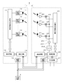
上記の多光軸光電センサSは、単独で動かしてもよいが、図1に示したコード線101や連結用のコードなどを介して複数の光電センサSを連結して動かすこともできる。図3は、この連結例を示すもので、投光器1Aと受光器2Aとの組み合わせによるセンサSAと、投光器1Bと受光器2Bとの組み合わせによるセンサSBと、投光器1Cと受光器2Cとの組み合わせによるセンサSCとの間で、投光器同士および受光器同士が連結されている。また、各連結体の一端に位置する投光器1Aと受光器2Aもケーブルを介して連結されている。
なお、図3では、投光器1A,1B,1Cに関しては制御回路15および通信回路16を、受光器2A,2B,2Cに関しては制御回路25、通信回路26、出力回路27を、それぞれ図2に示した符号により示す。また、以下の説明において、センサSA,SB,SC、投光器1A,1B,1C、および受光器2A,2B,2Cを総称する場合には「センサS」「投光器1」「受光器2」という。さらに、これらの投光器1および受光器2を「機器」と総称する場合もある。
実際のセンサSA,SB,SCの配置では、投光器1および受光器2は、長さ方向に沿って並べられる(縦並び)場合もあれば、幅方向に沿って並べられる(横並び)場合もある。また、各機器を整列させずに配置する場合もある。
図3に示すように、各機器を連結することによって、各投光器1間の制御回路15、および各受光器2間の制御回路25が、それぞれ信号線(マスタ/スレーブ線)を介して直列に接続された状態になる。後述するように、各機器はこの接続を介した信号のやりとりによって、自装置がマスタ機器、スレーブ機器のいずれであるかを認識する。
また各機器の通信回路16,26は、センサSAの投光器1Aおよび受光器2Aを介してループ状に連なる通信回線に接続される。これにより各機器の通信回路16,26は一連に接続された状態となり、個々のセンサSの投光器1と受光器2との間での通信が可能になると共に、異なるセンサSに属する機器の間での通信も可能になる。
各受光器2の出力回路27の各端子は直列に接続され、受光器2Aの受光回路27からの出力が検出信号として外部に出力される。また,図3には示していないが、各機器の電源回路18,28も、外部電源5からの共通ラインに接続された状態になる。
各受光器2の制御回路25は、検出信号の状態のフィードバックを受けるために、出力線に接続される。
この実施例では、投光器1Aと受光器2Aとが直接連結された状態にあるセンサSAが第1位となり、このセンサSAに連結されるセンサSBが第2位となり、センサSBに連結されるセンサSCは第3位となる。またこの実施例では、センサSAの受光器2Aがマスタ機器として機能し、他のセンサSB,SCの投光器1B,1Cおよび受光器2B,2C、ならびにセンサSAの投光器1Aはスレーブ機器に設定される。ただし、センサSAの投光器1Aには、マスタ機器と対をなすスレーブ機器として他の投光器1B,1Cを管理する機能が設定される。
マスタ機器およびスレーブ機器の割り当てや機器間の順位付けは、毎時の起動時に以下のような処理が行われることにより確定する。
まず共通電源からの電源投入により各機器の制御回路15,25が起動すると、各制御回路15,25は、自装置の上方のマスタ/スレーブ線にパルス信号を出力する処理を一斉に開始する。各制御回路15,25は、この出力を続けながら、自装置の下方のマスタ/スレーブ線からパルス信号が入力されるか否かをチェックする。図3の構成によれば、センサSAの投光器1Aおよび受光器2Aにはパルス信号は入力されず、その他の機器はパルス信号の入力を受けることになる。
受光器2Aの制御回路25は、パルス信号の入力がなかったことをもって自装置がマスタ機器であると認識する。そしてパルス信号の出力を停止して、スレーブ機器にアドレスを割り当てるための通信を開始する。以下、適宜、受光器2Aをマスタ機器2Aと言い換える。
他の受光器2B,2Cの制御回路25は、パルス信号が入力されたことをもって自装置がスレーブ機器であると認識する。この後、パルス信号の入力が停止すると、マスタ機器2Aからのコマンドに応答して通信を行い、マスタ機器2Aに自装置の属性(機器の種別や光軸数など)を報知すると共に、アドレスの通知を受けて、これをメモリに登録する。またこれらの処理を実施した受光器2B,2Cでは、上方のマスタ/スレーブ線へのパルス信号の出力を停止する。
したがって、まずマスタ機器2Aからのパルス信号の入力を受けなくなった受光器2Bが先にマスタ機器2Aと通信し、次に受光器2Cが通信を行うことになる。マスタ機器2Aでは、各受光器2B,2Cに通信が可能になった順に順位を設定してアドレスを割り当て、そのアドレスと受光器2B,2Cから報知された属性とを対応づけて登録する。
投光器1Aの制御回路15は、パルス信号が入力されなかったことをもって、自装置をマスタ機器と対をなすスレーブ機器であると認識する。この後は、受光器2B,2Cと同様に、マスタ機器2Aからのコマンドに応答してアドレスの通知を受け、また自装置がマスタ機器2Aに対応する投光器であることを報知する。通信が完了すると、投光器1Aはパルス信号の出力を停止し、以後、受光器2Aの命令に従って、下位の投光器1B,1Cに対し、受光器2Aが受光器2B,2Cに対して実施するのと同様の通信を行う。
投光器1B,1Cは、パルス信号が入力されたことに応じて自装置を一般のスレーブ機器であると認識し、受光器2B,2Cと同様の手順で順に投光器1Aと通信をし、アドレスの通知を受ける。また投光器2B,2Cからも自装置の属性を示す情報が送信される。これらは投光器1Aを介してマスタ機器2Aに送信される。
上記のとおり、この実施例では、センサSAの受光器2Aをマスタ機器として機能させ、投光器1Aにマスタ機器2Aの指示を受けて下位の投光器1B,1Cを管理する機能を付与するが、この関係は逆であってもよい。
上記の接続および各機器間での通信や認識処理によって、センサSA,SB,SCによる物体検知システムが構築される。このシステムでは、最上位のセンサSAを先頭に、SB,SCの順に、他のセンサSの検出処理の期間に重ならないタイミングで検出処理を実行する。いずれかのセンサSの検出処理で光軸の遮光状態が検出されると、そのセンサSの出力回路27からの出力はオフ状態となる。これによりマスタ機器2Aから出力される検出信号もオフ状態となる。
上記のシステムでは、各機器は、従来と同様に検出処理のほか機能処理や自己診断処理を実行するが、各機器でそれぞれ各種処理を実施する期間を独立して管理することによりセンサ間の通信の頻度を最小限に抑えることによって、各種処理を円滑に進行させるようにしている。
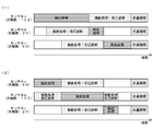
具体的にこの実施例では、各機器の間で図4に示すようなスケジュール情報を共有し、このスケジュール情報に基づき各処理を進行させる。このスケジュール情報では、各機器の検出処理の期間と検出処理以外の処理(機能処理および自己診断)を実施する期間との配分が定められる。
図4では、スケジュール情報について2通りの具体例(1)(2)を示している。各例が適用されるシステムでは、いずれも102本の光軸を有するセンサと、24本の光軸を有するセンサと、60本の光軸を有するセンサとが使用されているが、各例ではセンサの上下関係が異なるため、異なる内容のスケジュール情報が設定されている。
いずれの例でも、左から右に向かう方向に時間軸を設定して、各センサSの処理の進行スケジュールを縦並びにして対比する。各スケジュールには、検出処理の期間のほか、機能処理および自己診断の期間が含まれている。またスケジュール中の白抜き部分は,処理が行われない待ち期間である。
機能処理および自己診断の期間は、他のセンサSとの通信をせずに1つのセンサSで単独で実施する処理(以下、「単独での機能処理および自己診断」という。)の期間と、センサ間での通信が必要な処理(ミューティングの制御やOSSD診断など。以下、これらを「共通処理」という。)の期間とに分けられる。なお、図4では、単独での機能処理および自己診断を「機能処理・自己診断」と記載する。これらの処理ではセンサ間での通信は実施されないが、センサSを構成するペアの投光器1と受光器2との間では、適宜、通信を実行する。
図4に示すように、各センサSのスケジュールは、それぞれの検出処理の期間に重複が生じないようにする一方で、これらの期間がほぼ連続して進行するように設定される。また各センサSの単独での機能処理および自己診断処理がそれぞれ他のセンサの検出処理に並列して実施されるようにしている。また各センサSでの検出処理が一巡したときに全てのセンサSにおいて一斉に共通処理が開始されるようにしている。
各センサSの検出処理期間の長さは、光軸の数が多くなるほど長くなる。これに対し、単独での機能処理および自己診断の内容はいずれのセンサSとも同じであるので、処理に要する時間をほぼ一定にすることができる。そこでこの実施例では、各センサSの検出処理の順番や検出処理期間の長さに基づき、センサ毎に、検出処理の前後の時間の長さに基づき、単独での機能処理および自己診断を実施する期間を割り付けてスケジュールを設定する。
図4(1)(2)の例では、いずれも最初に検出処理を実施する最上位のセンサSAでは検出処理を実施してから機能処理および自己診断を実施するが、後続のセンサSB,SCにおける処理の流れは事例毎に異なる。
具体的に各例を参照すると、図4(1)の例では、センサSAの検出処理期間が単独での機能処理および自己診断に要する時間より長いため、センサSB,SCでは、検出処理より前に単独での機能処理および自己診断が実施されるように設定されている。
一方、図4(2)の例では、センサSAの検出処理期間は単独での機能処理および自己診断に要する時間より短いため、2番目に検出処理を実施するセンサSBでは、検出処理の前と後とに分けて、単独での機能処理および自己診断の期間が設定される。3番目に検出処理を実施するセンサSCでは、検出処理の前に十分な長さの待ち時間が生じるので、単独での機能処理および自己診断の期間は検出処理の前に設定される。
図4(1)(2)には示していないが、機能処理および自己診断には複数種の処理が含まれ、実際のスケジュール情報ではこれらの処理毎に実施時期が定められる。各処理の進行順序は一定であってもよいが、図4(2)のセンサSBの例のように、検出処理の前後に期間を分けて機能処理および自己診断を実施する場合には、各期間の長さと各種処理に要する時間長さとの関係に基づいて、処理の順序を変更してもよい。
共通処理の期間に関しても同様に、複数種の処理に関する進行順序や実施期間が定められるが、その定義は全てのセンサSで統一されたものとなる。
上記のスケジュール情報は、システムの起動時にマスタ機器2Aにより作成され、マスタ機器2Aから各スレーブ機器に配信される。
また、マスタ機器2Aは、スケジュール情報に示される処理を開始する前に、各スレーブ機器に処理の開始を求めるコマンド信号を一括送信する。各スレーブ機器ではこのコマンド信号の受信から一定時間後に自装置のタイマの動作クロックを立ち上げ直す補正を行うと共に、計時時間をリセットする。またマスタ機器2Aでも、コマンド信号の送信後のクロック数に基づき、各機器とタイミングを合わせて自装置のタイマの計時時間をリセットする。なお、各スレーブ機器でのコマンドの受信から補正までに要する時間は、起動時にマスタ機器2Aとスレーブ機器とが通信をした際に、両者間の通信に要した時間の長さに基づいて装置間での補正タイミングが同期するように設定され、各スレーブ機器のメモリに登録される。
上記の処理により各機器における計時のタイミングが同期し、各タイマの計時時間も整合した状態になるので、対をなす投光器1と受光器2との間で通信をしなくとも、各機器における光軸の選択のタイミングを合わせることができる。また、各センサSの検出処理のタイミングがずれて他のセンサSの検出処理と重なったり、検出処理の順序が狂うような不備が起こるのを防止することができる。センサ間の通信が必要となる共通処理でも、各センサSでの処理の開始タイミングが統一されるので、通信エラーを防ぐことができ、期間内に効率良く処理を行うことができる。
なお、この実施例では、マスタ機器2Aは、スケジュール情報に定められた全ての処理を1サイクル実施するのに必要な時間を認識しつつ、1サイクル分の時間が経過する都度、上記のコマンド信号を送信する。ただし、各機器の動作クロックの精度が確保できるのであれば、マスタ機器2Aは、スケジュール情報に定められた処理が2以上の所定サイクル進行するのに相当する時間をおいて、コマンド信号を送信するようにしてもよい。
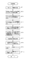
図5は、システムの起動後に、マスタ機器であることを認識したセンサSAの受光器2Aがスケジュール情報の作成および送信のために実施する設定処理の手順を示す。以下、この図5を参照して、設定処理の詳細を説明する。
まず、マスタ機器2Aは、各スレーブ機器と順に通信をして、そのスレーブ機器の属性(投光器1か受光器2か)、光軸数などを認識し、アドレスを割り当てる(ステップST1)。この処理の詳細は、先に図3を参照して説明したとおりである。
各スレーブ機器に対する認識が完了すると、ステップST2では、それぞれの認識結果に基づき、投光器1と受光器2との対応関係やセンサSの数を認識する。
つぎにステップST3では、各センサSの光軸数に基づいて、センサSA,SB,SC毎に検出処理期間の長さ(以下、「検出処理時間」という。)を算出する。続くステップST4では、タイマをリセットしてからスケジュール情報に示す処理を開始するまでの待ち時間としてあらかじめメモリに登録されている時間長さを読み出し、これを待ち時間に設定する。なお、この待ち時間は、どのセンサの受光器がマスタ機器になっても良いように、全ての受光器2のメモリに登録されている。
さらにステップST5において、マスタ機器2Aは、上記の待ち時間や各センサSの検出処理時間を用いて、センサS毎に、検出処理の開始時期および終了時期を設定する。これらの時期はタイマの計時時間により表される。また、この設定では、それぞれのセンサSの検出処理が完全に連続するような設定をしても良いが、各検出処理の間に若干の余裕時間を設けてもよい。または、それぞれのセンサSの検出処理時間を、光軸数から割り出される長さより少し長めに設定してもよい。
ステップST6では、センサS毎に、そのセンサの検出処理期間の前後の空き時間の長さを導出し、その結果に基づき、単独での機能処理および自己診断処理の実施期間を設定する。このときには、前記したように、複数種の処理毎に具体的な開始時期と終了時期とを定める。これらの時期も、検出処理と同様に、タイマの計時時間により表される。
ステップST7では、センサ間での通信が必要な共通処理の実施期間を設定する。この設定処理でもステップST6と同様に、処理の種毎に開始時期と終了時期とを定める。各時期は、いずれもタイマの計時時間により表される。
この後、マスタ機器2Aは、ステップST8において、上記の各設定の結果を統合することにより、センサS毎に、そのセンサにおける処理の進行スケジュールを示すスケジュール情報を作成する。各スケジュール情報には、インデックス情報として、それぞれ対応するセンサSの投光器1および受光器2のアドレスが付与される。マスタ機器2Aは、ステップST9において各スケジュール情報を自装置のメモリに保存し、さらにステップST10において各スケジュール情報をスレーブ機器に向けて一括送信する。これにより設定処理は終了する。
スレーブ機器では、マスタ機器2Aより送信されたスケジュール情報を全て取り込むが、その中から自装置のアドレスを含むインデックス情報が設定されているものを有効にする。マスタ機器2Aでも同様に、自装置のアドレスを含むインデックス情報が設定されているスケジュール情報を有効にする。
この後、マスタ機器2Aから各スレーブ機器に前述のコマンド信号が送信され、これに応じてマスタ機器2Aを含む各機器のタイマが一斉にリセットされる。以後、各機器は、有効なスケジュール情報(自装置に適合するスケジュール情報)に基づき、各種処理の開始時期や終了時期を判別しながら、該当する処理を実行する。
なお、上記の実施例では、複数のセンサSが連結されて使用されることを前提として説明したが、センサSが単独で使用される場合にも同様に、受光器2がマスタ機器となって、自装置および投光器1のスケジュール情報を作成し、このスケジュール情報に基づき各機器がそれぞれ独立して処理の期間を管理する。
上記の実施例によれば、システムの起動時に各機器が自装置がマスタ機器であるか、スレーブ機器であるかを認識した後に、マスタ機器において図5に示した設定処理を実施することにより、各機器のスケジュール情報を作成してこれを各機器に提供するので、システムの構成が変更された場合にも、その変更に容易に対応することができる。ただし、これに限らず、各機器が連結されて初めて電源が投入されたときに作成されて各機器のメモリに保存されたスケジュール情報を電源遮断後も保存し、外部よりマスタ機器2Aにスケジュール情報の更新を指示する信号が入力されたことに応じて新たなスケジュール情報を作成し、各機器のスケジュール情報を新しい情報に書き換えるようにしてもよい。
S(SA,SB,SC) 多光軸光電センサ 、 1 投光器、 2 多光軸光電センサ、 2A マスタ機器、 1A,1B,1C,2B,2C スレーブ機器、 11 発光素子、 21 受光素子、 14,24 光軸順次選択回路、 15,25 制御回路、 16,26 通信回路
Claims (5)
- 複数の多光軸光電センサの投光器および受光器が通信線を介して相互に接続されると共に、センサ間での通信に基づき、センサ毎の検出処理を順番に進行させる物体検知システムであって、
各多光軸光電センサの投光器および受光器は、それぞれ自装置における動作のタイミングを管理するためのタイマを具備すると共に、これらの機器のうちの1台がマスタ機器として機能し、
前記マスタ機器は、システム内のセンサの関係および各センサの光軸数に基づき、各センサの検出処理の期間と検出処理以外の処理を実施する期間との進行スケジュールを表すスケジュール情報を作成するスケジュール設定手段と、システム内の他の機器にそれぞれ前記スケジュール情報を送信するスケジュール送信手段と、他の各機器に前記スケジュール情報に基づく処理の開始を求めるコマンドを送信するコマンド送信手段とを具備し、
前記マスタ機器以外の各機器はマスタ機器からのコマンドを受信したことに応じてそれぞれのタイマをマスタ機器に同期するように補正し、
マスタ機器を含む各機器は、前記スケジュール情報を記憶する記憶手段と、前記タイマの計時時間に基づきスケジュール情報を参照して自装置が検出処理を実施すべき期間および検出処理以外の処理を実施すべき期間を判別し、判別した各期間にそれぞれ該当する処理を実行する処理実行手段とを、さらに具備する、物体検知システム。 - 前記マスタ機器のスケジュール設定手段は、各センサの検出処理の期間が重なることなく順番に進行すると共に、検出処理以外の処理で各センサが単独で実施可能な処理の期間をそれぞれ他のセンサで検出処理が実施されている期間に並列して割り当てたスケジュール情報を作成する、請求項1に記載された物体検知システム。
- 前記マスタ機器のスケジュール設定手段は、各センサの検出処理が一巡した後にセンサ間での通信が必要な処理を実施する期間が全ての機器に統一して設定されたスケジュール情報を作成する請求項1または2に記載された物体検知システム。
- 前記マスタ機器のコマンド送信手段は、自装置のタイマによる計時時間と前記スケジュール情報とに基づき、スケジュール情報に定義された処理の循環周期を認識しつつ、当該周期が所定サイクル進行する期間に相当する時間が経過したことに応じて、他の機器にそれぞれのタイマを再補正することを求めるコマンドを送信する、請求項1に記載された物体検知システム。
- 前記マスタ機器のスケジュール設定手段は、起動後に他の機器と通信を行うことにより、システム内のセンサの関係および各センサの光軸数を認識し、その認識結果に基づき各機器の検出処理のタイミングを定めて前記スケジュール情報を作成し、前記スケジュール送信手段は、スケジュール情報の作成が完了したことに応じて当該スケジュール情報を他の機器に送信する、請求項1に記載された物体検知システム。
Applications Claiming Priority (2)
| Application Number | Priority Date | Filing Date | Title |
|---|---|---|---|
| JP2011040152A JP5353924B2 (ja) | 2011-02-25 | 2011-02-25 | 物体検知システム |
| JP2011-040152 | 2011-02-25 |
Publications (1)
| Publication Number | Publication Date |
|---|---|
| WO2012114537A1 true WO2012114537A1 (ja) | 2012-08-30 |
Family
ID=46720348
Family Applications (1)
| Application Number | Title | Priority Date | Filing Date |
|---|---|---|---|
| PCT/JP2011/056442 Ceased WO2012114537A1 (ja) | 2011-02-25 | 2011-03-17 | 物体検知システム |
Country Status (2)
| Country | Link |
|---|---|
| JP (1) | JP5353924B2 (ja) |
| WO (1) | WO2012114537A1 (ja) |
Citations (4)
| Publication number | Priority date | Publication date | Assignee | Title |
|---|---|---|---|---|
| WO1998010516A1 (en) * | 1996-09-04 | 1998-03-12 | Omron Corporation | General operation control method and its controller |
| JP2002303684A (ja) * | 2001-04-04 | 2002-10-18 | Keyence Corp | 多光軸光電センサ、その表示制御方法及び表示装置並びに多光軸光電センサシステム |
| JP2006279676A (ja) * | 2005-03-30 | 2006-10-12 | Sunx Ltd | 検出ユニット、センサシステム |
| JP2006317238A (ja) * | 2005-05-11 | 2006-11-24 | Keyence Corp | 多光軸光電式安全装置 |
-
2011
- 2011-02-25 JP JP2011040152A patent/JP5353924B2/ja active Active
- 2011-03-17 WO PCT/JP2011/056442 patent/WO2012114537A1/ja not_active Ceased
Patent Citations (4)
| Publication number | Priority date | Publication date | Assignee | Title |
|---|---|---|---|---|
| WO1998010516A1 (en) * | 1996-09-04 | 1998-03-12 | Omron Corporation | General operation control method and its controller |
| JP2002303684A (ja) * | 2001-04-04 | 2002-10-18 | Keyence Corp | 多光軸光電センサ、その表示制御方法及び表示装置並びに多光軸光電センサシステム |
| JP2006279676A (ja) * | 2005-03-30 | 2006-10-12 | Sunx Ltd | 検出ユニット、センサシステム |
| JP2006317238A (ja) * | 2005-05-11 | 2006-11-24 | Keyence Corp | 多光軸光電式安全装置 |
Also Published As
| Publication number | Publication date |
|---|---|
| JP5353924B2 (ja) | 2013-11-27 |
| JP2012177594A (ja) | 2012-09-13 |
Similar Documents
| Publication | Publication Date | Title |
|---|---|---|
| JP5673187B2 (ja) | 物体検知システム | |
| JP5064197B2 (ja) | 光電センサ | |
| US10514294B2 (en) | Optical measurement apparatus having a synchronizing function of synchronizing time between a master device and a slave device, and connectable to an industrial network | |
| JP5353924B2 (ja) | 物体検知システム | |
| GB2564516A (en) | Control system and control method for controlling memory modules | |
| JP6878931B2 (ja) | センサ制御装置、およびセンサシステム | |
| JP2004214899A (ja) | 多光軸光電センサ | |
| JP5747582B2 (ja) | 多光軸光電センサ | |
| CN105094100B (zh) | 一种舞台多模块协同控制系统 | |
| JP5158335B2 (ja) | Plcのスレーブ | |
| US11749103B2 (en) | Signal processing device | |
| JP7081443B2 (ja) | 信号処理装置、および情報書換装置 | |
| US20150253756A1 (en) | Programmable controller | |
| JP4985979B2 (ja) | プログラマブルロジックコントローラ | |
| JP4846325B2 (ja) | 多光軸光電センサ、投光器、及び受光器 | |
| JP6926990B2 (ja) | 多光軸光電センサ | |
| CN208800320U (zh) | 点胶设备 | |
| JP2000268689A (ja) | 光電センサシステム | |
| JP2002305433A (ja) | 光電センサ | |
| JP3851817B2 (ja) | 光電センサシステム及び光電センサ | |
| US20120105378A1 (en) | Input apparatus and method of controlling the same | |
| JP2002131125A (ja) | 光電センサ及びその駆動方法並びに光電センサシステム | |
| JP5724483B2 (ja) | 多光軸光電センサ | |
| KR101801116B1 (ko) | Pcu 시스템 구동 방법 및 장치 | |
| JP2007272827A (ja) | センサシステム及びセンサユニット |
Legal Events
| Date | Code | Title | Description |
|---|---|---|---|
| 121 | Ep: the epo has been informed by wipo that ep was designated in this application |
Ref document number: 11859518 Country of ref document: EP Kind code of ref document: A1 |
|
| NENP | Non-entry into the national phase |
Ref country code: DE |
|
| 122 | Ep: pct application non-entry in european phase |
Ref document number: 11859518 Country of ref document: EP Kind code of ref document: A1 |