WO2012111384A1 - 正特性サーミスタ - Google Patents
正特性サーミスタ Download PDFInfo
- Publication number
- WO2012111384A1 WO2012111384A1 PCT/JP2012/051330 JP2012051330W WO2012111384A1 WO 2012111384 A1 WO2012111384 A1 WO 2012111384A1 JP 2012051330 W JP2012051330 W JP 2012051330W WO 2012111384 A1 WO2012111384 A1 WO 2012111384A1
- Authority
- WO
- WIPO (PCT)
- Prior art keywords
- thick film
- thermistor
- alumina substrate
- alumina
- positive temperature
- Prior art date
Links
- 239000000758 substrate Substances 0.000 claims abstract description 57
- PNEYBMLMFCGWSK-UHFFFAOYSA-N aluminium oxide Inorganic materials [O-2].[O-2].[O-2].[Al+3].[Al+3] PNEYBMLMFCGWSK-UHFFFAOYSA-N 0.000 claims abstract description 54
- 239000000919 ceramic Substances 0.000 claims abstract description 27
- VYPSYNLAJGMNEJ-UHFFFAOYSA-N Silicium dioxide Chemical compound O=[Si]=O VYPSYNLAJGMNEJ-UHFFFAOYSA-N 0.000 claims abstract description 26
- 239000004065 semiconductor Substances 0.000 claims abstract description 25
- ZOXJGFHDIHLPTG-UHFFFAOYSA-N Boron Chemical compound [B] ZOXJGFHDIHLPTG-UHFFFAOYSA-N 0.000 claims abstract description 23
- 229910052796 boron Inorganic materials 0.000 claims abstract description 23
- 239000000377 silicon dioxide Substances 0.000 claims abstract description 13
- JRPBQTZRNDNNOP-UHFFFAOYSA-N barium titanate Chemical compound [Ba+2].[Ba+2].[O-][Ti]([O-])([O-])[O-] JRPBQTZRNDNNOP-UHFFFAOYSA-N 0.000 claims abstract description 10
- 229910002113 barium titanate Inorganic materials 0.000 claims abstract description 10
- 230000001747 exhibiting effect Effects 0.000 abstract description 3
- 239000010408 film Substances 0.000 description 42
- 238000010438 heat treatment Methods 0.000 description 7
- 239000000843 powder Substances 0.000 description 7
- 238000000034 method Methods 0.000 description 6
- 239000000203 mixture Substances 0.000 description 6
- 238000010304 firing Methods 0.000 description 5
- 230000002950 deficient Effects 0.000 description 3
- 239000011521 glass Substances 0.000 description 3
- 238000005245 sintering Methods 0.000 description 3
- 239000010953 base metal Substances 0.000 description 2
- 238000010586 diagram Methods 0.000 description 2
- 239000012212 insulator Substances 0.000 description 2
- 238000004519 manufacturing process Methods 0.000 description 2
- 239000000463 material Substances 0.000 description 2
- 229910052759 nickel Inorganic materials 0.000 description 2
- 238000004544 sputter deposition Methods 0.000 description 2
- 239000002966 varnish Substances 0.000 description 2
- OYPRJOBELJOOCE-UHFFFAOYSA-N Calcium Chemical compound [Ca] OYPRJOBELJOOCE-UHFFFAOYSA-N 0.000 description 1
- 229910004298 SiO 2 Inorganic materials 0.000 description 1
- 229910010413 TiO 2 Inorganic materials 0.000 description 1
- ATJFFYVFTNAWJD-UHFFFAOYSA-N Tin Chemical compound [Sn] ATJFFYVFTNAWJD-UHFFFAOYSA-N 0.000 description 1
- RTAQQCXQSZGOHL-UHFFFAOYSA-N Titanium Chemical compound [Ti] RTAQQCXQSZGOHL-UHFFFAOYSA-N 0.000 description 1
- QCWXUUIWCKQGHC-UHFFFAOYSA-N Zirconium Chemical compound [Zr] QCWXUUIWCKQGHC-UHFFFAOYSA-N 0.000 description 1
- 239000000956 alloy Substances 0.000 description 1
- 229910045601 alloy Inorganic materials 0.000 description 1
- 229910052787 antimony Inorganic materials 0.000 description 1
- WATWJIUSRGPENY-UHFFFAOYSA-N antimony atom Chemical compound [Sb] WATWJIUSRGPENY-UHFFFAOYSA-N 0.000 description 1
- 229910052788 barium Inorganic materials 0.000 description 1
- DSAJWYNOEDNPEQ-UHFFFAOYSA-N barium atom Chemical compound [Ba] DSAJWYNOEDNPEQ-UHFFFAOYSA-N 0.000 description 1
- 239000011230 binding agent Substances 0.000 description 1
- 238000001354 calcination Methods 0.000 description 1
- 229910052791 calcium Inorganic materials 0.000 description 1
- 239000011575 calcium Substances 0.000 description 1
- 230000000052 comparative effect Effects 0.000 description 1
- 229910052802 copper Inorganic materials 0.000 description 1
- 230000000694 effects Effects 0.000 description 1
- 238000002474 experimental method Methods 0.000 description 1
- 238000000227 grinding Methods 0.000 description 1
- 230000020169 heat generation Effects 0.000 description 1
- 238000002156 mixing Methods 0.000 description 1
- 238000000465 moulding Methods 0.000 description 1
- 229910052758 niobium Inorganic materials 0.000 description 1
- 239000010955 niobium Substances 0.000 description 1
- GUCVJGMIXFAOAE-UHFFFAOYSA-N niobium atom Chemical compound [Nb] GUCVJGMIXFAOAE-UHFFFAOYSA-N 0.000 description 1
- 230000001681 protective effect Effects 0.000 description 1
- 229910052761 rare earth metal Inorganic materials 0.000 description 1
- 229910052712 strontium Inorganic materials 0.000 description 1
- CIOAGBVUUVVLOB-UHFFFAOYSA-N strontium atom Chemical compound [Sr] CIOAGBVUUVVLOB-UHFFFAOYSA-N 0.000 description 1
- 239000010409 thin film Substances 0.000 description 1
- 239000010936 titanium Substances 0.000 description 1
- 229910052719 titanium Inorganic materials 0.000 description 1
- WFKWXMTUELFFGS-UHFFFAOYSA-N tungsten Chemical compound [W] WFKWXMTUELFFGS-UHFFFAOYSA-N 0.000 description 1
- 229910052721 tungsten Inorganic materials 0.000 description 1
- 239000010937 tungsten Substances 0.000 description 1
- 238000007740 vapor deposition Methods 0.000 description 1
- XLYOFNOQVPJJNP-UHFFFAOYSA-N water Substances O XLYOFNOQVPJJNP-UHFFFAOYSA-N 0.000 description 1
- 229910052726 zirconium Inorganic materials 0.000 description 1
Images


Classifications
-
- H—ELECTRICITY
- H05—ELECTRIC TECHNIQUES NOT OTHERWISE PROVIDED FOR
- H05B—ELECTRIC HEATING; ELECTRIC LIGHT SOURCES NOT OTHERWISE PROVIDED FOR; CIRCUIT ARRANGEMENTS FOR ELECTRIC LIGHT SOURCES, IN GENERAL
- H05B3/00—Ohmic-resistance heating
- H05B3/10—Heating elements characterised by the composition or nature of the materials or by the arrangement of the conductor
- H05B3/12—Heating elements characterised by the composition or nature of the materials or by the arrangement of the conductor characterised by the composition or nature of the conductive material
- H05B3/14—Heating elements characterised by the composition or nature of the materials or by the arrangement of the conductor characterised by the composition or nature of the conductive material the material being non-metallic
- H05B3/141—Conductive ceramics, e.g. metal oxides, metal carbides, barium titanate, ferrites, zirconia, vitrous compounds
-
- H—ELECTRICITY
- H01—ELECTRIC ELEMENTS
- H01C—RESISTORS
- H01C7/00—Non-adjustable resistors formed as one or more layers or coatings; Non-adjustable resistors made from powdered conducting material or powdered semi-conducting material with or without insulating material
- H01C7/02—Non-adjustable resistors formed as one or more layers or coatings; Non-adjustable resistors made from powdered conducting material or powdered semi-conducting material with or without insulating material having positive temperature coefficient
-
- H—ELECTRICITY
- H01—ELECTRIC ELEMENTS
- H01G—CAPACITORS; CAPACITORS, RECTIFIERS, DETECTORS, SWITCHING DEVICES, LIGHT-SENSITIVE OR TEMPERATURE-SENSITIVE DEVICES OF THE ELECTROLYTIC TYPE
- H01G11/00—Hybrid capacitors, i.e. capacitors having different positive and negative electrodes; Electric double-layer [EDL] capacitors; Processes for the manufacture thereof or of parts thereof
- H01G11/22—Electrodes
-
- H—ELECTRICITY
- H05—ELECTRIC TECHNIQUES NOT OTHERWISE PROVIDED FOR
- H05B—ELECTRIC HEATING; ELECTRIC LIGHT SOURCES NOT OTHERWISE PROVIDED FOR; CIRCUIT ARRANGEMENTS FOR ELECTRIC LIGHT SOURCES, IN GENERAL
- H05B2203/00—Aspects relating to Ohmic resistive heating covered by group H05B3/00
- H05B2203/02—Heaters using heating elements having a positive temperature coefficient
Definitions
- the present invention relates to a positive temperature coefficient thermistor, and more particularly to a positive temperature coefficient thermistor suitable for use as a heating element through which a large current flows.
- a thermistor composed of a semiconductor ceramic having a positive resistance temperature characteristic (PTC characteristic), that is, a positive temperature coefficient thermistor is widely used as a heating element, for example.
- a heating element using a positive temperature coefficient thermistor is advantageous in that it has a self-control function and thus does not require an external control circuit.
- a positive temperature coefficient thermistor used as a heating element is usually provided with an element body made of a single-plate-shaped semiconductor ceramic obtained by pressure-molding and firing a barium titanate-based semiconductor powder.
- the semiconductor ceramic exhibiting the thermistor characteristics is preferably in the form of a film.
- Patent Document 1 Japanese Patent Application Laid-Open No. 55-130101
- Patent Document 1 Ni, Al and / or RuO 2 powder and glass frit are added to barium titanate semiconductor ceramic powder, and a paste-like mixture using an organic binder is applied onto an insulating substrate.
- a method for manufacturing a thick film type positive characteristic semiconductor element is described, which includes a step of forming a thick film and then baking at 600 to 1000 ° C.
- Patent Document 1 describes that according to the above manufacturing method, a semiconductor thick film having a practically sufficient sheet resistance, in other words, a relatively low resistance can be formed.
- the thick film type positive characteristic semiconductor element described in Patent Document 1 is actually used as a practical element such as a heating element, it can withstand its use between the semiconductor thick film and the insulating substrate. Sufficient adhesion is required, but Patent Document 1 does not have a specific description.
- an object of the present invention is to provide a positive characteristic that has a form in which a thick film serving as a heat source is formed on an insulating ceramic substrate, and has excellent adhesion between the insulating ceramic substrate and the thick film. Is to provide a thermistor.
- an alumina substrate is used as the insulator ceramic substrate.
- a positive temperature coefficient thermistor according to the present invention includes an alumina substrate containing silica, a thermistor thick film having a positive resistance temperature characteristic formed on the alumina substrate, and at least a part of the thermistor thick film in contact with the thermistor thick film. And at least one pair of electrodes opposed to each other.
- the present invention is characterized in that the thermistor thick film is formed of a sintered body of a semiconductor ceramic containing a barium titanate system as a main component and at least a boron element as a subcomponent.
- compositional relationship between the thermistor thick film made of the sintered body of barium titanate-based semiconductor ceramic containing boron element and the above-described alumina substrate is further selected as follows. It is a feature.
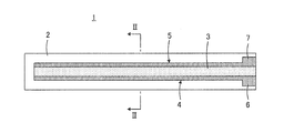
- FIG. 2 is an enlarged sectional view taken along line II-II in FIG. It is a top view which shows the positive temperature coefficient thermistor 11 as a sample produced in the experiment example.
- a positive temperature coefficient thermistor 1 according to an embodiment of the present invention will be described with reference to FIGS.
- the positive temperature coefficient thermistor 1 is in contact with the alumina substrate 2, the thermistor thick film 3 formed on the alumina substrate 2 and exhibiting the PTC characteristic, and the thermistor thick film 3 with at least a part of the thermistor thick film 3 interposed therebetween. And at least one pair of electrodes 4 and 5. Further, although not shown, a protective film may be formed on the alumina substrate 2 so as to cover the thermistor thick film 3 and the electrodes 4 and 5.
- the alumina substrate 2 is made of alumina containing silica. Silica may be used as a sintering aid for alumina substrates.
- the thermistor thick film 3 is ABO 3 (A always contains barium and may further contain at least one selected from strontium, calcium, lead and rare earth elements. B necessarily contains titanium, and further contains tin, zirconium. Sintering of a semiconductor ceramic containing a barium titanate (BaTiO 3 ) system as a main component represented by (ii), niobium, tungsten and antimony) and at least a boron element as a subcomponent Consists of the body. Boron element acts to enable low temperature firing.
- ABO 3 A always contains barium and may further contain at least one selected from strontium, calcium, lead and rare earth elements. B necessarily contains titanium, and further contains tin, zirconium. Sintering of a semiconductor ceramic containing a barium titanate (BaTiO 3 ) system as a main component represented by (ii), niobium, tungsten and antimony) and at least a boron element as a subcomponent Consists
- ⁇ ⁇ ⁇ is less than 0.0015, high adhesion between the alumina substrate 2 and the thermistor thick film 3 cannot be sufficiently ensured.
- ⁇ corresponding to the amount of boron and the equivalent of the amount of silica. This is considered to be because the product of ⁇ to be more than a certain value is required.
- ⁇ corresponding to the amount of boron atom per mole of the BaTiO 3 main component is less than 0.05, sintering of the BaTiO 3 main component does not proceed, resulting in high resistivity, while ⁇ is 1.5 If it exceeds 1, the electrical resistivity of the boron-based glass component is excessively generated and the resistivity is increased.
- the alumina substrate 2 is greatly deformed in the firing step described later for obtaining the sintered thermistor thick film 3 because of insufficient heat resistance of the alumina itself. It comes to occur.
- the boron element contained in the semiconductor ceramic of the present invention exists in the form of an oxide represented by B 2 BaO 4 or B 2 O 3 dissolved in the main component represented by BaTiO 3 ceramic. It may be a thing, and if it contains a boron element, it will not be limited to the said form.
- the thermistor thick film 3 has a thickness of 1 ⁇ m or more, for example.
- a semiconductor ceramic paste formed by mixing semiconductor ceramic powder with varnish is prepared, and this semiconductor ceramic paste is applied onto the alumina substrate 2 or a doctor blade on the alumina substrate 2. After the method or the like is applied to form a sheet, the firing process may be performed.
- the electrodes 4 and 5 have a portion located on the thermistor thick film 3 as well shown in FIG. As shown well in FIG. 1, the first electrode 4 is formed along the longitudinal direction of the thermistor thick film 3 having a rectangular planar shape. On the other hand, the second electrode 5 is positioned so as to face the first electrode 4 with a predetermined distance from the first electrode 4. Further, the electrodes 4 and 5 respectively form wide lead portions 6 and 7 at respective end portions, and these lead portions 6 and 7 are located on one end side of the insulating ceramic substrate 2. .
- the electrodes 4 and 5 are made of a material capable of making ohmic contact with the thermistor thick film 3.
- a material of the electrodes 4 and 5 for example, a base metal such as Ni, Cu, or Al or an alloy thereof, or ohmic Ag that is ohmicized by addition of a base metal is used.
- a thin film forming method such as sputtering or vapor deposition, or a thick film method in which a conductive paste is applied and baked can be applied.
- the positive temperature coefficient thermistor 1 has a structure in which a thermistor thick film 3 is formed in a long pattern on an elongated alumina substrate 2 (that is, an aspect ratio is large). is doing. Therefore, there is a problem that peeling is likely to occur between the alumina substrate 2 and the thermistor thick film 3 due to differences in the respective linear expansion coefficients.
- high adhesion can be ensured between the alumina substrate 2 and the thermistor thick film 3, and therefore, peeling can be prevented. Accordingly, the present invention becomes more significant particularly when the positive temperature coefficient thermistor has a form in which a long thermistor thick film is formed on a long insulator ceramic substrate as shown in FIG.
- varnish is added to the above mixture to form a paste, which is then applied onto an alumina substrate and baked at a temperature of 1050 ° C. for 2 hours to form a thermistor thick film made of a sintered ceramic ceramic having the following composition: Obtained.
- a pair of electrodes 14 is formed on the alumina substrate 12 so as to cover each end of the thermistor thick film 13 formed on the alumina substrate 12. And a positive temperature coefficient thermistor 11 as a sample was obtained.
- room temperature resistivity was measured for each of the obtained samples.
- Room temperature resistivity is measured by the two-terminal method when a DC voltage of 1 V is applied at a room temperature of 25 ° C.
- room temperature resistivity when it was 10 k ⁇ ⁇ cm or more, it was determined to be defective.
- the “amount of deformation of the alumina substrate” was measured for each of the obtained samples.
- the alumina substrate in each obtained sample had a plane size of 3 cm square and a thickness of 0.5 mm, but the “amount of deformation of the alumina substrate” was obtained by placing the sample on a platen having a flat surface. Lay flat with the convex direction of the curve facing up, measure the maximum distance between the upper surface of the sample and the surface plate, calculate the warpage amount of the alumina substrate from this maximum distance, and calculate the warpage amount as ⁇ alumina substrate deformation amount '' It was. When the “deformation amount of the alumina substrate” was 0.3 mm or more, it was determined to be defective.
- FIG. 4 is a diagram showing the relationship between “the atomic ratio ⁇ of element B with respect to 1 mol of the BaTiO 3 main component” and “the Si / Al atomic ratio ⁇ in the alumina substrate” of the sample prepared in this experimental example.
- the region on the dotted line and the region surrounded by the dotted line has the composition within the scope of the present invention.
- the “room temperature resistivity” can be lowered to less than 10 k ⁇ ⁇ cm.
- the thermistor thick film was not peeled off from the alumina substrate, and the alumina substrate was not greatly deformed. These samples satisfy the conditions of 0.0015 ⁇ ⁇ ⁇ ⁇ ⁇ 0.045, 0.05 ⁇ ⁇ ⁇ 1.5, and ⁇ ⁇ 0.2.
- Samples 3, 8 and 13 with ⁇ exceeding 1.5 also had a high resistivity of 10 k ⁇ ⁇ cm or more due to excessive generation of an electrically insulating boron-based glass component.
- These samples 3, 8, and 13 are distributed to the right from the right side of the dotted frame in FIG.
Landscapes
- Engineering & Computer Science (AREA)
- Microelectronics & Electronic Packaging (AREA)
- Ceramic Engineering (AREA)
- Power Engineering (AREA)
- Physics & Mathematics (AREA)
- Electromagnetism (AREA)
- Chemical & Material Sciences (AREA)
- Thermistors And Varistors (AREA)
- Compositions Of Oxide Ceramics (AREA)
Abstract
アルミナ基板上に発熱源となるサーミスタ厚膜が形成された形態を有する正特性サーミスタの低抵抗化を図り、かつサーミスタ厚膜の密着性を高める。 アルミナ基板(2)と、アルミナ基板(2)上に形成された、PTC特性を示すサーミスタ厚膜(3)と、サーミスタ厚膜(3)の少なくとも一部を挟んで対向する1対の電極(4,5)とを備える、正特性サーミスタ(1)において、サーミスタ厚膜(3)は、チタン酸バリウム系を主成分とし、かつ副成分として少なくともホウ素元素を含む、半導体セラミックの焼結体からなり、半導体セラミックにおける、チタン酸バリウム系主成分の1モルに対する、ホウ素元素の含有原子比をαとし、アルミナ基板(2)における、アルミナに対するシリカの含有比率としてのSi/Al原子比をβとしたとき、0.0015≦α×β≦0.045、0.05≦α≦1.5、およびβ≦0.2の条件を満たすようにする。
Description
この発明は、正特性サーミスタに関するもので、特に、大電流が流れる発熱体としての用途に適した正特性サーミスタに関するものである。
正の抵抗温度特性(PTC特性)を有する半導体セラミックをもって構成されたサーミスタ、すなわち正特性サーミスタは、たとえば発熱体として広く利用されている。正特性サーミスタを利用した発熱体は、自己制御機能を有し、よって外部の制御回路を必要としない点で有利である。
発熱体として用いられる正特性サーミスタは、通常、チタン酸バリウム系半導体粉末を加圧成形した後、焼成することによって得られた、単板形状の半導体セラミックからなる素子本体を備えている。しかし、正特性サーミスタが大面積の発熱体として用いられる場合には、サーミスタ特性を示す半導体セラミックは膜状の形態とされることが好ましい。
このような膜状の発熱源を有する半導体素子としては、たとえば、特開昭55-130101号公報(特許文献1)に記載されたものがある。
特許文献1には、チタン酸バリウム系半導体セラミック粉末に、Ni、Alおよび/またはRuO2粉末とガラスフリットとを加え、有機結合剤を用いてペースト状にした混合物を絶縁性基板上に塗布して厚膜状に成形した後、600~1000℃で焼成する、といった工程を備える、厚膜型正特性半導体素子の製造方法が記載されている。
特許文献1には、上記の製造方法によれば、実用上充分な面積抵抗を有する、言い換えると、比較的低抵抗の半導体厚膜が形成できると記載されている。しかし、特許文献1に記載の厚膜型正特性半導体素子が発熱体などの実用的な素子として実際に利用される場合、半導体厚膜と絶縁性基板との間で、その用途に耐え得るに十分な密着性が必要であるが、特許文献1にはそれに関する具体的な記載はない。
そこで、この発明の目的は、絶縁体セラミック基板上に発熱源となる厚膜が形成された形態を有しながら、絶縁体セラミック基板と厚膜との間での密着性に優れた、正特性サーミスタを提供しようとすることである。
この発明では、絶縁体セラミック基板として、アルミナ基板が用いられる。この発明に係る正特性サーミスタは、シリカを含むアルミナ基板と、アルミナ基板上に形成された、正の抵抗温度特性を示すサーミスタ厚膜と、サーミスタ厚膜に接し、かつサーミスタ厚膜の少なくとも一部を挟んで対向する、少なくとも1対の電極とを備える。
また、この発明では、サーミスタ厚膜が、チタン酸バリウム系を主成分とし、かつ副成分として少なくともホウ素元素を含む、半導体セラミックの焼結体からなることを特徴としている。
そして、この発明では、ホウ素元素を含むチタン酸バリウム系の半導体セラミックの焼結体からなるサーミスタ厚膜と前述したアルミナ基板との間での組成的な関係が以下のように選ばれることをさらなる特徴としている。
すなわち、半導体セラミックにおける、チタン酸バリウム系主成分の1モルに対する、ホウ素元素の含有原子比をαとし、アルミナ基板における、アルミナに対するシリカの含有比率としてのSi/Al原子比をβとしたとき、
0.0015≦α×β≦0.045、
0.05≦α≦1.5、および
β≦0.2
の条件を満たすことをさらなる特徴としている。
0.0015≦α×β≦0.045、
0.05≦α≦1.5、および
β≦0.2
の条件を満たすことをさらなる特徴としている。
この発明によれば、後述する実験例によって明らかにされるように、アルミナ基板とサーミスタ厚膜との間で高い密着性を得ることができ、よって剥離等の問題を招きにくくすることができる。したがって、発熱体などの実用的な用途に十分に耐え得る正特性サーミスタを得ることができる。
図1および図2を参照して、この発明の一実施形態による正特性サーミスタ1について説明する。
正特性サーミスタ1は、アルミナ基板2と、アルミナ基板2上に形成された、PTC特性を示すサーミスタ厚膜3と、サーミスタ厚膜3に接し、かつサーミスタ厚膜3の少なくとも一部を挟んで対向する、少なくとも1対の電極4および5とを備えている。さらに、図示しないが、アルミナ基板2上には、サーミスタ厚膜3ならびに電極4および5を覆うように、保護膜が形成されてもよい。
アルミナ基板2は、シリカを含有するアルミナから構成される。シリカはアルミナ基板の焼結助剤として使用されることがある。
サーミスタ厚膜3は、ABO3(Aは、バリウムを必ず含み、さらにストロンチウム、カルシウム、鉛および希土類元素から選ばれる少なくとも1種を含むことがある。Bは、チタンを必ず含み、さらに錫、ジルコニウム、ニオブ、タングステンおよびアンチモンから選ばれる少なくとも1種を含むことがある。)で表わされるチタン酸バリウム(BaTiO3)系を主成分とし、かつ副成分として少なくともホウ素元素を含む、半導体セラミックの焼結体からなる。ホウ素元素は、低温焼成を可能とするように作用する。
そして、半導体セラミックにおける、BaTiO3系主成分の1モルに対する、ホウ素元素の含有原子比をαとし、アルミナ基板2における、アルミナに対するシリカの含有比率としてのSi/Al原子比をβとしたとき、
0.0015≦α×β≦0.045、
0.05≦α≦1.5、および
β≦0.2
の条件を満たすようにされる。
0.0015≦α×β≦0.045、
0.05≦α≦1.5、および
β≦0.2
の条件を満たすようにされる。
ここでいうBaTiO3系主成分の1モルに対するホウ素元素含有原子比とは、BaTiO3系の半導体セラミックのうち、ホウ素元素以外の成分を1モル(分子量)としたときのホウ素元素の含有原子量の比率である。たとえば、半導体セラミックがBaTiO3であれば、α=B/BaTiO3で計算される。
これらの条件を満たすことによって、アルミナ基板2とサーミスタ厚膜3との間で高い密着性を得ることができる。これは、アルミナ基板2中のシリカとサーミスタ厚膜3中のホウ素とが反応することによって、高い密着性を実現しているものと推測される。また、サーミスタ厚膜3において低抵抗率を実現することができる。
α×βが0.0015未満であると、アルミナ基板2とサーミスタ厚膜3との間で高い密着性を十分に確保することができない。これは、上述のように、アルミナ基板2中のシリカとサーミスタ厚膜3中のホウ素とが反応することによって、高い密着性を実現しているため、ホウ素量に相当するαとシリカ量の相当するβとの積が一定以上必要となるためであると考えられる。
他方、α×βが0.045を超えると、ホウ素とシリカとの反応が過度に進み、アルミナ基板2自体が大きく変形するようになる。
また、BaTiO3系主成分の1モルに対するホウ素原子量に相当するαが0.05より少ないと、BaTiO3系主成分の焼結が進まないため、高抵抗率となり、他方、αが1.5を超えると、電気絶縁性のホウ素系ガラス成分の過剰生成により、高抵抗率化する。
シリカ量に相当するβについては、0.2を超えて含有すると、アルミナ自体の耐熱不足のため、焼結したサーミスタ厚膜3を得るための後述する焼成工程において、アルミナ基板2の変形が大きく生じるようになる。
この発明の半導体セラミックに含まれるホウ素元素は、BaTiO3系セラミックで表わされる主成分に固溶しているもの、B2BaO4あるいはB2O3で示される酸化物の状態で存在しているものであってもよく、ホウ素元素を含有していれば、上記形態に限定されるものではない。
サーミスタ厚膜3は、たとえば1μm以上の厚みを有している。サーミスタ厚膜3を形成するため、たとえば、半導体セラミック粉末にワニスを混合して形成した半導体セラミックペーストを用意し、この半導体セラミックペーストをアルミナ基板2上に塗布するか、アルミナ基板2上でドクターブレード法等を適用してシート状に成形するかした後、焼成工程を実施するようにすればよい。
電極4および5は、図2によく示されているように、サーミスタ厚膜3上に位置する部分を有している。第1の電極4は、図1によく示されているように、矩形の平面形状を有するサーミスタ厚膜3の長手方向に沿うように形成されている。他方、第2の電極5は、第1の電極4に対して所定の間隔を隔てながら、第1の電極4に対向するように位置している。また、電極4および5は、それぞれ、各々の端部において幅広の引出し部6および7を形成しており、これら引出し部6および7は、絶縁体セラミック基板2の一方端側に位置している。
電極4および5は、サーミスタ厚膜3との間でオーミック接触が取れる材料から構成される。電極4および5の材料としては、たとえば、Ni、Cu、Al等の卑金属またはその合金、あるいは卑金属添加によりオーミック化されたオーミックAg等が用いられる。
電極4および5を形成するにあたっては、たとえば、スパッタリング、蒸着等の薄膜形成法、または導電性ペーストを塗布して焼き付ける厚膜法を適用することができる。
図示した正特性サーミスタ1は、特に図1からわかるように、長尺状の(すなわち、アスペクト比が大きい)アルミナ基板2上にサーミスタ厚膜3が長尺状のパターンをもって形成された構造を有している。そのため、アルミナ基板2とサーミスタ厚膜3との間で、各々の線膨張係数の違い等が原因となって剥がれが生じやすいという課題がある。しかし、この発明によれば、アルミナ基板2とサーミスタ厚膜3との間で高い密着性を確保でき、よって、剥がれが生じにくくすることができる。したがって、この発明は、特に、正特性サーミスタが図1に示すような長尺の絶縁体セラミック基板上に長尺のサーミスタ厚膜が形成された形態を有するとき、より意義深いものとなる。
次に、この発明の効果を確認するために実施した実験例について説明する。
[実験例]
まず、BaCO3、TiO2およびSm2O3の各粉末を用意し、これら粉末を(Ba0.998Sm0.002)TiO3となるように調合し、次いで、ボールミルを用いて、水中でPSZボールとともに5時間粉砕した後、1000℃の温度で2時間仮焼した。得られた仮焼粉に、表1の「α」((Ba0.998Sm0.002)TiO31モルに対する、ホウ素元素の含有原子比(B/(Ba0.998Sm0.002)TiO3))の欄に示す添加量となるように、BNとBaCO3とを添加して、以下の組成のような混合物を得た。
まず、BaCO3、TiO2およびSm2O3の各粉末を用意し、これら粉末を(Ba0.998Sm0.002)TiO3となるように調合し、次いで、ボールミルを用いて、水中でPSZボールとともに5時間粉砕した後、1000℃の温度で2時間仮焼した。得られた仮焼粉に、表1の「α」((Ba0.998Sm0.002)TiO31モルに対する、ホウ素元素の含有原子比(B/(Ba0.998Sm0.002)TiO3))の欄に示す添加量となるように、BNとBaCO3とを添加して、以下の組成のような混合物を得た。
(Ba0.998Sm0.002)TiO3+αBN+(α/2)BaCO3
他方、表1の「β」(Si/Al原子比)となるSiO2量を有するアルミナ基板を用意した。
他方、表1の「β」(Si/Al原子比)となるSiO2量を有するアルミナ基板を用意した。
次に、上記混合物にワニスを添加し、ペースト化した後、アルミナ基板上に塗布して1050℃の温度で2時間焼成して、以下の組成の半導体セラミックの焼結体からなるサーミスタ厚膜を得た。
Ba0.998Sm0.002TiO3+(α/2)B2O3+(α/2)BaO
焼成後のサーミスタ厚膜の厚みtは100μmであった。
焼成後のサーミスタ厚膜の厚みtは100μmであった。
次に、Niスパッタリングを実施することによって、図3に示すように、アルミナ基板12上に形成された上記サーミスタ厚膜13の各端部を覆う状態で、アルミナ基板12上に1対の電極14および15を形成し、試料となる正特性サーミスタ11を得た。
次に、表1に示すように、得られた各試料について、「室温抵抗率」を測定した。「室温抵抗率」は、室温25℃において、1Vの直流電圧を印加した際の抵抗率を2端子法で測定したものである。この「室温抵抗率」に関して、10kΩ・cm以上の場合、不良と判定した。
また、得られた各試料について、「基板からの剥がれ」を評価した。「基板からの剥がれ」は、アルミナ基板からサーミスタ厚膜が少しでも剥がれていることが目視で確認されたら不良と判定し、表1において「×」で示し、剥がれが生じていないことが確認されたら良好と判定し、「○」で示した。
また、得られた各試料について、「アルミナ基板の変形量」を測定した。得られた各試料におけるアルミナ基板は、3cm角の平面寸法および0.5mmの厚みを有するものであったが、「アルミナ基板の変形量」は、平坦面を有する定盤上に、試料を、湾曲の凸方向を上に向けて平置きし、試料の上面と定盤との最大距離を測定し、この最大距離からアルミナ基板の反り量を求め、この反り量を「アルミナ基板の変形量」とした。「アルミナ基板の変形量」が0.3mm以上の場合、不良と判定した。

表1において、試料番号に*を付したものは、この発明の範囲外の比較例である。
図4は、この実験例において作製した試料の「BaTiO3系主成分1モルに対するB元素の含有原子比α」と「アルミナ基板におけるSi/Al原子比β」との関係を示す図である。図4において、点線上および点線で囲まれた領域がこの発明の範囲内の組成であることを示している。
表1に示すように、この発明の範囲内の試料2、5~7、10~12、15~17および20~22によれば、「室温抵抗率」を10kΩ・cm未満と低くすることができるとともに、サーミスタ厚膜がアルミナ基板から剥がれることも、アルミナ基板が大きく変形することもなかった。これらの試料は、0.0015≦α×β≦0.045、0.05≦α≦1.5、およびβ≦0.2の条件を満たしている。
これらに対して、α×βが0.0015未満である試料1、4および9では、剥がれが生じた。これらの試料1、4および9は、図4において、点線の枠の下側の斜辺より下方に分布するものである。
他方、α×βが0.045を超える試料13、18、23および27では、「アルミナ基板の変形量」が0.5mm以上と大きくなった。これらの試料13、18、23および27は、図4において、点線の枠の上側の斜辺より上方に分布するものである。
また、αが0.05より少ない試料9、14、19および24では、BaTiO3系主成分の焼結が進まないため、10kΩ・cm以上の高抵抗率となった。これらの試料9、14、19および24は、図4において、点線の枠の左側の辺より左方に分布するものである。
他方、αが1.5を超える試料3、8および13でも、電気絶縁性のホウ素系ガラス成分の過剰生成により、10kΩ・cm以上の高抵抗率となった。これらの試料3、8および13は、図4において、点線の枠の右側の辺より右方に分布するものである。
βが0.2を超える試料24~27では、「アルミナ基板の変形量」が1.5mm以上と大きくなった。これらの試料24~27は、図4において、点線の枠の横軸と平行な上側の辺より上方に分布するものである。
1,11 正特性サーミスタ
2,12 アルミナ基板
3,13 サーミスタ厚膜
4,5,14,15 電極
2,12 アルミナ基板
3,13 サーミスタ厚膜
4,5,14,15 電極
Claims (1)
- シリカを含むアルミナ基板と、
前記アルミナ基板上に形成された、正の抵抗温度特性を示すサーミスタ厚膜と、
前記サーミスタ厚膜に接し、かつ前記サーミスタ厚膜の少なくとも一部を挟んで対向する、少なくとも1対の電極と
を備え、
前記サーミスタ厚膜は、チタン酸バリウム系を主成分とし、かつ副成分として少なくともホウ素元素を含む、半導体セラミックの焼結体からなり、
前記半導体セラミックにおける、チタン酸バリウム系主成分の1モルに対する、ホウ素元素の含有原子比をαとし、前記アルミナ基板における、アルミナに対するシリカの含有比率としてのSi/Al原子比をβとしたとき、
0.0015≦α×β≦0.045、
0.05≦α≦1.5、および
β≦0.2
の条件を満たす、
正特性サーミスタ。
Applications Claiming Priority (2)
| Application Number | Priority Date | Filing Date | Title |
|---|---|---|---|
| JP2011-031569 | 2011-02-17 | ||
| JP2011031569 | 2011-02-17 |
Publications (1)
| Publication Number | Publication Date |
|---|---|
| WO2012111384A1 true WO2012111384A1 (ja) | 2012-08-23 |
Family
ID=46672323
Family Applications (1)
| Application Number | Title | Priority Date | Filing Date |
|---|---|---|---|
| PCT/JP2012/051330 WO2012111384A1 (ja) | 2011-02-17 | 2012-01-23 | 正特性サーミスタ |
Country Status (1)
| Country | Link |
|---|---|
| WO (1) | WO2012111384A1 (ja) |
Citations (3)
| Publication number | Priority date | Publication date | Assignee | Title |
|---|---|---|---|---|
| JPS55130101A (en) * | 1979-03-30 | 1980-10-08 | Tokyo Shibaura Electric Co | Method of manufacting thick film positive temperature coefficient semiconductor element |
| JPH0794260A (ja) * | 1993-07-30 | 1995-04-07 | Toshiba Lighting & Technol Corp | ヒータおよび定着装置 |
| JPH11144912A (ja) * | 1997-11-08 | 1999-05-28 | Shizuoka Prefecture | 半導体チタン酸バリウム膜の成膜方法およびptc薄膜層からなるヒーターミラーへの応用と製造方法 |
-
2012
- 2012-01-23 WO PCT/JP2012/051330 patent/WO2012111384A1/ja active Application Filing
Patent Citations (3)
| Publication number | Priority date | Publication date | Assignee | Title |
|---|---|---|---|---|
| JPS55130101A (en) * | 1979-03-30 | 1980-10-08 | Tokyo Shibaura Electric Co | Method of manufacting thick film positive temperature coefficient semiconductor element |
| JPH0794260A (ja) * | 1993-07-30 | 1995-04-07 | Toshiba Lighting & Technol Corp | ヒータおよび定着装置 |
| JPH11144912A (ja) * | 1997-11-08 | 1999-05-28 | Shizuoka Prefecture | 半導体チタン酸バリウム膜の成膜方法およびptc薄膜層からなるヒーターミラーへの応用と製造方法 |
Similar Documents
| Publication | Publication Date | Title |
|---|---|---|
| JP5099011B2 (ja) | チタン酸バリウム系半導体磁器組成物とそれを用いたptc素子 | |
| JP3746763B2 (ja) | 耐還元性低温焼成誘電体磁器組成物、これを用いた積層セラミックキャパシター及びその製造方法 | |
| US9530547B2 (en) | Laminated PTC thermistor element | |
| JP2008177611A (ja) | 表面実装型負特性サーミスタ | |
| WO2014199752A1 (ja) | セラミック電子部品およびその製造方法 | |
| CN104871270B (zh) | 层叠陶瓷电子部件及其制造方法 | |
| GB2383897A (en) | A conductive paste, laminated ceramic electronic component and method of manufacuture | |
| JP2019140199A (ja) | 積層セラミックコンデンサおよびその製造方法 | |
| JPH03274607A (ja) | 誘電体組成物 | |
| JP5765611B2 (ja) | Ptc素子および発熱モジュール | |
| JP2021170612A (ja) | サーミスタ焼結体および温度センサ素子 | |
| WO2012111384A1 (ja) | 正特性サーミスタ | |
| WO2012111386A1 (ja) | 正特性サーミスタ | |
| JP3506056B2 (ja) | 正の抵抗温度特性を有する積層型半導体セラミック素子、および正の抵抗温度特性を有する積層型半導体セラミック素子の製造方法 | |
| US10002714B2 (en) | Dielectric film and dielectric element | |
| JP5626204B2 (ja) | 半導体磁器組成物、発熱体及び発熱モジュール | |
| JP2016063079A (ja) | 抵抗素子およびその製造方法 | |
| WO2012111385A1 (ja) | 正特性サーミスタ | |
| JP4710097B2 (ja) | 積層型正特性サーミスタ | |
| CN114823135A (zh) | 电介质组合物及电子部件 | |
| JP5115949B2 (ja) | 導電材料および抵抗体用ペースト | |
| JP3757794B2 (ja) | サーミスタ用半導体磁器及びそれを用いたチップ型サーミスタ | |
| CN112759384A (zh) | 陶瓷组成物、陶瓷烧结体及叠层型陶瓷电子元件 | |
| JP2013182932A (ja) | Ptc素子の電極形成方法、及びptc素子 | |
| JP2001135501A (ja) | チップ型サーミスタ |
Legal Events
| Date | Code | Title | Description |
|---|---|---|---|
| 121 | Ep: the epo has been informed by wipo that ep was designated in this application |
Ref document number: 12747062 Country of ref document: EP Kind code of ref document: A1 |
|
| NENP | Non-entry into the national phase |
Ref country code: DE |
|
| 122 | Ep: pct application non-entry in european phase |
Ref document number: 12747062 Country of ref document: EP Kind code of ref document: A1 |
|
| NENP | Non-entry into the national phase |
Ref country code: JP |