WO2012105247A1 - Soa-plcハイブリッド集積偏波ダイバーシティ回路およびその製造方法 - Google Patents
Soa-plcハイブリッド集積偏波ダイバーシティ回路およびその製造方法 Download PDFInfo
- Publication number
- WO2012105247A1 WO2012105247A1 PCT/JP2012/000662 JP2012000662W WO2012105247A1 WO 2012105247 A1 WO2012105247 A1 WO 2012105247A1 JP 2012000662 W JP2012000662 W JP 2012000662W WO 2012105247 A1 WO2012105247 A1 WO 2012105247A1
- Authority
- WO
- WIPO (PCT)
- Prior art keywords
- soa
- plc
- optical waveguide
- cos
- hybrid integrated
- Prior art date
- Legal status (The legal status is an assumption and is not a legal conclusion. Google has not performed a legal analysis and makes no representation as to the accuracy of the status listed.)
- Ceased
Links
Images






Classifications
-
- G—PHYSICS
- G02—OPTICS
- G02B—OPTICAL ELEMENTS, SYSTEMS OR APPARATUS
- G02B6/00—Light guides; Structural details of arrangements comprising light guides and other optical elements, e.g. couplings
- G02B6/24—Coupling light guides
- G02B6/26—Optical coupling means
- G02B6/27—Optical coupling means with polarisation selective and adjusting means
- G02B6/2753—Optical coupling means with polarisation selective and adjusting means characterised by their function or use, i.e. of the complete device
- G02B6/2766—Manipulating the plane of polarisation from one input polarisation to another output polarisation, e.g. polarisation rotators, linear to circular polarisation converters
-
- G—PHYSICS
- G02—OPTICS
- G02B—OPTICAL ELEMENTS, SYSTEMS OR APPARATUS
- G02B6/00—Light guides; Structural details of arrangements comprising light guides and other optical elements, e.g. couplings
- G02B6/10—Light guides; Structural details of arrangements comprising light guides and other optical elements, e.g. couplings of the optical waveguide type
- G02B6/12—Light guides; Structural details of arrangements comprising light guides and other optical elements, e.g. couplings of the optical waveguide type of the integrated circuit kind
- G02B6/12004—Combinations of two or more optical elements
-
- G—PHYSICS
- G02—OPTICS
- G02B—OPTICAL ELEMENTS, SYSTEMS OR APPARATUS
- G02B6/00—Light guides; Structural details of arrangements comprising light guides and other optical elements, e.g. couplings
- G02B6/10—Light guides; Structural details of arrangements comprising light guides and other optical elements, e.g. couplings of the optical waveguide type
- G02B6/12—Light guides; Structural details of arrangements comprising light guides and other optical elements, e.g. couplings of the optical waveguide type of the integrated circuit kind
- G02B6/122—Basic optical elements, e.g. light-guiding paths
- G02B6/1228—Tapered waveguides, e.g. integrated spot-size transformers
-
- G—PHYSICS
- G02—OPTICS
- G02B—OPTICAL ELEMENTS, SYSTEMS OR APPARATUS
- G02B6/00—Light guides; Structural details of arrangements comprising light guides and other optical elements, e.g. couplings
- G02B6/10—Light guides; Structural details of arrangements comprising light guides and other optical elements, e.g. couplings of the optical waveguide type
- G02B6/12—Light guides; Structural details of arrangements comprising light guides and other optical elements, e.g. couplings of the optical waveguide type of the integrated circuit kind
- G02B6/122—Basic optical elements, e.g. light-guiding paths
- G02B6/125—Bends, branchings or intersections
-
- G—PHYSICS
- G02—OPTICS
- G02B—OPTICAL ELEMENTS, SYSTEMS OR APPARATUS
- G02B6/00—Light guides; Structural details of arrangements comprising light guides and other optical elements, e.g. couplings
- G02B6/10—Light guides; Structural details of arrangements comprising light guides and other optical elements, e.g. couplings of the optical waveguide type
- G02B6/105—Light guides; Structural details of arrangements comprising light guides and other optical elements, e.g. couplings of the optical waveguide type having optical polarisation effects
-
- H—ELECTRICITY
- H01—ELECTRIC ELEMENTS
- H01S—DEVICES USING THE PROCESS OF LIGHT AMPLIFICATION BY STIMULATED EMISSION OF RADIATION [LASER] TO AMPLIFY OR GENERATE LIGHT; DEVICES USING STIMULATED EMISSION OF ELECTROMAGNETIC RADIATION IN WAVE RANGES OTHER THAN OPTICAL
- H01S5/00—Semiconductor lasers
- H01S5/02—Structural details or components not essential to laser action
- H01S5/026—Monolithically integrated components, e.g. waveguides, monitoring photo-detectors, drivers
-
- H—ELECTRICITY
- H01—ELECTRIC ELEMENTS
- H01S—DEVICES USING THE PROCESS OF LIGHT AMPLIFICATION BY STIMULATED EMISSION OF RADIATION [LASER] TO AMPLIFY OR GENERATE LIGHT; DEVICES USING STIMULATED EMISSION OF ELECTROMAGNETIC RADIATION IN WAVE RANGES OTHER THAN OPTICAL
- H01S5/00—Semiconductor lasers
- H01S5/50—Amplifier structures not provided for in groups H01S5/02 - H01S5/30
- H01S5/5027—Concatenated amplifiers, i.e. amplifiers in series or cascaded
Definitions
- the present invention relates to an SOA-PLC hybrid integrated polarization diversity circuit including a polarization beam splitter (PBS) as a planar lightwave circuit (PLC) and a semiconductor optical amplifier (SOA), and a manufacturing method thereof.
- PBS polarization beam splitter
- PLC planar lightwave circuit
- SOA semiconductor optical amplifier
- the polarization dependence in an optical waveguide device is preferably practically preferably 0.1 dB or less.
- Polarization diversity circuits are used to eliminate the problem of polarization dependence in optical devices.
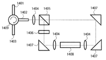
- Non-Patent Document 1 discloses a circulator 1409 having three ports 1401 to 1403, a lens 1404, a half mirror 1405 as a polarization beam splitter, A polarization-independent SOA module for eliminating SOA polarization-dependent gain (PDG) by a polarization diversity circuit using a wave plate 1406, mirror 1407, and SOA 1408 is disclosed.
- PDG SOA polarization-dependent gain
- Non-Patent Document 1 since the polarization-independent SOA module disclosed in Non-Patent Document 1 uses individual optical components that are spatially separated, the size of the entire module increases. In addition, in the module disclosed in Non-Patent Document 1, optical components such as a half mirror 1405 and a mirror 1407 are used. Therefore, in order to form the module shown in FIG. Optical axis adjustment is necessary, which is very time consuming. Therefore, it is difficult to apply the module to other devices. Therefore, it is considered difficult to commercially use the module disclosed in Non-Patent Document 1.
- An object of the present invention is to provide a PLC-SOA hybrid integrated polarization diversity circuit that can reduce the size of a module (circuit) compared to a conventional module and can be easily incorporated into another device.
- the present invention relates to a SOA-PLC hybrid integrated polarization diversity circuit comprising a PLC-PBS chip and a SOA-COS having waveguides coupled to each other, wherein the PLC-PBS chip includes first and second optical waveguides.
- the input light is split into TM mode light and TE mode light, the split TM mode light is output to the first optical waveguide, and the split TE mode light is output to the second light.
- the SOA-COS includes a Mach-Zehnder interferometer circuit that outputs to the optical waveguide of the first and a polarization rotation mechanism formed in the first silica-based optical waveguide through which the TM mode light propagates.
- the SOA-PLC is characterized in that the waveguide and the other end of the fourth optical waveguide not connected to the first optical waveguide and the second optical waveguide are connected to each other by a U-turn optical waveguide.
- a hybrid integrated polarization diversity circuit is provided.
- the PLC-SOA hybrid integrated polarization diversity circuit according to the present invention can reduce the size of the module (circuit) as compared with the conventional module, and can be easily incorporated into other devices.
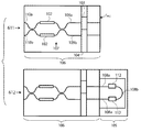
- FIG. 1 is a schematic diagram showing an SOA-PLC hybrid integrated polarization diversity circuit according to a first embodiment of the present invention.
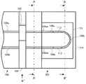
- FIG. 3 is a plan view showing in detail the vicinity of the junction between the PLC-PBS chip and the SOA-COS in the SOA-PLC hybrid integrated polarization diversity circuit according to the first embodiment of the present invention.
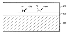
- FIG. 3 is a cross-sectional view of the PLC-PBS chip along the line A-A ′ shown in FIG. 2.
- FIG. 3 is a side view of the vicinity of a recess for forming a half-wave plate of a PLC-PBS chip viewed from the A ′′ direction shown in FIG. 2.
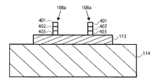
- FIG. 3 is a cross-sectional view of the SOA-COS U-turn semiconductor optical waveguide portion along the line B-B ′ shown in FIG. 2.
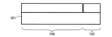
- a schematic diagram showing an example of the arrangement of the PLC-PBS chip and the SOA-COS when the PLC-PBS chip and the SOA-COS are viewed from the side. is there.
- a schematic diagram showing an example of the arrangement of the PLC-PBS chip and the SOA-COS when the PLC-PBS chip and the SOA-COS are viewed from the side. is there.
- FIG. 6 is a plan view showing in detail the vicinity of a junction between a PLC-PBS chip and an SOA-COS in an SOA-PLC hybrid integrated polarization diversity circuit according to a second embodiment of the present invention. It is the figure which expanded the junction part in the facet of the SOA-PLC hybrid integrated polarization diversity circuit concerning 2nd Embodiment of this invention.
- FIG. 1 is a schematic diagram showing a basic configuration of an SOA-PLC hybrid integrated polarization diversity circuit according to the first embodiment of the present invention.
- the SOA-PLC hybrid integrated polarization diversity circuit 100 includes a quartz-based planar lightwave circuit-polarization beam splitter (PLC-PBS) chip 106 and a semiconductor optical amplifier-chip-on-submount (SOA-COS) 105. A configuration in which waveguides are coupled is adopted.
- PLC-PBS quartz-based planar lightwave circuit-polarization beam splitter
- SOA-COS semiconductor optical amplifier-chip-on-submount
- the PLC-PBS chip 106 includes quartz optical waveguides 109 and 110, a slit 104, which is a region where the quartz optical waveguide is partially cut, a Mach-Zehnder interferometer circuit (MZI) 107 as a PBS, and a half-wave plate 103.
- the MZI 107 has an input port 110a and an output port 110b as silica-based optical waveguides, two directional couplers 111, two output ports 109a and 109b as silica-based optical waveguides, and two interferometer arms (heaters) 102. .
- TM mode light is output from the output port 109a of the MZI 107
- TE mode light is output from the output port 109b.
- the half-wave plate 103 is formed in the slit 104 of the output port 109a portion from which TM mode light is output.
- the SOA-COS 105 includes a semiconductor optical waveguide 108 having a straight portion 108a and a U-turn portion 108b, and an SOA chip 113 on which a semiconductor optical amplifier (SOA) 112 formed on the straight portion 108a is formed.
- SOA chip 113 is solder mounted on the silicon bench 114.
- the straight portion 108a of the semiconductor optical waveguide is formed with a buried mesa structure described later, and the U-turn portion 108b of the semiconductor optical waveguide is formed with a high mesa structure described later.
- both the straight portion 108a of the semiconductor optical waveguide and the U-turn portion 108b of the semiconductor optical waveguide can be a high mesa structure or a buried structure.
- the SOA-COS 105 has the U-turn part 108b of the semiconductor optical waveguide, the input / output port 108aa and the input / output port 108ab of the SOA 112 are formed on the PLC-PBS chip 106 side of the SOA-COS 105. That is, by forming the U-turn portion 108b, light can be input and output on the same end face of the SOA-COS 105, and the size of the entire circuit can be reduced.
- the SOA 112 is formed at two locations on the straight portion 108a of the semiconductor optical waveguide. However, if the SOA 112 is long enough to obtain a light amplification effect, the SOA 112 is formed at one location. Also good.
- FIG. 2 is a plan view showing in detail the vicinity of the joint between the PLC-PBS chip 106 and the SOA-COS 105. Specifically, FIG. 2 shows the output port 109a, the output port 109b, the slit 104, and the half-wave plate 103 formed in the slit 104 of the MZI 107 in the PLC-PBS chip 106. FIG. 2 shows the SOA 112, the input / output port 108aa and the input / output port 108ab of the SOA 112, the silicon bench 114, the SOA chip 113, and the straight portion 108a and the U-turn portion 108b of the semiconductor optical waveguide in the SOA-COS 105.
- FIG. 3A is a sectional view of the PLC-PBS chip 106 taken along the line A-A ′ shown in FIG.
- a quartz-based lower cladding layer 303, a core layer 301 constituting the quartz-based optical waveguides 109a and 109b, and an upper cladding layer 302 are formed on the PLC platform 304.
- 3B is a cross-sectional view of the vicinity of the slit 104 of the PLC-PBS chip 106 seen from the direction A ′′ shown in FIG. 2. Propagation loss and reflection return caused by reflection of light propagating through the core layer 301 by the slit 104.
- the slit 104 is not formed perpendicularly to the upper surface of the PLC-PBS chip 106, but is formed at a predetermined angle, as shown in Fig. 3B. Has a width of about 20 to 80 ⁇ m and an inclination of about 5 to 12 ° with respect to the normal of the upper surface.
- FIG. 4 is a cross-sectional view of the U-turn portion 108b of the SOA-COS 105 semiconductor optical waveguide along the line B-B ′ shown in FIG.
- the SOA-COS 105 has a form in which an SOA chip 113 is mounted on a silicon bench 114.
- the SOA chip 113 uses a high mesa structure in which a lower cladding layer 403, a core layer 402 constituting the U-turn portion 108b of the semiconductor optical waveguide, and an upper cladding layer 401 are formed.
- the SOA-COS 105 is formed on a compound semiconductor InP substrate by a microprocess.
- the lower cladding layer 403 is made of InP.
- the core layer 402 is formed of a compound semiconductor InGaAsP.
- the upper cladding layer 401 is made of InP.
- the SOA-COS 105 according to this embodiment or the following embodiments can be formed of a semiconductor material other than InP.
- the waveguide chip according to the present embodiment is not limited to a semiconductor optical waveguide such as SOA.
- the present invention can be applied to all waveguides having polarization dependence, such as LiNbO 3 optical waveguides and silicon-based optical waveguides.
- the relative refractive index difference between the core and the clad constituting the optical waveguide is at most about 2.5%.
- the relative refractive index difference between the core and the clad exceeds 4 to 5%.
- the U-turn type semiconductor optical waveguide (U-turn portion 108b) has a high mesa structure, so that the relative refractive index between the core layer 402 and the dielectric or air on both sides thereof is increased. The difference becomes very large, for example, 30 to 40% or more.
- the radius of curvature of the folded portion when the optical waveguide is folded can be reduced as the relative refractive index difference between the core and the clad increases.
- the radius of curvature is about 125 ⁇ m. Therefore, compared with the case where the folded structure of the U-turn type optical waveguide is formed on the quartz PLC chip, the size of the chip is formed by forming the folded structure of the U-turn type optical waveguide by the high mesa structure on the SOA-COS 105. Can be reduced.
- the U-turn portion 108b is formed as a semiconductor optical waveguide and further has a high mesa structure, whereby the size of the U-turn portion 108b can be reduced, and as a result, the size of the entire circuit can be reduced. it can.
- the SOA 112 is formed by a buried mesa structure in the straight portion 108a of the semiconductor optical waveguide.
- the core layer of the SOA 112 has an active layer (not shown) formed of an optical amplification medium.
- the SOA 112 can also be used as a semiconductor gate for turning on / off incident light by turning on / off an injection current.
- the length of the SOA 112 is, for example, about 0.5 to 2 millimeters.
- the silica-based optical waveguide 109 of the PLC-PBS chip 106 and the linear portion 108a of the semiconductor optical waveguide of the SOA-COS 105 are provided. Aligned and joined.
- the SOA chip 113 of the SOA-COS 105 is thinner than the PLC-PBS chip 106. Therefore, the SOA chip 113 is mounted on the silicon bench 114. By doing so, it becomes possible to increase the area of the joining portion when joining the PLC-PBS chip 106 and the SOA-COS 105, which is sufficient for joining the PLC-PBS chip 106 and the SOA-COS 105. Strength can be obtained.
- the PLC-PBS chip 106 and the SOA-COS 105 perform waveguide coupling for each chip.
- a silicon substrate terrace structure in which the base silicon substrate 501 is shared by the respective chips can be used. Also in this embodiment, the base silicon substrate 501 is shared, but the waveguides of the PLC-PBS chip 106 and the SOA-COS 105 are coupled. This waveguide coupling mode can be applied to all the following embodiments.
- unpolarized light from the input IN is propagated by the circulator 101 to the SOA-PLC hybrid integrated polarization diversity circuit 100.
- the light from the SOA-PLC hybrid integrated polarization diversity circuit 100 is propagated by the circulator 101 to the output OUT.
- a Mach-Zehnder interferometer circuit has a phase difference of ⁇ between two arms.
- the phase difference in the TE mode and TM mode changes independently.
- is expressed by (2 ⁇ / ⁇ ) B ⁇ L
- ⁇ is the wavelength
- B is the birefringence in MZI
- L is the arm length of MZI.
- MZI splits the incident non-polarized light into two orthogonal optical modes (ie, TE mode and TM mode).
- TE mode is output to one output port
- TM mode is output to the other output port.
- the unpolarized light propagated from the circulator 101 is divided into two orthogonal modes (ie, TE mode and TM mode) by the MZI 107.
- the TE mode light emitted from the MZI 107 is propagated to the output port 109b
- the TM mode light is propagated to the output port 109a.
- the TM mode light output from the output port 109 a is changed to TE mode light by the half-wave plate 103.
- only the TE mode light is propagated to the SOA-COS 105.
- a typical semiconductor optical amplifier has, for example, a 5-quantum well structure, and has a saturation power of 12 dB and a low noise figure of approximately 4 dB or less.
- the polarization dependent gain of the semiconductor optical amplifier itself is about 10 to 20 dB.
- the TE mode light has a small signal gain of about 19 dB, but the TM mode light is absorbed and has a gain of about ⁇ 10 to 0 dB. Therefore, by transmitting only the TE mode light to the SOA-COS 105 as in this embodiment, a large gain can be obtained and the polarization dependent gain (PDG) of the SOA 112 can be reduced.
- PDG polarization dependent gain
- the conventional polarization-independent SOA module uses individual optical components that are spatially separated, so that the overall size of the module becomes relatively large, and optical components such as a half mirror are used. Therefore, there is a problem that it is difficult to apply such as mass-producing the module and incorporating it into another device because it takes time and effort to adjust the optical axis between optical components by the user.
- the U-turn part 108b is provided in the SOA-COS 105 so that light can be input and output from one end face of the SOA-COS 105, the polarized waves are separated, and the separated polarized waves are unified.
- the PLC-SOA hybrid integrated polarization diversity circuit is configured to guide both the input light and the output light to the SOA-COS 105 to the configured PLC-PBS chip 106. Therefore, unlike the prior art, it is not necessary to provide an input path and an output path to the SOA separately, and the size of the module (circuit) can be reduced as compared with the conventional polarization-independent SOA module.
- a PLC as a planar lightwave circuit having an MZI 107 as a PBS and a half-wave plate 103 formed in a waveguide on the TM mode output side of the MZI 107 without using optical components such as a half mirror and a lens. -Since the PBS chip 106 is used, the user does not need to bother adjusting the optical axis.
- the waveguides of the SOA-COS 105 and the PLC-PBS chip 106 which are waveguide chips, are combined to form a single waveguide device, it can be incorporated into other devices. Easy to apply. The circuit is therefore very effective for commercial use.
- the polarization dependent gain (PDG) of the SOA 112 can be reduced.
- an optical waveguide is formed of a quartz-based material by combining microfabrication techniques on a substrate such as silicon or quartz.
- a planar lightwave circuit deposits glass particles as a lower cladding layer and a core layer on a PLC substrate (for example, a silicon substrate) by a flame direct deposition (FHD) method, which is an application of optical fiber manufacturing technology. And heated to melt and clear the glass film. Thereafter, a desired optical waveguide pattern is formed by photolithography and reactive ion etching which are semiconductor integrated circuit manufacturing techniques, and an upper cladding is formed again by the FHD method.
- FHD flame direct deposition
- Birefringence can be trimmed by locally heating or irradiating a quartz glass waveguide.
- a polarization beam splitter PBS
- PBS polarization beam splitter
- the heater 102 is formed on the two arms of the MZI 107 in order to trim the birefringence in the MZI 107. During trimming with the heater 102, the phase difference between the two arms of the MZI is measured to be appropriate.
- the PLC-PBS chip 106 is set to have a polarization extinction ratio of a predetermined value (for example, 15 dB) at a predetermined light wavelength (for example, 1530 nm).
- the slit 104 is formed between the two output ports of the MZI 107 and the SOA-COS 105 so as to intersect the silica-based optical waveguide 109 perpendicularly.
- the slit 104 is formed using a dicer or the like, and is formed with an inclination of a predetermined angle with respect to the upper surface of the PLC-PBS chip 106 in order to prevent reflection of light as shown in FIG. 3B. Is done.
- the silica-based optical waveguide 109 of the PLC-PBS chip 106 and the linear portion 108a of the semiconductor optical waveguide of the SOA-COS 105 are in contact with each other on one contact surface. Aligned and joined.
- the SOA-PLC hybrid integrated polarization diversity circuit according to this embodiment is manufactured as in the following manufacturing method.
- a PLC-PBS chip 106 on which quartz-based optical waveguides 110a, 110b, 109a, 109b and a heater 102 are formed is prepared.
- the test light is propagated from the quartz-based optical waveguides 110a and 110b side, heat is applied to the heater 102, and trimming is performed appropriately, and adjustment is performed so that the phase difference between the two arms of the MZI 107 is appropriate.
- the facet f PLC to which the SOA-COS 105 of the PLC-PBS chip 106 is bonded is corrected to a sufficiently small surface roughness by optical polishing.
- a cross section of the PLC-PBS chip 106 coupled to the straight portion 108a and the U-turn portion 108b of the semiconductor optical waveguide is formed.
- the slit 104 is formed by a dicer or the like so as to have a predetermined angle rather than perpendicular to the upper surface of the PLC-PBS chip 106.
- a half-wave plate 103 is formed in the slit 104.
- the half-wave plate 103 is formed on the silica-based optical waveguide side 109 a that transmits TM mode light from the MZI 107.
- the SOA-COS 105 in which the linear portion 108 a and the U-turn portion 108 b of the semiconductor optical waveguide and the SOA 112 are formed is prepared.
- a bonding surface that is coupled to the PLC-PBS chip 106 is formed.
- the quartz optical waveguide and the semiconductor optical waveguide that are in contact with each other are aligned, and the PLC-PBS chip 106 and the SOA-COS 105 are fixed with an adhesive or the like.
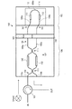
- FIG. 7 is a schematic diagram showing a configuration of an SOA-PLC hybrid integrated polarization diversity circuit 700 according to the second embodiment of the present invention.
- the SOA-PLC hybrid integrated polarization diversity circuit 700 according to the second embodiment is substantially the same as the configuration of the SOA-PLC hybrid integrated polarization diversity circuit 100 according to the first embodiment. Therefore, this embodiment includes the functions and effects of the SOA-PLC hybrid integrated polarization diversity circuit according to the first embodiment.
- a configuration 701 for reducing light propagation loss due to a difference in mode field diameter and reflection on the coupling surface of the waveguide is used.
- FIG. 8A shows details of the configuration 701.
- the configuration 701 includes spot size converters (SSC) 802a and 802b, which are not perpendicular to the joint surface f1 between the PLC-PBS chip 106 and the SOA-COS 105, but at a predetermined angle.
- SSC spot size converters
- FIG. 8B is a partially enlarged view of the joint portion on the joint surface f1. As shown in FIG 8B, so that the light propagates is obliquely incident on the joint surfaces f1, the center axis C1 is a predetermined angle theta 1 inclined with respect to joint surfaces f1.
- the inclined semiconductor optical waveguide ie, SSC 802a and 802b having the central axis C2 of the core is smoothly connected to the straight portion 108a of the semiconductor optical waveguide. It tilted semiconductor optical waveguide and is SSC802a, 802b for joining face f1, by a predetermined angle theta 2 inclined.
- the inclination angles ⁇ 1 and ⁇ 2 are determined so as to satisfy this relationship.
- an antireflection (AR) coat 803 is coated on the joint surface f1 on the SOA-COS 105 side.
- the inclination angle ⁇ 1 on the PLC side is preferably 5 to 9 °
- the inclination angle ⁇ 2 on the semiconductor waveguide side is preferably 12 ° to 17 °.
- the SSCs 802a and 802b are tapered so that the mode field of the silica-based optical waveguides 801a and 801b in the vicinity of the joint surface of the SOA-COS 105 of the PLC-PBS chip 106 matches the mode field of the linear portion 108a of the semiconductor optical waveguide.
- This is an optical waveguide (wide flare type SSC).
- the SSCs 802a and 802b are bent at the site B while maintaining the width at the site A, and the taper is widened at the site C, and the width is widened at the site D and formed in parallel. Is done.
- the SSCs 802a and 802b are formed on the SOA-COS 105 side, but may be formed on the PLC-PBS chip 106 side.
- the SSCs 802a and 802b can reduce the coupling loss at the coupling portion of each waveguide and obtain high coupling efficiency.
- the mode field of each waveguide is different.
- the (electric field distribution) is different from each other.
- the mode field diameter of a silica-based optical waveguide is approximately 3 to 8 ⁇ m
- the mode field diameter of an InP semiconductor optical waveguide is approximately 1 to 2 ⁇ m.
- the silica-based optical waveguide in the PLC-PBS chip 106 and the semiconductor optical waveguide of the SOA-COS 105 are coupled, the light propagation loss due to the difference in mode field diameter and the reflection at the joint surface are reduced.
- the configuration 701 is used.
- the configuration 701 according to the present embodiment can correct a difference in mode field diameter using spot size converters (SSC) 802a and 802b. Further, the reflection can be reduced by coupling the optical waveguides of the respective chips with a predetermined angle. Furthermore, the loss of light propagation caused by reflection is reduced by coating the anti-reflection (AR) coating 803 on the bonding surface f1 on the SOA-COS 105 side (the bonding surface between the PLC-PBS chip 106 and the SOA-COS 105). Can do.
- SSC spot size converters
- the silica-based optical waveguide in the PLC-PBS chip 106 and the semiconductor optical waveguide of the SOA-COS 105 are coupled, the propagation loss of light due to the difference in mode field diameter is reduced. Reflection at the joint surface can be reduced.
- FIG. 8A light is incident on the optical waveguides 801a and 801b inclined from the linear portion 109a of the silica-based optical waveguide.
- the light does not enter perpendicularly to the joint surface f1 as in the first embodiment, but enters at a predetermined angle. Since light is incident on the joint surface f1 at a predetermined angle, it is difficult for light reflected by the joint surface f1 to return to the inclined optical waveguides 801a and 801b. Therefore, the reflected return light at the joint surface f1 to the quartz optical waveguide 109 is reduced.
- the light when light propagates through the SOA-COS 105 and returns to the PLC-PBS chip 106, the light is incident on the tilted semiconductor optical waveguides (ie, SSCs 802a and 802b).
- the light does not enter perpendicularly to the joint surface f1 as in the first embodiment, but enters at a predetermined angle. Since light is incident on the bonding surface f1 at a predetermined angle, it is difficult for the reflected light from the bonding surface f1 to return to the SSCs 802a and 802b again. Therefore, the reflected return light at the joint surface f1 to the SSCs 802a and 802b is reduced.
- the manufacturing method of the SOA-PLC hybrid integrated polarization diversity circuit according to the second embodiment is substantially the same as the manufacturing method of the circuit according to the first embodiment.
- the other portions are substantially the same as the configuration of the circuit according to the first embodiment. Therefore, it is omitted.
- Silica-based optical waveguides 801 a and 801 b that are inclined in the horizontal direction by an angle ⁇ 1 with respect to the direction perpendicular to the facet f PLC serving as a joint surface with the silica-based optical waveguides 110 and 109 and the SOA-COS 105, and the heater 102
- the PLC-PBS chip 106 having the above structure is prepared. Test light is propagated from the silica-based optical waveguide 110 side, and light passing through the heater 102 is measured on the silica-based optical waveguide 109 side. During the measurement, heat is applied to the heater 102 to perform appropriate trimming, and adjustment is performed so that the phase difference between the two arms of the MZI 107 is appropriate.
- an excess portion of the PLC-PBS chip 106 is cut along a broken line A. That is, the silica-based optical waveguide 801a, 801b in any point of the linear portion of the angle theta 1, so as to form a facet f PLC, is cut by a dicer or the like end of the PLC-PBS chip 106.
- the facet f PLC formed by cutting is corrected to a sufficiently small surface roughness by optical polishing.
- a cross section of the PLC-PBS chip 106 coupled to the semiconductor optical waveguides 802a and 802b is formed.
- a slit 104 having a predetermined angle rather than perpendicular to the upper surface of the PLC-PBS chip 106 is formed by a dicer or the like.
- a half-wave plate 103 is formed in the slit 104.
- the half-wave plate 103 is formed on the side of the quartz optical waveguide 109 a that transmits TM mode light from the MZI 107.
- the straight portion 108a of the semiconductor optical waveguide and a predetermined angle of the tapered semiconductor optical waveguide (the angle between the perpendicular of the joint surface f1 and the central axis C2 is ⁇ 2. 2), the SOA-COS 105 having the SSCs 802a and 802b and the SOA 112 inclined to each other is prepared.
- SOA-COS 105 is a semiconductor optical waveguide 802a, the emission angle of 802b is cleaved so that theta 2, facet f SOA of SOA-COS 105 that bind to PLC-PBS chip 106 is formed.
- the straight line portion 108a and the SOA 112 of the semiconductor optical waveguide are formed by a buried mesa structure, the U-turn portion 108b of the semiconductor optical waveguide is formed by a high mesa structure, and the facet f SOA of the SOA-COS 105 is coated with an AR coat 803. Yes.
- the optical waveguides of the respective chips are aligned, and the respective chips are fixed with an adhesive or the like.
- the facet f PLC on the side of the PLC-PBS chip and the facet f SOA on the side of the SOA-COS are opposed to each other at the joint surface f1 of the waveguide, so that the silica-based optical waveguide 801a and the semiconductor waveguide 802a, the silica-based optical waveguide 801b and the semiconductor Waveguides 802b are formed in spaces where they are optically coupled. Note that the processing content and the order of the steps included in the above steps 1 to 4 may be appropriately adjusted.
- FIG. 10 is a schematic diagram showing a configuration of an SOA-PLC hybrid integrated polarization diversity circuit 1000 according to the third embodiment of the present invention.
- the SOA-PLC hybrid integrated polarization diversity circuit 1000 according to the third embodiment is substantially the same as the configuration of the SOA-PLC hybrid integrated polarization diversity circuit according to the first embodiment and the second embodiment.
- the present embodiment includes the functions and effects of the SOA-PLC hybrid integrated polarization diversity circuit according to the first and second embodiments.
- the folded portion of the optical waveguide is not formed in the SOA-COS 1001, but a U-turn-shaped silica-based optical waveguide 1003 is formed in the U-turn PLC chip 1002, and the light amplified by the SOA 112 is MZI107. I'm trying to go back.
- the SOA 112 is formed in a straight portion of the semiconductor optical waveguide of the SOA-COS 1001. That is, in the third embodiment, the light propagated from the PLC-PBS chip 106 is amplified by the SOA 112 formed in the SOA-COS 1001, and is transmitted through the U-turn quartz optical waveguide 1003 formed in the U-turn PLC chip 1002. It is folded back and amplified again by the SOA 112 formed in the SOA-COS 1001, and returns to the PLC-PBS chip 106.
- the waveguide uses the configuration 701 for reducing the light propagation loss due to the difference in the core size and the reflection at the joint surface.
- the radius of curvature of the folded portion can be reduced as the optical waveguide has a larger relative refractive index difference, and as a result, the size of the entire circuit can be reduced.
- a semiconductor waveguide having a buried mesa structure suitable for SOA and a semiconductor waveguide having a high mesa structure suitable for U-turn having a small curvature radius It is not always easy to combine them in the same chip.
- the SOA-PLC hybrid integrated polarization diversity circuit according to this embodiment is slightly larger in overall size, but it is easy to fabricate the SOA-COS. Thus, the feasibility of the polarization diversity circuit is enhanced.
- the manufacturing method of the SOA-PLC hybrid integrated polarization diversity circuit according to the third embodiment is substantially the same as the manufacturing method of the circuit according to the first and second embodiments.
- the manufacturing method of the circuit according to the first and second embodiments is substantially the same as the manufacturing method of the circuit according to the first and second embodiments.
- FIG. 8 only the vicinity of the configuration 701 at the junction of the PLC-PBS chip 106, the SOA-COS 1001, and the U-turn PLC chip 1002 is described in detail. Other parts are omitted because they are substantially the same as the configuration of the circuit according to the first and second embodiments.
- the silica-based optical waveguides 110 and 109, the silica-based optical waveguides 801a and 801b inclined at a predetermined angle, and the PLC-PBS chip 106 on which the heater 102 is formed are prepared. Test light is propagated from the silica-based optical waveguide 110 side, and light passing through the heater 102 is measured on the silica-based optical waveguide 109 side. During the measurement, heat is applied to the heater 102 to perform appropriate trimming, and adjustment is performed so that the phase difference between the two arms of the MZI 107 is appropriate.
- a U-turn PLC chip 1002 is prepared in which a U-turn-shaped silica-based optical waveguide 1003, a silica-based optical waveguide 109, and silica-based optical waveguides 801a and 801b inclined at a predetermined angle are formed.
- the sections of the PLC-PBS chip 106 and the U-turn PLC chip 1002 coupled to the semiconductor optical waveguides 802a and 802b are formed. Further, a slit 104 having a predetermined angle rather than perpendicular to the upper surface of the PLC-PBS chip 106 is formed by a dicer or the like. A half-wave plate 103 is formed in the slit 104. The half-wave plate 103 is formed on the side of the quartz optical waveguide 109 a that transmits TM mode light from the MZI 107.
- an SOA-COS 1001 in which a linear portion 108a of a semiconductor optical waveguide, inclined SSCs 802a and 802b, which are tapered semiconductor optical waveguides, and an SOA 112 are prepared.
- the SOA-COS 1001 is cleaved so that the emission angle of the semiconductor optical waveguides 802a and 802b becomes ⁇ 2 (see FIG. 8B), and the facet f SOA of the SOA-COS 1001 coupled to the PLC-PBS chip 106 and the U-turn PLC chip 1002 Is formed.
- the AR coating 803 is coated on the facet f SOA which is the cut surface of both of the SOA-COS 1001.
- the optical waveguides of the respective chips are aligned, and the respective chips are fixed with an adhesive or the like.
- the facet f PLC on the side of the PLC-PBS chip and the U-turn PLC chip and the facet f SOA on the side of the SOA-COS face each other so that the silica-based optical waveguide 801a, the semiconductor waveguide 802a, The quartz-based optical waveguide 801b and the semiconductor waveguide 802b are formed in spaces where they are optically coupled. Note that the processing content and the order of the steps included in the above steps 1 to 4 may be appropriately adjusted.
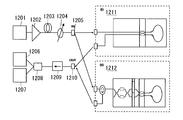
- FIG. 12 shows two PDG measurement configurations for measuring SOA polarization dependent gain (PDG).
- FIG. 12 shows an adjustable light source (TLS) 1201, an erbium-doped optical fiber amplifier (EDFA) 1202, a polarization controller (PC) 1203, an attenuator (ATT) 1204, an input-side optical switch 1205, and an optical spectrum analyzer (OSA).
- TLS adjustable light source
- EDFA erbium-doped optical fiber amplifier
- PC polarization controller
- ATT attenuator
- OSA optical spectrum analyzer
- OPM optical power meter
- the configuration 1211 has a configuration in which an ST-PLC chip having two straight optical waveguides, a SOA-COS having an SOA, and a U-PLC chip having a U-turn optical waveguide are joined.
- the configuration 1211 does not include a circulator and a polarization beam splitter as compared with the configuration 1212.
- the configuration 1211 When light is incident on the configuration 1211 from the TLS 1201, the configuration 1211 does not use a PDC. Therefore, the light propagating through the configuration 1211 propagates in one direction from the input side optical switch 1205 to the output side optical switch 1210 as it is.
- a measurement result in the case of incidence is shown in a graph indicated by reference numeral 1312 in FIG. 13A. Note that the scales of the graphs indicated by reference numerals 1311 to 1314 in FIG.
- 13A are 1549.5 to 1550 to 1550.5 (nm) on the horizontal axis, ⁇ 60 to 0 to +10 (dBm) on the vertical axis, and the upper thick line Is the spectrum of the output light after passing through the configuration 1211 and the configuration 1212, and the lower spectrum is the spectrum of the input light.
- a measurement result when light is incident is shown in a graph indicated by reference numeral 1314 in FIG. 13A.
- the return loss of propagating light was reduced to ⁇ 50 dB or less by setting ⁇ 1 to 15 ° and ⁇ 2 to 7 °.
- an amplification gain of 5.8 dB was obtained in the case of the TE mode light, but a negative amplification gain of ⁇ 5.3 dB was obtained in the case of the TM mode light.
- an amplification gain of 6.3 dB was obtained in the case of the TE mode light, and an amplification gain of 4.4 dB was obtained in the case of the TM mode light.
- the optical amplification gain by the SOA is obtained regardless of the configuration 1211 and the configuration 1212, that is, whether the TE mode light has the configuration of the PDC.
- the configuration 1212 an optical amplification gain by the SOA was obtained, but in the configuration 1211, a negative optical amplification gain (that is, absorption) by the SOA was obtained.
- the polarization dependent gain (PDG) of the configuration 1211 was 11.1 dB.
- the PDG of configuration 1212 was 1.9 dB.
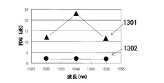
- FIG. 13B shows a change in PDG 1301 in configuration 1211 and a change in PDG 1302 in configuration 1212 when the center wavelengths of incident light are measured at 1530, 1540, and 1550 nm.
- the PDG has a large value of 11.1 to 22.9 dB.
- PDG is 1.2 dB, which is a large reduction compared to the value of the configuration 1211. From this, it was shown that the SOA-PLC hybrid integrated polarization diversity circuit according to this example has an effect of reducing the PDG of the SOA.
Landscapes
- Physics & Mathematics (AREA)
- Engineering & Computer Science (AREA)
- General Physics & Mathematics (AREA)
- Optics & Photonics (AREA)
- Microelectronics & Electronic Packaging (AREA)
- Power Engineering (AREA)
- Optical Integrated Circuits (AREA)
- Optical Modulation, Optical Deflection, Nonlinear Optics, Optical Demodulation, Optical Logic Elements (AREA)
- Semiconductor Lasers (AREA)
Abstract
本願発明は、互いに導波路を結合したPLC-PBSチップとSOA-COSとを備えるSOA-PLCハイブリッド集積偏波ダイバーシティ回路を提供する。PLC-PBSチップは、第1および第2の光導波路と、マッハツェンダー干渉計回路と、TMモードの光が伝播する第1の石英系光導波路中に形成された半波長板とを含む。SOA-COSは、第1の光導波路に接続された第3の光導波路と、第2の光導波路に接続された第4の光導波路と、少なくとも一方の第3および第4の光導波路に形成されたSOAとを含む。第3と第4の光導波路のそれぞれ第1および第2の光導波路と接続しないもう一端同士は、Uターン部光導波路で接続される。
Description
本発明は、平面光波回路(PLC)としての偏波ビームスプリッタ(PBS)および半導体光増幅器(SOA)を備えるSOA-PLCハイブリッド集積偏波ダイバーシティ回路およびその製造方法に関する。
近年、光通信ネットワークにおけるデータ量の増加にともない、コンパクトで低コストである光学素子が要求される。従来の個別の光学部品を組み合わせる技術に代わり、フォトニック集積回路(PIC)技術に基づく光導波路デバイス技術へとトレンドが移行しつつある。
光通信ネットワークにおいて、光導波路デバイスにおける偏波依存性は、実用的に好ましくは、0.1dB以下が要求される。偏波ダイバーシティ回路は、光学デバイスにおける偏波依存性の問題を解消するために使用される。
非特許文献1は、図14のように、それぞれ空間的に分離した個別の光学部品である、3つのポート1401~1403を有するサーキュレータ1409、レンズ1404、偏波ビームスプリッタとしてのハーフミラー1405、半波長板1406、ミラー1407、およびSOA1408を使用した偏波ダイバーシティ回路によりSOAの偏波依存利得(PDG)を解消するための偏波無依存SOAモジュールを開示する。
K. Morito and S. Tanaka, "Record High Saturation Power (+22dBm) and Low Noise Figure (5.7dB) Polarization-Insensitive SOA Module", IEEE PHOTONICS TECHNOLOGY LETTERS, 17, 6, 1298-1300, (2005)
しかしながら、非特許文献1に開示の偏波無依存SOAモジュールは、空間的に分離した個別の光学部品を使用するため、モジュール全体としてサイズが大きくなってしまう。また、非特許文献1に開示の該モジュールでは、ハーフミラー1405やミラー1407等の光学部品が用いられるため、図14に示される該モジュールを形成するには、使用者によるそれぞれの光学部品間の光軸調整が必要であり、非常に手間がかかる。したがって、該モジュールを他のデバイスに組み込む等の応用が難しい。そのため、非特許文献1に開示の該モジュールを商業的に利用することは難しいと考えられる。
本発明の目的は、従来のモジュールに比べモジュール(回路)のサイズを低減し、容易に他のデバイスに組み込むことが可能であるPLC-SOAハイブリッド集積偏波ダイバーシティ回路を提供することである。
本発明は、互いに導波路を結合したPLC-PBSチップとSOA-COSとを備えるSOA-PLCハイブリッド集積偏波ダイバーシティ回路であって、該PLC-PBSチップは、第1および第2の光導波路と、入力された光をTMモードの光およびTEモードの光へ分割し、該分割されたTMモードの光を該第1の光導波路へ出力し、該分割されたTEモードの光を該第2の光導波路へ出力するマッハツェンダー干渉計回路と、該TMモードの光が伝播する第1の石英系光導波路中に形成された偏波回転機構とを含み、該SOA-COSは、該第1の光導波路に接続された第3の光導波路と、該第2の光導波路に接続された第4の光導波路と、少なくとも一方の該第3および第4の光導波路に形成されたSOAとを含み、該第3の光導波路と、該第4の光導波路のそれぞれ該第1の光導波路および該第2の光導波路と接続しないもう一端同士は、Uターン部光導波路で接続されていることを特徴とするSOA-PLCハイブリッド集積偏波ダイバーシティ回路を提供する。
本発明にかかるPLC-SOAハイブリッド集積偏波ダイバーシティ回路は、従来のモジュールに比べモジュール(回路)のサイズを低減することができ、容易に他のデバイスに組み込むことが可能である。
(第1実施形態)
(構成)
図1は、本発明の第1実施形態にかかるSOA-PLCハイブリッド集積偏波ダイバーシティ回路の基本構成を示す模式図である。SOA-PLCハイブリッド集積偏波ダイバーシティ回路100は、石英系平面光波回路-偏波ビームスプリッタ(PLC-PBS)チップ106と半導体光増幅器-チップ・オン・サブマウント(SOA-COS)105とが互いの導波路を結合した構成をとる。
(構成)
図1は、本発明の第1実施形態にかかるSOA-PLCハイブリッド集積偏波ダイバーシティ回路の基本構成を示す模式図である。SOA-PLCハイブリッド集積偏波ダイバーシティ回路100は、石英系平面光波回路-偏波ビームスプリッタ(PLC-PBS)チップ106と半導体光増幅器-チップ・オン・サブマウント(SOA-COS)105とが互いの導波路を結合した構成をとる。
PLC-PBSチップ106は、石英系光導波路109,110と、石英系光導波路が一部切欠した領域であるスリット104と、PBSとしてのマッハツェンダー干渉計回路(MZI)107と、半波長板103とを備える。MZI107は、石英系光導波路としての入力ポート110aおよび出力ポート110b、2つの方向性カプラ111、石英系光導波路としての2つの出力ポート109a、109b、ならびに2つの干渉計アーム(ヒーター)102を有する。なお、MZI107の出力ポート109aからはTMモードの光が出力され、出力ポート109bからはTEモードの光が出力される。半波長板103は、TMモードの光が出力される出力ポート109a部のスリット104に形成される。
SOA-COS105は、直線部108aとUターン部108bを有する半導体光導波路108と、該直線部108aに形成された半導体光増幅器(SOA)112が形成されたSOAチップ113を有する。SOAチップ113はシリコンベンチ114上にハンダ実装される。半導体光導波路の直線部108aは、後述する埋込メサ構造により形成され、半導体光導波路のUターン部108bは後述するハイメサ構造により形成される。このようにすることで、Uターン部108bでは光の閉じ込めを強くすることができ、小さな曲率半径(例えば125μm)の曲線であっても曲げによる光損失を抑制することが可能になる。したがって、光増幅特性および雑音特性の両方を良好にすることができる。ただし、半導体光導波路の直線部108aおよび半導体光導波路のUターン部108bの両方をハイメサ構造または埋込構造とすることもできる。
SOA-COS105が半導体光導波路のUターン部108bを有することで、SOA112の出入力ポート108aaおよび出入力ポート108abが、SOA-COS105のPLC-PBSチップ106側に形成される。すなわち、Uターン部108bを形成することにより、SOA-COS105の同一の端面において光の入力および出力を行うことができ、回路全体のサイズを低減することができる。
本実施形態において、SOA112は半導体光導波路の直線部108aに二箇所形成しているが、SOA112の長さが十分な光増幅効果が得られる長さであれば、SOA112を一箇所に形成してもよい。
図2は、PLC-PBSチップ106とSOA-COS105との接合部付近を詳細に示した平面図である。具体的には、図2は、PLC-PBSチップ106において、MZI107の出力ポート109a、出力ポート109b、スリット104、およびスリット104に形成された半波長板103を示す。また、図2は、SOA-COS105において、SOA112、SOA112の出入力ポート108aaおよび出入力ポート108ab、シリコンベンチ114、SOAチップ113、並びに、半導体光導波路の直線部108aとUターン部108bを示す。
図3Aは、図2に示されるA-A’線に沿ったPLC-PBSチップ106の断面図を示す。PLCプラットフォーム304上に、石英系の下部クラッド層303、石英系光導波路109aおよび109bを構成するコア層301、および上部クラッド層302が形成されている。
図3Bは、PLC-PBSチップ106のスリット104付近を図2に示されるA”方向から見た断面図である。コア層301を伝播する光がスリット104により反射されて生じる伝播ロスと反射戻り光を低減するために、スリット104は、図3Bに示されるように、PLC-PBSチップ106の上部表面に対して垂直に形成されるのではなく所定の角度をもって形成される。例えば、スリット104の幅は20~80μm程度、上部表面の垂線に対して5~12°程度の傾斜を有する。
図4は、図2に示されるB-B’線に沿ったSOA-COS105の半導体光導波路のUターン部108bの断面図を示す。SOA-COS105は、シリコンベンチ114上に、SOAチップ113を実装した形態となっている。SOAチップ113は、下部クラッド層403、半導体光導波路のUターン部108bを構成するコア層402、および上部クラッド層401が形成されたハイメサ構造が使用される。
SOA-COS105は化合物半導体InP基板上にマイクロプロセスで形成される。下部クラッド層403はInPにより形成される。コア層402は化合物半導体InGaAsPにより形成される。そして、上部クラッド層401はInPにより形成される。なお、本実施形態ないし下記の実施形態にかかるSOA-COS105は、InP以外の半導体材料で形成することもできる。また、本実施形態にかかる導波路チップはSOAのような半導体光導波路に限定されない。LiNbO3光導波路やシリコン系光導波路など、偏波依存性をもつすべての導波路に適用することが可能である。
ここで、一般的に、石英系PLCの光導波路では、光導波路を構成するコアとクラッドの比屈折率差は大きくても2.5%程度である。化合物半導体InP等で形成された半導体光導波路では、コアとクラッドの比屈折率差が4~5%を超える。本実施形態では、図4に示されるように、Uターン型の半導体光導波路(Uターン部108b)をハイメサ構造とすることにより、コア層402とその両側の誘電体または空気との比屈折率差が、例えば30~40%以上と非常に大きくなる。また、光導波路を折り返した際の折り返し部の曲率半径は、コアとクラッドの比屈折率差が大きいほど小さくすることができる。例えば、本実施形態において、該曲率半径は125μm程度である。そのため、石英系PLCチップ上でUターン型の光導波路の折り返し構造を形成する場合に比べて、SOA-COS105上でハイメサ構造によってUターン型の光導波路の折り返し構造を形成する方がチップのサイズを小さくすることができる。本実施形態では、Uターン部108bを半導体光導波路として形成し、さらにハイメサ構造とすることにより、Uターン部108bのサイズを小さくすることができ、その結果、回路全体のサイズを小さくすることができる。
SOA112は、半導体光導波路の直線部108aに埋込メサ構造により形成される。SOA112のコア層は光増幅媒質で形成された活性層(図示せず)を有する。SOA112は、注入電流をオン/オフさせることで、入射光をオン/オフさせる半導体ゲートとして用いることもできる。なお、一般的にSOA112の長さが短すぎると所望の利得が得られず、また、長すぎると伝播する光にノイズが入りやすく雑音特性が悪化する。そのため、好ましい例としては、SOA112の長さは例えば0.5~2ミリメートル程度である。
図1に示されたように、本実施形態にかかるSOA-PLCハイブリッド集積偏波ダイバーシティ回路では、PLC-PBSチップ106の石英系光導波路109とSOA-COS105の半導体光導波路の直線部108aとが調芯され、接合されている。
SOA-COS105のSOAチップ113は、PLC-PBSチップ106に比べ薄い。そのため、SOAチップ113をシリコンベンチ114に実装する。このようにすることで、PLC-PBSチップ106とSOA-COS105を接合するときの、接合部分の面積を広くすることが可能になり、PLC-PBSチップ106とSOA-COS105の接合に、十分な強度を得ることができる。
本実施形態においては、図5Aに示されるように、PLC-PBSチップ106とSOA-COS105は、チップごとに導波路の結合を行っている。さらに、本実施形態では、図5Bに示されるように、ベースのシリコン基板501をそれぞれのチップで共有するシリコン基板テラス構造を用いることもできる。この形態においても、ベースのシリコン基板501は共有されているが、PLC-PBSチップ106とSOA-COS105はそれぞれの導波路が結合している。下記の全ての実施形態においても、この導波路結合の形態は適用可能である。
(作用)
本実施形態にかかるSOA-PLCハイブリッド集積偏波ダイバーシティ回路において、入力INからの非偏光の光が、サーキュレータ101によってSOA-PLCハイブリッド集積偏波ダイバーシティ回路100へ伝播される。SOA-PLCハイブリッド集積偏波ダイバーシティ回路100からの光は、サーキュレータ101によって出力OUTに伝播される。
本実施形態にかかるSOA-PLCハイブリッド集積偏波ダイバーシティ回路において、入力INからの非偏光の光が、サーキュレータ101によってSOA-PLCハイブリッド集積偏波ダイバーシティ回路100へ伝播される。SOA-PLCハイブリッド集積偏波ダイバーシティ回路100からの光は、サーキュレータ101によって出力OUTに伝播される。
一般的に、マッハツェンダー干渉計回路(MZI)は2本のアーム間にΔΦの位相差を有する。MZIアーム中で複屈折が起こる場合、TEモードおよびTMモードでの該位相差はそれぞれ独立して変化する。TEモードの該位相差ΔΦTEとTMモードの該位相差ΔΦTMとの差は、|ΔΦTE-ΔΦTM|=(2π/λ)B・Lで表される。ここで、λは波長、BはMZI中の複屈折率、LはMZIのアーム長である。|ΔΦTE-ΔΦTM|が(2n+1)π(n:整数)であるとき、MZIは入射された非偏光の光を2つの直交する光モード(即ち、TEモードとTMモード)へ分割する。そして、TEモードの光は一方の出力ポートへ出力され、TMモードの光は他方の出力ポートへ出力される。
サーキュレータ101から伝播された非偏光の光は、MZI107によって互いに2つの直交モード(即ち、TEモードおよびTMモード)に分けられる。本実施形態にかかる構成においては、MZI107から出射されたTEモードの光は出力ポート109bへ伝播され、TMモードの光は出力ポート109aへ伝播される。出力ポート109aから出力したTMモードの光は、半波長板103によってTEモードの光に変更される。その結果、SOA-COS105にはTEモードの光のみが伝播される。
一般的な半導体光増幅器は、例えば5量子井戸構造であり、12dBの飽和パワー、並びに概ね4dB以下の低い雑音指数を有する。半導体光増幅器自体の偏波依存利得は概ね10~20dB程度である。半導体光増幅器に入射する光について、TEモードの光は19dB程度の小さい信号利得を有するが、TMモードの光は吸収され、-10~0dB程度の利得を有する。
したがって、本実施形態のようにSOA-COS105にTEモードの光のみを伝播することにより、大きな利得を得ることができる上、SOA112の偏波依存利得(PDG)を低減することができる。
したがって、本実施形態のようにSOA-COS105にTEモードの光のみを伝播することにより、大きな利得を得ることができる上、SOA112の偏波依存利得(PDG)を低減することができる。
上記のように、従来の偏波無依存SOAモジュールでは、空間的に分離した個別の光学部品を使用するため、モジュール全体としてサイズが比較的大きくなること、また、ハーフミラー等の光学部品が用いられるため使用者による光学部品間の光軸調整に手間がかかること等の理由から、該モジュールを大量生産し、他のデバイスに組み込む等の応用が難しいという問題があった。
しかしながら、第1実施形態では、SOA-COS105にUターン部108bを設けてSOA-COS105の一端面から光の入出力を可能にし、偏波を分離し、該分離した偏波を統一するように構成されたPLC-PBSチップ106にSOA-COS105に対する入力光および出力光の双方を導波するようにPLC-SOAハイブリッド集積偏波ダイバーシティ回路を構成している。従って、従来のように、SOAへの入力経路と出力経路とを別個に設ける必要がなく、従来の偏波無依存SOAモジュールに比べ、モジュール(回路)のサイズを低減することができる。
また、本実施形態では、ハーフミラー、レンズといった光学部品を用いず、PBSとしてのMZI107、および該MZI107のTMモード出力側の導波路に形成された半波長板103を有する平面光波回路としてのPLC-PBSチップ106を用いているので、使用者による光軸調整の煩わしさを必要としない。
さらに、本実施形態では、偏波ダイバーシティ回路の構成要素であるPLC-PBSチップ106に対する設計マスクを一度作製してしまえば、従来からある半導体集積回路技術や平面光波回路技術を用いて大量生産が可能である。
そして、本実施形態では、導波路チップであるSOA-COS105およびPLC-PBSチップ106の導波路を結合することで、単一の導波路デバイスを形成しているので、他のデバイスに組み込む等の応用が容易である。したがって、該回路は、商業的利用に非常に効果的である。
また、本実施形態では、SOA-COS105にTEモードの光のみを伝播するため、SOA112の偏波依存利得(PDG)を低減することができる。
(製造方法)
PLC-PBSチップ106では、シリコンや石英などの基板上に微細加工技術を組み合わせて、石英系の材料で光導波路が形成される。
PLC-PBSチップ106では、シリコンや石英などの基板上に微細加工技術を組み合わせて、石英系の材料で光導波路が形成される。
一般的に、平面光波回路(PLC)は、光ファイバ製造技術の応用である火炎直接堆積(FHD)法により、PLC基板(例えばシリコン基板)上に下部クラッド層およびコア層となるガラス粒子を堆積し加熱してガラス膜を溶融透明化する。この後、半導体集積回路製造技術であるフォトリソグラフィと反応性イオンエッチングで所望の光導波路パターンを形成し、再びFHD法により上部クラッドを形成する。
複屈折は、石英系ガラス導波路に、局所的に加熱すること、またはUV照射することによりトリミングできる。適切に複屈折をトリミングすることで、石英系PLCチップに偏波ビームスプリッタ(PBS)が形成できる。
ヒーター102は、MZI107における複屈折をトリミングするために、MZI107の2つのアーム上に形成される。ヒーター102でトリミングする間に、MZIの2つのアームの位相差が適切になるように測定される。PLC-PBSチップ106が、所定の光の波長(例えば、1530nm)において、所定の値(例えば、15dB)の偏光消光比を有するように設定される。
図1に示されるように、半波長板103を形成するために、スリット104は、MZI107の2つの出力ポートとSOA-COS105との間に、石英系光導波路109と垂直に交わるように形成される。なお、スリット104は、ダイサー等を用いて形成され、図3Bに示されるように、光が反射するのを防ぐために、PLC-PBSチップ106の上面に対して所定の角度の傾斜をつけて形成される。
本実施形態にかかるSOA-PLCハイブリッド集積偏波ダイバーシティ回路は、PLC-PBSチップ106の石英系光導波路109とSOA-COS105の半導体光導波路の直線部108aとが互いに一つの接触面で接触され、調芯され、接合される。
具体例として、図6を参照して、下記の製造方法のように本実施形態にかかるSOA-PLCハイブリッド集積偏波ダイバーシティ回路を製造する。
(工程1)
図6の符号611に示されるように、石英系光導波路110a、110b、109a、109b、ヒーター102が形成されたPLC-PBSチップ106を準備する。試験光を石英系光導波路110a、110b側から伝播させ、ヒーター102に熱を加え適切にトリミングを行い、MZI107の2つのアームの位相差が適切になるように調整する。
図6の符号611に示されるように、石英系光導波路110a、110b、109a、109b、ヒーター102が形成されたPLC-PBSチップ106を準備する。試験光を石英系光導波路110a、110b側から伝播させ、ヒーター102に熱を加え適切にトリミングを行い、MZI107の2つのアームの位相差が適切になるように調整する。
(工程2)
PLC-PBSチップ106のSOA-COS105が接合されるファセットfPLCを光学研磨によって十分に小さな表面粗さの面に修正する。これにより半導体光導波路の直線部108aおよびUターン部108bと結合するPLC-PBSチップ106の断面が形成される。ダイサー等により、PLC-PBSチップ106の上面に対して垂直ではなく所定の角度をもつようにスリット104を形成する。半波長板103をスリット104中に形成する。半波長板103は、MZI107からTMモードの光を伝播する石英系光導波路側109aに形成する。
PLC-PBSチップ106のSOA-COS105が接合されるファセットfPLCを光学研磨によって十分に小さな表面粗さの面に修正する。これにより半導体光導波路の直線部108aおよびUターン部108bと結合するPLC-PBSチップ106の断面が形成される。ダイサー等により、PLC-PBSチップ106の上面に対して垂直ではなく所定の角度をもつようにスリット104を形成する。半波長板103をスリット104中に形成する。半波長板103は、MZI107からTMモードの光を伝播する石英系光導波路側109aに形成する。
(工程3)
図6の符号612に示されるように、半導体光導波路の直線部108aとUターン部108bおよびSOA112が形成されたSOA-COS105を準備する。SOA-COS105の半導体光導波路の直線部108aを劈開することにより、PLC-PBSチップ106と結合する接合面を形成する。そして、接触する石英系光導波路と半導体光導波路とを調芯し、PLC-PBSチップ106とSOA-COS105とを接着剤などで固定する。
図6の符号612に示されるように、半導体光導波路の直線部108aとUターン部108bおよびSOA112が形成されたSOA-COS105を準備する。SOA-COS105の半導体光導波路の直線部108aを劈開することにより、PLC-PBSチップ106と結合する接合面を形成する。そして、接触する石英系光導波路と半導体光導波路とを調芯し、PLC-PBSチップ106とSOA-COS105とを接着剤などで固定する。
なお、上記工程1~3に含まれる処理内容や工程の順序等は適宜調整してもよい。
上記のSOA-PLCハイブリッド集積偏波ダイバーシティ回路で使用される材料の種類やパラメータ等は単なる例示であり、本実施形態において、ならびに下記の実施形態においても、それらに限定されるものではない。
(第2実施形態)
(構成)
図7は、本発明の第2実施形態にかかるSOA-PLCハイブリッド集積偏波ダイバーシティ回路700の構成を示す模式図である。第2実施形態にかかるSOA-PLCハイブリッド集積偏波ダイバーシティ回路700は、第1実施形態にかかるSOA-PLCハイブリッド集積偏波ダイバーシティ回路100の構成と略同一である。そのため、本実施形態には、第1実施形態にかかるSOA-PLCハイブリッド集積偏波ダイバーシティ回路が有する作用、効果が含まれる。ただし、PLC-PBSチップ106とSOA-COS105との導波路の結合において、モードフィールド径の違いによる光の伝播ロスや導波路の結合面における反射を低減するための構成701が用いられる。
図8Aに構成701の詳細を示す。図8Aに示すように、構成701は、スポットサイズ変換器(SSC)802a、802bを有し、PLC-PBSチップ106とSOA-COS105との接合面f1に対して垂直ではなく所定の角度をもってそれぞれのチップの光導波路が接合されている。
より詳細には、構成701は、コアの中心軸C3を有する直線状の石英系光導波路109a(109b)は、コアの中心軸C1を有する傾斜された石英系光導波路801a(801b)になめらかに接続される。図8Bは、接合面f1における接合部を一部拡大した図である。図8Bに示すように、伝播する光が接合面f1に対して斜めに入射するように、中心軸C1は接合面f1に対して所定の角度θ1傾斜している。同様に、コアの中心軸C2を有する傾斜された半導体光導波路(即ち、SSC802a、802b)は、半導体光導波路の直線部108aになめらかに接続される。傾斜された半導体光導波路であるSSC802a、802bは接合面f1に対して、所定の角度θ2傾斜している。
傾斜された石英系光導波路801a、801bにおける屈折率n1、中心軸C1と接合面f1の垂線とのなす角度θ1、傾斜されたSSC802a、802bにおける屈折率n2、中心軸C2と接合面f1の垂線とのなす角度θ2との間には、スネルの法則より、n1sinθ1=n2sinθ2、という関係がある。この関係を満たすように、傾斜角θ1、θ2が決定される。また、SOA-COS105側の接合面f1上には反射防止(AR)コート803がコーティングされている。なお、PLC側の傾斜角度θ1としては5~9°、半導体導波路側の傾斜角度θ2としては12°~17°が好ましい。
SSC802a、802bは、PLC-PBSチップ106のSOA-COS105の接合面近傍の石英系光導波路801a、801bのモードフィールドと半導体光導波路の直線部108aのモードフィールドとをマッチさせるようにテーパー状の形状を有する光導波路(幅広フレアー型SSC)である。SSC802a、802bは、図8Bに示されるように、部位Aにおける幅を保ったまま部位Bにおいて曲げられ、部位Cにおいてテーパー状に幅が広くなり、部位Dにおいて幅が広がった状態で平行に形成される。本実施形態では、SSC802a、802bは、SOA-COS105の側に形成されているが、PLC-PBSチップ106の側に形成してもよい。SSC802a、802bによって、それぞれの導波路の結合部における結合ロスを低減し、高い結合効率を得ることができる。
(作用)
PLC-PBSチップ106における石英系ガラス等の石英系光導波路の屈折率n1に対して、SOA-COS105におけるInP等の半導体光導波路の屈折率n2は異なるため、それぞれの導波路のモードフィールド(電界分布)が互いに異なる。例えば、石英系光導波路のモードフィールド径は概ね3~8μmであり、InP半導体光導波路のモードフィールド径は概ね1~2μmである。そのため、本実施形態は、PLC-PBSチップ106における石英系光導波路とSOA-COS105の半導体光導波路を結合する際に、モードフィールド径の違いによる光の伝播ロスや接合面における反射を低減するための構成701を用いる。
PLC-PBSチップ106における石英系ガラス等の石英系光導波路の屈折率n1に対して、SOA-COS105におけるInP等の半導体光導波路の屈折率n2は異なるため、それぞれの導波路のモードフィールド(電界分布)が互いに異なる。例えば、石英系光導波路のモードフィールド径は概ね3~8μmであり、InP半導体光導波路のモードフィールド径は概ね1~2μmである。そのため、本実施形態は、PLC-PBSチップ106における石英系光導波路とSOA-COS105の半導体光導波路を結合する際に、モードフィールド径の違いによる光の伝播ロスや接合面における反射を低減するための構成701を用いる。
本実施形態にかかる構成701は、スポットサイズ変換器(SSC)802a、802bを用いてモードフィールド径の違いを修正することができる。また、それぞれのチップの光導波路が所定の角度をもって結合されることで反射を低減することができる。さらに、SOA-COS105側の接合面f1(PLC-PBSチップ106とSOA-COS105との接合面)に反射防止(AR)コート803をコーティングすることで、反射により生じる光の伝播ロスを低減することができる。
本実施形態では、上記のような構成をとることにより、PLC-PBSチップ106における石英系光導波路とSOA-COS105の半導体光導波路を結合する際に、モードフィールド径の違いによる光の伝播ロスや接合面における反射を低減することができる。
図8Aにおいて、光は、石英系光導波路の直線部109aから傾斜された光導波路801a、801bへ入射される。光は、第1実施形態のように接合面f1に対して垂直に入射せず、所定の角度をもって入射される。光は所定の角度で接合面f1へ入射するため、接合面f1による反射光は再度傾斜された光導波路801a、801bへ戻ることは難しい。よって、石英系光導波路109への接合面f1における反射戻り光は低減される。
同様に、光は、SOA-COS105中を伝播しPLC-PBSチップ106へ戻る場合、傾斜された半導体光導波路(即ち、SSC802a、802b)へ入射される。光は、第1実施形態のように接合面f1に対して垂直に入射せず、所定の角度をもって入射される。光は所定の角度で接合面f1へ入射するため、接合面f1による反射光は再度SSC802a、802bへ戻ることは難しい。よって、SSC802a、802bへの接合面f1における反射戻り光は低減される。
(製造方法)
第2実施形態にかかるSOA-PLCハイブリッド集積偏波ダイバーシティ回路の製造方法は、第1実施形態にかかる該回路の製造方法と略同一である。ここで、図9の符号911~913に示される各図には、構成701付近のみを詳細に記載しているが、その他の部分については、第1実施形態にかかる該回路の構成と略同一であるため省略している。
第2実施形態にかかるSOA-PLCハイブリッド集積偏波ダイバーシティ回路の製造方法は、第1実施形態にかかる該回路の製造方法と略同一である。ここで、図9の符号911~913に示される各図には、構成701付近のみを詳細に記載しているが、その他の部分については、第1実施形態にかかる該回路の構成と略同一であるため省略している。
(工程1)
石英系光導波路110、109、SOA-COS105との接合面となるファセットfPLCに垂直な方向に対してある角度θ1だけ水平方向に傾いている石英系光導波路801a、801b、および、ヒーター102が形成されたPLC-PBSチップ106を準備する。試験光を石英系光導波路110側から伝播させ、石英系光導波路109側において、ヒーター102を通過した光を測定する。測定の間、ヒーター102に熱を加え適切にトリミングを行い、MZI107の2つのアームの位相差が適切になるように調整する。
石英系光導波路110、109、SOA-COS105との接合面となるファセットfPLCに垂直な方向に対してある角度θ1だけ水平方向に傾いている石英系光導波路801a、801b、および、ヒーター102が形成されたPLC-PBSチップ106を準備する。試験光を石英系光導波路110側から伝播させ、石英系光導波路109側において、ヒーター102を通過した光を測定する。測定の間、ヒーター102に熱を加え適切にトリミングを行い、MZI107の2つのアームの位相差が適切になるように調整する。
(工程2)
図9の符号911に示されるように、PLC-PBSチップ106の余分な部分を破線Aに沿って切断する。すなわち、石英系光導波路801a、801bは角度θ1の直線部分の任意の点において、ファセットfPLCを形成するように、PLC-PBSチップ106の端部をダイサー等により切断する。切断して形成されるファセットfPLCは光学研磨によって十分に小さな表面粗さの面に修正される。以上により半導体光導波路802a、802bと結合するPLC-PBSチップ106の断面が形成される。ダイサー等によりPLC-PBSチップ106の上面に対して垂直ではなく所定の角度をもつスリット104を形成する。半波長板103をスリット104中に形成する。半波長板103は、MZI107からTMモードの光を伝播する石英系光導波路109a側に形成する。
図9の符号911に示されるように、PLC-PBSチップ106の余分な部分を破線Aに沿って切断する。すなわち、石英系光導波路801a、801bは角度θ1の直線部分の任意の点において、ファセットfPLCを形成するように、PLC-PBSチップ106の端部をダイサー等により切断する。切断して形成されるファセットfPLCは光学研磨によって十分に小さな表面粗さの面に修正される。以上により半導体光導波路802a、802bと結合するPLC-PBSチップ106の断面が形成される。ダイサー等によりPLC-PBSチップ106の上面に対して垂直ではなく所定の角度をもつスリット104を形成する。半波長板103をスリット104中に形成する。半波長板103は、MZI107からTMモードの光を伝播する石英系光導波路109a側に形成する。
(工程3)
図9の符号912に示されるように、半導体光導波路の直線部108a、テーパー状の半導体光導波路である所定の角度(接合面f1の垂線と中心軸C2とのなす角度がθ2となるように)に傾斜されたSSC802a、802b、およびSOA112が形成されたSOA-COS105を準備する。SOA-COS105は、半導体光導波路802a、802bの出射角度がθ2になるように劈開され、PLC-PBSチップ106と結合するSOA-COS105のファセットfSOAが形成される。半導体光導波路の直線部108aとSOA112は埋込メサ構造により形成され、半導体光導波路のUターン部108bはハイメサ構造により形成されており、SOA-COS105のファセットfSOAにARコート803がコーティングされている。
図9の符号912に示されるように、半導体光導波路の直線部108a、テーパー状の半導体光導波路である所定の角度(接合面f1の垂線と中心軸C2とのなす角度がθ2となるように)に傾斜されたSSC802a、802b、およびSOA112が形成されたSOA-COS105を準備する。SOA-COS105は、半導体光導波路802a、802bの出射角度がθ2になるように劈開され、PLC-PBSチップ106と結合するSOA-COS105のファセットfSOAが形成される。半導体光導波路の直線部108aとSOA112は埋込メサ構造により形成され、半導体光導波路のUターン部108bはハイメサ構造により形成されており、SOA-COS105のファセットfSOAにARコート803がコーティングされている。
(工程4)
図9の符号913に示されるように、それぞれのチップの光導波路を調芯し、それぞれのチップを接着剤などで固定する。導波路の接合面f1はPLC-PBSチップ側のファセットfPLCとSOA-COS側のファセットfSOAの2つが対向して、石英系光導波路801aと半導体導波路802a、石英系光導波路801bと半導体導波路802bがそれぞれ光学的に結合する空間で形成される。なお、上記工程1~4に含まれる処理内容や工程の順序等は適宜調整してもよい。
図9の符号913に示されるように、それぞれのチップの光導波路を調芯し、それぞれのチップを接着剤などで固定する。導波路の接合面f1はPLC-PBSチップ側のファセットfPLCとSOA-COS側のファセットfSOAの2つが対向して、石英系光導波路801aと半導体導波路802a、石英系光導波路801bと半導体導波路802bがそれぞれ光学的に結合する空間で形成される。なお、上記工程1~4に含まれる処理内容や工程の順序等は適宜調整してもよい。
(第3実施形態)
(構成)
図10は、本発明の第3実施形態にかかるSOA-PLCハイブリッド集積偏波ダイバーシティ回路1000の構成を示す模式図である。第3実施形態にかかるSOA-PLCハイブリッド集積偏波ダイバーシティ回路1000は、第1実施形態および第2実施形態にかかるSOA-PLCハイブリッド集積偏波ダイバーシティ回路の構成と略同一である。そのため、本実施形態には、第1実施形態および第2実施形態にかかるSOA-PLCハイブリッド集積偏波ダイバーシティ回路が有する作用、効果が含まれる。ただし、本実施形態においては、SOA-COS1001に光導波路の折り返し部を形成するのではなく、UターンPLCチップ1002にUターン状の石英系光導波路1003を形成し、SOA112により増幅した光をMZI107へ戻すようにしている。そして、SOA112はSOA-COS1001の半導体光導波路の直線部に形成されている。すなわち、第3実施形態においては、PLC-PBSチップ106から伝播された光は、SOA-COS1001に形成されたSOA112で増幅され、UターンPLCチップ1002に形成されたUターン石英系光導波路1003で折り返され、再びSOA-COS1001に形成されたSOA112で増幅され、PLC-PBSチップ106へ戻る。
本実施形態にかかるSOA-PLCハイブリッド集積偏波ダイバーシティ回路においても、PLC-PBSチップ105とSOA-COS1001との接合部およびSOA-COS1001とUターンPLCチップ1002との接合部におけるそれぞれのチップの光導波路は、第2実施形態にかかる該回路の特徴のように、コアサイズの違いによる光の伝播ロスや接合面における反射を低減するための構成701を用いている。
(作用)
上記したように、大きい比屈折率差の光導波路であるほど折り返し部の曲率半径を小さくすることができ、その結果、回路全体のサイズを低減することができる。しかしながら、第2実施形態にかかるSOA-PLCハイブリッド集積偏波ダイバーシティ回路のように、SOAに適した埋込メサ構造の半導体導波路と、曲率半径の小さいUターンに適したハイメサ構造の半導体導波路を結合して同じチップ内で作製することは、必ずしも容易ではない。
上記したように、大きい比屈折率差の光導波路であるほど折り返し部の曲率半径を小さくすることができ、その結果、回路全体のサイズを低減することができる。しかしながら、第2実施形態にかかるSOA-PLCハイブリッド集積偏波ダイバーシティ回路のように、SOAに適した埋込メサ構造の半導体導波路と、曲率半径の小さいUターンに適したハイメサ構造の半導体導波路を結合して同じチップ内で作製することは、必ずしも容易ではない。
Uターン構造をなくし、埋込メサ構造の半導体導波路のみでSOA-COSを構成するほうが、容易に導波路を形成することができる。第2実施形態のSOA-PLCハイブリッド集積偏波ダイバーシティ回路に比べ、本実施形態にかかるSOA-PLCハイブリッド集積偏波ダイバーシティ回路は、全体のサイズが少し大きくなるが、SOA-COSの作製が容易になり、偏波ダイバーシティ回路の実現性が高まる。
(製造方法)
第3実施形態にかかるSOA-PLCハイブリッド集積偏波ダイバーシティ回路の製造方法は、第1実施形態および第2実施形態にかかる該回路の製造方法と略同一である。ここで、図8の各図には、PLC-PBSチップ106、SOA-COS1001およびUターンPLCチップ1002の接合部における構成701付近のみを詳細に記載している。その他の部分については、第1実施形態および第2実施形態にかかる該回路の構成と略同一であるため省略している。
第3実施形態にかかるSOA-PLCハイブリッド集積偏波ダイバーシティ回路の製造方法は、第1実施形態および第2実施形態にかかる該回路の製造方法と略同一である。ここで、図8の各図には、PLC-PBSチップ106、SOA-COS1001およびUターンPLCチップ1002の接合部における構成701付近のみを詳細に記載している。その他の部分については、第1実施形態および第2実施形態にかかる該回路の構成と略同一であるため省略している。
(工程1)
石英系光導波路110、109、所定の角度に傾斜された石英系光導波路801a、801b、ヒーター102が形成されたPLC-PBSチップ106を準備する。試験光を石英系光導波路110側から伝播させ、石英系光導波路109側において、ヒーター102を通過した光を測定する。測定の間、ヒーター102に熱を加え適切にトリミングを行い、MZI107の2つのアームの位相差が適切になるように調整する。また、Uターン状の石英系光導波路1003、石英系光導波路109、所定の角度に傾斜された石英系光導波路801a、801bが形成されたUターンPLCチップ1002を準備する。
石英系光導波路110、109、所定の角度に傾斜された石英系光導波路801a、801b、ヒーター102が形成されたPLC-PBSチップ106を準備する。試験光を石英系光導波路110側から伝播させ、石英系光導波路109側において、ヒーター102を通過した光を測定する。測定の間、ヒーター102に熱を加え適切にトリミングを行い、MZI107の2つのアームの位相差が適切になるように調整する。また、Uターン状の石英系光導波路1003、石英系光導波路109、所定の角度に傾斜された石英系光導波路801a、801bが形成されたUターンPLCチップ1002を準備する。
(工程2)
図11の符号1111に示されるように、PLC-PBSチップ106およびUターンPLCチップ1002の余分な部分を破線AおよびA’に沿って切断する。すなわち、石英系光導波路801a、801bは角度θ1の直線部分の任意の点において、ファセットfPLCを形成するように、PLC-PBSチップ106およびUターンPLCチップ1002の端部をダイサー等により切断する。切断して形成されるファセットfPLCは光学研磨によって十分に小さな表面粗さの面に修正される。以上により半導体光導波路802a、802bと結合するPLC-PBSチップ106、およびUターンPLCチップ1002の断面が形成される。また、ダイサー等によりPLC-PBSチップ106の上面に対して垂直ではなく所定の角度をもつスリット104を形成する。半波長板103をスリット104中に形成する。半波長板103は、MZI107からTMモードの光を伝播する石英系光導波路109a側に形成する。
図11の符号1111に示されるように、PLC-PBSチップ106およびUターンPLCチップ1002の余分な部分を破線AおよびA’に沿って切断する。すなわち、石英系光導波路801a、801bは角度θ1の直線部分の任意の点において、ファセットfPLCを形成するように、PLC-PBSチップ106およびUターンPLCチップ1002の端部をダイサー等により切断する。切断して形成されるファセットfPLCは光学研磨によって十分に小さな表面粗さの面に修正される。以上により半導体光導波路802a、802bと結合するPLC-PBSチップ106、およびUターンPLCチップ1002の断面が形成される。また、ダイサー等によりPLC-PBSチップ106の上面に対して垂直ではなく所定の角度をもつスリット104を形成する。半波長板103をスリット104中に形成する。半波長板103は、MZI107からTMモードの光を伝播する石英系光導波路109a側に形成する。
(工程3)
図11の符号1112に示されるように、半導体光導波路の直線部108a、テーパー状の半導体光導波路である傾斜されたSSC802a、802b、およびSOA112が形成されたSOA-COS1001を準備する。SOA-COS1001は、半導体光導波路802a、802bの出射角度がθ2(図8B参照)になるように劈開され、PLC-PBSチップ106およびUターンPLCチップ1002と結合するSOA-COS1001のファセットfSOAが形成される。その後、SOA-COS1001の両方の切断面であるファセットfSOAにARコート803(図8B参照)をコーティングする。
図11の符号1112に示されるように、半導体光導波路の直線部108a、テーパー状の半導体光導波路である傾斜されたSSC802a、802b、およびSOA112が形成されたSOA-COS1001を準備する。SOA-COS1001は、半導体光導波路802a、802bの出射角度がθ2(図8B参照)になるように劈開され、PLC-PBSチップ106およびUターンPLCチップ1002と結合するSOA-COS1001のファセットfSOAが形成される。その後、SOA-COS1001の両方の切断面であるファセットfSOAにARコート803(図8B参照)をコーティングする。
(工程4)
図11の符号1113に示されるように、それぞれのチップの光導波路を調芯し、それぞれのチップを接着剤などで固定する。導波路の接合面f1はPLC-PBSチップおよびUターンPLCチップ側のファセットfPLCとSOA-COS側のファセットfSOAの2つが対向して、石英系光導波路801aと半導体導波路802a、および、石英系光導波路801bと半導体導波路802bがそれぞれ光学的に結合する空間で形成される。
なお、上記工程1~4に含まれる処理内容や工程の順序等は適宜調整してもよい。
図11の符号1113に示されるように、それぞれのチップの光導波路を調芯し、それぞれのチップを接着剤などで固定する。導波路の接合面f1はPLC-PBSチップおよびUターンPLCチップ側のファセットfPLCとSOA-COS側のファセットfSOAの2つが対向して、石英系光導波路801aと半導体導波路802a、および、石英系光導波路801bと半導体導波路802bがそれぞれ光学的に結合する空間で形成される。
なお、上記工程1~4に含まれる処理内容や工程の順序等は適宜調整してもよい。
(実施例)
図12は、SOAの偏波依存利得(PDG)を測定するために、2種類のPDG測定構成を示す。図12は、調整可能な光源(TLS)1201、エルビウム添加光ファイバ増幅器(EDFA)1202、偏波コントローラ(PC)1203、減衰器(ATT)1204、入力側光スイッチ1205、光スペクトラムアナライザ(OSA)1206、光パワーメータ(OPM)1207、10:1スプリッタ1208、アイソレータ1209、出力側光スイッチ1210、基準構成1211、および第3実施形態にかかるSOA-PLCハイブリッド集積偏波ダイバーシティ回路構成1212を示す。構成1211は、2つのストレート型光導波路を有するST-PLCチップとSOAを有するSOA-COS、ならびにUターン型光導波路を有するU-PLCチップとが接合された構成をとる。構成1211は、構成1212に比べ、サーキュレータと偏波ビームスプリッタを有しない。
図12は、SOAの偏波依存利得(PDG)を測定するために、2種類のPDG測定構成を示す。図12は、調整可能な光源(TLS)1201、エルビウム添加光ファイバ増幅器(EDFA)1202、偏波コントローラ(PC)1203、減衰器(ATT)1204、入力側光スイッチ1205、光スペクトラムアナライザ(OSA)1206、光パワーメータ(OPM)1207、10:1スプリッタ1208、アイソレータ1209、出力側光スイッチ1210、基準構成1211、および第3実施形態にかかるSOA-PLCハイブリッド集積偏波ダイバーシティ回路構成1212を示す。構成1211は、2つのストレート型光導波路を有するST-PLCチップとSOAを有するSOA-COS、ならびにUターン型光導波路を有するU-PLCチップとが接合された構成をとる。構成1211は、構成1212に比べ、サーキュレータと偏波ビームスプリッタを有しない。
TLS1201から構成1211に光を入射する場合、該構成1211はPDCを用いないため、構成1211を伝播する光はそのまま、入力側光スイッチ1205から出力側光スイッチ1210へと一方向に伝播する。構成1211におけるSOAのPDGを調べるために、TLS1201からTEモードの光(中心波長λ=1550nm)を入射させた場合の測定結果を図13Aの符号1311に示すグラフに、TLS1201からTMモードの光を入射させた場合の測定結果を図13Aの符号1312に示すグラフに示す。なお、図13Aの符号1311~1314に示すグラフのスケールは、横軸が1549.5~1550~1550.5(nm)、縦軸が-60~0~+10(dBm)であり、上側の太線のスペクトルが構成1211および構成1212を通過後の出力光のスペクトル、下側のスペクトルが入力光のスペクトルである。
また、構成1212におけるSOAのPDGを調べるために、TLS1201からTEモードの光(中心波長λ=1550nm)を入射させた場合の測定結果を図13Aの符号1313に示すグラフに、TLS1201からTMモードの光を入射させた場合の測定結果を図13Aの符号1314に示すグラフに示す。なお、構成1212において、上記θ1を15°、θ2を7°とすることで、伝播光のリターンロスは-50dB以下に低減された。
構成1211において、TEモードの光の場合は、5.8dBの増幅利得が得られたが、TMモードの光の場合は、-5.3dBと負の増幅利得が得られた。構成1212において、TEモードの光の場合は、6.3dBの増幅利得が得られ、TMモードの光の場合は、4.4dBの増幅利得が得られた。
この結果から、TEモードの光は、構成1211および構成1212にかかわらず、即ちPDCの構成を有するか否かにかかわらず、SOAによる光増幅利得が得られた。しかしながら、TMモードの光について、構成1212ではSOAによる光増幅利得が得られたが、構成1211ではSOAによる負の光増幅利得(即ち、吸収)が得られた。
よって、構成1211の偏波依存利得(PDG)は11.1dBであった。一方、構成1212のPDGは1.9dBであった。本発明の第3実施形態にかかるSOA-PLCハイブリッド集積偏波ダイバーシティ回路(構成1212)を用いることで、PDGを大きく低減できた。
図13Bに、入射光の中心波長を1530、1540、1550nmで測定した場合における、構成1211のPDG1301の変化および構成1212のPDG1302の変化を示す。構成1211では、PDGが11.1~22.9dBと大きい値をとった。一方、構成1212では、PDGが1.2dBと構成1211の値に比べ大きく低減した。このことから、本実施例にかかるSOA-PLCハイブリッド集積偏波ダイバーシティ回路は、SOAのPDGを低減するという効果があることが示された。
Claims (7)
- 互いに導波路を結合したPLC-PBSチップとSOA-COSとを備えるSOA-PLCハイブリッド集積偏波ダイバーシティ回路であって、
前記PLC-PBSチップは、
第1および第2の光導波路と、
入力された光をTMモードの光およびTEモードの光へ分割し、前記分割されたTMモードの光を前記第1の光導波路へ出力し、前記分割されたTEモードの光を前記第2の光導波路へ出力するマッハツェンダー干渉計回路と、
前記TMモードの光が伝播する第1の光導波路中に形成された偏波回転機構とを含み、
前記SOA-COSは、
前記第1の光導波路に接続された第3の光導波路と、
前記第2の光導波路に接続された第4の光導波路と、
少なくとも一方の前記第3および第4の光導波路に形成されたSOAとを含み、
前記第3の光導波路と、前記第4の光導波路のそれぞれ前記第1の光導波路および前記第2の光導波路と接続しないもう一端同士は、Uターン部光導波路で接続されていることを特徴とするSOA-PLCハイブリッド集積偏波ダイバーシティ回路。 - 前記Uターン部光導波路は、前記SOA-COS上に形成されていることを特徴とする請求項1に記載のSOA-PLCハイブリッド集積偏波ダイバーシティ回路。
- 前記第1および第2の光導波路が埋込メサ構造を有し、前記Uターン部光導波路がハイメサ構造を有することを特徴とする請求項2に記載のSOA-PLCハイブリッド集積偏波ダイバーシティ回路。
- 前記SOA-COSと導波路を結合したUターンPLCチップをさらに備え、前記Uターン部光導波路は、前記UターンPLCチップ上に形成されていることを特徴とする請求項1に記載のSOA-PLCハイブリッド集積偏波ダイバーシティ回路。
- 2つのチップの接合面において、前記第1から第4の光導波路の少なくとも1つの光導波路がスポットサイズ変換器を含むことを特徴とする請求項1から4のいずれか1に記載のSOA-PLCハイブリッド集積偏波ダイバーシティ回路。
- 2つのチップの接合面において、接合される前記光導波路が接合面に対していずれも傾斜を有し、
前記傾斜された光導波路同士がが、前記接合面に対してそれぞれ第1の角度および第2の角度を有して接合されていることを特徴とする請求項1から4のいずれか1に記載のSOA-PLCハイブリッド集積偏波ダイバーシティ回路。 - 2つのチップの接合面に、反射防止コートが形成されていることを特徴とする請求項1から6のいずれか1に記載のSOA-PLCハイブリッド集積偏波ダイバーシティ回路。
Priority Applications (1)
| Application Number | Priority Date | Filing Date | Title |
|---|---|---|---|
| US13/735,601 US8837869B2 (en) | 2011-02-03 | 2013-01-07 | SOA-PLC hybrid integrated polarization diversity circuit and method for manufacturing the same |
Applications Claiming Priority (2)
| Application Number | Priority Date | Filing Date | Title |
|---|---|---|---|
| JP2011021814A JP2012163614A (ja) | 2011-02-03 | 2011-02-03 | Soa−plcハイブリッド集積偏波ダイバーシティ回路およびその製造方法 |
| JP2011-021814 | 2011-02-03 |
Related Child Applications (1)
| Application Number | Title | Priority Date | Filing Date |
|---|---|---|---|
| US13/735,601 Continuation US8837869B2 (en) | 2011-02-03 | 2013-01-07 | SOA-PLC hybrid integrated polarization diversity circuit and method for manufacturing the same |
Publications (1)
| Publication Number | Publication Date |
|---|---|
| WO2012105247A1 true WO2012105247A1 (ja) | 2012-08-09 |
Family
ID=46602470
Family Applications (1)
| Application Number | Title | Priority Date | Filing Date |
|---|---|---|---|
| PCT/JP2012/000662 Ceased WO2012105247A1 (ja) | 2011-02-03 | 2012-02-01 | Soa-plcハイブリッド集積偏波ダイバーシティ回路およびその製造方法 |
Country Status (3)
| Country | Link |
|---|---|
| US (1) | US8837869B2 (ja) |
| JP (1) | JP2012163614A (ja) |
| WO (1) | WO2012105247A1 (ja) |
Families Citing this family (14)
| Publication number | Priority date | Publication date | Assignee | Title |
|---|---|---|---|---|
| FR2986082B1 (fr) * | 2012-01-19 | 2015-08-21 | Ixblue | Circuit optique integre a zone d'attenuation traversante |
| JP5567226B2 (ja) | 2012-05-31 | 2014-08-06 | 古河電気工業株式会社 | 半導体レーザモジュール |
| US9577410B2 (en) * | 2013-02-01 | 2017-02-21 | Nec Corporation | Optical functional integrated unit and method for manufacturing thereof |
| JP5837015B2 (ja) * | 2013-09-30 | 2015-12-24 | 沖電気工業株式会社 | 半導体レーザモジュール及びその製造方法 |
| US9762334B2 (en) | 2015-12-31 | 2017-09-12 | Alcatel-Lucent Usa Inc. | Photonic integrated circuit using chip integration |
| CN114342193A (zh) * | 2019-08-02 | 2022-04-12 | 古河电气工业株式会社 | 半导体光放大器阵列元件 |
| CA3163589A1 (en) * | 2020-01-13 | 2021-07-22 | Ours Technology, Llc | Silicon-assisted packaging of high power integrated soa array |
| JP7435273B2 (ja) * | 2020-06-03 | 2024-02-21 | 富士通オプティカルコンポーネンツ株式会社 | 光集積素子、及び光集積回路 |
| JP6910568B1 (ja) * | 2020-07-03 | 2021-07-28 | 三菱電機株式会社 | 半導体光集積素子 |
| JP7884334B2 (ja) * | 2021-12-08 | 2026-07-03 | 古河電気工業株式会社 | ラマン増幅用励起光源、光源装置、ラマン増幅用励起光源の駆動方法、ラマン増幅用励起光源の設計方法、ラマン増幅器、およびラマン増幅システム |
| EP4430713A1 (en) * | 2022-02-23 | 2024-09-18 | Huawei Technologies Co., Ltd. | Dummy light module comprising dual semiconductor optical amplifier |
| US11940567B1 (en) | 2022-12-01 | 2024-03-26 | Aurora Operations, Inc. | Light detection and ranging (LIDAR) sensor system including integrated light source |
| US12066537B2 (en) * | 2022-12-30 | 2024-08-20 | Aurora Operations, Inc | Light detection and ranging (LIDAR) system including high-power amplifier |
| IT202300007764A1 (it) * | 2023-04-20 | 2024-10-20 | Google Llc | Amplificatore ottico insensibile a polarizzazione |
Citations (6)
| Publication number | Priority date | Publication date | Assignee | Title |
|---|---|---|---|---|
| JP2001272560A (ja) * | 2000-03-27 | 2001-10-05 | Fuji Photo Film Co Ltd | 光導波路素子および半導体レーザ装置 |
| JP2002311267A (ja) * | 2001-04-12 | 2002-10-23 | Nippon Telegr & Teleph Corp <Ntt> | 接続型光導波路 |
| JP2003207668A (ja) * | 2002-01-11 | 2003-07-25 | Nippon Telegr & Teleph Corp <Ntt> | 偏波制御回路アレイおよびそれを用いた光回路 |
| JP2005157163A (ja) * | 2003-11-28 | 2005-06-16 | Sumitomo Electric Ind Ltd | 光デバイス |
| WO2006013928A1 (ja) * | 2004-08-04 | 2006-02-09 | The Furukawa Electric Co., Ltd. | 光回路装置 |
| JP2008275708A (ja) * | 2007-04-25 | 2008-11-13 | Keio Gijuku | 偏波制御光回路 |
Family Cites Families (10)
| Publication number | Priority date | Publication date | Assignee | Title |
|---|---|---|---|---|
| JP2902082B2 (ja) * | 1990-08-30 | 1999-06-07 | 沖電気工業株式会社 | 光波長フィルタ及びその駆動方法 |
| KR0162755B1 (ko) * | 1994-12-09 | 1999-04-15 | 양승택 | 고분자 도파로형 광 세기 변조기 |
| JP3006553B2 (ja) * | 1997-07-08 | 2000-02-07 | 日本電気株式会社 | 半導体集積型偏波モード変換器 |
| JP3841933B2 (ja) * | 1997-08-28 | 2006-11-08 | 富士通株式会社 | 光導波路モジュール |
| JP3850569B2 (ja) * | 1998-12-09 | 2006-11-29 | 富士通株式会社 | フェルールアセンブリ及び光モジュール |
| US7315672B2 (en) | 2003-11-28 | 2008-01-01 | Sumitomo Electric Industries, Ltd. | Optical device |
| US7738527B2 (en) * | 2005-12-30 | 2010-06-15 | Jian-Jun He | Wavelength switchable semiconductor laser using half-wave coupled active double-ring resonator |
| US7916984B2 (en) * | 2007-03-16 | 2011-03-29 | Electronics And Telecommunications Research Institute | Opto-electric bus module and method of manufacturing the same |
| WO2009133631A1 (en) * | 2008-04-30 | 2009-11-05 | Nec Corporation | Tunable laser source using intracavity laser light outcoupling and module containing the same |
| JP5182049B2 (ja) * | 2008-12-09 | 2013-04-10 | 富士通株式会社 | 偏波変換デバイス及び偏波多重変調器 |
-
2011
- 2011-02-03 JP JP2011021814A patent/JP2012163614A/ja not_active Withdrawn
-
2012
- 2012-02-01 WO PCT/JP2012/000662 patent/WO2012105247A1/ja not_active Ceased
-
2013
- 2013-01-07 US US13/735,601 patent/US8837869B2/en active Active
Patent Citations (6)
| Publication number | Priority date | Publication date | Assignee | Title |
|---|---|---|---|---|
| JP2001272560A (ja) * | 2000-03-27 | 2001-10-05 | Fuji Photo Film Co Ltd | 光導波路素子および半導体レーザ装置 |
| JP2002311267A (ja) * | 2001-04-12 | 2002-10-23 | Nippon Telegr & Teleph Corp <Ntt> | 接続型光導波路 |
| JP2003207668A (ja) * | 2002-01-11 | 2003-07-25 | Nippon Telegr & Teleph Corp <Ntt> | 偏波制御回路アレイおよびそれを用いた光回路 |
| JP2005157163A (ja) * | 2003-11-28 | 2005-06-16 | Sumitomo Electric Ind Ltd | 光デバイス |
| WO2006013928A1 (ja) * | 2004-08-04 | 2006-02-09 | The Furukawa Electric Co., Ltd. | 光回路装置 |
| JP2008275708A (ja) * | 2007-04-25 | 2008-11-13 | Keio Gijuku | 偏波制御光回路 |
Non-Patent Citations (1)
| Title |
|---|
| KEN MORITO ET AL.: "Record high saturation power (+22 dBm) and low noise figure (5.7 dB) polarization-insensitive SOA module", PHOTONICS TECHNOLOGY LETTERS, vol. 17, no. ISSUE:, June 2005 (2005-06-01), pages 1298 - 1300 * |
Also Published As
| Publication number | Publication date |
|---|---|
| US8837869B2 (en) | 2014-09-16 |
| US20130121632A1 (en) | 2013-05-16 |
| JP2012163614A (ja) | 2012-08-30 |
Similar Documents
| Publication | Publication Date | Title |
|---|---|---|
| US8837869B2 (en) | SOA-PLC hybrid integrated polarization diversity circuit and method for manufacturing the same | |
| Halir et al. | Recent advances in silicon waveguide devices using sub-wavelength gratings | |
| JP7477761B2 (ja) | モード変換素子 | |
| US9054486B2 (en) | Optical amplifier device | |
| US6580850B1 (en) | Optical waveguide multimode to single mode transformer | |
| KR102162833B1 (ko) | 집적된 마하젠더 변조기를 구비한 튜너블 u-레이저 전송기 | |
| JP5323646B2 (ja) | ハイブリッド集積光モジュール | |
| CN106094107B (zh) | 一种偏振分束器 | |
| US20110243494A1 (en) | Semiconductor optical amplifier module | |
| JP3967356B2 (ja) | 光導波路デバイス | |
| CN112346175B (zh) | 一种3dB光波功率分束器 | |
| US10564355B2 (en) | Optical waveguide element | |
| US20120163751A1 (en) | Reflection type optical delay interferometer apparatus based on planar waveguide | |
| WO2012102041A1 (ja) | 導波路型偏波ビームスプリッタ | |
| JP2010020105A (ja) | 光半導体装置及びその製造方法 | |
| CN118103743A (zh) | 具有增加相容性的载流子注入器 | |
| WO2011155391A1 (ja) | 光90度ハイブリッド | |
| Zhu et al. | A polarization insensitive semiconductor optical amplifier | |
| JP6379090B2 (ja) | 光実装デバイス | |
| JP4468397B2 (ja) | 光導波路デバイス | |
| JP2000077771A (ja) | 半導体光増幅装置 | |
| JP7608153B2 (ja) | 光学デバイスおよび光学装置 | |
| JP2018046144A (ja) | 波長可変レーザ、波長可変レーザ装置及びその制御方法 | |
| JP4756011B2 (ja) | 光デバイス | |
| Aalto et al. | Si photonics using micron-size waveguides |
Legal Events
| Date | Code | Title | Description |
|---|---|---|---|
| 121 | Ep: the epo has been informed by wipo that ep was designated in this application |
Ref document number: 12742078 Country of ref document: EP Kind code of ref document: A1 |
|
| NENP | Non-entry into the national phase |
Ref country code: DE |
|
| 122 | Ep: pct application non-entry in european phase |
Ref document number: 12742078 Country of ref document: EP Kind code of ref document: A1 |