WO2012105146A1 - 光電変換装置及び光電変換モジュール - Google Patents
光電変換装置及び光電変換モジュール Download PDFInfo
- Publication number
- WO2012105146A1 WO2012105146A1 PCT/JP2011/080165 JP2011080165W WO2012105146A1 WO 2012105146 A1 WO2012105146 A1 WO 2012105146A1 JP 2011080165 W JP2011080165 W JP 2011080165W WO 2012105146 A1 WO2012105146 A1 WO 2012105146A1
- Authority
- WO
- WIPO (PCT)
- Prior art keywords
- photoelectric conversion
- metal film
- electrode
- film
- conversion module
- Prior art date
- Legal status (The legal status is an assumption and is not a legal conclusion. Google has not performed a legal analysis and makes no representation as to the accuracy of the status listed.)
- Ceased
Links
Images

Classifications
-
- H—ELECTRICITY
- H10—SEMICONDUCTOR DEVICES; ELECTRIC SOLID-STATE DEVICES NOT OTHERWISE PROVIDED FOR
- H10F—INORGANIC SEMICONDUCTOR DEVICES SENSITIVE TO INFRARED RADIATION, LIGHT, ELECTROMAGNETIC RADIATION OF SHORTER WAVELENGTH OR CORPUSCULAR RADIATION
- H10F77/00—Constructional details of devices covered by this subclass
- H10F77/20—Electrodes
- H10F77/206—Electrodes for devices having potential barriers
- H10F77/211—Electrodes for devices having potential barriers for photovoltaic cells
-
- H—ELECTRICITY
- H10—SEMICONDUCTOR DEVICES; ELECTRIC SOLID-STATE DEVICES NOT OTHERWISE PROVIDED FOR
- H10F—INORGANIC SEMICONDUCTOR DEVICES SENSITIVE TO INFRARED RADIATION, LIGHT, ELECTROMAGNETIC RADIATION OF SHORTER WAVELENGTH OR CORPUSCULAR RADIATION
- H10F10/00—Individual photovoltaic cells, e.g. solar cells
- H10F10/10—Individual photovoltaic cells, e.g. solar cells having potential barriers
- H10F10/16—Photovoltaic cells having only PN heterojunction potential barriers
- H10F10/164—Photovoltaic cells having only PN heterojunction potential barriers comprising heterojunctions with Group IV materials, e.g. ITO/Si or GaAs/SiGe photovoltaic cells
- H10F10/165—Photovoltaic cells having only PN heterojunction potential barriers comprising heterojunctions with Group IV materials, e.g. ITO/Si or GaAs/SiGe photovoltaic cells the heterojunctions being Group IV-IV heterojunctions, e.g. Si/Ge, SiGe/Si or Si/SiC photovoltaic cells
- H10F10/166—Photovoltaic cells having only PN heterojunction potential barriers comprising heterojunctions with Group IV materials, e.g. ITO/Si or GaAs/SiGe photovoltaic cells the heterojunctions being Group IV-IV heterojunctions, e.g. Si/Ge, SiGe/Si or Si/SiC photovoltaic cells the Group IV-IV heterojunctions being heterojunctions of crystalline and amorphous materials, e.g. silicon heterojunction [SHJ] photovoltaic cells
-
- H—ELECTRICITY
- H10—SEMICONDUCTOR DEVICES; ELECTRIC SOLID-STATE DEVICES NOT OTHERWISE PROVIDED FOR
- H10F—INORGANIC SEMICONDUCTOR DEVICES SENSITIVE TO INFRARED RADIATION, LIGHT, ELECTROMAGNETIC RADIATION OF SHORTER WAVELENGTH OR CORPUSCULAR RADIATION
- H10F19/00—Integrated devices, or assemblies of multiple devices, comprising at least one photovoltaic cell covered by group H10F10/00, e.g. photovoltaic modules
- H10F19/90—Structures for connecting between photovoltaic cells, e.g. interconnections or insulating spacers
- H10F19/902—Structures for connecting between photovoltaic cells, e.g. interconnections or insulating spacers for series or parallel connection of photovoltaic cells
- H10F19/906—Structures for connecting between photovoltaic cells, e.g. interconnections or insulating spacers for series or parallel connection of photovoltaic cells characterised by the materials of the structures
-
- H—ELECTRICITY
- H10—SEMICONDUCTOR DEVICES; ELECTRIC SOLID-STATE DEVICES NOT OTHERWISE PROVIDED FOR
- H10F—INORGANIC SEMICONDUCTOR DEVICES SENSITIVE TO INFRARED RADIATION, LIGHT, ELECTROMAGNETIC RADIATION OF SHORTER WAVELENGTH OR CORPUSCULAR RADIATION
- H10F77/00—Constructional details of devices covered by this subclass
- H10F77/20—Electrodes
- H10F77/206—Electrodes for devices having potential barriers
- H10F77/211—Electrodes for devices having potential barriers for photovoltaic cells
- H10F77/215—Geometries of grid contacts
-
- H—ELECTRICITY
- H10—SEMICONDUCTOR DEVICES; ELECTRIC SOLID-STATE DEVICES NOT OTHERWISE PROVIDED FOR
- H10F—INORGANIC SEMICONDUCTOR DEVICES SENSITIVE TO INFRARED RADIATION, LIGHT, ELECTROMAGNETIC RADIATION OF SHORTER WAVELENGTH OR CORPUSCULAR RADIATION
- H10F77/00—Constructional details of devices covered by this subclass
- H10F77/40—Optical elements or arrangements
- H10F77/42—Optical elements or arrangements directly associated or integrated with photovoltaic cells, e.g. light-reflecting means or light-concentrating means
- H10F77/48—Back surface reflectors [BSR]
-
- Y—GENERAL TAGGING OF NEW TECHNOLOGICAL DEVELOPMENTS; GENERAL TAGGING OF CROSS-SECTIONAL TECHNOLOGIES SPANNING OVER SEVERAL SECTIONS OF THE IPC; TECHNICAL SUBJECTS COVERED BY FORMER USPC CROSS-REFERENCE ART COLLECTIONS [XRACs] AND DIGESTS
- Y02—TECHNOLOGIES OR APPLICATIONS FOR MITIGATION OR ADAPTATION AGAINST CLIMATE CHANGE
- Y02E—REDUCTION OF GREENHOUSE GAS [GHG] EMISSIONS, RELATED TO ENERGY GENERATION, TRANSMISSION OR DISTRIBUTION
- Y02E10/00—Energy generation through renewable energy sources
- Y02E10/50—Photovoltaic [PV] energy
- Y02E10/52—PV systems with concentrators
Definitions
- the present invention relates to a photoelectric conversion device and a photoelectric conversion module.
- Patent Document 1 discloses a photoelectric conversion device including a photoelectric conversion unit, a light receiving surface electrode provided on a light receiving surface of the photoelectric conversion unit, and a back electrode provided on the back surface of the photoelectric conversion unit.
- each of the light receiving surface electrode and the back surface electrode includes a plurality of finger electrode portions and a bus bar electrode portion electrically connected to the plurality of finger electrode portions.
- the photoelectric conversion module includes a plurality of photoelectric conversion devices and a wiring material that electrically connects the photoelectric conversion devices. In the photoelectric conversion module, if the electrical connection between the photoelectric conversion device and the wiring member is poor, the resistance loss increases. Therefore, it is important to maintain a good connection between the two.
- the photoelectric conversion device includes a photoelectric conversion unit having a texture structure formed on the light receiving surface and the back surface, a light receiving surface electrode provided on the light receiving surface of the photoelectric conversion unit, and a back surface provided on the back surface of the photoelectric conversion unit.
- the back electrode is a transparent conductive film laminated on the back surface of the photoelectric conversion unit, a metal film having a surface unevenness reflecting the texture structure, laminated on substantially the entire surface of the transparent conductive film, and on the metal film And a protruding electrode having a thickness equal to or greater than the surface unevenness height of the metal film.
- the photoelectric conversion module includes a photoelectric conversion device and a wiring material electrically connected to the photoelectric conversion device, and the photoelectric conversion device is provided on the photoelectric conversion unit and the light receiving surface of the photoelectric conversion unit.
- the photoelectric conversion device is provided on the photoelectric conversion unit and the light receiving surface of the photoelectric conversion unit.
- a light receiving surface electrode Including a light receiving surface electrode, a transparent conductive film laminated on the back surface of the photoelectric conversion unit, a metal film laminated on substantially the entire surface of the transparent conductive film, and a back electrode having a protruding electrode formed on the metal film
- the wiring member is electrically connected to the protruding electrode through an adhesive, and is directly bonded onto the metal film with the adhesive at least at a part around the protruding electrode on the metal film.
- the photoelectric conversion device According to the photoelectric conversion device according to the present invention, it is possible to provide a photoelectric conversion device having improved photoelectric conversion efficiency and capable of constructing a highly reliable module. In addition, according to the photoelectric conversion module according to the present invention, it is possible to provide a photoelectric conversion module having improved photoelectric conversion efficiency and high reliability.
- FIG. 5 it is a figure which shows a mode that the wiring material was connected to the projection electrode. It is a figure which shows the modification of the connection form of a wiring material and a protruding electrode. It is a figure which shows the modification of a protruding electrode. It is a figure which shows the other modification of a protruding electrode.
- FIG. 1 is a cross-sectional view schematically showing a part of the photoelectric conversion module 10.
- the photoelectric conversion module 10 includes a plurality of photoelectric conversion devices 11 and a wiring member 12 that electrically connects the photoelectric conversion devices 11.
- the photoelectric conversion module 10 preferably includes a first protection member 13 that protects the light receiving surface side of the photoelectric conversion device 11 and a second protection member 14 that protects the back surface side of the photoelectric conversion device 11.
- a sealing material 15 is filled between the first protection member 13 and the second protection member 14.
- the photoelectric conversion device 11 and the wiring member 12 can be connected using an adhesive 16 (see FIG. 6 described later).
- the “light-receiving surface” means a surface on which light is mainly incident from the outside of the photoelectric conversion module 10 (photoelectric conversion device 11). For example, more than 50% to 100% of light incident on the photoelectric conversion module 10 (photoelectric conversion device 11) enters from the light receiving surface side.
- the “back surface” means a surface opposite to the light receiving surface.
- the photoelectric conversion device 11 receives light such as sunlight to generate carriers (electrons and holes), a light receiving surface electrode 30 provided on the light receiving surface of the photoelectric conversion unit 20, and photoelectric And a back surface electrode 40 provided on the back surface of the conversion unit 20.
- carriers generated by the photoelectric conversion unit 20 are collected by the light receiving surface electrode 30 and the back surface electrode 40.
- the wiring member 12 is electrically connected to the light receiving surface electrode 30 and the back electrode 40, and the carrier is taken out of the module as electric energy through the wiring member 12.
- FIG. 1 illustrates an example in which the photoelectric conversion devices 11 are arranged at equal intervals, and one wiring member 12 connects adjacent photoelectric conversion devices 11 to each other.
- one wiring member 12 is connected to the light receiving surface electrode 30 of one photoelectric conversion device 11 and is connected to the back surface electrode 40 of the other photoelectric conversion device 11. That is, the wiring material 12 bends in the thickness direction of the module between the adjacent photoelectric conversion devices 11 and connects the adjacent photoelectric conversion devices 11 in series.
- the wiring member 12 is a thin wire-like conductive member and has, for example, a square cross-sectional shape.
- the wiring member 12 has a length that allows the adjacent photoelectric conversion devices 11 to be connected to each other, and preferably has a certain width (for example, 1 mm to 2 mm) over the entire length.
- the 1st protection member 13 is arrange
- the second protection member 14 is disposed on the back side of the photoelectric conversion device 11 and sandwiches the photoelectric conversion device 11 together with the first protection member 13.
- the 2nd protection member 14 is comprised using the resin film which interposed metal foil, such as aluminum foil, for example.
- the sealing material 3 filled between the first protective member 13 and the second protective member 14 and covering the periphery of the photoelectric conversion device 11 is, for example, an ethylene / vinyl acetate copolymer (EVA) or polyvinyl butyral ( PVB) or the like is used for the light-transmitting resin.
- EVA ethylene / vinyl acetate copolymer
- PVB polyvinyl butyral
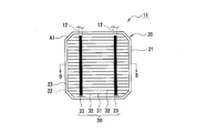
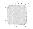
- FIGS. 2 is a diagram of the photoelectric conversion device 11 as viewed from the light receiving surface side
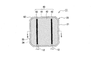
- FIG. 3 is a diagram of the photoelectric conversion device 11 as viewed from the back surface side
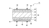
- FIG. 4 is a cross-sectional view (texture structure is omitted) taken along the line BB in FIGS. 2 and 3.
- the photoelectric conversion device 11 includes a photoelectric conversion unit 20, a light receiving surface electrode 30, and a back surface electrode 40.
- the photoelectric conversion unit 20 includes, for example, an n-type single crystal silicon substrate 21 that is a substantially square crystalline semiconductor substrate.
- the light receiving surface electrode 30 includes a transparent conductive film 31, finger electrode portions 32, and bus bar electrode portions 33.
- the back electrode 40 includes a transparent conductive film 41, a metal film 42, and a protruding electrode 43.
- the wiring member 12 (indicated by a one-dot chain line) is connected to each bus bar electrode portion 33 of the light receiving surface electrode 30 and each protruding electrode 43 of the back surface electrode 40. Is done.
- the photoelectric conversion unit 20 is formed on the light-receiving surface of the n-type single crystal silicon substrate 21 with the p-type amorphous silicon film 23 laminated via the i-type amorphous silicon film 22. Is provided. As shown in FIGS. 3 and 4, the photoelectric conversion unit 20 has an n-type amorphous silicon film 25 laminated on the back surface of the n-type single crystal silicon substrate 21 via an i-type amorphous silicon film 24. Prepare. That is, the photoelectric conversion unit 20 has a structure in which amorphous semiconductor thin films are stacked on both sides of a crystalline semiconductor substrate.
- a stacked structure in which the films 25 are stacked in this order will be exemplified.
- the p-type amorphous silicon film 23 side is the light receiving surface side.
- the i-type amorphous silicon films 22 and 24 may be laminated leaving the light receiving surface and the back edge region of the n-type single crystal silicon substrate 21.
- the i-type amorphous silicon films 22 and 24 are intrinsic amorphous silicon thin films having a lower dopant concentration than that of the p-type amorphous silicon film 23 and the n-type amorphous silicon film 25.
- the i-type amorphous silicon films 22 and 24 have the same composition, for example.
- the light-receiving surface and the back surface of the n-type single crystal silicon substrate 21 each have a texture structure.
- the “texture structure” is an uneven structure that suppresses surface reflection and increases the light absorption amount of the photoelectric conversion unit 20.
- the thickness of the photoelectric conversion portion 20 (the length in the film stacking direction) is several hundred ⁇ m, and most of the thickness is the thickness of the n-type single crystal silicon substrate 21. Among them, the uneven height of the texture structure is several ⁇ m.
- the thickness of the amorphous silicon film is several nm to several tens of nm. Since the unevenness height of the texture structure is, for example, several ⁇ m, the texture structure is also reflected on the light receiving surface and the back surface of the amorphous silicon film.
- the photoelectric conversion unit 20 can be manufactured by the following method, for example. First, a clean n-type single crystal silicon substrate 21 is placed in a vacuum chamber, and an i-type amorphous silicon film 22 is stacked on the substrate by, for example, plasma CVD (chemical vapor deposition). Subsequently, a p-type amorphous silicon film 23 is stacked on the i-type amorphous silicon film 22. In the present embodiment, the surface of the n-type single crystal silicon substrate 21 on which the p-type amorphous silicon film 23 is stacked serves as a light receiving surface.
- an i-type amorphous silicon film 24 and an n-type amorphous silicon film 25 are sequentially stacked on the back surface of the n-type single crystal silicon substrate 21 by, for example, a plasma CVD method.
- silane gas (SiH 4 ) is used as a source gas.
- stacking of the n-type amorphous silicon film 25 using silane (SiH 4 ), hydrogen (H 2 ), and phosphine (PH 3 ) as source gases.
- diborane (B 2 H 6 ) is used as the source gas instead of PH 3 .
- a transparent conductive film 31 constituting the light receiving surface electrode 30 is laminated on the light receiving surface of the p-type amorphous silicon film 23. Furthermore, on the transparent conductive film 31, a finger electrode part 32 and a bus bar electrode part 33 for collecting electric power generated by the photoelectric conversion part 20 are formed. On the other hand, a transparent conductive film 41 constituting the back electrode 40 is laminated on the back surface of the n-type amorphous silicon film 25. Furthermore, a metal film 42 for collecting the electric power generated by the photoelectric conversion unit 20 is provided on the transparent conductive film 41. On the metal film 42, a protruding electrode 43 is provided as a connection portion with the wiring material 12.
- the transparent conductive film 31 is made of, for example, a metal oxide such as indium oxide (In 2 O 3 ), zinc oxide (ZnO), tin oxide (SnO 2 ), and titanium oxide (TiO 2 ) having a polycrystalline structure.
- These metal oxides contain dopants such as tin (Sn), zinc (Zn), tungsten (W), antimony (Sb), titanium (Ti), aluminum (Al), cerium (Ce), and gallium (Ga). It may be doped. The concentration of the dopant can be 0 to 20 wt%.
- the thickness of the transparent conductive film 31 is, for example, about 50 nm to 200 nm.
- the transparent conductive film 31 is preferably laminated on the entire light receiving surface of the p-type amorphous silicon film 23 except for the edge region (hereinafter referred to as the edge region A1).
- the edge region A1 where the transparent conductive film 31 is not laminated is a surface region having a width of about 1 to 2 mm from the end of the light receiving surface of the p-type amorphous silicon film 23, and is provided in an annular shape around the light receiving surface. Is preferred.
- the transparent conductive film 31 (the same applies to the transparent conductive film 41) can be laminated by sputtering, for example, using a mask that covers the edge region A1.
- the finger electrode part 32 and the bus bar electrode part 33 are electrically connected to each other, and both are formed on the transparent conductive film 31. That is, in the light receiving surface electrode 30, carriers transmitted from the p-type amorphous silicon film 23 through the transparent conductive film 31 are collected by the finger electrode portion 32 and the bus bar electrode portion 33.
- the wiring member 12 is electrically connected to the bus bar electrode portion 33.
- the finger electrode part 32 and the bus bar electrode part 33 are formed, for example, by screen-printing a conductive paste in which conductive particles such as silver (Ag) are dispersed in a binder resin in a desired pattern on the transparent conductive film 31. It is a thin line-shaped electrode part.
- each electrode portion may be formed using various sputtering methods, various vapor deposition methods, various plating methods, or the like instead of screen printing.
- the finger electrode part 32 is, for example, a band-shaped metal layer formed on the light receiving surface, and is arranged so that power can be collected evenly from the entire photoelectric conversion part 20.
- the finger electrode portions 32 are preferably arranged in parallel with each other at a predetermined interval (for example, a width of 100 ⁇ m and an interval of 2 mm).
- the bus bar electrode part 33 further collects the power collected by the finger electrode part 32.
- the bus bar electrode part 33 is, for example, a band-shaped metal layer formed on the light receiving surface, is disposed so as to intersect the finger electrode part 32, and is electrically connected to the finger electrode part 32.
- the bus bar electrode portions 33 can be arranged in parallel with each other with a predetermined interval, for example. At this time, it is preferable that the bus bar electrode portion 33 is set to have a smaller line width than the finger electrode portions 32 and has a larger line width (for example, a width of 1.5 mm, two).
- the thickness is preferably set to be thicker than the finger electrode portion 32.
- the finger electrode portion 32 has a thickness of about 30 ⁇ m to 80 ⁇ m, for example, in order to prevent an increase in resistance due to carrier concentration. Therefore, the bus bar electrode portion 33 has a thickness of, for example, 30 ⁇ m or more, and preferably has a thickness of 50 ⁇ m or more (for example, 50 ⁇ m to 100 ⁇ m).
- the shapes of the finger electrode portion 32 and the bus bar electrode portion 33 are not limited to those exemplified here, and can be formed in various shapes such as a zigzag shape, for example.
- the transparent conductive film 41 is made of ITO, ZnO, SnO 2 or the like, like the transparent conductive film 31, and functions as a light transmissive electrode portion. Further, the transparent conductive film 41 has a function of increasing reflectance by interaction with the metal film 42 and preventing direct contact between the photoelectric conversion unit 20 and the metal film 42.
- the thickness of the transparent conductive film 41 is preferably about 50 nm to 200 nm, for example, and the texture structure is also reflected on the back surface of the transparent conductive film 41.
- the transparent conductive film 41 is preferably laminated on the entire back surface area of the n-type amorphous silicon film 25 except the edge area (hereinafter referred to as edge area A2).
- the edge region A2 where the transparent conductive film 41 is not laminated is a surface region having a width of about 1 to 2 mm from the end of the back surface of the n-type amorphous silicon film 25, and is provided in an annular shape around the back surface. Is preferred.
- the metal film 42 is a thin film made of a metal material having high light reflectivity and high conductivity.
- the reflectance of the metal film 42 is preferably a material having a high reflectance with respect to light in the infrared region having a wavelength of about 800 nm to 1200 nm.
- the reflectance of the metal film 42 is preferably higher than the reflectance of the transparent conductive film 41 for at least light in the infrared region.
- the metal material constituting the metal film 42 examples include silver (Ag), aluminum (Al), titanium (Ti), rhodium (Rh), copper (Cu), gold (Au), platinum (Pt), nickel ( Examples thereof include metals such as Ni) and chromium (Cr) or alloys containing one or more thereof.
- the metal material is preferably Ag, Al, Ti, Rh, Cu, Au, or an alloy containing one or more thereof, more preferably Ag, Al, Ti, or an alloy containing one or more thereof.
- Ag or an alloy containing Ag is particularly preferable.
- the metal film 42 reflects the transmitted light that has passed through the photoelectric conversion unit 20 to the light receiving surface side, and collects carriers transmitted from the n-type amorphous silicon film 25 through the transparent conductive film 41.
- the thickness of the metal film 42 will be described in detail. It is desirable that the thickness of the metal film 42 be thick enough that light cannot be transmitted and carriers can be sufficiently collected by the protruding electrodes 43.
- the light receiving surface electrode 30 is formed with the finger electrode portion 32 and the bus bar electrode portion 33 so as to expose the transparent conductive film 31, but as shown in FIG. Is formed so as to cover substantially the entire surface of the transparent conductive film 41.
- the metal film 42 has a larger area than the light receiving surface electrode 30.
- the photoelectric conversion unit 20 is warped according to the difference in the amount of metal material between the light-receiving surface electrode 30 and the metal film 42.
- the metal film 42 is formed thinner than the light receiving surface electrode 30. Therefore, the difference in the amount of the metal material between the light receiving surface electrode 30 and the metal film 42 is reduced, and the warpage of the photoelectric conversion unit 20 is suppressed.
- the metal film 42 is preferably thin enough to reflect the texture structure on the back surface.
- the thickness of the metal film 42 is preferably about 0.1 ⁇ m to 5 ⁇ m. If the texture structure is also reflected on the back surface of the metal film 42, an effect of improving the adhesion between the metal film 42 and the protruding electrode 43 can be obtained.
- the metal film 42 is formed so as to cover substantially the entire surface of the transparent conductive film 41, the resistance does not increase even if the thickness of the metal film 20 is reduced in this way, and the photoelectric conversion efficiency, etc. Does not affect the characteristics of
- the metal film 42 may be composed of a laminate of a plurality of films made of the above metal materials.
- a laminate of an Ag film and an Al film can be exemplified, and in this case, the Ag film is preferably disposed on the transparent conductive film 41 side.
- the metal film 42 is laminated so as to cover substantially the entire surface of the transparent conductive film 41, and more preferably, is laminated so as to cover the entire surface of the transparent conductive film 41.
- “so as to cover substantially the entire surface of the transparent conductive film 41” means a state in which the transparent conductive film 41 can be regarded as substantially covering the entire surface. This includes a state in which a part of the formed metal film 42 is missing. Specifically, a state where 95% or more of the transparent conductive film 41 is covered with the metal film 42 can be exemplified.
- the metal film 42 is preferably laminated so that at least a part of the edge region of the transparent conductive film 41 does not cover the photoelectric conversion unit 20 (n-type amorphous silicon film 25) beyond the transparent conductive film 41. It is. By laminating the metal film 42 in this way, it is possible to further suppress the defect levels that can be generated by the diffusion of metal atoms into the n-type amorphous silicon film 25. More preferably, a region where the metal film 42 is not formed is provided in an annular shape over the entire periphery of the edge region of the transparent conductive film 41.
- the width of the edge region is preferably, for example, from 1 nm to 5 mm from the end of the transparent conductive film 41, and the cross-sectional observation (width is reduced) by a scanning electron microscope (SEM) or a transmission electron microscope (TEM). If it is wide, an optical microscope can be used).
- SEM scanning electron microscope
- TEM transmission electron microscope
- the metal film 42 can be laminated by sputtering using a mask that covers the edge region A2 on the n-type amorphous silicon film 25 or the edge region on the transparent conductive film 41, for example.
- the protruding electrode 43 is a protruding electrode formed on the metal film 42 so as to protrude in the thickness direction of the photoelectric conversion unit 20.
- the protruding electrode 43 is used to electrically connect the wiring member 12 when the plurality of photoelectric conversion devices 11 are modularized. Similar to the bus bar electrode portion 33, the protruding electrode 43 is formed in a protruding shape to which the wiring material 12 can be electrically connected by, for example, screen printing a conductive paste on the metal film 42 in a desired pattern.
- the protruding electrodes 43 are, for example, strip-shaped metal layers formed on the metal film 42 and can be arranged in parallel to each other with a predetermined interval. In addition, it is preferable that the protruding electrodes 43 be arranged in the same direction as the bus bar electrode portions 33 in the same number (for example, two) as the bus bar electrode portions 33. As described above, the wiring member 12 connected to the protruding electrode 43 is connected to the bus bar electrode portion 33 of the adjacent photoelectric conversion device 11. Therefore, the connection between the photoelectric conversion device 11 and the wiring member 12 is facilitated by matching the numbers and forming directions of the bus bar electrode portions 33 and the protruding electrodes 43.
- the protruding electrode 43 is formed on the metal film 42 that is laminated so as to cover substantially the entire surface of the transparent conductive film 41, the protruding electrode 43 is not limited in thickness by the finger electrode portion 32 unlike the bus bar electrode portion 33. Therefore, the thickness of the protruding electrode 43 can be made thinner than the thickness of the bus bar electrode portion 33.
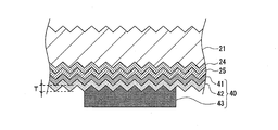
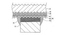
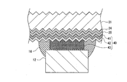
- FIG. 5 is a cross-sectional view schematically showing the protruding electrode 43 and the vicinity thereof, and is a view of the protruding electrode 43 cut in the width direction.
- FIG. 6 is a diagram illustrating a state in which the wiring member 12 is connected to the protruding electrode 43 in FIG.
- texture structures are provided on the light receiving surface and the back surface of the photoelectric conversion unit 20, respectively.
- the metal film 42 is formed thin enough to have surface irregularities corresponding to the texture structure.
- the protruding electrode 43 is formed at a height that at least fills the surface irregularities of the metal film 42 in order to enable good electrical contact with the wiring material 12. This can be realized by forming the protruding electrode 43 with a thickness equal to or higher than the surface unevenness height (T) of the metal film.
- the surface unevenness of the metal film 42 means unevenness in the thickness direction formed on the metal film 42.
- the surface unevenness height (T) means the length along the thickness direction from the bottom of the concave portion to the top of the convex portion.
- the surface irregularities are formed due to the texture structure of the n-type single crystal silicon substrate 21.
- the surface unevenness of the metal film due to the texture structure has a surface unevenness height (T) of 1 to 10 ⁇ m, for example, and is continuously formed on the entire back surface of the metal film.
- the thickness of the protruding electrode 43 is preferably not less than the average value of the surface unevenness height (T) at the electrode forming position, and more preferably not less than the maximum value of T.
- the surface roughness T caused by the texture structure is substantially uniform (average value ⁇ maximum value), for example, about 5 ⁇ m.
- the protruding electrode 43 is preferably thin so that the wiring material 12 can be sufficiently adhered onto the metal film 42 by the adhesive 16.
- the thickness of the protruding electrode 43 is preferably 1.0 to 3.0 times T, more preferably 1.1 to 2.5 times T, or 1.2 to 2.0 times T. Double is particularly preferred.
- the thickness of the protruding electrode 43 is preferably 20 ⁇ m or less, more preferably 15 ⁇ m or less, and particularly preferably 10 ⁇ m or less.
- the width of the protruding electrode 43 is not particularly limited, and may be equal to the width of the bus bar electrode portion 33 or the width of the wiring member 12, for example.
- the width of the protruding electrode 43 is, for example, about 0.5 mm to 2 mm, and may be equal to or less than the width of the wiring member 12 (for example, 0.5 mm to 1 mm).
- the thickness and width of the protruding electrode 43 can be confirmed using, for example, an optical microscope or a contact-type film thickness meter. Moreover, you may confirm by the cross-sectional observation by SEM.
- the wiring member 12 is electrically connected to the protruding electrode 43 of the back electrode 40 using an adhesive 16.
- the thin film layer of the adhesive 16 interposed between the wiring member 12 and the protruding electrode 43 is, for example, about several nanometers to several hundred nanometers (for example, it can be confirmed by cross-sectional observation by SEM or TEM).
- the wiring member 12 having a square cross section is connected to the protruding electrode 43 through the thin film layer of the adhesive 16. The connection is formed, for example, by pressing the wiring member 12 onto the protruding electrode 43 coated with the adhesive 16 and pressing it.
- a part of the adhesive 16 is pushed out from between the wiring member 12 and the protruding electrode 43 and adheres to the side surface of the protruding electrode 42 and the side surface of the wiring member 12 to cover at least a part of each side surface.
- the “side surface” of the protruding electrode 42 and the wiring member 12 means a surface along the thickness direction of each part.
- the adhesive 16 for example, a thermosetting adhesive such as an epoxy resin, or a two-component curable adhesive obtained by mixing a curing agent with an epoxy resin, an acrylic resin, a urethane resin, or the like can be used.
- the adhesive 16 may contain conductive particles.
- the adhesive 16 that does not include conductive particles for example, the wiring material 12 on which a flexible surface conductive layer such as tin (Sn) is formed is used, and a part of the protruding electrode 43 is formed on the surface conductive layer. It can also be connected by inserting.
- the width of the wiring member 12 and the width of the protruding electrode 43 are substantially equal, and are connected so that both ends in the width direction are substantially coincident.
- the protruding electrode 43 has a shape extending linearly, and the wiring member 12 is connected over the entire length of the protruding electrode 43, for example.
- the wiring member 12 has a shape extending linearly in the same manner as the protruding electrode 43 in the portion connected to the protruding electrode 43.
- the wiring member 12 is directly bonded to the metal film 42 at least at a part around the protruding electrode 43 by the adhesive 16.
- a part of the adhesive 16 protrudes from between the protruding electrode 43 and the wiring member 12, and the protruding adhesive 16 adheres onto the metal film 42 at least at a part around the protruding electrode 43.
- the protruding adhesive 16 adheres to the side surface of the protruding electrode 42 and the side surface of the wiring member 12 and covers at least a part of each side surface. Further, the protruding adhesive 16 covers, for example, the entire side surface of the protruding electrode 42 and reaches the metal film 42.
- the adhesive 16 is cured while being connected from the side surface of the wiring member 12 to the metal film 42.
- the wiring member 12 is connected to the protruding electrode 43 through the adhesive 16, and at least part of the periphery of the protruding electrode 43 on the metal film 42 due to the protruding adhesive 16. Directly glued on top.
- This connection form is easily formed by reducing the thickness of the protruding electrode 43 interposed between the wiring member 12 and the metal film 42. Further, as the thickness of the protruding electrode 43 is reduced, the coverage area of the side surface of the wiring member 12 by the adhesive 16 is increased. For example, by setting the thickness of the protruding electrode 43 to 20 ⁇ m or less, the adhesive 16 can be cured while being connected from the side surface of the wiring material 12 to the metal film 42 without using the adhesive 16 excessively. .
- the wiring member 12 is preferably directly bonded on the metal film 42 by the adhesive 16 on at least one side in the width direction of the protruding electrode 43 and directly bonded on the metal film 42 on both sides in the width direction of the protruding electrode 43. More preferably.
- the adhesive 16 is preferably attached to at least the side surface of the wiring member 12 on one side in the width direction. More preferably, the adhesive 16 adheres to the side surfaces on both sides in the width direction of the wiring material 12 to cover at least a part of the side surfaces, and the side surface of the wiring material 12 and the metal film 42 are directly bonded by the adhesive 16.
- the wiring member 12 is directly bonded onto the metal film 42 with the adhesive 16 over the entire length of the protruding electrode 43 in the longitudinal direction. Further, the wiring member 12 and the metal film 42 may be directly bonded by the adhesive 16 on both sides in the longitudinal direction of the protruding electrode 43 on the metal film 42.
- the wiring member 12 is connected to the protruding electrode 43 in a state where the width of the wiring member 12 is wider than the protruding electrode 43 and the wiring member 12 protrudes from both sides of the protruding electrode 43 in the width direction. Also good.
- This connection form can be formed, for example, by reducing the width of the protruding electrode 43 while maintaining the width of the wiring member 12. According to this connection mode, the bonding area between the wiring member 12 and the metal film 42 can be increased on both sides in the width direction of the protruding electrodes 43 on the metal film 42. Also in this case, it is preferable that the adhesive 16 covers at least a part of the side surfaces on both sides in the width direction of the wiring member 12, and the side surface of the wiring member 12 and the metal film 42 are directly bonded by the adhesive 16.
- the protruding electrodes 43 may be arranged in a plurality of rows at intervals.
- the plurality of protruding electrodes 43 are formed linearly.
- the wiring member 12 is directly bonded onto the metal film 42 by the adhesive 16 in the gap between the adjacent protruding electrodes 43.
- the formation density of the protruding electrodes 43 is not constant, and it is preferable that the density of the protruding electrodes located at the end portions of the wiring member 12 is larger than the density of the central portion.
- the adhesive force is increased at the end portion of the wiring member 12, and the photoelectric conversion device 11 is connected to the wiring member. It can suppress that 12 remove
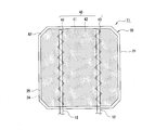
- the protruding electrode 43 may be formed in a zigzag pattern.
- the protruding electrode 43 has a shape in which sawtooth irregularities are regularly repeated over the entire length thereof, but the zigzag pattern is not limited to this. It is preferable that the wiring member 12 is directly bonded onto the metal film 42 with the adhesive 16 at least at a part around the protruding electrode 43, for example, between repeated uneven patterns.
- the metal film 42 is laminated in a wide range on the back side of the photoelectric conversion unit 20 (n-type amorphous silicon film 25). Thereby, the transmitted light that has entered from the light receiving surface and passed through the photoelectric conversion unit 20 can be reflected by the metal film 42 toward the light receiving surface.
- the metal film 42 is laminated with the photoelectric conversion unit 20 via the transparent conductive film 41, so that, for example, light absorption due to generation of evanescent light is suppressed, and the reflectance is increased. Therefore, the utilization factor of light in the photoelectric conversion unit 20 is increased, and the photoelectric conversion efficiency is improved.
- the transparent conductive film 41 can suppress the diffusion of metal atoms constituting the metal film 42 into the photoelectric conversion unit 20, and can suppress the occurrence of a defect order for trapping carriers.
- the metal film 42 is formed thinner than the light receiving surface electrode 30.
- the metal film 42 is formed thin so as to include surface irregularities reflecting the texture structure. Thereby, the difference in the amount of the metal material between the light receiving surface electrode 30 and the metal film 42 is reduced, and the warpage of the photoelectric conversion unit 20 is suppressed. Therefore, the thickness of the protruding electrode 43 can be reduced. Further, since the protruding electrode 43 is formed on the metal film 42, the thickness is not limited by the finger electrode portion 32 unlike the bus bar electrode portion 33. The thickness (T) or more can be less than the thickness of the light receiving surface electrode 20.
- the adhesive 16 covers the side surface of the protruding electrode 42 and the side surface of the wiring member 12, and the thickness of the protruding electrode 43. Over the metal film 42. That is, the adhesive 16 is connected from the side surface of the wiring material 12 to the metal film 42, and the wiring material 12 is directly bonded onto the metal film 42 by the adhesive 16. Therefore, the adhesion area between the back electrode 40 and the wiring member 12 is increased. Thereby, it is possible to suppress the wiring material 12 from being peeled off from the back electrode 40 and to improve the reliability of the photoelectric conversion module 10.
- the wiring member 12 is directly bonded onto the metal film 42 with the adhesive 16, movement of the wiring member 12 in the width direction, thickness direction (depth direction), and longitudinal direction can be suppressed. That is, the strength of the wiring material 12 in the moving direction (hereinafter referred to as a breaking force) increases.
- the wiring member 12 is directly bonded onto the metal film 42 by the adhesive 16 on both sides in the width direction of the protruding electrode 43 over the entire length thereof, so that the breaking force in the width direction and the thickness direction of the wiring member 12 is reduced. To increase.
- the wiring member 12 is directly bonded onto the metal film 42 by the adhesive 16 over the entire periphery of the protruding electrode 43, the wire breaking force in the width direction, the thickness direction, and the longitudinal direction of the wiring member 12 is reduced. To increase.
- the photoelectric conversion unit 20 having a structure in which amorphous silicon thin films are laminated on both surfaces of the n-type single crystal silicon substrate 21 is illustrated, but the structure of the photoelectric conversion unit is not limited to this.
- the photoelectric conversion unit may have a structure without the i-type amorphous silicon film 24 and the n-type amorphous silicon film 25 or a structure using a semiconductor other than silicon (for example, gallium arsenide).
- the p-type amorphous silicon film 23 side is described as the light-receiving surface side.
- the light-receiving surface electrode 30 is provided on the n-type amorphous silicon film 25 to provide an n-type amorphous silicon film.
- the 25 side may be the light receiving surface side.
- the bus bar electrode portion 33 may have various shapes in the same manner as the protruding electrode 43.
Landscapes
- Photovoltaic Devices (AREA)
- Life Sciences & Earth Sciences (AREA)
- Engineering & Computer Science (AREA)
- Sustainable Development (AREA)
- Sustainable Energy (AREA)
Abstract
Description
また、本発明に係る光電変換モジュールによれば、改善された光電変換効率を有し、信頼性の高い光電変換モジュールを提供することができる。
以下の実施形態は、単なる例示である。本発明は、以下の実施形態に限定されない。また、実施形態において参照する図面は、模式的に記載されたものであり、図面に描画された物体の寸法比率などは、現実の物体の寸法比率などとは異なる場合がある。具体的な物体の寸法比率等は、以下の説明を参酌して判断されるべきである。
光電変換モジュール10は、複数の光電変換装置11と、各光電変換装置11を電気的に接続する配線材12とを備える。また、光電変換モジュール10は、光電変換装置11の受光面側を保護する第1保護部材13と、光電変換装置11の裏面側を保護する第2保護部材14とを備えることが好適である。そして、第1保護部材13と第2保護部材14との間には、封止材15が充填される。光電変換装置11と配線材12とは、接着剤16(後述の図6に参照)を用いて接続できる。
図2は、光電変換装置11を受光面側から見た図であり、図3は、光電変換装置11を裏面側から見た図である。図4は、図2及び図3のB‐B線に沿った断面図(テクスチャ構造は省略)を示す。
Claims (18)
- 受光面及び裏面にテクスチャ構造が形成された光電変換部と、
前記光電変換部の受光面に設けられた受光面電極と、
前記光電変換部の裏面に設けられた裏面電極と、
を備え、
前記裏面電極は、
前記光電変換部の裏面に積層された透明導電膜と、
前記透明導電膜上の略全面に積層され、前記テクスチャ構造を反映した表面凹凸を有する金属膜と、
前記金属膜上に形成され、該金属膜の表面凹凸高さ以上の厚みを有する突起電極と、
を含む光電変換装置。 - 請求項1に記載の光電変換装置であって、
前記突起電極は、受光面電極の厚みよりも薄く形成された光電変換装置。 - 請求項1又は2に記載の光電変換装置であって、
前記金属膜は、前記透明導電膜上の全面に積層された光電変換装置。 - 請求項1~3のいずれか1に記載の光電変換装置であって、
前記金属膜の反射率は、少なくとも波長800nm~1200nmの赤外領域の光について、前記透明導電膜の反射率よりも高い光電変換装置。 - 請求項1~3のいずれか1に記載の光電変換装置であって、
前記金属膜は、少なくともAgを含む膜である光電変換装置。 - 請求項1~5のいずれか1に記載の光電変換装置であって、
前記光電変換部は、
結晶系半導体基板と、
前記結晶系半導体基板の裏面に積層された非晶質半導体膜と、
を含み、
前記透明導電膜は、前記非晶質半導体膜の裏面に積層されている光電変換装置。 - 光電変換装置と、
前記光電変換装置に電気的に接続された配線材と、
を備え、
前記光電変換装置は、
光電変換部と、
前記光電変換部の受光面に設けられた受光面電極と、
前記光電変換部の裏面に積層された透明導電膜、前記透明導電膜上の略全面に積層された金属膜、及び前記金属膜上に形成された突起電極を有する裏面電極と、
を含み、
前記配線材は、
接着剤を介して前記突起電極に電気的に接続され、前記金属膜上の前記突起電極の周囲の少なくとも一部において前記接着剤により前記金属膜上に直接接着されている光電変換モジュール。 - 請求項7に記載の光電変換モジュールにおいて、
前記配線材は、その側面に前記接着剤が付着しており、該側面と前記金属膜とが前記接着剤により直接接着されている光電変換モジュール。 - 請求項7又は8に記載の光電変換モジュールであって、
前記金属膜は、前記透明導電膜上の全面に積層された光電変換モジュール。 - 請求項7~9のいずれか1に記載の光電変換モジュールであって、
前記光電変換部の前記受光面及び前記裏面には、テクスチャ構造が形成されると共に、前記金属膜は、該テクスチャ構造を反映した表面凹凸を含むように薄く形成され、
前記突起電極の厚みは、前記金属膜の表面凹凸高さ以上受光面電極の厚み未満である光電変換モジュール。 - 請求項7~10のいずれか1に記載の光電変換モジュールであって、
前記配線材は、少なくとも前記金属膜上の前記突起電極の幅方向片側において、前記接着剤により前記金属膜上に直接接着されている光電変換モジュール。 - 請求項11に記載の光電変換モジュールであって、
前記配線材は、前記金属膜上の前記突起電極の幅方向両側において、前記接着剤により前記金属膜上に直接接着されている光電変換モジュール。 - 請求項11又は12に記載の光電変換モジュールであって、
前記配線材は、前記突起電極よりも幅広であり、少なくとも該突起電極の幅方向片側から張り出した状態で互いに接続されている光電変換モジュール。 - 請求項7~10のいずれか1に記載の光電変換モジュールであって、
前記配線材は、前記金属膜上の前記突起電極の全周囲に亘って、前記接着剤により前記金属膜上に直接接着されている光電変換モジュール。 - 請求項7~10のいずれか1に記載の光電変換モジュールであって、
複数の前記突起電極が、互いに間隔をあけて列状に並んで配置され、
前記配線材は、隣り合う前記突起電極の間隙において、前記接着剤により前記金属膜上に直接接着されている光電変換モジュール。 - 請求項7~15のいずれか1に記載の光電変換モジュールであって、
前記金属膜の反射率は、少なくとも波長800nm~1200nmの赤外領域の光について、前記透明導電膜の反射率よりも高い光電変換モジュール。 - 請求項7~16のいずれか1に記載の光電変換モジュールであって、
前記金属膜は、少なくともAgを含む膜である光電変換モジュール。 - 請求項7~17のいずれか1に記載の光電変換モジュールであって、
前記光電変換部は、
結晶系半導体基板と、
前記結晶系半導体基板の裏面に積層された非晶質半導体膜と、
を含み、
前記透明導電膜は、前記非晶質半導体膜の裏面に積層されている光電変換モジュール。
Priority Applications (3)
| Application Number | Priority Date | Filing Date | Title |
|---|---|---|---|
| EP20110857750 EP2657981A4 (en) | 2011-01-31 | 2011-12-27 | PHOTOELECTRIC TRANSFORMER AND PHOTOELECTRIC CONVERSION MODULE |
| JP2012555705A JPWO2012105146A1 (ja) | 2011-01-31 | 2011-12-27 | 光電変換装置及び光電変換モジュール |
| US13/954,549 US20130312826A1 (en) | 2011-01-31 | 2013-07-30 | Photovoltaic device and photovoltaic module |
Applications Claiming Priority (2)
| Application Number | Priority Date | Filing Date | Title |
|---|---|---|---|
| JP2011018381 | 2011-01-31 | ||
| JP2011-018381 | 2011-01-31 |
Related Child Applications (1)
| Application Number | Title | Priority Date | Filing Date |
|---|---|---|---|
| US13/954,549 Continuation US20130312826A1 (en) | 2011-01-31 | 2013-07-30 | Photovoltaic device and photovoltaic module |
Publications (1)
| Publication Number | Publication Date |
|---|---|
| WO2012105146A1 true WO2012105146A1 (ja) | 2012-08-09 |
Family
ID=46602376
Family Applications (1)
| Application Number | Title | Priority Date | Filing Date |
|---|---|---|---|
| PCT/JP2011/080165 Ceased WO2012105146A1 (ja) | 2011-01-31 | 2011-12-27 | 光電変換装置及び光電変換モジュール |
Country Status (4)
| Country | Link |
|---|---|
| US (1) | US20130312826A1 (ja) |
| EP (1) | EP2657981A4 (ja) |
| JP (1) | JPWO2012105146A1 (ja) |
| WO (1) | WO2012105146A1 (ja) |
Cited By (4)
| Publication number | Priority date | Publication date | Assignee | Title |
|---|---|---|---|---|
| EP2849233A1 (en) | 2013-09-17 | 2015-03-18 | Sanyo Electric Co., Ltd | Solar cell |
| JPWO2014132287A1 (ja) * | 2013-02-27 | 2017-02-02 | パナソニックIpマネジメント株式会社 | 太陽電池モジュール及び太陽電池モジュールの製造方法 |
| JPWO2014192272A1 (ja) * | 2013-05-28 | 2017-02-23 | パナソニックIpマネジメント株式会社 | 太陽電池モジュール |
| JPWO2015194147A1 (ja) * | 2014-06-18 | 2017-04-20 | パナソニックIpマネジメント株式会社 | 太陽電池モジュール |
Families Citing this family (4)
| Publication number | Priority date | Publication date | Assignee | Title |
|---|---|---|---|---|
| KR20150045309A (ko) * | 2013-10-18 | 2015-04-28 | 엘지이노텍 주식회사 | 태양전지 모듈 |
| WO2016052635A1 (ja) * | 2014-09-30 | 2016-04-07 | 株式会社カネカ | 結晶シリコン系太陽電池の製造方法、及び太陽電池モジュールの製造方法 |
| CN107534068B (zh) * | 2015-01-06 | 2020-08-04 | 协鑫集成科技(香港)有限公司 | 用于光伏模块生产的纹理化带 |
| EP4300597A3 (en) * | 2015-10-08 | 2024-03-27 | Shangrao Xinyuan YueDong Technology Development Co. Ltd | Solar cell module |
Citations (4)
| Publication number | Priority date | Publication date | Assignee | Title |
|---|---|---|---|---|
| JPH08508368A (ja) * | 1993-10-11 | 1996-09-03 | ユニヴェルシテ ドゥ ヌーシャテル アンスティチュ ドゥ ミクロテクニク | 光電池および光電池を製造するための方法 |
| JP2009290234A (ja) | 2009-09-07 | 2009-12-10 | Sanyo Electric Co Ltd | 光起電力素子 |
| JP2010238938A (ja) * | 2009-03-31 | 2010-10-21 | Sanyo Electric Co Ltd | 太陽電池セル、太陽電池モジュールおよび太陽電池システム |
| JP2011003750A (ja) * | 2009-06-19 | 2011-01-06 | Kaneka Corp | 結晶シリコン系太陽電池 |
Family Cites Families (8)
| Publication number | Priority date | Publication date | Assignee | Title |
|---|---|---|---|---|
| JP2002141534A (ja) * | 2000-11-02 | 2002-05-17 | Sharp Corp | 半導体基板の電極及びその製造方法 |
| WO2005109524A1 (ja) * | 2004-05-07 | 2005-11-17 | Mitsubishi Denki Kabushiki Kaisha | 太陽電池及びその製造方法 |
| JP2006278710A (ja) * | 2005-03-29 | 2006-10-12 | Kyocera Corp | 太陽電池モジュール及びその製造方法 |
| JP4294048B2 (ja) * | 2006-11-29 | 2009-07-08 | 三洋電機株式会社 | 太陽電池モジュール |
| JP4463297B2 (ja) * | 2007-08-07 | 2010-05-19 | 三洋電機株式会社 | 太陽電池モジュール |
| US20100224228A1 (en) * | 2009-03-03 | 2010-09-09 | Jinah Kim | Solar cell and method for manufacturing the same, and solar cell module |
| JP5515367B2 (ja) * | 2009-03-31 | 2014-06-11 | 三洋電機株式会社 | 太陽電池セル、太陽電池モジュールおよび太陽電池システム |
| EP2426726A1 (en) * | 2009-04-30 | 2012-03-07 | Mitsubishi Electric Corporation | Solar battery cell |
-
2011
- 2011-12-27 JP JP2012555705A patent/JPWO2012105146A1/ja active Pending
- 2011-12-27 EP EP20110857750 patent/EP2657981A4/en not_active Withdrawn
- 2011-12-27 WO PCT/JP2011/080165 patent/WO2012105146A1/ja not_active Ceased
-
2013
- 2013-07-30 US US13/954,549 patent/US20130312826A1/en not_active Abandoned
Patent Citations (4)
| Publication number | Priority date | Publication date | Assignee | Title |
|---|---|---|---|---|
| JPH08508368A (ja) * | 1993-10-11 | 1996-09-03 | ユニヴェルシテ ドゥ ヌーシャテル アンスティチュ ドゥ ミクロテクニク | 光電池および光電池を製造するための方法 |
| JP2010238938A (ja) * | 2009-03-31 | 2010-10-21 | Sanyo Electric Co Ltd | 太陽電池セル、太陽電池モジュールおよび太陽電池システム |
| JP2011003750A (ja) * | 2009-06-19 | 2011-01-06 | Kaneka Corp | 結晶シリコン系太陽電池 |
| JP2009290234A (ja) | 2009-09-07 | 2009-12-10 | Sanyo Electric Co Ltd | 光起電力素子 |
Non-Patent Citations (1)
| Title |
|---|
| See also references of EP2657981A4 |
Cited By (4)
| Publication number | Priority date | Publication date | Assignee | Title |
|---|---|---|---|---|
| JPWO2014132287A1 (ja) * | 2013-02-27 | 2017-02-02 | パナソニックIpマネジメント株式会社 | 太陽電池モジュール及び太陽電池モジュールの製造方法 |
| JPWO2014192272A1 (ja) * | 2013-05-28 | 2017-02-23 | パナソニックIpマネジメント株式会社 | 太陽電池モジュール |
| EP2849233A1 (en) | 2013-09-17 | 2015-03-18 | Sanyo Electric Co., Ltd | Solar cell |
| JPWO2015194147A1 (ja) * | 2014-06-18 | 2017-04-20 | パナソニックIpマネジメント株式会社 | 太陽電池モジュール |
Also Published As
| Publication number | Publication date |
|---|---|
| EP2657981A4 (en) | 2014-02-26 |
| US20130312826A1 (en) | 2013-11-28 |
| JPWO2012105146A1 (ja) | 2014-07-03 |
| EP2657981A1 (en) | 2013-10-30 |
Similar Documents
| Publication | Publication Date | Title |
|---|---|---|
| US20140130857A1 (en) | Photoelectric converter and method for producing same | |
| JP5687506B2 (ja) | 太陽電池及び太陽電池モジュール | |
| JPWO2012105146A1 (ja) | 光電変換装置及び光電変換モジュール | |
| JP5874011B2 (ja) | 太陽電池及び太陽電池モジュール | |
| WO2019146366A1 (ja) | 太陽電池モジュール | |
| US9425340B2 (en) | Solar cell and solar cell module | |
| JP6677801B2 (ja) | 結晶シリコン系太陽電池およびその製造方法、ならびに太陽電池モジュール | |
| US20120048374A1 (en) | Thin film solar cell and manufacturing method thereof | |
| CN112640134A (zh) | 太阳能电池模块 | |
| JP5554409B2 (ja) | 光電変換装置 | |
| JP7270607B2 (ja) | 太陽電池セルの製造方法、太陽電池モジュールの製造方法、および、太陽電池モジュール | |
| WO2013001861A1 (ja) | 太陽電池及びその製造方法 | |
| JP2016086154A (ja) | 太陽電池モジュール | |
| JP2010287715A (ja) | 薄膜太陽電池およびその製造方法 | |
| WO2013014972A1 (ja) | 光起電力モジュール | |
| CN110870081A (zh) | 太阳能电池以及太阳能电池模块 | |
| JP2011124474A (ja) | 多接合型太陽電池、該多接合型太陽電池を備えた太陽電池モジュール、及び該多接合型太陽電池の製造方法 | |
| JPH11298020A (ja) | 薄膜太陽電池モジュール | |
| US20190305151A1 (en) | Solar cell and manufacturing method of the same | |
| WO2015045263A1 (ja) | 太陽電池及び太陽電池モジュール | |
| WO2012105153A1 (ja) | 光電変換素子 | |
| WO2013046338A1 (ja) | 太陽電池及び太陽電池モジュール |
Legal Events
| Date | Code | Title | Description |
|---|---|---|---|
| 121 | Ep: the epo has been informed by wipo that ep was designated in this application |
Ref document number: 11857750 Country of ref document: EP Kind code of ref document: A1 |
|
| ENP | Entry into the national phase |
Ref document number: 2012555705 Country of ref document: JP Kind code of ref document: A |
|
| REEP | Request for entry into the european phase |
Ref document number: 2011857750 Country of ref document: EP |
|
| WWE | Wipo information: entry into national phase |
Ref document number: 2011857750 Country of ref document: EP |
|
| NENP | Non-entry into the national phase |
Ref country code: DE |