WO2012102083A1 - 半導体集積回路 - Google Patents
半導体集積回路 Download PDFInfo
- Publication number
- WO2012102083A1 WO2012102083A1 PCT/JP2012/050433 JP2012050433W WO2012102083A1 WO 2012102083 A1 WO2012102083 A1 WO 2012102083A1 JP 2012050433 W JP2012050433 W JP 2012050433W WO 2012102083 A1 WO2012102083 A1 WO 2012102083A1
- Authority
- WO
- WIPO (PCT)
- Prior art keywords
- division ratio
- ratio setting
- setting unit
- semiconductor integrated
- integrated circuit
- Prior art date
- Legal status (The legal status is an assumption and is not a legal conclusion. Google has not performed a legal analysis and makes no representation as to the accuracy of the status listed.)
- Ceased
Links
Images





Classifications
-
- H—ELECTRICITY
- H03—ELECTRONIC CIRCUITRY
- H03L—AUTOMATIC CONTROL, STARTING, SYNCHRONISATION OR STABILISATION OF GENERATORS OF ELECTRONIC OSCILLATIONS OR PULSES
- H03L7/00—Automatic control of frequency or phase; Synchronisation
- H03L7/06—Automatic control of frequency or phase; Synchronisation using a reference signal applied to a frequency- or phase-locked loop
- H03L7/16—Indirect frequency synthesis, i.e. generating a desired one of a number of predetermined frequencies using a frequency- or phase-locked loop
- H03L7/18—Indirect frequency synthesis, i.e. generating a desired one of a number of predetermined frequencies using a frequency- or phase-locked loop using a frequency divider or counter in the loop
- H03L7/183—Indirect frequency synthesis, i.e. generating a desired one of a number of predetermined frequencies using a frequency- or phase-locked loop using a frequency divider or counter in the loop a time difference being used for locking the loop, the counter counting between fixed numbers or the frequency divider dividing by a fixed number
Definitions
- the present invention relates to a semiconductor integrated circuit incorporating a PLL (phase locked loop) used for LNB (low noise block down converter).
- PLL phase locked loop
- LNB low noise block down converter
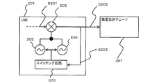
- FIG. 9 shows a satellite broadcast receiving system including a conventional LNB 201 mounted on a satellite broadcasting antenna and a satellite broadcast tuner 301 connected to the LNB 201, which is used in Patent Document 1. As shown in FIG. The configuration and operation of frequency conversion in LNB 201 will be described below.
- the LNB 201 includes a mixer 202 for converting the frequency of a broadcast signal from a satellite to a reception frequency of a satellite broadcast tuner, and local oscillators 203 and 204 for exciting the mixer 202.
- the signal S 201 of 10.7 GHz to 12.75 GHz transmitted from the satellite is frequency-converted by the mixer 202 into a signal S 202 of 950 MHz to 2150 MHz, which is the reception frequency of the satellite broadcast tuner 301.
- the LNB 201 also includes a plurality of local oscillators 203 and 204 having different oscillation frequencies.
- the local oscillators 203 and 204 respectively receive the signal S201 of 10.7 GHz to 12.75 GHz by dividing the frequency into 10.7 GHz to 11.7 GHz and 11.7 GHz to 12.75 GHz. It corresponds to the frequency band.
- the switching circuit 205 switches the plurality of local oscillators 203 and 204 in accordance with the respective frequency bands.
- the switching circuit 205 is controlled by a pulse signal S 203 on which the frequency band switching signal sent from the satellite broadcast tuner 301 is superimposed.
- LNBs have relatively high processing frequencies. Therefore, interference between circuits is likely to occur, and integration of main circuits is difficult.
- FIG. 10 shows a semiconductor integrated circuit for LNB proposed in Non-Patent Document 1, and an operation relating to frequency conversion will be described below along with the configuration.
- the PLL circuit 404 is controlled based on the multi-bit channel selection signal S403 from the external channel selection unit 406. By this control, the PLL circuit 404 varies the oscillation frequency of the local oscillator 403 by the DC voltage passed through the low-pass filter 405 provided outside.
- the signal S401 of 10.7 GHz to 12.75 GHz transmitted from the satellite is frequency-converted by the mixer 402 into the signal S402 of 950 MHz to 2150 MHz, which is the reception frequency of the satellite broadcast tuner (not shown).
- Japanese Patent Publication Japanese Patent Application Laid-Open No. 8-293812 (released on November 5, 1996).
- the local oscillators 203 and 204 use frequencies of 9.75 GHz and 10.6 GHz, respectively. As frequencies other than these frequencies, for example, 10.678 GHz for BS for Japan and 110 ° CS broadcasting and 10.7 GHz for CS broadcasting, local oscillators can not be shared between Europe and Japan .
- the LNB and the satellite broadcast receiver are connected by one coaxial cable. Then, it is possible to incorporate a large-scale control bus because it switches 9.75 GHz and 10.6 GHz depending on whether or not a pulse signal on which the frequency band switching signal is superimposed is applied to the LNB via this coaxial cable. Absent.
- the above frequency is the frequency only in the region called universal in Europe, it is necessary to set fixedly at the manufacturing stage at 10.678 GHz, which is the local oscillation frequency of other products such as for Japan. There is. Therefore, when the frequency setting for each destination is not set at the manufacturing stage, the local oscillation frequency setting of the LNB is performed by the user when constructing the reception environment such as installation of the satellite broadcasting antenna, and the convenience is lost. May be
- the present invention provides a simple and low-cost semiconductor integrated circuit for LNB that can obtain a local oscillation signal corresponding to satellite broadcasting of each country.
- the present invention comprises a local oscillator capable of oscillating operation at a plurality of frequencies, a reference signal oscillator oscillating at a predetermined reference frequency, and a variable frequency divider dividing an output signal of the local oscillator by n times the reference frequency , And the first division ratio setting unit that controls the division ratio of the variable divider according to the supplied DC potential, and the presence or absence of the supplied pulse signal. And a second division ratio setting unit for controlling the division ratio of the variable divider, wherein the variable division is performed by the first division ratio setting unit or the second division ratio setting unit.
- the oscillation frequency of the local oscillator is set to a desired frequency by control of division ratio of the oscillator.
- the semiconductor integrated circuit according to the present invention is characterized in that the direct current potential is supplied to the first division ratio setting unit via a current mirror circuit.
- FIG. 10 is a block diagram showing a modified example 1 of the first embodiment.
- FIG. 10 is a block diagram showing a modified example 2 of the first embodiment.
- FIG. 16 is a block diagram showing a modification 3 of the first embodiment. It is a block diagram which shows the semiconductor integrated circuit which concerns on Example 2 of this invention.
- FIG. 13 is a block diagram showing a modification of the second embodiment. It is a block diagram showing a semiconductor integrated circuit concerning Example 3 of the present invention. It is a block diagram which shows the semiconductor integrated circuit which concerns on Example 4 of this invention. It is a block diagram which shows the conventional LNB. It is a block diagram showing the conventional semiconductor integrated circuit.
- FIG. 2 is a block diagram showing a division ratio setting unit according to a first embodiment.
- FIG. 16 is a block diagram showing a division ratio setting unit according to a fourth embodiment.
- Example 1 First Embodiment A semiconductor integrated circuit according to a first embodiment of the present invention will be described with reference to FIGS.
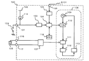
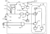
- FIG. 1 is a block diagram of a semiconductor integrated circuit 100 according to a first embodiment
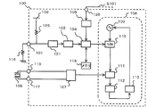
- FIGS. 2 to 4 are block diagrams showing each of the first to third modifications of the first embodiment.
- the semiconductor integrated circuit 100 includes a division ratio setting voltage terminal 101, an AD converter 103, a division ratio setting unit 104, a detector 105, a PLL circuit 108, and a memory 118. Further, a first division ratio setting unit is configured by the AD converter 103, the division ratio setting unit 104, and the memory 118, and a second division ratio setting is performed by the detector 105, the division ratio setting unit 104, and the memory 118. Make up the department.
- the PLL circuit 108 includes a local oscillator 109, a variable frequency divider 110, a phase comparator 111, a charge pump 112, and a loop filter 113. As in the prior art document, the local oscillator 109 is connected to a mixer (not shown).
- the local oscillator 109 is a local oscillator that can oscillate and operate at a plurality of oscillation frequencies.
- the variable frequency divider 110 divides the output signal of the local oscillator 109 by n times the reference frequency described later.
- the semiconductor integrated circuit 100 can obtain the desired local oscillation frequency in two ways, one using the first division ratio setting unit and the other using the second division ratio setting unit. Explain to.
- division ratio setting voltage terminal 101 When the first division ratio setting unit is used, division ratio setting voltage terminal 101 is connected to power supply 102 via current source 114, and between division ratio setting voltage terminal 101 and the ground potential. A resistor 115 is connected to. One end of the resistor 115 is connected to the input of the AD converter 103, and the other end is electrically grounded. Also, the present invention is not limited to this.
- the division ratio setting voltage terminal 101 may be connected to the power supply 102 (ie, the voltage source 102) without the current source 114, or connected to the ground potential without the resistor 115. I don't care.
- the resistor 115 in FIG. 1 may be replaced with the variable resistor 123, or may be replaced with the switch 124 as shown in the second modification of FIG.
- the power supply 102 and the division ratio setting voltage terminal 101 may be connected by the resistor 125.
- a voltage corresponding to the resistance value between the reference voltage (i.e., the ground potential) and the reference voltage (i.e., the ground voltage) is generated at the division ratio setting voltage terminal 101 which is the supply end of the DC voltage.
- the voltage generated at the division ratio setting voltage terminal 101 is converted to a binarized signal (binarized signal) after being input to the AD converter 103.
- This binarized signal is input to the division ratio setter 104.
- the division ratio setting unit 104 generates a division ratio control signal that controls the division ratio of the variable divider 110.
- the division ratio setting unit 104 collates the signal binarized by the AD converter 103 with the division ratio setting data stored in the memory 118. As a result of comparison, division ratio setting data corresponding to the binarized signal is selected, and a division ratio control signal corresponding to the desired division ratio is transmitted to the variable divider 110.
- a pulse signal S101 from a satellite broadcast tuner (not shown) is applied to the terminal 126, and the detector 105 detects this pulse signal S101, and a detection output signal corresponding to the presence or absence of the pulse signal S101 is a division ratio setter 104.
- the satellite broadcast tuner is, for example, a tuner provided outside the semiconductor integrated circuit 100.
- the division ratio setting unit 104 collates the detection output signal from the detector 105 with the division ratio setting data stored in the memory 118, and changes the division ratio control signal corresponding to the presence or absence of the pulse signal S101. It transmits to the frequency divider 110.
- the division ratio setting by the second division ratio setting unit is performed, the voltage of the division ratio setting voltage terminal 101 and the division ratio by the first division ratio setting unit stored in the memory 118 are used. Associate setting data that makes settings invalid. By doing this, the division ratio setting by the second division ratio setting unit may be selected.
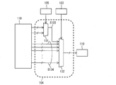
- Division ratio setter 104 is configured as shown in FIG. 11 and includes multiplexers 131 and 132 for collating with a plurality of division ratio setting data stored in memory 118.
- the multiplexer 131 selects the division ratio control signal S133 determined by the detection output signal from the detector 105, and the multiplexer 132 selects the division ratio control signal S133 and the division ratio control signal S134 which does not depend on the detection output signal. Are selected by the binarized signal output from the AD converter 103.
- division ratio setting data is selected, and a division ratio control signal corresponding to a desired division ratio is transmitted to variable divider 110.
- variable frequency divider 110 divides the frequency division ratio based on the division ratio control signal obtained by either the first or second division ratio setting.
- the output signal is transmitted to the phase comparator 111.
- the phase comparator 111 uses the output signal of the variable frequency divider 110 and the reference signal oscillator 107 that generates a predetermined reference frequency using the crystal oscillator 106 externally connected via the terminals 116 and 117. Compare the differences. Then, an output signal indicating the comparison result is transmitted to the charge pump 112.
- the charge pump 112 generates a current according to the output signal of the phase comparator.
- Loop filter 113 converts the signal from charge pump 112 into a control voltage of local oscillator 109.
- the local oscillator 109 oscillates at an oscillation frequency corresponding to the control voltage from the charge pump 112, whereby a desired local oscillation frequency can be obtained.
- the above is the series of operations for obtaining the desired local oscillation frequency in the semiconductor integrated circuit 100.
- the case of division ratio setting by the first division ratio setting unit is considered.
- the division ratio of the variable divider 110 is determined in advance by what multiple of the reference frequency. The relationship between the reference frequency and the division ratio will be described below.
- an oscillation frequency of 9.75 GHz is obtained by setting the division ratio of the variable divider 110 to 390 times by the division ratio control signal of the division ratio setter 104.
- an oscillation frequency of 10.6 GHz can be obtained by setting the dividing ratio of the variable divider 110 to 424 times by the dividing ratio control signal of the dividing ratio setter 104.
- division ratio setting 10.7 GHz can be obtained by setting the division ratio of the variable divider 110 to 428 times by the division ratio control signal of the unit 104.
- 10.75 GHz can be obtained by setting the dividing ratio of the variable divider 110 to 430 times by the dividing ratio control signal of the dividing ratio setter 104 with respect to 25 MHz which is the reference frequency. .
- the division ratio setting is performed by the second division ratio setting unit.
- the presence / absence of pulse signal S101 from a satellite broadcast tuner (not shown) is detected by detector 105, and when pulse signal S101 is absent, the division ratio control signal corresponding to the local oscillation frequency of 9.75 GHz is divided.
- the pulse signal S101 is transmitted from the ratio setter 104 to the variable divider 110, the division ratio control signal corresponding to the local oscillation frequency of 10.6 GHz is transmitted from the division ratio setter 104 to the variable divider 110.
- the Integer-N PLL is described as an example, but it can also be used in the Fractional-N PLL.
- the division ratio control of the variable divider 110 by the terminal voltage setting of the division ratio setting voltage terminal 101 and the variable component by the pulse signal S101 transmitted from the external satellite broadcast tuner
- the division ratio of the frequency divider 110 it is possible to realize a semiconductor integrated circuit for LNB corresponding to destinations in various countries with a single circuit specification.
- Example 2 Next, a second embodiment of the semiconductor integrated circuit of the present invention will be described with reference to FIGS.
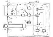
- FIG. 5 shows a block diagram of a semiconductor integrated circuit 200 according to a second embodiment
- FIG. 6 shows a modification of the semiconductor integrated circuit 200.
- the configuration and operation will be described below. 5 and 6, the same parts as those of the first embodiment are denoted by the same reference numerals, and the description of the same parts as the first embodiment will not be repeated.
- FIG. 5 is different from the first embodiment of FIG. 1 in that a potential is supplied from the current source 114 to the division ratio setting voltage terminal 101 via the current mirror circuit 119.
- a potential is supplied from the current source 114 to the division ratio setting voltage terminal 101 via the current mirror circuit 119.
- the potential of the division ratio setting voltage terminal 101 can be set as in the first embodiment.
- the voltage of the division ratio setting voltage terminal 101 can be set to the voltage of the power supply voltage by eliminating the resistor 115 in FIG.
- the power supply voltage itself can be used as the voltage of the division ratio setting voltage terminal 101 in addition to the voltage value corresponding to the resistance value between the division ratio setting voltage terminal 101 and the reference potential, so the voltage setting range is expanded.
- the division ratio setting range of the division ratio setting unit 102 can be expanded.
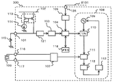
- FIG. 7 shows a block diagram of a semiconductor integrated circuit 300 according to the third embodiment.
- the same parts as those of the first and second embodiments are denoted by the same reference numerals, and the description of the same parts as the first and second embodiments will not be repeated.
- a buffer circuit 121 is provided between the division ratio setting voltage terminal 101 and the AD converter 103.
- the provision of the buffer circuit 121 has the following operational advantages.
- the voltage of the division ratio setting voltage terminal 101 falls to an unintended voltage. That is, the input voltage to the AD converter 103 is lowered, and the division ratio setting unit 104 controls the variable divider 110 with an unintended division ratio setting signal, resulting in a desired local oscillation frequency. It can not be obtained. Assuming such a case, by driving the AD converter 103 via the buffer circuit 121 with low output impedance, the AD converter 103 and the division ratio setting unit 104 can be operated stably.
- Example 4 Fourth Embodiment A semiconductor integrated circuit according to a fourth embodiment of the present invention will be described with reference to FIG.
- FIG. 8 shows a block diagram of a semiconductor integrated circuit 400 according to the fourth embodiment.
- the same parts as those in the first, second and third embodiments are denoted by the same reference numerals, and the description of the same parts as those in the first, second and third embodiments will not be repeated.
- the reference frequency control signal S102 is supplied to a switched capacitor or a band pass filter circuit which selects a pulse signal.
- the use of the reference frequency control signal S102 has the following manufacturing advantages.
- Division ratio setter 104 is configured as shown in FIG. 12 and includes multiplexers 131 and 132 for collating with a plurality of division ratio setting data stored in memory 118.
- the multiplexer 131 selects the division ratio control signal S133 determined by the detection output signal from the detector 105, and the multiplexer 132 selects the division ratio control signal S133 and the division ratio control signal S134 which does not depend on the detection output signal. Are selected by the binarized signal output from the AD converter 103.
- division ratio setting data is selected, and a division ratio control signal corresponding to a desired division ratio is transmitted to variable divider 110.
- the reference frequency control signal S102 is output to another circuit 122 when a certain division ratio control signal is output.
- the internal operation reference frequency may be shared by a plurality of circuits.
- another circuit 122 in FIG. 8 shares the reference frequency of the reference signal oscillator 107 using the crystal oscillator 106.
- the local oscillator 109 is desired.
- the oscillation frequency can be coped with by setting the division ratio of the variable frequency divider 110, but the other circuit 122 malfunctions due to the changed reference frequency.
- the local oscillation frequency of the domestic BS and 110 ° CS broadcasting is 10.678 GHz.
- the reference frequency of the reference signal oscillator 107 is 19 MHz
- a reference signal is generated by the corresponding crystal oscillator 106
- the division ratio setting unit 104 divides the division ratio of the variable divider 110 by 562 It is possible to obtain 10.678 GHz which is a desired local oscillation frequency by performing control such that
- the division ratio setting unit 104 changes the operation reference frequency of the other circuit 122 to 19 MHz by supplying the reference frequency control signal S102 to the other circuit 122 so that such a malfunction does not occur.
- Circuit 122 is set to operate at the modified reference frequency.
- the reference frequency of the reference signal oscillator 107 can be determined in accordance with the division ratio setting of the variable frequency divider 110, the degree of freedom in selecting the crystal oscillator can be improved.
- a local oscillator capable of oscillating operation at a plurality of frequencies, a reference signal oscillator oscillating at a predetermined reference frequency, and an output signal of the local oscillator are divided by n times the reference frequency
- a semiconductor integrated circuit including a variable frequency divider, wherein the first frequency division ratio setting unit controls the frequency division ratio of the variable frequency divider according to the supplied DC potential; and the supplied pulse And a second division ratio setting unit configured to control the division ratio of the variable divider according to the presence or absence of a signal, wherein the first division ratio setting unit or the second division ratio setting unit
- the oscillation frequency of the local oscillator is set to a desired frequency by the division ratio control of the variable frequency divider according to the above.
- the first division ratio setting unit is an AD converter for converting the DC potential into a binary signal, a memory storing division ratio setting data, and the binary.
- a division ratio setting unit is provided for generating a division ratio control signal of the variable divider from the division signal and the division ratio setting data.
- the second division ratio setting unit may include a detector for detecting the pulse signal, a memory storing division ratio setting data, and a detection output signal of the detector. It is characterized by comprising a division ratio setting unit that generates a division ratio control signal of the variable divider from division ratio setting data.
- the semiconductor integrated circuit according to the present invention is characterized in that the direct current potential is supplied to the first division ratio setting unit via a current mirror circuit.
- the semiconductor integrated circuit according to the present invention is characterized in that the direct current potential is supplied to the first division ratio setting unit via a buffer circuit.
- the semiconductor integrated circuit according to the present invention is characterized in that the direct current potential is a voltage corresponding to a resistance value between the supply end of the direct current potential and the ground potential.
- the semiconductor integrated circuit according to the present invention is characterized in that the division ratio setting unit supplies a reference frequency control signal to a predetermined circuit in accordance with the change of the reference frequency.
- the semiconductor integrated circuit according to the present invention can be suitably used for LNBs compatible with broadcast frequencies in countries around the world with a simple configuration. Further, the present invention can be widely applied to all frequency synthesizer type semiconductor integrated circuits using PLL.
Landscapes
- Superheterodyne Receivers (AREA)
- Stabilization Of Oscillater, Synchronisation, Frequency Synthesizers (AREA)
Abstract
複数の周波数で発振動作可能な局部発振器(109)と,所定の基準周波数で発振する基準信号発振器(107)と,前記局部発振器の出力信号を前記基準周波数のn倍で分周する可変分周器(110)とを含む半導体集積回路において,供給される直流電位に対応して前記可変分周器の分周比を制御する第1の分周比設定部(103,104,118)と,供給されるパルス信号の有無に対応して前記可変分周器の分周比を制御する第2の分周比設定部(104,105,118)とを備え,前記第1の分周比設定部または前記第2の分周比設定部による前記可変分周器の分周比制御により,前記局部発振器の発振周波数を所望の周波数に設定し,前記直流電位は,カレントミラー回路(119)を介して前記第1の分周比設定部に供給する。
Description
本発明は、LNB(ローノイズブロックダウンコンバータ)に用いられる、PLL(フェイズ・ロックド・ループ)を内蔵した半導体集積回路に関するものである。
図9は、特許文献1に用いられている、衛星放送用アンテナに搭載される従来のLNB201と、このLNB201に接続された衛星放送チューナ301を含む衛星放送受信システムを示している。以下にLNB201における周波数変換に係る構成と動作を説明する。
LNB201は、衛星からの放送信号の周波数を衛星放送チューナの受信周波数に変換するミキサ202と、このミキサ202を励振する局部発振器203、204を含んでいる。
衛星から送られた10.7GHz~12.75GHzの信号S201は、ミキサ202により、衛星放送チューナ301の受信周波数である950MHz~2150MHzの信号S202へ周波数変換される。
またLNB201は、発振周波数の異なる複数の局部発振器203、204を備えている。局部発振器203、204は、上記の10.7GHz~12.75GHzの信号S201を、10.7GHz~11.7GHzと11.7GHz~12.75GHzとに周波数を分割して受信するように、それぞれの周波数帯域に対応している。
そして、分割受信のための周波数帯域の切り替えについては、スイッチング回路205が、複数の局部発振器203、204をそれぞれの周波数帯域に応じて切り替えている。スイッチング回路205は、衛星放送チューナ301から送られる周波数帯域切り替え用信号が重畳されたパルス信号S203によって制御される。
上記のように、LNBは処理する周波数が比較的高い。このため、回路相互での干渉などが起こりやすく主要回路の集積化が難しかった。
しかしながら、近年、トランジスタ性能が向上したことにより、周波数変換回路と局部発振周波数制御のためのPLLを同一半導体基板上に搭載したLNB用の半導体集積回路も提案されている。
図10は非特許文献1で提案されているLNB用の半導体集積回路を示しており、以下に構成とともに周波数変換に係る動作を説明する。
半導体集積回路401では、外部のチャンネル選択部406からの多ビットのチャンネル選択信号S403に基づいてPLL回路404が制御される。この制御により、PLL回路404は、外部に設けられたローパスフィルタ405を経由した直流電圧によって、局部発振器403の発振周波数を可変させる。
そして、衛星から送られた10.7GHz~12.75GHzの信号S401が、ミキサ402にて、図示しない衛星放送チューナの受信周波数である950MHz~2150MHzの信号S402へ周波数変換される。
このようにして、特許文献1のような複数の局部発振器の使用を避けている。
IEEE Custom Integrated Circuits Conference 2004 28-3-1 pp613-pp616 "A Ku-Band Monolithic Tuner-LNB for Satellite Applications"
前述した10.7GHz~12.75GHzの周波数は欧州での放送周波数であるが、これ以外にも衛星放送は世界各国で様々な周波数で放送されており、それ故にLNBにおいては、周波数変換のために各国毎の局部発振周波数で対応する必要があった。
しかしながら、図9に示すLNB201は、10.7GHz~12.75GHzの放送周波数に対応する為に、局部発振器203、204は各々9.75GHzと10.6GHzの周波数を用いる。これらの周波数以外の周波数として、例えば、日本用のBS及び110°CS放送の場合は10.678GHz、CS放送は10.7GHzとなっており、欧州用と日本用では局部発振器の共用は出来ない。
また、図10に示す半導体集積回路401の場合、チャンネル選択部406からのシリアルデータでPLL回路404を制御して局部発振器403の発振周波数を設定することが示されているものの、実際のLNBへの採用を考えた場合、世界各国の局部発振周波数に対応するために多ビットを要する制御用バスをLNB本体に実装することは、回路規模の増大によって回路実装用の基板が大型化し、LNB本体の小型化の妨げとなる。
また、一般的に、LNBと衛星放送受信機(衛星放送チューナ)は一本の同軸ケーブルで接続されている。そして、この同軸ケーブルを介して周波数帯域切り替え用信号が重畳されたパルス信号をLNBに与えるか与えないかによって、9.75GHzと10.6GHzを切り替えるため、大掛かりな制御用バスを組み込むことは出来ない。
しかも、上記の周波数は欧州におけるユニバーサルと呼ばれる地域のみの周波数であるため、それ以外の、たとえば日本向けなどの商品の局部発振周波数である10.678GHzでは、製造段階で固定設定して提供する必要がある。従って、製造段階で仕向け地毎の周波数設定がされていない場合、衛星放送用アンテナ設置等の受信環境構築の際に、LNBの局部発振周波数設定は使用者が行うことになり、利便性が損なわれる場合がある。
本発明は、上述した課題に鑑み、各国の衛星放送に対応する局部発振信号を得ることができる、簡便で低コストなLNB用の半導体集積回路を提供するものである。
本発明は、複数の周波数で発振動作可能な局部発振器と、所定の基準周波数で発振する基準信号発振器と、前記局部発振器の出力信号を前記基準周波数のn倍で分周する可変分周器と、を含む半導体集積回路であって、供給される直流電位に対応して前記可変分周器の分周比を制御する第1の分周比設定部と、供給されるパルス信号の有無に対応して前記可変分周器の分周比を制御する第2の分周比設定部とを備え、前記第1の分周比設定部または前記第2の分周比設定部による前記可変分周器の分周比制御により、前記局部発振器の発振周波数を所望の周波数に設定することを特徴とする。
また本発明による半導体集積回路は、前記直流電位が、カレントミラー回路を介して前記第1の分周比設定部に供給される事を特徴とする。
本発明の他の目的、特徴、および優れた点は、以下に示す記載によって十分分かるであろう。また、本発明の利点は、添付図面を参照した次の説明で明白になるであろう。
本発明によれば、簡便な構成で世界各国の衛星放送に対応するLNB用半導体集積回路を実現できる。
〔実施例1〕
本発明の半導体集積回路の実施例1について図1~4を参照して説明する。
本発明の半導体集積回路の実施例1について図1~4を参照して説明する。
図1は実施例1に係る半導体集積回路100のブロック図であり、図2~4は実施例1の変形例1~3のそれぞれを示すブロック図である。まず図1を参照して以下に構成と動作を説明する。
半導体集積回路100は、分周比設定電圧端子101、AD変換器103、分周比設定器104、検波器105、PLL回路108、メモリ118を備えている。また、AD変換器103と分周比設定器104とメモリ118により第1の分周比設定部を構成し、検波器105と分周比設定器104とメモリ118により第2の分周比設定部を構成している。PLL回路108は、局部発振器109と可変分周器110と位相比較器111とチャージポンプ112とループフィルタ113を含んで構成されている。なお、先行技術文献と同様に、局部発振器109は図示しないミキサに接続されている。
局部発振器109は、複数の発振周波数で発振動作可能な局部発振器である。また、可変分周器110は、局部発振器109の出力信号を、後述する基準周波数のn倍で分周する。
次に、半導体集積回路100が、所望する局部発信周波数を得るまでの動作を説明する。なお、半導体集積回路100が、所望する局部発信周波数を得る過程は、第1の分周比設定部を用いる場合と、第2の分周比設定部を用いる場合の二通りあり、以下に順番に説明する。
第1の分周比設定部を用いる場合、分周比設定電圧端子101は、電流源114を介して電源102に接続されており、また、分周比設定電圧端子101と接地電位との間には抵抗115が接続されている。抵抗115は、一端が、AD変換器103の入力に接続され、他端が電気的に接地されている。また、これに限らず、分周比設定電圧端子101は電流源114を介さずに電源102(即ち電圧源102)に接続されても構わないし、抵抗115を介さずに接地電位に接続されてもかまわない。
また、図2の変形例1に示すように、図1における抵抗115を可変抵抗123に置き換えても構わないし、図3の変形例2に示すようにスイッチ124に置き換えても良い。更に、図4の変形例3に示すように電源102と分周比設定電圧端子101を抵抗125で接続しても良い。
これらの構成により、直流電位の供給端である分周比設定電圧端子101には基準電位(即ち接地電位)との間の抵抗値に応じた電圧が発生する。
分周比設定電圧端子101に発生した電圧は、AD変換器103へ入力された後に、2値化された信号(2値化信号)へ変換される。この2値化された信号は分周比設定器104へ入力される。
分周比設定器104は、可変分周器110の分周比を制御する分周比制御信号を生成する。分周比設定器104において、AD変換器103によって2値化された信号と、メモリ118に格納されている分周比設定データとの照合が行われる。照合の結果、2値化された信号に対応する分周比設定データが選択され、所望する分周比に対応する分周比制御信号が可変分周器110へ伝送される。
次に第2の分周比設定部を用いる場合を考える。この場合、図示しない衛星放送チューナからのパルス信号S101が端子126に与えられ、このパルス信号S101を検波器105が検波し、パルス信号S101の有無に対応した検波出力信号を分周比設定器104へ伝送する。前記衛星放送チューナは、例えば、半導体集積回路100の外部に設けられたチューナである。
分周比設定器104は、検波器105からの検波出力信号とメモリ118に格納されている分周比設定データとの照合を行い、パルス信号S101の有無に対応した分周比制御信号を可変分周器110へ伝送する。なお、第2の分周比設定部による分周比設定が行われる場合は、分周比設定電圧端子101の電圧と、メモリ118に格納された第1の分周比設定部による分周比設定を無効とする設定データを関連付けておく。こうすることで、第2の分周比設定部による分周比設定が選択されるようにしておいても良い。
分周比設定器104は、図11に示す構成であり、メモリ118に格納されている複数の分周比設定データとの照合するためのマルチプレクサ131、132を含む。マルチプレクサ131は、検波器105からの検波出力信号により判定された分周比制御信号S133を選択し、マルチプレクサ132は、前記分周比制御信号S133及び検波出力信号に依存しない分周比制御信号S134を、AD変換器103から出力される2値化信号にて選択する。上記した構成により分周比設定データが選択され、所望する分周比に対応する分周比制御信号が可変分周器110へ伝送される。
上記第1または第2の分周比設定を経たのち、可変分周器110は、上記第1または第2の分周比設定のいずれかで得られた分周比制御信号に基づいて分周出力信号を位相比較器111へ伝送する。位相比較器111は、可変分周器110の出力信号と、端子116、117を介して外部に接続された水晶振動子106を用いて、所定の基準周波数を発生する基準信号発振器107との位相差を比較する。そして、比較した結果を示す出力信号を、チャージポンプ112へ伝送する。チャージポンプ112では、位相比較器の出力信号に応じた電流を生成する。ループフィルタ113は、チャージポンプ112からの信号を局部発振器109の制御電圧に変換する。これにより、局部発振器109は、チャージポンプ112からの制御電圧に応じた発振周波数で発振することにより、所望する局部発振周波数が得られる。
以上が、半導体集積回路100において、所望する局部発振周波数を得るまでの一連の動作である。ここで、第1の分周比設定部による分周比設定の場合を考える。この場合、一般的に基準周波数の整数倍で局部発振器を制御するInteger-N型PLLにおいて、可変分周器110の分周比は前もって基準周波数の何倍で設定するかにより決定される。以下に、基準周波数と分周比の関係について説明する。
例えば、基準周波数を25MHzで生成した場合、分周比設定器104の分周比制御信号により、可変分周器110の分周比を390倍に設定することで9.75GHzの発振周波数を得ることができる。また、分周比設定器104の分周比制御信号により、可変分周器110の分周比を424倍に設定することで10.6GHzの発振周波数を得ることができる。更に具体的に各国で用いる局部発振周波数に基づいて説明すると、日本のCS放送の局部発振周波数である10.7GHzに対応する場合、基準信号発振器107の基準周波数を25MHzとすると、分周比設定器104の分周比制御信号により、可変分周器110の分周比を428倍に設定することで10.7GHzを得ることが出来る。また、中国の衛星放送における10.75GHzの局部発振周波数を設定する場合を考える。この場合、基準周波数である25MHzに対して分周比設定器104の分周比制御信号により、可変分周器110の分周比を430倍に設定することで10.75GHzを得ることができる。
欧州の衛星放送における9.75GHzと10.6GHzの局部発振周波数の切り替えを伴う設定では、第2の分周比設定部による分周比設定を行う。その動作は、図示しない衛星放送チューナからのパルス信号S101の有無を検波器105により検波し、パルス信号S101が無しの場合、9.75GHzの局部発振周波数に対応する分周比制御信号が分周比設定器104から可変分周器110へ伝送され、パルス信号S101が有りの場合、10.6GHzの局部発振周波数に対応する分周比制御信号が分周比設定器104から可変分周器110へ伝送される。なお、上記説明ではInteger-N型PLLを例にして説明したが、Fractional-N型PLLにも用いることもできる。
以上説明したとおり、実施例1によれば、分周比設定電圧端子101の端子電圧設定による可変分周器110の分周比制御と、外部の衛星放送チューナから送られるパルス信号S101による可変分周器110の分周比制御により、単一の回路仕様で世界各国の仕向け地に対応するLNB用の半導体集積回路を実現できる。
〔実施例2〕
次に本発明の半導体集積回路の実施例2について図5、6を参照して説明する。
次に本発明の半導体集積回路の実施例2について図5、6を参照して説明する。
図5は実施例2に係る半導体集積回路200のブロック図を、図6はその変形例を示しており、以下に構成と動作を説明する。なお、図5、6において実施例1と同一部分は同一符号で示しており、また、実施例1と同一部分の説明については繰り返さない。
図5が、図1の実施例1と異なる点は、電流源114からカレントミラー回路119を介して分周比設定電圧端子101に電位が与えられるようにしている点である。ここで、分周比設定電圧端子101と基準電位間に抵抗115を接続することで、実施例1と同様に分周比設定電圧端子101の電位を設定できる。また、本実施例では、カレントミラー回路119を介して分周比設定電圧端子101に電位が与えられるようにしているので、変形例である図6に示すように分周比設定電圧端子101を直接、電源に接続することも可能になる。図6の変形例の場合、図5における抵抗115を廃止することで分周比設定電圧端子101の電圧を電源電圧の電圧に設定できる。これにより、分周比設定電圧端子101と基準電位との間の抵抗値に応じた電圧値に加えて、電源電圧そのものを分周比設定電圧端子101の電圧にできるため、電圧設定範囲を拡大することができ、分周比設定部102の分周比設定範囲を広げることができる。
〔実施例3〕
次に本発明の半導体集積回路の実施例3について図7を参照して説明する。
次に本発明の半導体集積回路の実施例3について図7を参照して説明する。
図7は実施例3に係る半導体集積回路300のブロック図を示している。なお、図7において実施例1、2と同一部分は同一符号で示しており、また、実施例1、2と同一部分の説明については繰り返さない。
図7が、図1の実施例1、図2の実施例2と異なる点は、分周比設定電圧端子101とAD変換器103との間にバッファ回路121を設けた点である。バッファ回路121を設けることによって、次のような動作上の利点がある。
何らかの原因(例えばAD変換器103の一部の故障)で、AD変換器103の入力インピーダンスが極端に低くなった場合、分周比設定電圧端子101の電圧が意図しない電圧に下がってしまう。つまり、AD変換器103への入力電圧が下がってしまい、分周比設定器104が意図しない分周比設定信号で可変分周器110を制御することになり、結果として所望する局部発振周波数が得られなくなる。このような場合を想定し、出力インピーダンスの低いバッファ回路121を介してAD変換器103を駆動することで、AD変換器103、分周比設定器104を安定に動作させることができる。
〔実施例4〕
本発明の半導体集積回路の実施例4について図8を参照して説明する。
本発明の半導体集積回路の実施例4について図8を参照して説明する。
図8は実施例4に係る半導体集積回路400のブロック図を示している。なお、図8において実施例1、2、3と同一部分は同一符号で示しており、また、実施例1、2、3と同一部分の説明については繰り返さない。
図8が、図1の実施例1、図5の実施例2、図7の実施例3と異なる点は、分周比設定器104から他の回路122(所定の回路、例えば、周波数が22kHzであるパルス信号を選択するスイッチトキャパシタやバンドパスフィルタ回路)へ基準周波数制御信号S102を供給する点である。基準周波数制御信号S102を用いることによって、次のような製造上の利点がある。
分周比設定器104は、図12に示す構成であり、メモリ118に格納されている複数の分周比設定データとの照合するためのマルチプレクサ131、132を含む。マルチプレクサ131は、検波器105からの検波出力信号により判定された分周比制御信号S133を選択し、マルチプレクサ132は、前記分周比制御信号S133及び検波出力信号に依存しない分周比制御信号S134を、AD変換器103から出力される2値化信号にて選択する。上記した構成により、分周比設定データが選択され、所望する分周比に対応する分周比制御信号が可変分周器110へ伝送される。さらに、基準周波数制御信号S102を出力するフラグ判定回路135を追加することで、ある任意の分周比制御信号が出力された場合に基準周波数制御信号S102を他の回路122に出力する。
半導体集積回路においては、内部の動作用基準周波数を複数回路で共用することがある。つまり、図8において他の回路122が、水晶振動子106を用いた基準信号発振器107の基準周波数を共用しているような場合である。このような場合、何らかの理由(例えば水晶振動子106の一部破損)で、水晶振動子106の周波数が当初設定の周波数とは異なるものに変更されて基準周波数が変化すると、局部発振器109の所望発振周波数は、可変分周器110の分周比設定で対応できるが、他の回路122は、変化した基準周波数によって誤動作してしまう。
具体例を示すと、国内BS及び110°CS放送の局部発振周波数は10.678GHzである。この場合、基準信号発振器107の基準周波数を19MHzとし、これに対応する水晶振動子106にて基準信号を生成し、分周比設定器104が、可変分周器110の分周比を562倍となるよう制御することで、所望の局部発振周波数である10.678GHzを得ることができる。一方、他の回路122が、25MHzの基準周波数で動作するように設定されていた場合に、基準周波数が19MHzとなることにより誤動作してしまう。そこで、このような誤動作が発生しないように分周比設定器104は、他の回路122へ基準周波数制御信号S102を供給することで、他の回路122の動作基準周波数を19MHzに変更し、他の回路122は変更された基準周波数で動作するよう設定される。
このように実施例4では、可変分周器110の分周比設定に合わせて基準信号発振器107の基準周波数を決定することができるので、水晶振動子選定の自由度を向上することができる。
(本発明の好ましい形態)
以上のように、本発明は、複数の周波数で発振動作可能な局部発振器と、所定の基準周波数で発振する基準信号発振器と、前記局部発振器の出力信号を前記基準周波数のn倍で分周する可変分周器と、を含む半導体集積回路であって、供給される直流電位に対応して前記可変分周器の分周比を制御する第1の分周比設定部と、供給されるパルス信号の有無に対応して前記可変分周器の分周比を制御する第2の分周比設定部とを備え、前記第1の分周比設定部または前記第2の分周比設定部による前記可変分周器の分周比制御により、前記局部発振器の発振周波数を所望の周波数に設定することを特徴とする。
以上のように、本発明は、複数の周波数で発振動作可能な局部発振器と、所定の基準周波数で発振する基準信号発振器と、前記局部発振器の出力信号を前記基準周波数のn倍で分周する可変分周器と、を含む半導体集積回路であって、供給される直流電位に対応して前記可変分周器の分周比を制御する第1の分周比設定部と、供給されるパルス信号の有無に対応して前記可変分周器の分周比を制御する第2の分周比設定部とを備え、前記第1の分周比設定部または前記第2の分周比設定部による前記可変分周器の分周比制御により、前記局部発振器の発振周波数を所望の周波数に設定することを特徴とする。
また本発明による半導体集積回路は、前記第1の分周比設定部が、前記直流電位を2値化信号に変換するAD変換器と、分周比設定データを格納したメモリと、前記2値化信号と前記分周比設定データから前記可変分周器の分周比制御信号を生成する分周比設定器を備えることを特徴とする。
また本発明による半導体集積回路は、前記第2の分周比設定部が、前記パルス信号を検波する検波器と、分周比設定データを格納したメモリと、前記検波器の検波出力信号と前記分周比設定データから前記可変分周器の分周比制御信号を生成する分周比設定器からなることを特徴とする。
また本発明による半導体集積回路は、前記直流電位が、カレントミラー回路を介して前記第1の分周比設定部に供給される事を特徴とする。
また本発明による半導体集積回路は、前記直流電位が、バッファ回路を介して前記第1の分周比設定部に供給されることを特徴とする。
また本発明による半導体集積回路は、前記直流電位が、前記直流電位の供給端と接地電位との間の抵抗値に応じた電圧であることを特徴とする。
また本発明による半導体集積回路は、前記分周比設定部が、前記基準周波数の変更に伴って所定の回路へ基準周波数制御信号を供給することを特徴とする。
以上説明したように、本発明に係る半導体集積回路は、簡便な構成で世界各国の放送周波数に対応するLNBに好適に用いることができる。また、PLLを用いた周波数シンセサイザ方式の半導体集積回路全般にも広く適用することができる。
100、200、300、400、401 半導体集積回路
101 分周比設定電圧端子
102 電源
103 AD変換器
104 分周比設定器
105 検波器
106 水晶振動子
107 基準信号発振器
108、404 PLL回路
109、203、204、403 局部発振器
110 可変分周器
111 位相比較器
112 チャージポンプ
113 ループフィルタ
114、120 電流源
115、125 抵抗
116、117、126、127 端子
118 メモリ
119 カレントミラー回路
121 バッファ回路
122 他の回路
123 可変抵抗
124 スイッチ
201 LNB
202、402 ミキサ
205 スイッチング回路
301 衛星放送チューナ
405 ローパスフィルタ
406 チャンネル選択部
S101、S203 パルス信号
S102 基準周波数制御信号
101 分周比設定電圧端子
102 電源
103 AD変換器
104 分周比設定器
105 検波器
106 水晶振動子
107 基準信号発振器
108、404 PLL回路
109、203、204、403 局部発振器
110 可変分周器
111 位相比較器
112 チャージポンプ
113 ループフィルタ
114、120 電流源
115、125 抵抗
116、117、126、127 端子
118 メモリ
119 カレントミラー回路
121 バッファ回路
122 他の回路
123 可変抵抗
124 スイッチ
201 LNB
202、402 ミキサ
205 スイッチング回路
301 衛星放送チューナ
405 ローパスフィルタ
406 チャンネル選択部
S101、S203 パルス信号
S102 基準周波数制御信号
Claims (8)
- 複数の周波数で発振動作可能な局部発振器と、
所定の基準周波数で発振する基準信号発振器と、
前記局部発振器の出力信号を前記基準周波数のn倍で分周する可変分周器と、
を含む半導体集積回路であって、
供給される直流電位に対応して前記可変分周器の分周比を制御する第1の分周比設定部と、供給されるパルス信号の有無に対応して前記可変分周器の分周比を制御する第2の分周比設定部とを備え、
前記第1の分周比設定部または前記第2の分周比設定部による前記可変分周器の分周比制御により、前記局部発振器の発振周波数を所望の周波数に設定し、
前記直流電位は、カレントミラー回路を介して前記第1の分周比設定部に供給されることを特徴とする半導体集積回路。 - 前記第1の分周比設定部は、前記直流電位を2値化信号に変換するAD変換器と、
分周比設定データを格納したメモリと、
前記2値化信号と前記分周比設定データから前記可変分周器の分周比制御信号を生成する分周比設定器とを備えることを特徴とする請求項1に記載の半導体集積回路。 - 前記第2の分周比設定部は、前記パルス信号を検波する検波器と、
分周比設定データを格納したメモリと、
前記検波器の検波出力信号と前記分周比設定データから前記可変分周器の分周比制御信号を生成する分周比設定器とからなることを特徴とする請求項1に記載の半導体集積回路。 - 前記直流電位は、バッファ回路を介して前記第1の分周比設定部に供給されることを特徴とする請求項2または3に記載の半導体集積回路。
- 前記直流電位は、前記直流電位の供給端と接地電位との間の抵抗値に応じた電圧であることを特徴とする請求項2~4のいずれか1項に記載の半導体集積回路。
- 前記分周比設定器は、前記基準周波数の変更に伴って所定の回路へ基準周波数制御信号を供給することを特徴とする請求項2~5のいずれか1項に記載の半導体集積回路。
- 前記パルス信号は、前記半導体集積回路の外部に設けられたチューナから供給されることを特徴とする請求項1に記載の半導体集積回路。
- 一端が、前記AD変換器の入力に接続され、他端が電気的に接地されている抵抗と、
入力に、電圧源が接続され、出力が、前記AD変換器の入力に接続されている電流源とをさらに備えることを特徴とする請求項2に記載の半導体集積回路。
Priority Applications (2)
| Application Number | Priority Date | Filing Date | Title |
|---|---|---|---|
| DE112012000550.3T DE112012000550B4 (de) | 2011-01-24 | 2012-01-12 | Integrierter Halbleiterschaltkreis |
| CN201280004099.1A CN103262421B (zh) | 2011-01-24 | 2012-01-12 | 半导体集成电路 |
Applications Claiming Priority (4)
| Application Number | Priority Date | Filing Date | Title |
|---|---|---|---|
| JP2011011496 | 2011-01-24 | ||
| JP2011-011496 | 2011-01-24 | ||
| JP2011213277A JP4980485B1 (ja) | 2011-01-24 | 2011-09-28 | 半導体集積回路 |
| JP2011-213277 | 2011-09-28 |
Publications (1)
| Publication Number | Publication Date |
|---|---|
| WO2012102083A1 true WO2012102083A1 (ja) | 2012-08-02 |
Family
ID=46580656
Family Applications (1)
| Application Number | Title | Priority Date | Filing Date |
|---|---|---|---|
| PCT/JP2012/050433 Ceased WO2012102083A1 (ja) | 2011-01-24 | 2012-01-12 | 半導体集積回路 |
Country Status (5)
| Country | Link |
|---|---|
| JP (1) | JP4980485B1 (ja) |
| CN (1) | CN103262421B (ja) |
| DE (1) | DE112012000550B4 (ja) |
| TW (1) | TWI513194B (ja) |
| WO (1) | WO2012102083A1 (ja) |
Families Citing this family (1)
| Publication number | Priority date | Publication date | Assignee | Title |
|---|---|---|---|---|
| CN106549667B (zh) * | 2015-09-22 | 2019-11-15 | 大唐半导体设计有限公司 | 数字小数分频器及其分频方法 |
Citations (2)
| Publication number | Priority date | Publication date | Assignee | Title |
|---|---|---|---|---|
| JPH0964776A (ja) * | 1995-08-23 | 1997-03-07 | Maspro Denkoh Corp | 周波数変換装置 |
| JP2010193240A (ja) * | 2009-02-19 | 2010-09-02 | Panasonic Corp | シンセサイザと、これを用いた受信装置及び電子機器 |
Family Cites Families (8)
| Publication number | Priority date | Publication date | Assignee | Title |
|---|---|---|---|---|
| JP2988844B2 (ja) | 1995-04-25 | 1999-12-13 | シャープ株式会社 | 衛星放送用コンバータのスイッチング回路 |
| JP2001177405A (ja) * | 1997-02-27 | 2001-06-29 | Seiko Epson Corp | 発振装置およびその発振周波数設定方法 |
| JP2003101408A (ja) * | 2001-09-21 | 2003-04-04 | Citizen Watch Co Ltd | 発振器 |
| US7104684B2 (en) * | 2002-11-29 | 2006-09-12 | Sigmatel, Inc. | On-chip digital thermometer to sense and measure device temperatures |
| US7436227B2 (en) * | 2003-05-02 | 2008-10-14 | Silicon Laboratories Inc. | Dual loop architecture useful for a programmable clock source and clock multiplier applications |
| JP5194663B2 (ja) * | 2007-09-13 | 2013-05-08 | 株式会社リコー | 半導体装置 |
| TW200921325A (en) * | 2007-11-05 | 2009-05-16 | Holtek Semiconductor Inc | Frequency synchronous apparatus and method |
| TWI371923B (en) * | 2009-01-21 | 2012-09-01 | Univ Nat Taiwan | Phase locked loop |
-
2011
- 2011-09-28 JP JP2011213277A patent/JP4980485B1/ja not_active Expired - Fee Related
-
2012
- 2012-01-12 WO PCT/JP2012/050433 patent/WO2012102083A1/ja not_active Ceased
- 2012-01-12 CN CN201280004099.1A patent/CN103262421B/zh not_active Expired - Fee Related
- 2012-01-12 DE DE112012000550.3T patent/DE112012000550B4/de not_active Expired - Fee Related
- 2012-01-20 TW TW101102625A patent/TWI513194B/zh not_active IP Right Cessation
Patent Citations (2)
| Publication number | Priority date | Publication date | Assignee | Title |
|---|---|---|---|---|
| JPH0964776A (ja) * | 1995-08-23 | 1997-03-07 | Maspro Denkoh Corp | 周波数変換装置 |
| JP2010193240A (ja) * | 2009-02-19 | 2010-09-02 | Panasonic Corp | シンセサイザと、これを用いた受信装置及び電子機器 |
Also Published As
| Publication number | Publication date |
|---|---|
| TW201236374A (en) | 2012-09-01 |
| CN103262421A (zh) | 2013-08-21 |
| JP2012170045A (ja) | 2012-09-06 |
| TWI513194B (zh) | 2015-12-11 |
| DE112012000550B4 (de) | 2015-06-25 |
| DE112012000550T5 (de) | 2013-11-21 |
| CN103262421B (zh) | 2015-11-25 |
| JP4980485B1 (ja) | 2012-07-18 |
Similar Documents
| Publication | Publication Date | Title |
|---|---|---|
| US20120142283A1 (en) | Wireless communication apparatus | |
| US8766676B2 (en) | Down converter and control method of the same | |
| JP5345858B2 (ja) | ノイズリダクションを持つ無線周波数信号の受信及び/又は送信用の装置 | |
| JP2008187556A (ja) | 受信装置 | |
| TWI654846B (zh) | 具有雙相鎖迴路之時脈產生電路 | |
| US8242848B2 (en) | Oscillation frequency control circuit, and DC-DC converter and semiconductor device having the same | |
| US8280340B2 (en) | Clock generation for integrated radio frequency receivers | |
| JP4980485B1 (ja) | 半導体集積回路 | |
| JP2007096694A (ja) | Fmトランスミッタ | |
| US8373461B2 (en) | PLL frequency synthesizer | |
| JP2007013898A (ja) | Pll周波数シンセサイザおよびこれを用いた集積回路ならびに通信装置 | |
| TWI462468B (zh) | 半導體積體電路 | |
| US7280163B2 (en) | Direct conversion tuner capable of receiving digital television signals in UHF band and VHF band | |
| KR101208041B1 (ko) | 광대역 주파수 합성을 위한 소형 주파수 합성기 | |
| JP2015119504A (ja) | 無線通信装置 | |
| JP2009273102A (ja) | 周波数変換回路とこれを用いた高周波受信部 | |
| JP3479279B2 (ja) | 周波数発生回路 | |
| JP4522317B2 (ja) | 通信装置 | |
| JP2007074418A (ja) | 集積回路及びデジタルテレビジョンチューナ | |
| JP5621060B1 (ja) | 復調器および変調器 | |
| KR20160027767A (ko) | 다위상 신호 발생장치 | |
| JP2010028468A (ja) | Fm受信装置 | |
| JP2004208150A (ja) | 周波数変換装置 | |
| JP2005304259A (ja) | システム電源装置およびそれを備えた通信装置 | |
| KR20080102642A (ko) | 다양한 대역의 국부 발진 신호를 생성할 수 있는 국부 발진신호 생성기 |
Legal Events
| Date | Code | Title | Description |
|---|---|---|---|
| 121 | Ep: the epo has been informed by wipo that ep was designated in this application |
Ref document number: 12739433 Country of ref document: EP Kind code of ref document: A1 |
|
| WWE | Wipo information: entry into national phase |
Ref document number: 112012000550 Country of ref document: DE Ref document number: 1120120005503 Country of ref document: DE |
|
| 122 | Ep: pct application non-entry in european phase |
Ref document number: 12739433 Country of ref document: EP Kind code of ref document: A1 |