WO2012096286A1 - 電気接続用端子及びこれを用いたコネクタ - Google Patents
電気接続用端子及びこれを用いたコネクタ Download PDFInfo
- Publication number
- WO2012096286A1 WO2012096286A1 PCT/JP2012/050337 JP2012050337W WO2012096286A1 WO 2012096286 A1 WO2012096286 A1 WO 2012096286A1 JP 2012050337 W JP2012050337 W JP 2012050337W WO 2012096286 A1 WO2012096286 A1 WO 2012096286A1
- Authority
- WO
- WIPO (PCT)
- Prior art keywords
- contact
- connector
- terminal
- contact piece
- substrate
- Prior art date
Links
- 238000003780 insertion Methods 0.000 claims abstract description 20
- 230000037431 insertion Effects 0.000 claims abstract description 13
- 238000005452 bending Methods 0.000 claims abstract description 5
- 239000004020 conductor Substances 0.000 abstract description 19
- 230000003247 decreasing effect Effects 0.000 abstract 1
- 239000000758 substrate Substances 0.000 description 59
- WABPQHHGFIMREM-UHFFFAOYSA-N lead(0) Chemical compound [Pb] WABPQHHGFIMREM-UHFFFAOYSA-N 0.000 description 7
- 230000002542 deteriorative effect Effects 0.000 description 2
- 239000002184 metal Substances 0.000 description 2
- 239000011248 coating agent Substances 0.000 description 1
- 238000000576 coating method Methods 0.000 description 1
- 230000000694 effects Effects 0.000 description 1
- 230000005489 elastic deformation Effects 0.000 description 1
- 238000000034 method Methods 0.000 description 1
- 230000002265 prevention Effects 0.000 description 1
- 230000001105 regulatory effect Effects 0.000 description 1
- 229920003002 synthetic resin Polymers 0.000 description 1
- 239000000057 synthetic resin Substances 0.000 description 1
Images


Classifications
-
- H—ELECTRICITY
- H01—ELECTRIC ELEMENTS
- H01R—ELECTRICALLY-CONDUCTIVE CONNECTIONS; STRUCTURAL ASSOCIATIONS OF A PLURALITY OF MUTUALLY-INSULATED ELECTRICAL CONNECTING ELEMENTS; COUPLING DEVICES; CURRENT COLLECTORS
- H01R4/00—Electrically-conductive connections between two or more conductive members in direct contact, i.e. touching one another; Means for effecting or maintaining such contact; Electrically-conductive connections having two or more spaced connecting locations for conductors and using contact members penetrating insulation
- H01R4/28—Clamped connections, spring connections
- H01R4/48—Clamped connections, spring connections utilising a spring, clip, or other resilient member
-
- H—ELECTRICITY
- H01—ELECTRIC ELEMENTS
- H01R—ELECTRICALLY-CONDUCTIVE CONNECTIONS; STRUCTURAL ASSOCIATIONS OF A PLURALITY OF MUTUALLY-INSULATED ELECTRICAL CONNECTING ELEMENTS; COUPLING DEVICES; CURRENT COLLECTORS
- H01R4/00—Electrically-conductive connections between two or more conductive members in direct contact, i.e. touching one another; Means for effecting or maintaining such contact; Electrically-conductive connections having two or more spaced connecting locations for conductors and using contact members penetrating insulation
- H01R4/10—Electrically-conductive connections between two or more conductive members in direct contact, i.e. touching one another; Means for effecting or maintaining such contact; Electrically-conductive connections having two or more spaced connecting locations for conductors and using contact members penetrating insulation effected solely by twisting, wrapping, bending, crimping, or other permanent deformation
-
- H—ELECTRICITY
- H01—ELECTRIC ELEMENTS
- H01R—ELECTRICALLY-CONDUCTIVE CONNECTIONS; STRUCTURAL ASSOCIATIONS OF A PLURALITY OF MUTUALLY-INSULATED ELECTRICAL CONNECTING ELEMENTS; COUPLING DEVICES; CURRENT COLLECTORS
- H01R12/00—Structural associations of a plurality of mutually-insulated electrical connecting elements, specially adapted for printed circuits, e.g. printed circuit boards [PCB], flat or ribbon cables, or like generally planar structures, e.g. terminal strips, terminal blocks; Coupling devices specially adapted for printed circuits, flat or ribbon cables, or like generally planar structures; Terminals specially adapted for contact with, or insertion into, printed circuits, flat or ribbon cables, or like generally planar structures
- H01R12/50—Fixed connections
- H01R12/51—Fixed connections for rigid printed circuits or like structures
- H01R12/515—Terminal blocks providing connections to wires or cables
-
- H—ELECTRICITY
- H01—ELECTRIC ELEMENTS
- H01R—ELECTRICALLY-CONDUCTIVE CONNECTIONS; STRUCTURAL ASSOCIATIONS OF A PLURALITY OF MUTUALLY-INSULATED ELECTRICAL CONNECTING ELEMENTS; COUPLING DEVICES; CURRENT COLLECTORS
- H01R4/00—Electrically-conductive connections between two or more conductive members in direct contact, i.e. touching one another; Means for effecting or maintaining such contact; Electrically-conductive connections having two or more spaced connecting locations for conductors and using contact members penetrating insulation
- H01R4/24—Connections using contact members penetrating or cutting insulation or cable strands
-
- H—ELECTRICITY
- H01—ELECTRIC ELEMENTS
- H01R—ELECTRICALLY-CONDUCTIVE CONNECTIONS; STRUCTURAL ASSOCIATIONS OF A PLURALITY OF MUTUALLY-INSULATED ELECTRICAL CONNECTING ELEMENTS; COUPLING DEVICES; CURRENT COLLECTORS
- H01R4/00—Electrically-conductive connections between two or more conductive members in direct contact, i.e. touching one another; Means for effecting or maintaining such contact; Electrically-conductive connections having two or more spaced connecting locations for conductors and using contact members penetrating insulation
- H01R4/28—Clamped connections, spring connections
- H01R4/48—Clamped connections, spring connections utilising a spring, clip, or other resilient member
- H01R4/4809—Clamped connections, spring connections utilising a spring, clip, or other resilient member using a leaf spring to bias the conductor toward the busbar
- H01R4/48185—Clamped connections, spring connections utilising a spring, clip, or other resilient member using a leaf spring to bias the conductor toward the busbar adapted for axial insertion of a wire end
- H01R4/4819—Clamped connections, spring connections utilising a spring, clip, or other resilient member using a leaf spring to bias the conductor toward the busbar adapted for axial insertion of a wire end the spring shape allowing insertion of the conductor end when the spring is unbiased
- H01R4/4823—Multiblade spring
-
- F—MECHANICAL ENGINEERING; LIGHTING; HEATING; WEAPONS; BLASTING
- F21—LIGHTING
- F21K—NON-ELECTRIC LIGHT SOURCES USING LUMINESCENCE; LIGHT SOURCES USING ELECTROCHEMILUMINESCENCE; LIGHT SOURCES USING CHARGES OF COMBUSTIBLE MATERIAL; LIGHT SOURCES USING SEMICONDUCTOR DEVICES AS LIGHT-GENERATING ELEMENTS; LIGHT SOURCES NOT OTHERWISE PROVIDED FOR
- F21K9/00—Light sources using semiconductor devices as light-generating elements, e.g. using light-emitting diodes [LED] or lasers
- F21K9/20—Light sources comprising attachment means
- F21K9/23—Retrofit light sources for lighting devices with a single fitting for each light source, e.g. for substitution of incandescent lamps with bayonet or threaded fittings
- F21K9/232—Retrofit light sources for lighting devices with a single fitting for each light source, e.g. for substitution of incandescent lamps with bayonet or threaded fittings specially adapted for generating an essentially omnidirectional light distribution, e.g. with a glass bulb
-
- F—MECHANICAL ENGINEERING; LIGHTING; HEATING; WEAPONS; BLASTING
- F21—LIGHTING
- F21V—FUNCTIONAL FEATURES OR DETAILS OF LIGHTING DEVICES OR SYSTEMS THEREOF; STRUCTURAL COMBINATIONS OF LIGHTING DEVICES WITH OTHER ARTICLES, NOT OTHERWISE PROVIDED FOR
- F21V19/00—Fastening of light sources or lamp holders
- F21V19/001—Fastening of light sources or lamp holders the light sources being semiconductors devices, e.g. LEDs
- F21V19/003—Fastening of light source holders, e.g. of circuit boards or substrates holding light sources
- F21V19/004—Fastening of light source holders, e.g. of circuit boards or substrates holding light sources by deformation of parts or snap action mountings, e.g. using clips
-
- F—MECHANICAL ENGINEERING; LIGHTING; HEATING; WEAPONS; BLASTING
- F21—LIGHTING
- F21V—FUNCTIONAL FEATURES OR DETAILS OF LIGHTING DEVICES OR SYSTEMS THEREOF; STRUCTURAL COMBINATIONS OF LIGHTING DEVICES WITH OTHER ARTICLES, NOT OTHERWISE PROVIDED FOR
- F21V23/00—Arrangement of electric circuit elements in or on lighting devices
- F21V23/06—Arrangement of electric circuit elements in or on lighting devices the elements being coupling devices, e.g. connectors
-
- F—MECHANICAL ENGINEERING; LIGHTING; HEATING; WEAPONS; BLASTING
- F21—LIGHTING
- F21V—FUNCTIONAL FEATURES OR DETAILS OF LIGHTING DEVICES OR SYSTEMS THEREOF; STRUCTURAL COMBINATIONS OF LIGHTING DEVICES WITH OTHER ARTICLES, NOT OTHERWISE PROVIDED FOR
- F21V3/00—Globes; Bowls; Cover glasses
-
- F—MECHANICAL ENGINEERING; LIGHTING; HEATING; WEAPONS; BLASTING
- F21—LIGHTING
- F21Y—INDEXING SCHEME ASSOCIATED WITH SUBCLASSES F21K, F21L, F21S and F21V, RELATING TO THE FORM OR THE KIND OF THE LIGHT SOURCES OR OF THE COLOUR OF THE LIGHT EMITTED
- F21Y2115/00—Light-generating elements of semiconductor light sources
- F21Y2115/10—Light-emitting diodes [LED]
-
- H—ELECTRICITY
- H01—ELECTRIC ELEMENTS
- H01R—ELECTRICALLY-CONDUCTIVE CONNECTIONS; STRUCTURAL ASSOCIATIONS OF A PLURALITY OF MUTUALLY-INSULATED ELECTRICAL CONNECTING ELEMENTS; COUPLING DEVICES; CURRENT COLLECTORS
- H01R12/00—Structural associations of a plurality of mutually-insulated electrical connecting elements, specially adapted for printed circuits, e.g. printed circuit boards [PCB], flat or ribbon cables, or like generally planar structures, e.g. terminal strips, terminal blocks; Coupling devices specially adapted for printed circuits, flat or ribbon cables, or like generally planar structures; Terminals specially adapted for contact with, or insertion into, printed circuits, flat or ribbon cables, or like generally planar structures
- H01R12/70—Coupling devices
- H01R12/71—Coupling devices for rigid printing circuits or like structures
- H01R12/72—Coupling devices for rigid printing circuits or like structures coupling with the edge of the rigid printed circuits or like structures
- H01R12/721—Coupling devices for rigid printing circuits or like structures coupling with the edge of the rigid printed circuits or like structures cooperating directly with the edge of the rigid printed circuits
-
- H—ELECTRICITY
- H01—ELECTRIC ELEMENTS
- H01R—ELECTRICALLY-CONDUCTIVE CONNECTIONS; STRUCTURAL ASSOCIATIONS OF A PLURALITY OF MUTUALLY-INSULATED ELECTRICAL CONNECTING ELEMENTS; COUPLING DEVICES; CURRENT COLLECTORS
- H01R4/00—Electrically-conductive connections between two or more conductive members in direct contact, i.e. touching one another; Means for effecting or maintaining such contact; Electrically-conductive connections having two or more spaced connecting locations for conductors and using contact members penetrating insulation
- H01R4/28—Clamped connections, spring connections
- H01R4/48—Clamped connections, spring connections utilising a spring, clip, or other resilient member
- H01R4/4809—Clamped connections, spring connections utilising a spring, clip, or other resilient member using a leaf spring to bias the conductor toward the busbar
- H01R4/4846—Busbar details
- H01R4/4848—Busbar integrally formed with the spring
Definitions
- the present invention relates to a terminal for electrical connection for connecting, for example, a substrate of a light bulb lamp using LEDs and a power cable, and a connector using the same.
- a light bulb type lamp using an LED is composed of a main body attached to a lighting fixture, a substrate on which the LED is mounted, and a spherical cover that covers the substrate, and the LED light on the substrate is passed through the cover.
- a device that irradiates the outside is known (for example, see Patent Document 1).
- a base that is screwed into a socket of a lighting fixture is provided in the main body as in a conventional light bulb, and external power is supplied to the LED through a wiring that connects the base and the substrate. ing.
- a connector for connecting the wiring cable and the conductive pattern of the substrate is attached to the substrate.
- the connector used in the light bulb type lamp includes a connector main body inserted into a mounting hole provided in the substrate and a terminal held by the connector main body, and one end of the terminal is connected to the LED mounting surface of the substrate. At the same time, a cable is connected to the other end of the terminal (for example, see Patent Document 2).
- JP 2010-33959 A Design Registration No. 1385523 Japanese Patent Laid-Open No. 9-50837 Japanese Patent Laid-Open No. 7-272812 Japanese Utility Model Publication No. 5-90823
- the tip corner portion of the contact piece By the way, in the conventional terminal, by forming the tip corner portion of the contact piece so as to bite into the conducting wire, it is possible to restrict the movement of the conducting wire in the anti-insertion direction and prevent the disconnection.
- the contact area between the contact piece and the conductive wire is reduced, and the connection reliability is lowered.
- the tip of the contact piece is bent to form a curved contact portion and brought into surface contact with the conductor, a sufficient contact area between the contact piece and the conductor can be secured, and connection reliability can be improved. Can be increased.
- the lead wire when the lead wire is brought into surface contact, the lead wire easily slides against the contact piece, so that the lead wire cannot be prevented from coming off in the anti-insertion direction, and the lead wire is securely held. There is a problem that can not be.
- the present invention has been made in view of the above problems, and its object is to use an electrical connection terminal that can reliably hold an object to be connected without deteriorating connection reliability and the same. To provide a connector.
- the present invention includes a first contact piece and a second contact piece arranged to face each other in the thickness direction, and an object to be connected between the first and second contact pieces.
- the distal ends of the first and second contact pieces that extend in the insertion direction of the connection object approach each other.
- the first contact portion is provided, and the second contact piece is provided at the tip of the second contact piece so as to be slidably contacted with the connection object, and the second contact portion is provided at the tip of the second contact piece. It is formed by chamfering corners.
- the 1st contact part of a 1st contact piece contacts so that it may bite into a connection target object, a movement to the anti-insertion direction of a connection target object is controlled, and omission of a connection target object is prevented.
- the 2nd contact part of a 2nd contact piece contacts slidably without biting into a connection target object, the contact area of a 2nd contact piece and a connection target object is fully ensured.
- the second contact portion is formed by chamfering the tip corner portion of the second contact piece, a curved contact portion is formed by bending the tip end side of the second contact piece. There is no need to do.
- the first contact portion prevents the connection target from coming off, and the second contact portion can sufficiently secure a contact area with the connection target, thereby reducing connection reliability. It is possible to reliably hold the connection object without causing it. In this case, since it is not necessary to bend the tip side of the second contact piece to form a curved contact portion, the second contact piece can be easily formed with a simple shape.
- the upper surface side perspective view of the connector which shows one Embodiment of this invention
- Connector side view AA arrow direction sectional view in FIG. BB sectional view taken along line BB in FIG. CC sectional view taken along line CC in FIG.
- Terminal perspective view Front view of terminal Front view of main part of terminal Front view of the main part of the terminal showing the cable connection status
- Side cross-sectional view showing connector mounting Partial perspective view of LED board and mounting board showing connector mounting state Disassembled perspective view of a bulb-type lamp
- the connector shown in the figure is attached to a substrate of a light bulb type lamp using LEDs, and is for connecting a power cable as a connection object and the substrate.
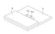
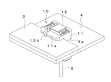
- a light bulb type lamp 1 shown in the figure includes a main body 2 that is attached to a lighting fixture, an LED substrate 3 on which an LED (not shown) is mounted on an upper surface, an attachment substrate 4 on which the LED substrate 3 is attached on an upper surface, It consists of a spherical cover 5 that covers the LED substrate 3 and the mounting substrate 4, and irradiates LED light to the outside via the cover 5.
- the main body 2 is formed of a hollow case having an opening on the upper surface, and a base 2a that is screwed into a socket (not shown) of a lighting fixture is provided at the lower end thereof.
- the base 2 a is connected to the LED substrate 3 via the cable 6, and external power is supplied from the base 2 a to the LED substrate 3.
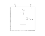
- the LED substrate 3 is formed in a quadrangular shape and fixed so as to overlap the upper surface of the mounting substrate 4.
- one LED or a plurality of chip-type LEDs formed in a planar shape is mounted on the LED substrate 3. 18, 17, and 20, only a part of the LED substrate 3 and the mounting substrate 4 is shown.
- the mounting substrate 4 is formed in a disc shape and is fixed to the upper surface of the main body 2.
- a connector 10 for connecting the cable 6 and the LED substrate 3 is attached to the attachment substrate 4, and the connector 10 is attached to an attachment hole 4 a provided in the attachment substrate 4.
- the mounting hole 4 a is a rectangular through-hole disposed on both ends of the LED substrate 3, and is formed so that one inner side surface in the width direction is flush with the end surface of the LED substrate 3.
- a concave portion 4b that engages with a part of the connector 10 to be described later is provided on the other inner surface in the width direction of the mounting hole 4a.
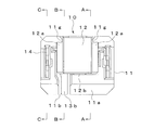
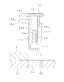
- the connector 10 includes a connector main body 11 inserted into the mounting hole 4 a of the mounting substrate 4, an upper surface cover 12 covering the upper surface of the connector main body 11, an electrical connection terminal 13 held by the connector main body 11, and the connector main body 11.
- the connector body 11 is made of a synthetic resin molded product, and is formed in a vertically long rectangular parallelepiped shape in which the dimension in the front-rear direction is smaller than the dimension in the width direction.
- An extension part 11a extending forward is provided on the upper surface side of the connector body 11, and a notch part 11b passing through one end side of the terminal 13 is provided near one end in the width direction of the extension part 11a.
- a terminal housing portion 11 c for housing the terminal 13 is provided in the connector main body 11, and the upper surface of the terminal housing portion 11 c is open to the upper surface of the connector main body 11.
- a circular insertion port 11d into which the cable 6 is inserted is provided near the other end in the width direction of the lower surface of the connector main body 11, and the insertion port 11d communicates with the terminal storage portion 11c.
- Holding holes 11e for holding the lock members 14 are provided on both sides in the width direction of the connector main body 11, and the holding holes 11e are opened in the front surface of the connector main body 11 so as to extend in the vertical direction.
- a rib 11 f that extends in the vertical direction protrudes from the back surface of the connector main body 11, and the rib 11 f is disposed at the center in the width direction of the connector main body 11.
- the upper surface cover 12 is formed in a rectangular flat plate shape covering the upper surface opening of the terminal accommodating portion 11c, and is attached to the upper surface side of the connector main body 11 by being attached to the connector main body 11 from the rear.
- Flange portions 12a extending in the front-rear direction are provided on both sides of the upper surface cover 12 in the width direction, and each flange portion 12a is connected to a pair of width direction locking portions 11g provided on the rear end side of the upper surface opening of the terminal storage portion 11c. It is designed to be locked from below.
- a protrusion 12b protruding forward is provided at the front end of the top cover 12, and the protrusion 12b engages with a hole 11h provided on the front end side of the top opening of the terminal storage portion 11c.
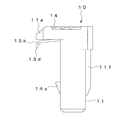
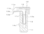
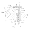
- the terminal 13 is made of a bent conductive metal plate, and is accommodated in the terminal accommodating portion 11c of the connector main body 11 from the upper surface opening of the terminal accommodating portion 11c.
- the terminal 13 includes a fixed piece portion 13a formed in a flat plate shape, a board connecting portion 13b extending from one end side in the width direction of the fixed piece portion 13a, and a cable extending from the other end side in the width direction of the fixed piece portion 13a. It consists of the connection part 13c.
- the fixed piece portion 13a is fixed to the terminal accommodating portion 11c by pressing both ends in the width direction against the inner surface of the terminal accommodating portion 11c.
- the board connecting portion 13b extends downward from the fixed piece 13a, is bent upward, and is further extended forward.
- the board connecting portion 13b is formed to be elastically deformable in the vertical direction (thickness direction of the LED board 3 and the mounting board 4), and a contact portion 13d that contacts the LED board 3 is bent downward at the tip thereof. Is provided.
- the cable connecting portion 13c extends downward from the fixed piece portion 13a, and a pair of first and second contact pieces 13e and 13f in the width direction that sandwich the conductive wire 6a of the cable 6 are opposed to each other on both sides in the width direction.
- Each contact piece 13e, 13f is formed to be opposed to each other by bending forward both sides in the width direction of an extending part 13g (predetermined part of the terminal body) extending downward from the fixed piece part 13a.
- the extending tip ends are formed obliquely so as to approach each other.
- the tip side of each contact piece 13e, 13f is formed to be elastically deformable in the width direction of the cable connecting portion 13c (opposite direction of each contact piece 13e, 13f).
- a first contact portion 13e-1 that bites into and comes into contact with the conducting wire 6a of the cable 6 is provided at the tip corner portion of the first contact piece 13e, and the first contact portion 13e-1 has an angle that is substantially perpendicular to the cross section. Consists of parts.
- a second contact portion 13f-1 that is slidably in surface contact with the conducting wire 6a of the cable 6 is provided at the tip of the second contact piece 13f.
- the second contact portion 13f-1 is a second contact piece. It is formed by chamfering the tip corner of 13f into a curved surface.
- the contact portions 13f-1 and 13e-1 are arranged to face each other in the width direction of the cable connection portion 13c (a direction orthogonal to the insertion direction of the cable 6).
- Each lock member 14 is made of a punched metal plate and is held in the holding hole 11e of the connector main body 11, respectively.
- the lock member 14 includes a fixed piece portion 14a extending from the upper end to the lower end in the holding hole 11e, an elastic piece portion 14b extending from the fixed piece portion 14a, and a locking portion provided at the tip of the elastic piece portion 14b. 14c, and the latching
- the fixed piece portion 14a is fixed to the holding hole 11e by pressing the front and rear ends on the upper end side and the front and rear ends on the lower end side against the inner surface of the holding hole 11e.
- the elastic piece portion 14b extends downward in front of the fixed piece portion 14a and is formed to bend upward.
- the locking portion 14c is formed so as to protrude forward from the tip of the elastic piece portion 14b, and protrudes forward of the connector body 11 from the opening of the holding hole 11e.
- the upper end of the locking portion 14c is formed horizontally, and the lower end side is formed obliquely so as to form a downward slope toward the rear.
- the connector body 11 When the connector 10 configured as described above is attached to the LED board 3 and the mounting board 4, the connector body 11 is inserted into the mounting hole 4a of the mounting board 4 from above as shown in FIG. At that time, the rib 11f of the connector body 11 engages with the recess 4b of the mounting hole 4a. Further, when the connector main body 11 is inserted, when the locking portion 14c of each lock member 14 comes into contact with the upper edge of the LED substrate 3, the elastic piece portion 14b is moved while the locking portion 14c moves backward due to the inclination of the lower end side. Is elastically deformed.
- the connector 10 in the mounting hole 4 a is brought into contact with the upper surface of the LED substrate 3 by the locking portion 14 c of each lock member 14 being locked to the lower surface of the mounting substrate 4. While being held in a state, movement in the vertical direction with respect to the LED substrate 3 and the mounting substrate 4 is restricted. Moreover, the movement of the connector 10 in the width direction is restricted by the engagement between the rib 11f of the connector main body 11 and the recess 4b of the mounting hole 4a.
- the cable 6 from which the coating of the leading end portion is removed to expose the conductive wire 6 a is inserted into the insertion port 11 d of the connector main body 11, and the cable 6 is connected to the terminal 13.
- the conductor 6a of the cable 6 is inserted between the contact pieces 13e and 13f of the cable connecting portion 13c, and the contact pieces 13e and 13f are pushed and spread while contacting the conductor 6a.
- each contact piece 13e and 13f press-contacts to the conducting wire 6a, and the cable 6 is connected to the terminal 13.
- the contact portion 13e-1 of the first contact piece 13e comes into contact with the lead wire 6a, the movement of the lead wire 6a in the anti-insertion direction is restricted, and the lead wire 6a is prevented from coming off.
- the second contact portion 13f-1 of the second contact piece 13f is slidably surface-contacted without entering the conductor 6a, the contact area between the second contact piece 13f and the conductor 6a is sufficient. Secured. In this case, since the first and second contact portions 13e-1, 13f-1 are arranged to face each other in a direction orthogonal to the insertion direction of the conductor 6a, the contact portions 13e-1, 13f- 1 is applied to the same position in the axial direction of the conducting wire 6a.
- a pair of connectors 10 are attached to the LED board 3 and the mounting board 4 as shown in FIG. 21, and the cable 6 connected to one connector 10 is connected to the plus electrode of the base 2 a and connected to the other connector 10. The cable 6 thus connected is connected to the negative electrode of the base 2a.
- the board connecting portion 13b and the LED board 3 are electrically connected by contacting the board connecting portion 13b formed on the terminal 13 so as to be elastically deformable in the vertical direction to the upper surface of the LED board 3.
- the substrate connecting portion 13b of the terminal 13 is held in pressure contact with the upper surface of the LED substrate 3.
- the terminal 13 can be easily connected to the LED substrate 3 without being soldered, and the connector 10 can be attached very easily.
- the locking portions 14c of the lock members 14 are elastically deformed while coming into contact with the edges of the mounting holes 4a, so that the locking portions 14c become the mounting holes 4a. Since the locking portion 14c is restored and locked to the lower surface of the mounting substrate 4 when the edge portion of the locking portion 14c is overcome, the insertion resistance to the mounting hole 4a can be reduced by elastic deformation of the locking portion 14c. At the same time, the locking portion 14c can be reliably locked to the lower surface of the mounting substrate 4 by restoring the locking portion 14c.
- a terminal accommodating portion 11 c that accommodates the terminal 13 from an opening located on the upper surface side of the LED substrate 3 is provided in the connector main body 11, and the upper surface opening of the terminal accommodating portion 11 c is provided by the upper surface cover 12 attached to the connector main body 11. Since the inside of the terminal accommodating portion 11c is not exposed on the upper surface of the connector main body 11, the light of the LED can be reliably reflected by the upper surface of the connector main body 11 and the upper surface cover 12. At that time, by making the upper surface of the connector main body 11 and the upper surface cover 12 have a highly reflective color, even if the upper surface side of the connector main body 11 is arranged on the upper surface of the LED substrate 3, the upper surface side of the LED substrate 3 is the connector main body 11. Therefore, there is an advantage that it is not darkened and the lighting effect is not lowered.
- the terminal 13 is integrally provided with the cable connecting portion 13c to which the cable 6 can be connected from the outside, it is not necessary to separately provide a terminal for connecting the cable, and the number of parts can be reduced.
- a first contact portion 13e-1 is provided at the tip corner of the first contact piece 13e of the terminal 13 to restrict the movement of the conductor 6a in the anti-insertion direction by biting into the conductor 6a of the cable 6. Since the second contact portion 13f-1 with which the conducting wire 6a is slidably contacted is provided at the tip of the second contact piece 13f of the terminal 13, the conducting wire 6a is removed by the first contact portion 13e-1. In addition to the prevention, the second contact portion 13f-1 can ensure a sufficient contact area with the conductor 6a, and can reliably hold the conductor 6a without deteriorating connection reliability.
- the second contact portion 13f-1 is formed by chamfering the tip end corner portion of the second contact piece 13f, the tip end side of the second contact piece 13f is bent to form a curved contact portion.
- the second contact piece 13f can be easily formed with a simple shape.
- first and second contact portions 13e-1 and 13f-1 are arranged so as to face each other in a direction orthogonal to the insertion direction of the conductor 6a, the pressing portions from the contact portions 13e-1 and 13f-1 are arranged. Pressure can be applied to the same position in the axial direction of the conducting wire 6a, and the conducting wire 6a can be securely held by the contact portions 13e and 13f.
- first and second contact pieces 13e and 13f are formed by bending both sides of the extending portion 13g of the terminal 13 so as to face each other, the contact pieces 13e and 13f can be easily formed. And productivity can be improved.
- the connector 10 connected to the LED substrate 3 of the light bulb type lamp is shown.
- the present invention is not limited to the substrate for the light bulb type lamp, and the connector is connected to the substrate of another device. It can also be applied to.
- the electrical connection terminal of this invention is applied also to the terminal etc. which are directly attached to another kind of connector, a board
- SYMBOLS 1 Light bulb type lamp, 3 ... LED board, 4 ... Mounting board, 4a ... Mounting hole, 6 ... Cable, 10 ... Connector, 11 ... Connector main body, 11c ... Terminal storage part, 12 ... Top cover, 13 ... Terminal, 13b ... Board connection part, 13c... Cable connection part, 13e... First contact piece, 13f... Second contact piece, 13e-1 ... First contact part, 13f-1 ... Second contact part.
Landscapes
- Coupling Device And Connection With Printed Circuit (AREA)
- Details Of Connecting Devices For Male And Female Coupling (AREA)
Abstract
Description
Claims (5)
- 互いに厚さ方向に対向して配置された第1の接触片及び第2の接触片を備え、第1及び第2の接触片の間に接続対象物を挿入することにより、各接触片を介して接続対象物と接続する電気接続用端子において、
前記第1及び第2の接触片を、接続対象物の挿入方向に向かって延びる先端側が互いに接近するように斜めに形成するとともに、それぞれ対向方向に弾性変形可能に形成し、
第1の接触片の先端角部に、接続対象物に食い込むことにより接続対象物の反挿入方向への移動を規制する第1の接触部を設け、
第2の接触片の先端には、接続対象物が摺動自在に接触する第2の接触部を設けるとともに、第2の接触部を第2の接触片の先端角部を面取りすることによって形成した
ことを特徴とする電気接続用端子。 - 前記第1及び第2の接触部を互いに接続対象物の挿入方向に直交する方向に対向するように配置した
ことを特徴とする請求項1記載の電気接続用端子。 - 前記第1及び第2の接触片を端子本体の所定部分の両側を互いに対向するように曲げ起こすことによって形成した
ことを特徴とする請求項1または2記載の電気接続用端子。 - 前記接続対象物は導線である
ことを特徴とする請求項1、2または3記載の電気接続用端子。 - 請求項1、2、3または4記載の電気接続用端子を備えた
ことを特徴とするコネクタ。
Priority Applications (4)
| Application Number | Priority Date | Filing Date | Title |
|---|---|---|---|
| CN201280002634XA CN103081231A (zh) | 2011-01-12 | 2012-01-11 | 电连接用端子及使用其的连接器 |
| US13/819,502 US8808025B2 (en) | 2011-01-12 | 2012-01-11 | Electrical connection terminal and connector using same |
| KR1020137004064A KR101406247B1 (ko) | 2011-01-12 | 2012-01-11 | 전기 접속용 단자 및 이것을 이용한 커넥터 |
| EP12734468.7A EP2665130A4 (en) | 2011-01-12 | 2012-01-11 | ELECTRICAL CONNECTING TERMINAL AND ELECTRICAL CONNECTION THEREWITH |
Applications Claiming Priority (2)
| Application Number | Priority Date | Filing Date | Title |
|---|---|---|---|
| JP2011004054A JP4838902B1 (ja) | 2011-01-12 | 2011-01-12 | 電気接続用端子及びこれを用いたコネクタ |
| JP2011-004054 | 2011-01-12 |
Publications (1)
| Publication Number | Publication Date |
|---|---|
| WO2012096286A1 true WO2012096286A1 (ja) | 2012-07-19 |
Family
ID=45418244
Family Applications (1)
| Application Number | Title | Priority Date | Filing Date |
|---|---|---|---|
| PCT/JP2012/050337 WO2012096286A1 (ja) | 2011-01-12 | 2012-01-11 | 電気接続用端子及びこれを用いたコネクタ |
Country Status (7)
| Country | Link |
|---|---|
| US (1) | US8808025B2 (ja) |
| EP (1) | EP2665130A4 (ja) |
| JP (1) | JP4838902B1 (ja) |
| KR (1) | KR101406247B1 (ja) |
| CN (1) | CN103081231A (ja) |
| TW (1) | TWI594516B (ja) |
| WO (1) | WO2012096286A1 (ja) |
Families Citing this family (5)
| Publication number | Priority date | Publication date | Assignee | Title |
|---|---|---|---|---|
| CN103196042B (zh) * | 2012-01-10 | 2016-08-24 | 欧司朗股份有限公司 | 照明装置及其制造方法 |
| US10066814B2 (en) | 2012-01-11 | 2018-09-04 | Te Connectivity Corporation | Solid state lighting assembly |
| TWM462333U (zh) * | 2013-02-05 | 2013-09-21 | Hep Tech Co Ltd | 可調光之發光二極體燈具 |
| JP6286791B2 (ja) * | 2013-12-10 | 2018-03-07 | パナソニックIpマネジメント株式会社 | 光源ユニット及びそれを用いた照明器具 |
| CN103883995B (zh) * | 2014-03-28 | 2017-07-18 | 木林森股份有限公司 | 易于装配的cob灯珠、灯珠支架和灯珠制作方法、装配简单的led模组 |
Citations (6)
| Publication number | Priority date | Publication date | Assignee | Title |
|---|---|---|---|---|
| JPH0590823U (ja) | 1992-05-19 | 1993-12-10 | アルプス電気株式会社 | コネクタ装置 |
| JPH07272812A (ja) | 1994-03-29 | 1995-10-20 | Hosiden Corp | 速結タイプ陰極線管ソケット |
| JPH0950837A (ja) | 1995-08-07 | 1997-02-18 | Hosiden Corp | リード線速結コネクタ |
| JPH10340745A (ja) * | 1997-06-04 | 1998-12-22 | Kyoshin Kogyo Kk | ワンタッチコネクタおよびワンタッチコネクタ組合せ体 |
| JP2005004965A (ja) * | 2002-07-26 | 2005-01-06 | Matsushita Electric Works Ltd | 配線器具 |
| JP2010033959A (ja) | 2008-07-30 | 2010-02-12 | Toshiba Lighting & Technology Corp | 電球型ランプ |
Family Cites Families (7)
| Publication number | Priority date | Publication date | Assignee | Title |
|---|---|---|---|---|
| JP2000124014A (ja) * | 1998-10-19 | 2000-04-28 | Hokuriku Electric Ind Co Ltd | 電気部品ユニット |
| US6276955B1 (en) * | 2000-01-14 | 2001-08-21 | Avaya Technology Corp. | Multi contact socket connector |
| DE20112090U1 (de) * | 2001-07-20 | 2001-09-13 | Phoenix Contact GmbH & Co. KG, 32825 Blomberg | Klemmelement mit einem Hülsenkörper zum abisolierfreien Anschluß eines elektrischen Leiters |
| CN100403609C (zh) * | 2002-07-26 | 2008-07-16 | 松下电工株式会社 | 布线器具 |
| DE202006003400U1 (de) * | 2006-03-04 | 2007-07-12 | Weidmüller Interface GmbH & Co. KG | Anschlusssystem mit Direktsteckanschluss |
| US7722382B2 (en) * | 2006-11-02 | 2010-05-25 | Tyco Electronics Corporation | Wire retention connector system |
| CN102175000B (zh) * | 2008-07-30 | 2013-11-06 | 东芝照明技术株式会社 | 灯装置及照明器具 |
-
2011
- 2011-01-12 JP JP2011004054A patent/JP4838902B1/ja not_active Expired - Fee Related
-
2012
- 2012-01-11 KR KR1020137004064A patent/KR101406247B1/ko not_active IP Right Cessation
- 2012-01-11 US US13/819,502 patent/US8808025B2/en not_active Expired - Fee Related
- 2012-01-11 CN CN201280002634XA patent/CN103081231A/zh active Pending
- 2012-01-11 TW TW101101043A patent/TWI594516B/zh not_active IP Right Cessation
- 2012-01-11 WO PCT/JP2012/050337 patent/WO2012096286A1/ja active Application Filing
- 2012-01-11 EP EP12734468.7A patent/EP2665130A4/en not_active Withdrawn
Patent Citations (6)
| Publication number | Priority date | Publication date | Assignee | Title |
|---|---|---|---|---|
| JPH0590823U (ja) | 1992-05-19 | 1993-12-10 | アルプス電気株式会社 | コネクタ装置 |
| JPH07272812A (ja) | 1994-03-29 | 1995-10-20 | Hosiden Corp | 速結タイプ陰極線管ソケット |
| JPH0950837A (ja) | 1995-08-07 | 1997-02-18 | Hosiden Corp | リード線速結コネクタ |
| JPH10340745A (ja) * | 1997-06-04 | 1998-12-22 | Kyoshin Kogyo Kk | ワンタッチコネクタおよびワンタッチコネクタ組合せ体 |
| JP2005004965A (ja) * | 2002-07-26 | 2005-01-06 | Matsushita Electric Works Ltd | 配線器具 |
| JP2010033959A (ja) | 2008-07-30 | 2010-02-12 | Toshiba Lighting & Technology Corp | 電球型ランプ |
Non-Patent Citations (1)
| Title |
|---|
| See also references of EP2665130A4 |
Also Published As
| Publication number | Publication date |
|---|---|
| CN103081231A (zh) | 2013-05-01 |
| US8808025B2 (en) | 2014-08-19 |
| EP2665130A1 (en) | 2013-11-20 |
| KR101406247B1 (ko) | 2014-06-12 |
| EP2665130A4 (en) | 2014-06-18 |
| US20130288514A1 (en) | 2013-10-31 |
| JP2012146515A (ja) | 2012-08-02 |
| TW201230528A (en) | 2012-07-16 |
| JP4838902B1 (ja) | 2011-12-14 |
| KR20130056286A (ko) | 2013-05-29 |
| TWI594516B (zh) | 2017-08-01 |
Similar Documents
| Publication | Publication Date | Title |
|---|---|---|
| WO2012096288A1 (ja) | コネクタ | |
| US8851903B2 (en) | Connector assemblies for connector systems | |
| US7637787B2 (en) | Audio jack connector | |
| US8475000B2 (en) | Connector, and LED lighting apparatus using the connector | |
| JP5718631B2 (ja) | 電子部品の接続構造 | |
| US8942007B2 (en) | Electrical component | |
| JP5351065B2 (ja) | Ledランプユニット | |
| US20100155135A1 (en) | Illumination unit | |
| US7850466B2 (en) | Through board inverted connector | |
| WO2012096286A1 (ja) | 電気接続用端子及びこれを用いたコネクタ | |
| TWI734968B (zh) | 電連接器及電連接器組 | |
| CN105591220B (zh) | 电路板接线端子和包括电路板接线端子的连接插座 | |
| TW201513469A (zh) | 線狀導體連接用端子 | |
| US8465314B2 (en) | Card edge connector | |
| TW202112005A (zh) | 安全、堅固且緊密之連接器 | |
| US7247041B2 (en) | Land grid array connector | |
| JP2007157408A (ja) | コネクタ | |
| WO2016021249A1 (ja) | コネクタ | |
| JP5177687B2 (ja) | 速結端子、端子台および照明器具 | |
| JP4611850B2 (ja) | 端子台 | |
| JP2017117562A (ja) | 金属端子 | |
| CN112740486A (zh) | 连接器及基板单元 | |
| JP2009272130A (ja) | 基板用コネクタ |
Legal Events
| Date | Code | Title | Description |
|---|---|---|---|
| WWE | Wipo information: entry into national phase |
Ref document number: 201280002634.X Country of ref document: CN |
|
| 121 | Ep: the epo has been informed by wipo that ep was designated in this application |
Ref document number: 12734468 Country of ref document: EP Kind code of ref document: A1 |
|
| ENP | Entry into the national phase |
Ref document number: 20137004064 Country of ref document: KR Kind code of ref document: A |
|
| WWE | Wipo information: entry into national phase |
Ref document number: 13819502 Country of ref document: US Ref document number: 2012734468 Country of ref document: EP |
|
| NENP | Non-entry into the national phase |
Ref country code: DE |