WO2012093574A1 - 剥離装置、剥離システム、剥離方法及びコンピュータ記憶媒体 - Google Patents
剥離装置、剥離システム、剥離方法及びコンピュータ記憶媒体 Download PDFInfo
- Publication number
- WO2012093574A1 WO2012093574A1 PCT/JP2011/079187 JP2011079187W WO2012093574A1 WO 2012093574 A1 WO2012093574 A1 WO 2012093574A1 JP 2011079187 W JP2011079187 W JP 2011079187W WO 2012093574 A1 WO2012093574 A1 WO 2012093574A1
- Authority
- WO
- WIPO (PCT)
- Prior art keywords
- substrate
- processed
- wafer
- peeling
- inert gas
- Prior art date
- Legal status (The legal status is an assumption and is not a legal conclusion. Google has not performed a legal analysis and makes no representation as to the accuracy of the status listed.)
- Ceased
Links
Images












Classifications
-
- B—PERFORMING OPERATIONS; TRANSPORTING
- B32—LAYERED PRODUCTS
- B32B—LAYERED PRODUCTS, i.e. PRODUCTS BUILT-UP OF STRATA OF FLAT OR NON-FLAT, e.g. CELLULAR OR HONEYCOMB, FORM
- B32B38/00—Ancillary operations in connection with laminating processes
- B32B38/10—Removing layers, or parts of layers, mechanically or chemically
-
- B—PERFORMING OPERATIONS; TRANSPORTING
- B32—LAYERED PRODUCTS
- B32B—LAYERED PRODUCTS, i.e. PRODUCTS BUILT-UP OF STRATA OF FLAT OR NON-FLAT, e.g. CELLULAR OR HONEYCOMB, FORM
- B32B43/00—Operations specially adapted for layered products and not otherwise provided for, e.g. repairing; Apparatus therefor
- B32B43/006—Delaminating
-
- H—ELECTRICITY
- H10—SEMICONDUCTOR DEVICES; ELECTRIC SOLID-STATE DEVICES NOT OTHERWISE PROVIDED FOR
- H10P—GENERIC PROCESSES OR APPARATUS FOR THE MANUFACTURE OR TREATMENT OF DEVICES COVERED BY CLASS H10
- H10P14/00—Formation of materials, e.g. in the shape of layers or pillars
- H10P14/20—Formation of materials, e.g. in the shape of layers or pillars of semiconductor materials
-
- H—ELECTRICITY
- H10—SEMICONDUCTOR DEVICES; ELECTRIC SOLID-STATE DEVICES NOT OTHERWISE PROVIDED FOR
- H10P—GENERIC PROCESSES OR APPARATUS FOR THE MANUFACTURE OR TREATMENT OF DEVICES COVERED BY CLASS H10
- H10P72/00—Handling or holding of wafers, substrates or devices during manufacture or treatment thereof
- H10P72/04—Apparatus for manufacture or treatment
- H10P72/0402—Apparatus for fluid treatment
- H10P72/0406—Apparatus for fluid treatment for cleaning followed by drying, rinsing, stripping, blasting or the like
- H10P72/0411—Apparatus for fluid treatment for cleaning followed by drying, rinsing, stripping, blasting or the like for wet cleaning or washing
- H10P72/0414—Apparatus for fluid treatment for cleaning followed by drying, rinsing, stripping, blasting or the like for wet cleaning or washing using mainly spraying means, e.g. nozzles
-
- H—ELECTRICITY
- H10—SEMICONDUCTOR DEVICES; ELECTRIC SOLID-STATE DEVICES NOT OTHERWISE PROVIDED FOR
- H10P—GENERIC PROCESSES OR APPARATUS FOR THE MANUFACTURE OR TREATMENT OF DEVICES COVERED BY CLASS H10
- H10P72/00—Handling or holding of wafers, substrates or devices during manufacture or treatment thereof
- H10P72/04—Apparatus for manufacture or treatment
- H10P72/0428—Apparatus for mechanical treatment or grinding or cutting
-
- H—ELECTRICITY
- H10—SEMICONDUCTOR DEVICES; ELECTRIC SOLID-STATE DEVICES NOT OTHERWISE PROVIDED FOR
- H10P—GENERIC PROCESSES OR APPARATUS FOR THE MANUFACTURE OR TREATMENT OF DEVICES COVERED BY CLASS H10
- H10P72/00—Handling or holding of wafers, substrates or devices during manufacture or treatment thereof
- H10P72/04—Apparatus for manufacture or treatment
- H10P72/0431—Apparatus for thermal treatment
- H10P72/0432—Apparatus for thermal treatment mainly by conduction
-
- H—ELECTRICITY
- H10—SEMICONDUCTOR DEVICES; ELECTRIC SOLID-STATE DEVICES NOT OTHERWISE PROVIDED FOR
- H10P—GENERIC PROCESSES OR APPARATUS FOR THE MANUFACTURE OR TREATMENT OF DEVICES COVERED BY CLASS H10
- H10P72/00—Handling or holding of wafers, substrates or devices during manufacture or treatment thereof
- H10P72/70—Handling or holding of wafers, substrates or devices during manufacture or treatment thereof for supporting or gripping
- H10P72/76—Handling or holding of wafers, substrates or devices during manufacture or treatment thereof for supporting or gripping using mechanical means, e.g. clamps or pinches
- H10P72/7604—Handling or holding of wafers, substrates or devices during manufacture or treatment thereof for supporting or gripping using mechanical means, e.g. clamps or pinches the wafers being placed on a susceptor, stage or support
- H10P72/7608—Handling or holding of wafers, substrates or devices during manufacture or treatment thereof for supporting or gripping using mechanical means, e.g. clamps or pinches the wafers being placed on a susceptor, stage or support characterised by a plurality of separate clamping members, e.g. clamping fingers
-
- B—PERFORMING OPERATIONS; TRANSPORTING
- B32—LAYERED PRODUCTS
- B32B—LAYERED PRODUCTS, i.e. PRODUCTS BUILT-UP OF STRATA OF FLAT OR NON-FLAT, e.g. CELLULAR OR HONEYCOMB, FORM
- B32B2309/00—Parameters for the laminating or treatment process; Apparatus details
- B32B2309/60—In a particular environment
- B32B2309/68—Vacuum
-
- B—PERFORMING OPERATIONS; TRANSPORTING
- B32—LAYERED PRODUCTS
- B32B—LAYERED PRODUCTS, i.e. PRODUCTS BUILT-UP OF STRATA OF FLAT OR NON-FLAT, e.g. CELLULAR OR HONEYCOMB, FORM
- B32B2310/00—Treatment by energy or chemical effects
- B32B2310/04—Treatment by energy or chemical effects using liquids, gas or steam
- B32B2310/0445—Treatment by energy or chemical effects using liquids, gas or steam using gas or flames
- B32B2310/0463—Treatment by energy or chemical effects using liquids, gas or steam using gas or flames other than air
- B32B2310/0472—Treatment by energy or chemical effects using liquids, gas or steam using gas or flames other than air inert gas
-
- B—PERFORMING OPERATIONS; TRANSPORTING
- B32—LAYERED PRODUCTS
- B32B—LAYERED PRODUCTS, i.e. PRODUCTS BUILT-UP OF STRATA OF FLAT OR NON-FLAT, e.g. CELLULAR OR HONEYCOMB, FORM
- B32B2457/00—Electrical equipment
- B32B2457/14—Semiconductor wafers
-
- B—PERFORMING OPERATIONS; TRANSPORTING
- B32—LAYERED PRODUCTS
- B32B—LAYERED PRODUCTS, i.e. PRODUCTS BUILT-UP OF STRATA OF FLAT OR NON-FLAT, e.g. CELLULAR OR HONEYCOMB, FORM
- B32B37/00—Methods or apparatus for laminating, e.g. by curing or by ultrasonic bonding
- B32B37/06—Methods or apparatus for laminating, e.g. by curing or by ultrasonic bonding characterised by the heating method
-
- B—PERFORMING OPERATIONS; TRANSPORTING
- B32—LAYERED PRODUCTS
- B32B—LAYERED PRODUCTS, i.e. PRODUCTS BUILT-UP OF STRATA OF FLAT OR NON-FLAT, e.g. CELLULAR OR HONEYCOMB, FORM
- B32B41/00—Arrangements for controlling or monitoring lamination processes; Safety arrangements
-
- H—ELECTRICITY
- H10—SEMICONDUCTOR DEVICES; ELECTRIC SOLID-STATE DEVICES NOT OTHERWISE PROVIDED FOR
- H10P—GENERIC PROCESSES OR APPARATUS FOR THE MANUFACTURE OR TREATMENT OF DEVICES COVERED BY CLASS H10
- H10P72/00—Handling or holding of wafers, substrates or devices during manufacture or treatment thereof
- H10P72/70—Handling or holding of wafers, substrates or devices during manufacture or treatment thereof for supporting or gripping
- H10P72/74—Handling or holding of wafers, substrates or devices during manufacture or treatment thereof for supporting or gripping using temporarily an auxiliary support
- H10P72/744—Details of chemical or physical process used for separating the auxiliary support from a device or a wafer
-
- Y—GENERAL TAGGING OF NEW TECHNOLOGICAL DEVELOPMENTS; GENERAL TAGGING OF CROSS-SECTIONAL TECHNOLOGIES SPANNING OVER SEVERAL SECTIONS OF THE IPC; TECHNICAL SUBJECTS COVERED BY FORMER USPC CROSS-REFERENCE ART COLLECTIONS [XRACs] AND DIGESTS
- Y10—TECHNICAL SUBJECTS COVERED BY FORMER USPC
- Y10S—TECHNICAL SUBJECTS COVERED BY FORMER USPC CROSS-REFERENCE ART COLLECTIONS [XRACs] AND DIGESTS
- Y10S156/00—Adhesive bonding and miscellaneous chemical manufacture
- Y10S156/918—Delaminating processes adapted for specified product, e.g. delaminating medical specimen slide
- Y10S156/93—Semiconductive product delaminating, e.g. delaminating emiconductive wafer from underlayer
-
- Y—GENERAL TAGGING OF NEW TECHNOLOGICAL DEVELOPMENTS; GENERAL TAGGING OF CROSS-SECTIONAL TECHNOLOGIES SPANNING OVER SEVERAL SECTIONS OF THE IPC; TECHNICAL SUBJECTS COVERED BY FORMER USPC CROSS-REFERENCE ART COLLECTIONS [XRACs] AND DIGESTS
- Y10—TECHNICAL SUBJECTS COVERED BY FORMER USPC
- Y10S—TECHNICAL SUBJECTS COVERED BY FORMER USPC CROSS-REFERENCE ART COLLECTIONS [XRACs] AND DIGESTS
- Y10S156/00—Adhesive bonding and miscellaneous chemical manufacture
- Y10S156/934—Apparatus having delaminating means adapted for delaminating a specified article
- Y10S156/941—Means for delaminating semiconductive product
-
- Y—GENERAL TAGGING OF NEW TECHNOLOGICAL DEVELOPMENTS; GENERAL TAGGING OF CROSS-SECTIONAL TECHNOLOGIES SPANNING OVER SEVERAL SECTIONS OF THE IPC; TECHNICAL SUBJECTS COVERED BY FORMER USPC CROSS-REFERENCE ART COLLECTIONS [XRACs] AND DIGESTS
- Y10—TECHNICAL SUBJECTS COVERED BY FORMER USPC
- Y10T—TECHNICAL SUBJECTS COVERED BY FORMER US CLASSIFICATION
- Y10T156/00—Adhesive bonding and miscellaneous chemical manufacture
- Y10T156/11—Methods of delaminating, per se; i.e., separating at bonding face
- Y10T156/1126—Using direct fluid current against work during delaminating
-
- Y—GENERAL TAGGING OF NEW TECHNOLOGICAL DEVELOPMENTS; GENERAL TAGGING OF CROSS-SECTIONAL TECHNOLOGIES SPANNING OVER SEVERAL SECTIONS OF THE IPC; TECHNICAL SUBJECTS COVERED BY FORMER USPC CROSS-REFERENCE ART COLLECTIONS [XRACs] AND DIGESTS
- Y10—TECHNICAL SUBJECTS COVERED BY FORMER USPC
- Y10T—TECHNICAL SUBJECTS COVERED BY FORMER US CLASSIFICATION
- Y10T156/00—Adhesive bonding and miscellaneous chemical manufacture
- Y10T156/11—Methods of delaminating, per se; i.e., separating at bonding face
- Y10T156/1126—Using direct fluid current against work during delaminating
- Y10T156/1137—Using air blast directly against work during delaminating
-
- Y—GENERAL TAGGING OF NEW TECHNOLOGICAL DEVELOPMENTS; GENERAL TAGGING OF CROSS-SECTIONAL TECHNOLOGIES SPANNING OVER SEVERAL SECTIONS OF THE IPC; TECHNICAL SUBJECTS COVERED BY FORMER USPC CROSS-REFERENCE ART COLLECTIONS [XRACs] AND DIGESTS
- Y10—TECHNICAL SUBJECTS COVERED BY FORMER USPC
- Y10T—TECHNICAL SUBJECTS COVERED BY FORMER US CLASSIFICATION
- Y10T156/00—Adhesive bonding and miscellaneous chemical manufacture
- Y10T156/11—Methods of delaminating, per se; i.e., separating at bonding face
- Y10T156/1153—Temperature change for delamination [e.g., heating during delaminating, etc.]
-
- Y—GENERAL TAGGING OF NEW TECHNOLOGICAL DEVELOPMENTS; GENERAL TAGGING OF CROSS-SECTIONAL TECHNOLOGIES SPANNING OVER SEVERAL SECTIONS OF THE IPC; TECHNICAL SUBJECTS COVERED BY FORMER USPC CROSS-REFERENCE ART COLLECTIONS [XRACs] AND DIGESTS
- Y10—TECHNICAL SUBJECTS COVERED BY FORMER USPC
- Y10T—TECHNICAL SUBJECTS COVERED BY FORMER US CLASSIFICATION
- Y10T156/00—Adhesive bonding and miscellaneous chemical manufacture
- Y10T156/11—Methods of delaminating, per se; i.e., separating at bonding face
- Y10T156/1168—Gripping and pulling work apart during delaminating
- Y10T156/1189—Gripping and pulling work apart during delaminating with shearing during delaminating
-
- Y—GENERAL TAGGING OF NEW TECHNOLOGICAL DEVELOPMENTS; GENERAL TAGGING OF CROSS-SECTIONAL TECHNOLOGIES SPANNING OVER SEVERAL SECTIONS OF THE IPC; TECHNICAL SUBJECTS COVERED BY FORMER USPC CROSS-REFERENCE ART COLLECTIONS [XRACs] AND DIGESTS
- Y10—TECHNICAL SUBJECTS COVERED BY FORMER USPC
- Y10T—TECHNICAL SUBJECTS COVERED BY FORMER US CLASSIFICATION
- Y10T156/00—Adhesive bonding and miscellaneous chemical manufacture
- Y10T156/19—Delaminating means
- Y10T156/1911—Heating or cooling delaminating means [e.g., melting means, freezing means, etc.]
-
- Y—GENERAL TAGGING OF NEW TECHNOLOGICAL DEVELOPMENTS; GENERAL TAGGING OF CROSS-SECTIONAL TECHNOLOGIES SPANNING OVER SEVERAL SECTIONS OF THE IPC; TECHNICAL SUBJECTS COVERED BY FORMER USPC CROSS-REFERENCE ART COLLECTIONS [XRACs] AND DIGESTS
- Y10—TECHNICAL SUBJECTS COVERED BY FORMER USPC
- Y10T—TECHNICAL SUBJECTS COVERED BY FORMER US CLASSIFICATION
- Y10T156/00—Adhesive bonding and miscellaneous chemical manufacture
- Y10T156/19—Delaminating means
- Y10T156/1928—Differential fluid pressure delaminating means
- Y10T156/1933—Spraying delaminating means [e.g., atomizer, etc.
- Y10T156/1939—Air blasting delaminating means]
-
- Y—GENERAL TAGGING OF NEW TECHNOLOGICAL DEVELOPMENTS; GENERAL TAGGING OF CROSS-SECTIONAL TECHNOLOGIES SPANNING OVER SEVERAL SECTIONS OF THE IPC; TECHNICAL SUBJECTS COVERED BY FORMER USPC CROSS-REFERENCE ART COLLECTIONS [XRACs] AND DIGESTS
- Y10—TECHNICAL SUBJECTS COVERED BY FORMER USPC
- Y10T—TECHNICAL SUBJECTS COVERED BY FORMER US CLASSIFICATION
- Y10T156/00—Adhesive bonding and miscellaneous chemical manufacture
- Y10T156/19—Delaminating means
- Y10T156/1961—Severing delaminating means [e.g., chisel, etc.]
- Y10T156/1967—Cutting delaminating means
- Y10T156/1972—Shearing delaminating means
Definitions
- the present invention relates to a peeling apparatus that peels a superposed substrate from a substrate to be processed and a support substrate, a peeling system including the peeling apparatus, a peeling method using the peeling apparatus, and a computer storage medium.
- the diameter of a semiconductor wafer (hereinafter referred to as “wafer”) has been increased. Further, in a specific process such as mounting, it is required to make the wafer thinner. For example, if a thin wafer with a large diameter is transported or polished as it is, the wafer may be warped or cracked. For this reason, for example, in order to reinforce the wafer, the wafer is attached to, for example, a wafer that is a support substrate or a glass substrate. Then, after a predetermined process such as a wafer polishing process is performed in a state where the wafer and the support substrate are bonded in this way, the wafer and the support substrate are peeled off.
- a predetermined process such as a wafer polishing process is performed in a state where the wafer and the support substrate are bonded in this way, the wafer and the support substrate are peeled off.
- Patent Document 1 proposes a peeling apparatus that directly bonds a wafer on which a device is formed to a wafer on which a thermal oxide film is formed, and then peels the wafer.
- This peeling apparatus has, for example, a first holder that holds a wafer, a second holder that holds a support substrate, and a nozzle that ejects liquid between the wafer and the support substrate.
- the jet pressure preferably the bonding pressure between the wafer and the support substrate, which is bonded from the nozzle, that is, the bonding pressure between the wafer and the support substrate is larger than the bonding strength between the wafer and the support substrate. Separation of the wafer and the support substrate is performed by ejecting the liquid with an ejection pressure that is twice or more larger than the strength.
- the present invention has been made in view of the above points, and efficiently suppresses rapid progress of oxidation at the bonding surface of the substrate during the separation treatment between the substrate to be processed and the supporting substrate accompanied by heat treatment.
- the purpose is to do.
- the present invention provides a peeling apparatus for peeling a polymerized substrate in which a substrate to be processed and a support substrate are bonded with an adhesive into a substrate to be processed and a support substrate, and heating the substrate to be processed.
- An inert gas supply mechanism for supplying an inert gas to the exposed joint surface of the substrate to be processed, the inert gas supply mechanism including a porous portion in which a plurality of holes are formed, and the porous Is connected to the porous portion, and the inert gas is supplied to the porous portion. It has a gas supply tube, wherein the porous portion is provided with a predetermined distance in the vertical direction from the bonding surface of the substrate to be processed.
- an inert gas supply provided with a moving mechanism for moving the first holding part or the second holding part relatively in the horizontal direction and a porous part to which a gas supply pipe is connected. Since the porous portion is provided at a predetermined distance in the vertical direction from the bonding surface between the substrate to be processed and the support substrate, for example, the second holding portion is moved in the horizontal direction by the moving mechanism. In this way, the substrate to be processed held by the first holding unit and the support substrate held by the second holding unit can be peeled off, and further, on the bonding surface of the substrate to be processed exposed by peeling.
- the inert gas can be supplied from the porous portion.
- the inert gas is supplied through the porous portion in which a plurality of holes are formed, the flow rate of the supplied inert gas is suppressed. Accordingly, when supplying the inert gas, ambient air is not involved and only the inert gas is supplied to the bonding surface of the wafer to be processed W, so that the exposed bonding surface of the substrate to be processed is inert gas. Atmosphere. For this reason, for example, in order to suppress oxidation of the bonding surface of the heated substrate to be processed, it is not necessary to take a major measure of covering the substrate to be processed with an airtight container or the like. Therefore, according to the present invention, it is possible to efficiently suppress the rapid progress of oxidation at the bonding surface of the substrates, which occurs when the heat-treated substrate and the support substrate are peeled off.
- a separation system for separating a polymerized substrate in which a substrate to be processed and a support substrate are bonded with an adhesive to the substrate to be processed and the support substrate.
- a peeling processing station for performing a predetermined process, a loading / unloading station for loading / unloading a substrate to be processed, a support substrate or a polymerization substrate with respect to the peeling processing station, and between the peeling processing station and the loading / unloading station,
- a transfer device that transfers the substrate to be processed, the support substrate, or the polymerization substrate, and the peeling processing station includes a peeling device that peels the polymerization substrate from the substrate to be processed and the support substrate, and a substrate peeled by the peeling device.
- the peeling device heats the substrate to be processed.
- An inert gas supply mechanism for supplying an inert gas to the exposed joint surface of the substrate to be processed, the inert gas supply mechanism including a porous portion in which a plurality of holes are formed, and the porous And a gas supply pipe for supplying an inert gas to the porous portion, and the porous portion is provided at a predetermined distance from the bonding surface of the substrate to be processed in a vertical direction. ing.
- the present invention is a peeling method in which a substrate to be processed and a support substrate are bonded to each other with an adhesive using a peeling device to peel the polymerization substrate into the substrate to be processed and the support substrate.
- the peeling apparatus includes a heating mechanism that heats the substrate to be processed, a first holding unit that holds the substrate to be processed, a heating mechanism that heats the support substrate, and a second mechanism that holds the support substrate.
- the inert gas supply mechanism includes a porous portion in which a plurality of holes are formed, and a gas supply pipe connected to the porous portion and supplying an inert gas to the porous portion,
- the object to be processed held by the first holding unit While heating the plate and the support substrate held by the second holding part, the first holding part and the second holding part are relatively moved in the horizontal direction to move the substrate to be processed and the support substrate.
- the porous portion is separated from the bonding surface of the substrate to be processed by a predetermined distance in the vertical direction, and an inert gas is supplied to the bonding surface of the substrate to be processed exposed by the separation from the porous portion.
- a peeling apparatus is used to perform a peeling method for peeling a superposed substrate in which a substrate to be processed and a support substrate are bonded with an adhesive into a substrate to be processed and a support substrate.
- a readable computer storage medium storing a program that operates on a computer of a control unit that controls the peeling apparatus, the peeling apparatus including a heating mechanism that heats the substrate to be processed; A first holding unit that holds the substrate to be processed; a heating mechanism that heats the support substrate; and a second holding unit that holds the support substrate; and at least the first holding unit or the second holding unit
- a substrate to be processed which is connected to the porous portion and supplies an inert gas to the porous portion; And the supporting substrate held by the second holding unit are heated, and the first holding unit and the second holding unit are relatively moved in the horizontal direction to separate the substrate to be processed and the supporting substrate. Then, the porous portion is separated from the bonding surface of the substrate to be processed by a predetermined distance in the vertical direction, and an inert gas is supplied to the bonding surface of the substrate to be processed exposed by peeling from the porous portion.
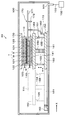
- FIG. 1 is a plan view showing an outline of a configuration of a peeling system 1 having a peeling apparatus according to the present embodiment.
- a superposed wafer T as a superposed substrate in which a target wafer W as a target substrate and a support wafer S as a support substrate are bonded with an adhesive G is used as a target wafer W. And the support wafer S is peeled off.
- a surface bonded to the support wafer S via the adhesive G is referred to as “bonding surface W J ”, and a surface opposite to the bonding surface W J is referred to as “non-bonding surface W N ”. That's it.
- the support wafer S, the surface to be bonded to the wafer W through the adhesive G is referred to as "bonding surface S J", while the opposite side of the surface as the joint surface S J "non-bonding surface S N "
- wafer W is a wafer as a product, a plurality of electronic circuits are formed, for example, joint surface W J.
- the wafer W is, for example, non-bonding surface W N is polished, thin (e.g., thickness of 50 [mu] m) it is.
- the support wafer S is a wafer having the same diameter as the wafer W to be processed and supporting the wafer W to be processed. In this embodiment, the case where a wafer is used as the support substrate will be described, but another substrate such as a glass substrate may be used.
- the peeling system 1 includes cassettes C W , C S , and C T that can accommodate, for example, a plurality of wafers W to be processed, a plurality of support wafers S, and a plurality of superposed wafers T, respectively.
- the interface station 5 that delivers the wafer W to be processed with the station 4 and the inspection apparatus 6 that inspects the wafer W before being delivered to the post-processing station 4 are integrally connected. Yes.
- the loading / unloading station 2 and the peeling treatment station 3 are arranged side by side in the X direction (vertical direction in FIG. 1).
- a wafer transfer region 7 is formed between the carry-in / out station 2 and the peeling processing station 3.
- the interface station 5 is disposed on the Y direction negative direction side (left direction side in FIG. 1) of the peeling processing station 3.
- the inspection device 6 is arranged on the positive side in the X direction of the interface station 5 (upward side in FIG. 1), and the opposite side of the inspection device 6 across the interface station 5, that is, the X of the interface station 5.
- a post-inspection cleaning apparatus 8 for cleaning the processing target wafer W after the inspection is arranged on the negative direction side.
- the loading / unloading station 2 is provided with a cassette mounting table 10.
- a plurality of, for example, three cassette mounting plates 11 are provided on the cassette mounting table 10.
- the cassette mounting plates 11 are arranged in a line in the Y direction (left and right direction in FIG. 1). These cassette mounting plates 11, cassettes C W to the outside of the peeling system 1, C S, when loading and unloading the C T, a cassette C W, C S, can be placed on C T .
- the carry-in / out station 2 is configured to be capable of holding a plurality of wafers W to be processed, a plurality of support wafers S, and a plurality of superposed wafers T.
- the number of cassette mounting plates 11 is not limited to the present embodiment, and can be arbitrarily determined. Further, the plurality of superposed wafers T carried into the carry-in / out station 2 are inspected in advance, and the superposed wafer T including the normal target wafer W and the superposed wafer T including the defective target wafer
- the first transfer device 20 is disposed in the wafer transfer region 7.
- the first transfer device 20 includes a transfer arm that can move around, for example, a vertical direction, a horizontal direction (Y direction, X direction), and a vertical axis.
- the first transfer device 20 moves in the wafer transfer region 7 and can transfer the wafer W to be processed, the support wafer S, and the overlapped wafer T between the carry-in / out station 2 and the peeling process station 3.
- the peeling processing station 3 has a peeling device 30 that peels the superposed wafer T into the processing target wafer W and the supporting wafer S.
- a first cleaning device 31 that cleans the wafer to be processed W that has been peeled off is disposed on the negative side in the Y direction of the peeling device 30 (left side in FIG. 1).
- the 2nd conveying apparatus 32 as another conveying apparatus is provided.
- a second cleaning device 33 for cleaning the peeled support wafer S is arranged on the positive side in the Y direction of the peeling device 30 (right side in FIG. 1).
- the first cleaning device 31, the second transport device 32, the peeling device 30, and the second cleaning device 33 are arranged in this order from the interface station 5 side in the peeling processing station 3.
- the inspection device 6 the presence or absence of the residue of the adhesive G on the processing target wafer W peeled by the peeling device 30 is inspected. Further, in the post-inspection cleaning apparatus 8, the wafer W to be processed in which the residue of the adhesive G is confirmed by the inspection apparatus 6 is cleaned. After the testing and cleaning device 8, the bonding surface cleaning unit 8a for cleaning the joint surface W J of wafer W, the non-bonding surface cleaning unit 8b for cleaning the non-bonding surface W N of the wafer W, the wafer W Has a reversing portion 8c for vertically reversing.
- the interface station 5 is provided with a third transfer device 41 as another transfer device that is movable on the transfer path 40 extending in the Y direction.
- the third transport device 41 is also movable in the vertical direction and the vertical axis ( ⁇ direction), and is to be processed between the peeling processing station 3, the post-processing station 4, the inspection device 6, and the post-inspection cleaning device 8.
- the wafer W can be transferred.
- predetermined post-processing is performed on the processing target wafer W peeled off at the peeling processing station 3.
- predetermined post-processing for example, processing for mounting the processing target wafer W, processing for inspecting electrical characteristics of electronic circuits on the processing target wafer W, processing for dicing the processing target wafer W for each chip, and the like are performed. .
- the peeling apparatus 30 has a housing 100 that houses a plurality of devices therein.
- a loading / unloading port (not shown) for the processing target wafer W, the support wafer S, and the overlapped wafer T is formed on the side surface of the housing 100, and an opening / closing shutter (not shown) is provided at the loading / unloading port.
- the housing 100 does not hermetically seal the inside, and is formed of, for example, a stainless steel thin plate.
- An exhaust port 101 for exhausting the inside of the casing 100 is formed on the bottom surface of the casing 100.
- An exhaust pipe 103 communicating with an exhaust device 102 such as a vacuum pump is connected to the exhaust port 101.
- a first holding unit 110 that holds the wafer W to be processed by suction on the lower surface and a second holding unit 111 that places and holds the support wafer S on the upper surface are provided.
- the first holding unit 110 is provided above the second holding unit 111 and is disposed so as to face the second holding unit 111. That is, in the housing 100, the overlapping wafer T is peeled off in a state where the processing target wafer W is disposed on the upper side and the supporting wafer S is disposed on the lower side.
- a porous chuck is used for the first holding unit 110.
- the first holding part 110 has a plate-like main body part 120.
- a porous 121 that is a porous body is provided on the lower surface side of the main body 120.
- Porous 121 has, for example, substantially the same diameter as the processed wafer W, and contact with the non-bonding surface W N of the treated wafer W.
- silicon carbide is used as the porous 121.
- a suction space 122 is formed inside the main body 120 and above the porous 121.
- the suction space 122 is formed so as to cover the porous 121, for example.
- a suction tube 123 is connected to the suction space 122.
- the suction pipe 123 is connected to a negative pressure generator (not shown) such as a vacuum pump. Then, the non-joint surface W N of the wafer to be processed is sucked from the suction pipe 123 through the suction space 122 and the porous 121, and the wafer to be processed W is sucked and held by the first holding unit 110.
- a heating mechanism 124 for heating the wafer W to be processed is provided inside the main body 120 and above the suction space 122.
- a heating mechanism 124 for example, a heater is used.
- a support plate 130 that supports the first holding unit 110 is provided on the upper surface of the first holding unit 110.
- the support plate 130 is supported on the ceiling surface of the housing 100. Note that the support plate 130 of the present embodiment may be omitted, and the first holding unit 110 may be supported in contact with the ceiling surface of the housing 100.
- a suction tube 140 for sucking and holding the support wafer S is provided inside the second holding unit 111.
- the suction tube 140 is connected to an exhaust device (not shown) such as a vacuum pump.
- a heating mechanism 141 for heating the support wafer S is provided inside the second holding unit 111.
- a heater is used for the heating mechanism 141.
- the moving mechanism 150 that moves the second holding unit 111 and the supporting wafer S in the vertical direction and the horizontal direction is provided below the second holding unit 111.
- the moving mechanism 150 includes a vertical moving unit 151 that moves the second holding unit 111 in the vertical direction and a horizontal moving unit 152 that moves the second holding unit 111 in the horizontal direction.
- the vertical moving unit 151 includes a support plate 153 that supports the lower surface of the second holding unit 111, a drive unit 154 that raises and lowers the support plate 153, and a support member 155 that supports the support plate 153.
- the drive unit 154 includes, for example, a ball screw (not shown) and a motor (not shown) that rotates the ball screw.
- the support member 155 is configured to be extendable in the vertical direction, and is provided at, for example, three locations between the support plate 153 and a support body 161 described later.
- the horizontal moving unit 152 includes a rail 160 extending along the X direction (left and right direction in FIG. 3), a support 161 attached to the rail 160, and a driving unit 162 that moves the support 161 along the rail 160.
- the drive unit 162 includes, for example, a ball screw (not shown) and a motor (not shown) that rotates the ball screw.
- the raising / lowering pin (not shown) for supporting and raising / lowering the superposition
- the elevating pin is inserted through a through hole (not shown) formed in the second holding part 111 and can protrude from the upper surface of the second holding part 111.
- an inert gas supply mechanism 170 is provided for supplying an inert gas to the bonding surface W J of the processing target wafer W.
- the inert gas supply mechanism 170 includes a flat plate-shaped porous portion 171 in which a plurality of fine holes are formed, and a gas supply pipe 172 that supplies an inert gas to the porous portion 171.
- the inert gas supply mechanism 170 is supported by the support 161 of the horizontal movement unit 152 via the support member 173. By moving the horizontal movement unit 152, the inert gas supply mechanism 170 is moved in the horizontal direction. Can be moved to.
- silicon carbide is used as the porous portion 171.
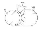
- the porous portion 171 has a flat plate shape that can cover the processing target wafer W in a plan view. Further, when the porous portion 171 is moved by the horizontal moving portion 152, a recessed portion 171 a that is recessed in a concave shape along the shape of the wafer W to be processed in a plan view is provided at the end portion in the traveling direction of the porous portion 171. Is formed. Specifically, as shown in FIG. 4, the end portion in the traveling direction of the porous portion 171 is recessed in a semicircular arc shape having substantially the same diameter as the wafer W to be processed, and the recessed portion 171a in the porous portion 171 is formed. The portion other than the size can cover the wafer W to be processed.
- the end of the porous portion 171 opposite to the end where the recess 171 a is formed has a shape protruding in a semicircular arc shape having a larger diameter than the wafer W to be processed. Accordingly, the porous portion 171 has a minimum size when covering the processing target wafer W.
- size of the porous board 171 is not limited to this Embodiment, It can set arbitrarily.
- the porous portion 171 is provided in parallel with the joint surface W J of wafer W as shown in FIG. Further, as shown in FIG. 4, the porous portion 171 is porous when the first holding portion 110 and the second holding portion 111 face each other, that is, in a state where the processing target wafer W and the support wafer S are bonded.
- the indented portion 171a of the mass portion 171 is disposed so as to be in contact with the outer peripheral portion of the processing target wafer W in plan view.
- the porous portion 171 is adjusted so as to be positioned below the joint surface W J of the processing target wafer W.
- the distance is set to 2 mm.
- a flat plate-like dispersion plate 174 is provided on the lower surface of the porous portion 171 so as to cover the porous portion 171.
- a metal plate such as aluminum or stainless steel is used.
- a gas flow path 175 is formed inside the dispersion plate 174.
- the gas supply pipe 172 is connected to the gas flow path 175 of the dispersion plate 174.
- the end of the gas supply pipe 172 opposite to the dispersion plate 174 side is connected to an inert gas supply source 176 that supplies, for example, nitrogen gas as an inert gas.
- the gas flow path 175 of the dispersion plate 174 is provided in a plurality of branches from the side where the gas supply pipe 172 is connected toward the porous portion 171, and is uniformly inert gas within the surface of the porous portion 171. It is formed so that it can be supplied. For this reason, the inert gas supplied from the inert gas supply source 176 is uniformly supplied in-plane to the porous portion 171 via the dispersion plate 174.
- the inert gas may be any gas that does not contain oxygen atoms, and is not limited to the nitrogen gas of the present embodiment.
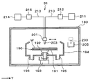
- the first cleaning device 31 has a housing 180 as shown in FIG.
- a loading / unloading port (not shown) for the wafer W to be processed is formed on the side surface of the housing 180, and an opening / closing shutter (not shown) is provided at the loading / unloading port.
- a porous chuck 190 that holds and rotates the wafer W to be processed is provided at the center of the housing 180.
- the porous chuck 190 has a flat plate-shaped main body 191 and a porous 192 provided on the upper surface side of the main body 191.
- the porous 192 has, for example, substantially the same diameter as the wafer to be processed W, and is in contact with the non-joint surface W N of the wafer to be processed W.
- the porous 192 for example, silicon carbide is used.
- a suction pipe (not shown) is connected to the porous 192, and the non-bonded surface W N of the wafer to be processed W is sucked from the suction pipe through the porous 192, so that the wafer to be processed W is placed on the porous chuck 190. Can be adsorbed and retained.
- a chuck driving unit 193 provided with a motor or the like is provided below the porous chuck 190.
- the porous chuck 190 can be rotated at a predetermined speed by the chuck driving unit 193.
- the chuck driving unit 193 is provided with an elevating drive source such as a cylinder, for example, and the porous chuck 190 is movable up and down.
- a cup 194 that receives and collects the liquid scattered or dropped from the wafer W to be processed.
- a discharge pipe 195 for discharging the collected liquid
- an exhaust pipe 196 for evacuating and exhausting the atmosphere in the cup 194.
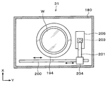
- a rail 200 extending along the Y direction is formed on the negative side of the cup 194 in the X direction (downward direction in FIG. 5).
- the rail 200 is formed, for example, from the outside of the cup 194 on the Y direction negative direction (left direction in FIG. 5) side to the outside of the Y direction positive direction (right direction in FIG. 5) side.
- An arm 201 is attached to the rail 200.
- the arm 201 supports a cleaning liquid nozzle 203 that supplies a cleaning liquid, for example, an organic solvent, to the wafer W to be processed.
- the arm 201 is movable on the rail 200 by a nozzle driving unit 204 shown in FIG.
- the cleaning liquid nozzle 203 can move from the standby unit 205 installed on the outer side of the cup 194 on the positive side in the Y direction to above the center of the wafer W to be processed in the cup 194, and further on the wafer W to be processed. Can be moved in the radial direction of the wafer W to be processed.
- the arm 201 can be moved up and down by a nozzle driving unit 204 and the height of the cleaning liquid nozzle 203 can be adjusted.
- a two-fluid nozzle is used as the cleaning liquid nozzle 203.
- a supply pipe 210 that supplies the cleaning liquid to the cleaning liquid nozzle 203 is connected to the cleaning liquid nozzle 203.
- the supply pipe 210 communicates with a cleaning liquid supply source 211 that stores the cleaning liquid therein.
- the supply pipe 210 is provided with a supply device group 212 including a valve for controlling the flow of the cleaning liquid, a flow rate adjusting unit, and the like.
- a supply pipe 213 for supplying an inert gas, for example, nitrogen gas, to the cleaning liquid nozzle 203 is connected to the cleaning liquid nozzle 203.
- the supply pipe 213 communicates with a gas supply source 214 that stores an inert gas therein.
- the supply pipe 213 is provided with a supply device group 215 including a valve for controlling the flow of the inert gas, a flow rate adjusting unit, and the like.
- the cleaning liquid and the inert gas are mixed in the cleaning liquid nozzle 203 and supplied from the cleaning liquid nozzle 203 to the wafer W to be processed.
- a mixture of a cleaning liquid and an inert gas may be simply referred to as “cleaning liquid”.
- lifting pins may be provided below the porous chuck 190 for supporting the wafer W to be processed from below and lifting it.
- the elevating pins can pass through a through hole (not shown) formed in the porous chuck 190 and protrude from the upper surface of the porous chuck 190. Then, instead of raising and lowering the porous chuck 190, the raising and lowering pins are raised and lowered, and the wafer W to be processed is transferred to and from the porous chuck 190.
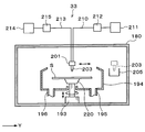
- the configuration of the second cleaning device 33 is substantially the same as the configuration of the first cleaning device 31 described above.
- the second cleaning device 33 is provided with a spin chuck 220 instead of the porous chuck 190 of the first cleaning device 31 as shown in FIG.
- the spin chuck 220 has a horizontal upper surface, and a suction port (not shown) for sucking, for example, the support wafer S is provided on the upper surface.
- the support wafer S can be sucked and held on the spin chuck 220 by suction from the suction port. Since the other structure of the 2nd washing
- cleaning apparatus 33 is the same as that of the structure of the 1st washing
- a back rinse nozzle (not shown) for injecting the cleaning liquid toward the back surface of the support wafer S, that is, the non-bonding surface SN is provided below the spin chuck 220. Also good. The non-bonding surface SN of the support wafer S and the outer peripheral portion of the support wafer S are cleaned by the cleaning liquid sprayed from the back rinse nozzle.
- the second transfer device 32 has a Bernoulli chuck 230 that holds the wafer W to be processed as shown in FIG.
- the Bernoulli chuck 230 can suspend and hold the wafer W to be processed in a non-contact state by suspending the wafer W to be processed by ejecting air.
- Bernoulli chuck 230 is supported by support arm 231.
- the support arm 231 is supported by the first drive unit 232.
- the first drive unit 232 allows the support arm 231 to rotate around the horizontal axis and extend and contract in the horizontal direction.
- a second driving unit 233 is provided below the first driving unit 232. By the second drive unit 233, the first drive unit 232 can rotate around the vertical axis and can move up and down in the vertical direction.
- the 3rd conveying apparatus 41 has the structure similar to the 2nd conveying apparatus 32 mentioned above, description is abbreviate
- the second drive unit 233 of the third transport device 41 is attached to the transport path 40 shown in FIG. 1, and the third transport device 41 is movable on the transport path 40.
- the control unit 300 is a computer, for example, and has a program storage unit (not shown).
- the program storage unit stores a program for controlling processing of the processing target wafer W, the supporting wafer S, and the overlapped wafer T in the peeling system 1.
- the program storage unit also stores a program for controlling the operation of drive systems such as the above-described various processing apparatuses and transport apparatuses to realize a peeling process described later in the peeling system 1.
- the program is recorded on a computer-readable storage medium H such as a computer-readable hard disk (HD), a flexible disk (FD), a compact disk (CD), a magnetic optical desk (MO), or a memory card. May have been installed in the control unit 300 from the storage medium H.
- FIG. 10 is a flowchart showing an example of main steps of the peeling process.
- a cassette C T accommodating a plurality of bonded wafer T, an empty cassette C W, and an empty cassette C S is placed on the predetermined cassette mounting plate 11 of the carry-out station 2.
- the superposed wafer T in the cassette CT is taken out by the first transfer device 20 and transferred to the peeling device 30 of the peeling processing station 3.
- the superposed wafer T is transported in a state where the processing target wafer W is disposed on the upper side and the support wafer S is disposed on the lower side.
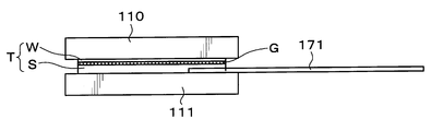
- the overlapped wafer T carried into the peeling apparatus 30 is sucked and held by the second holding unit 111. Thereafter, the second holding unit 111 is raised by the moving mechanism 150, and the overlapped wafer T is sandwiched and held between the first holding unit 110 and the second holding unit 111 as shown in FIG. At this time, the non-bonding surface W N of the wafer W is held by suction on the first holding portion 110, the non-bonding surface S N of the support wafer S is held by suction to the second holding portion 111.
- the superposed wafer T is heated to a predetermined temperature, for example, 200 ° C. by the heating mechanisms 124 and 141. Thereby, the adhesive G in the superposed wafer T is softened.
- an inert gas is supplied from the inert gas supply source 176 to the inert gas supply mechanism 170.
- the inert gas from the surface of the porous portion 171 opposite to the surface covered with the dispersion plate 174 via the gas supply pipe 172 and the dispersion plate 174, that is, the upper surface of the porous portion 171 in this embodiment. Is supplied.
- the flow rate of the inert gas supplied from the porous portion 171 is suppressed by supplying the inert gas through the porous portion 171 in which a plurality of fine holes are formed. it can. For this reason, ambient air is not involved when supplying the inert gas. Therefore, an inert gas atmosphere that does not contain air can be formed on the upper surface side of the porous portion 171 (step A1 in FIG. 10).
- the gas flow path 175 that is branched into a plurality toward the porous portion 171 is formed inside the dispersion plate 174, the inert gas is evenly distributed from the entire upper surface side of the porous portion 171. To be supplied.
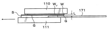
- the horizontal moving unit 152 of the moving mechanism 150 supports the second holding unit 111 and the second holding unit 111 as shown in FIG.
- the wafer S is moved in the horizontal direction.
- the inert gas supply mechanism 170 is supported by the horizontal moving unit 152 by the support 161, it moves in the horizontal direction in synchronization with the second holding unit 111 in accordance with the operation of the horizontal moving unit 152. .
- the porous portion 171 to be treated It moves in the horizontal direction without interfering with the bonding surface W J of the wafer W. Therefore, the bonding surface W J of wafer W exposed by this movement, a state of facing apart porous portion 171 and the distance L. And during this time, the bonding surface W J of wafer W inert gas is supplied from the porous portion 171.
- the second holding unit 111 is moved in the horizontal direction in a state where the supply of the inert gas from the porous portion 171 is continued, and the object to be processed held by the first holding unit 110 as shown in FIG.
- the wafer W and the support wafer S held by the second holding unit 111 are separated (step A2 in FIG. 10).
- the porous portion 171 is formed to a size capable of covering the wafer W in a plan view, continue the porous portion 171 to the bonding surface W J of wafer W that peeling is completed Inert gas is supplied.
- wafer W is lowered to a predetermined temperature, for example about 100 ° C. or less, after a state of oxidation at the joint surface W J of wafer W does not proceed, the inert gas from the porous portion 171 Supply is stopped.
- a predetermined temperature for example about 100 ° C. or less
- the wafer W to be processed peeled off by the peeling device 30 is transferred to the first cleaning device 31 by the second transfer device 32.
- the support arm 231 is extended as shown in FIG. 14, and the Bernoulli chuck 230 is held below the wafer W to be processed held by the first holding unit 110. Placed in.
- the Bernoulli chuck 230 is raised, and the suction of the wafer W to be processed from the suction tube 123 in the first holding unit 110 is stopped.
- the processing target wafer W is delivered from the first holding unit 110 to the Bernoulli chuck 230.
- the bonding surface W J of the processing target wafer W is retained on the Bernoulli chuck 230, Bernoulli chuck 230 is wafer W is held in a non-contact state. Therefore, it is possible to transport the wafer W without electronic circuitry on bonding surface W J of wafer W suffers damage.
- the support arm 231 is rotated to move the Bernoulli chuck 230 above the porous chuck 190 of the first cleaning device 31, and at the same time, the Bernoulli chuck 230 is inverted to move the wafer W to be processed. Turn downward. At this time, the porous chuck 190 is raised above the cup 194 and kept waiting. Thereafter, the wafer W to be processed is delivered from the Bernoulli chuck 230 to the porous chuck 190 and held by suction.
- the porous chuck 190 When the wafer to be processed W is sucked and held on the porous chuck 190 in this way, the porous chuck 190 is lowered to a predetermined position. Subsequently, the arm 201 moves the cleaning liquid nozzle 203 of the standby unit 205 to above the center of the wafer W to be processed. Thereafter, while rotating the wafer W by the porous chuck 190, and supplies the cleaning liquid from the cleaning liquid nozzle 203 to the bonding surface W J of wafer W. Supplied cleaning liquid is diffused over the entire surface of the bonding surface W J of wafer W by the centrifugal force, the bonding surface W J of the wafer W is cleaned (step A3 in FIG. 10).
- the plurality of superposed wafers T carried into the carry-in / out station 2 have been inspected in advance, and the superposed wafer T including the normal target wafer W and the defective target wafer W are arranged.
- the superposed wafer T is discriminated.
- the transfer of the wafer W to be processed by the third transfer device 41 is substantially the same as the transfer of the wafer W to be processed by the second transfer device 32 described above, and thus the description thereof is omitted.
- the presence or absence of adhesive residue G at the joint surface W J of wafer W is inspected (Step A4 in FIG. 10).
- the wafer W to be processed is transferred to the bonding surface cleaning unit 8a of the post-inspection cleaning device 8 by the third transfer device 41, and the bonding surface is cleaned by the bonding surface cleaning unit 8a.
- W J is cleaned (step A5 in FIG. 10).
- bonding surface W J is cleaned wafer W is transported to the inversion portion 8c by the third transporting device 41 is reversed in the vertical direction in reversing unit 8c.
- the residue of the adhesive agent G is not confirmed, the to-be-processed wafer W is reversed by the inversion part 8c, without being conveyed to the joining surface washing
- wafer W being inverted is conveyed to the inspection device 6 again by the third transporting device 41, the inspection of the non-bonding surface W N is performed (step A7 in FIG. 10).
- the wafer W to be processed is transferred to the non-bonding surface cleaning unit 8c by the third transfer device 41, and the non-bonding surface W N is cleaned. (Step A8 in FIG. 10).
- the cleaned wafer W to be processed is transferred to the post-processing station 4 by the third transfer device 41. If no residue of the adhesive G is confirmed by the inspection apparatus 6, the wafer W to be processed is transferred to the post-processing station 4 as it is without being transferred to the non-bonding surface cleaning unit 8b.
- predetermined post-processing is performed on the processing target wafer W in the post-processing station 4 (step A9 in FIG. 10).
- the processing target wafer W is commercialized.
- wafer W with a peel defects from bonded wafer T including a defect is conveyed to the station 2 loading and unloading by the first transfer device 20. Thereafter, the wafer to be processed W having a defect is unloaded from the loading / unloading station 2 and collected (step A10 in FIG. 10).
- the support wafer S peeled off by the peeling device 30 is transferred to the second cleaning device 33 by the first transfer device 20. Then, in the second cleaning device 33, bonding surface S J of the support wafer S is cleaned (step A11 in FIG. 10). Note that the cleaning of the support wafer S in the second cleaning device 33 is the same as the cleaning of the wafer W to be processed in the first cleaning device 31 described above, and thus the description thereof is omitted.
- the support wafer S which joint surface S J is cleaned is conveyed to station 2 loading and unloading by the first transfer device 20. Thereafter, the support wafer S is unloaded from the loading / unloading station 2 and collected (step A12 in FIG. 10). In this way, a series of separation processing of the processing target wafer W and the supporting wafer S is completed.
- the bonding surface W J of wafer W exposed by relatively moving the first holding portion 110 and the second holding portion 111 in a horizontal direction by a moving mechanism 150 since the inert gas is supplied from the porous portion 171 of the inert gas supply mechanism 170, a bonding surface W J of wafer W exposed by peeling can be an atmosphere of inert gas.
- a bonding surface W J of wafer W exposed by peeling can be an atmosphere of inert gas.
- the porous portion 171 of the inert gas supply mechanism 170 for a size capable of covering the wafer W, supplying an inert gas to the entire surface of the bonding surface W J of wafer W peeled can do. For this reason, oxidation can be suppressed over the entire surface of the wafer W to be processed.
- the recessed part 171a recessed in the shape of the to-be-processed wafer W in planar view is formed in the edge part of the advancing direction of the porous part 171, the porous part 171 is planarly viewed. Can be disposed at a position in contact with the wafer W to be processed. Therefore, the bonding surface W J of wafer W exposed by moving the moving mechanism 150, it is possible to supply the inert gas immediately. Specifically, when the relative movement by the moving mechanism 150 and the first holding portion 110 and the second holding portion 111 in a horizontal direction, the bonding surface W J of wafer W is crescent as shown in FIG. 16 It is exposed in a shape (range shown by hatching in FIG. 16).
- a recess 171a is formed in the porous portion 171, and the porous portion 171 is disposed so that the recess 171a contacts the wafer W to be processed in plan view, so that the entire surface of the crescent-shaped exposed portion is porous. It can be covered with a mass part 171. Therefore, it supplies an inert gas immediately on the entire surface of the exposed bonding surface W J. Note that the depression 171a is in contact with the outer peripheral portion of the wafer W to be processed in a plan view.
- the porous portion it does not mean that is, when the bonding surface W J of wafer W is exposed by the separation, without the bonding surface W J is exposed to the atmosphere of the housing 100, the porous portion This means that the recess 171a of the porous portion 171 and the outer peripheral portion of the wafer W to be processed are close to each other in plan view to the extent that it is covered with the inert gas atmosphere above 171.
- the dispersion plate 174 is provided so as to cover the porous portion 171, and the inert gas is supplied to the porous portion 171 through the dispersion plate 174, the porous portion 171 is not exposed from the entire surface opposite to the dispersion plate 174.
- the active gas can be supplied evenly. Therefore, it is possible to suppress the oxidation of the can be supplied evenly inert gas to the entire surface of the bonding surface W J of the processing the wafer W, more reliable bonding surface W J.
- the end of the porous portion 171 opposite to the end where the recess 171a is formed has a shape protruding in a semicircular arc shape having a larger diameter than the wafer to be processed W.
- the porous portion 171 can be made to have a minimum size. Thereby, the surface area of the porous part 171 can be made small, and the supply amount of the inert gas supplied from the porous part 171 can be reduced.
- silicon carbide is used as the porous portion 171, but the material of the porous portion 171 is not limited to this embodiment, and an inert gas is supplied from the porous portion 171.
- Teflon registered trademark
- Teflon or the like may be used as long as a plurality of fine holes that do not involve surrounding air are formed.
- the porous portion 171 a distance L between the joint surface W J of wafer W had a 2 mm, the distance L is long in the range of 0.5 mm ⁇ 4 mm, the processed wafer W appropriately supplying an inert gas to the bonding surface W J, it is possible to suitably suppress the progress of rapid oxidation.
- the porous portion 171 was positioned parallel to the bonding surface W J of wafer W, the porous portion 171 and the bonding surface W J of necessarily wafer W If the distance L between the porous portion 171 and the joint surface W J is maintained between 0.5 mm and 4 mm, the porous portion 171 is inclined with respect to the joint surface W J. It may be provided.
- the second holding unit 111 is moved in the horizontal direction relative to the first holding unit 110. In addition to the movement in the horizontal direction, for example, the second holding unit is moved. You may move 100 ⁇ m in the vertical direction.
- the moving distance of the second holding portion in the horizontal direction is 300 mm
- the thickness of the adhesive G in the overlapped wafer T is, for example, 30 ⁇ m to 40 ⁇ m
- the height of the electronic circuit (bump) formed on J is, for example, 20 ⁇ m. In this case, the distance between the electronic circuit on the processing target wafer W and the support wafer S is very small.
- the second holding unit 111 when the second holding unit 111 is moved only in the horizontal direction, the electronic circuit and the support wafer S may come into contact with each other and the electronic circuit may be damaged. Therefore, by moving the second holding unit 111 in the horizontal direction and also in the vertical direction, contact between the electronic circuit and the support wafer S can be avoided, and damage to the electronic circuit can be suppressed.
- the ratio of the vertical movement distance and the horizontal movement distance of the second holding unit 111 is appropriately set based on the height of the electronic circuit (bump) on the wafer W to be processed. The present invention is not limited to this embodiment.
- first holding unit 110 may be moved instead of the second holding unit. In such a case, the first holding unit 110 may be moved in the vertical direction and the horizontal direction. Alternatively, both the first holding unit 110 and the second holding unit 111 may be moved in the vertical direction and the horizontal direction.
- the inert gas supply mechanism 170 is in a horizontal direction with respect to the wafer W to be processed held by the first holding unit 110, that is, an object to which the inert gas is supplied, when moving any holding unit.
- the moving method and the supporting method can be arbitrarily set as long as they are configured to move relative to each other.
- the inert gas supply mechanism 170 may be supported on the ceiling surface of the housing 100 or may be supported on the bottom surface of the housing 100.
- the wafer W to be processed moves in the horizontal direction above the inert gas supply mechanism 170 while being separated from the inert gas supply mechanism 170 by a predetermined distance L, the exposed wafer W to be processed is exposed.
- the bonding surface W J of it can be an atmosphere of inert gas.
- the second holding unit 111 is moved only in the horizontal direction, and the moving speed of the second holding unit 111 is changed. Also good. Specifically, the moving speed at the start of moving the second holding unit 111 may be reduced, and then the moving speed may be gradually accelerated. That is, when the second holding unit 111 starts to move, the bonding area between the processing target wafer W and the support wafer S is large, and the electronic circuit on the processing target wafer W is easily affected by the adhesive G. The moving speed of the second holding unit 111 is reduced.
- the electronic circuit on the wafer to be processed W becomes less susceptible to the adhesive G, so that the moving speed of the second holding unit 111 is gradually increased. Accelerate to. Even in such a case, contact between the electronic circuit and the support wafer S can be avoided, and damage to the electronic circuit can be suppressed.
- the static electricity by peeling electrification may generate
- an inert gas ionized by an ionizer may be used as the inert gas supplied from the inert gas supply mechanism 171 in order to prevent the occurrence of peeling charging. By using the ionized inert gas, damage to the processing target wafer W due to static electricity can be prevented.
- the peeled wafer W to be processed is cleaned in the first cleaning device 31.
- the peeled support wafer S can be cleaned in the second cleaning device 33.
- a series of stripping processes from the stripping of the processing target wafer W and the supporting wafer S to the cleaning of the processing target wafer W and the cleaning of the supporting wafer S can be efficiently performed in one stripping system 1. Can be done well.
- the cleaning of the processing target wafer W and the cleaning of the support wafer S can be performed in parallel.
- the other wafer to be processed W and the support wafer S can be processed by the first cleaning device 31 and the second cleaning device 33. . Therefore, the wafer W to be processed and the support wafer S can be efficiently peeled, and the throughput of the peeling process can be improved.
- the post-processing station 5 When the wafer W to be processed peeled off at the peeling processing station 3 is a normal wafer W to be processed, the post-processing station 5 performs a predetermined post-process on the wafer W to be processed and commercializes the wafer.
- the wafer W to be processed peeled off at the peeling processing station 3 is a wafer to be processed W having a defect
- the wafer W to be processed is recovered from the loading / unloading station 2. Since only normal wafers W to be processed are commercialized in this way, the product yield can be improved. Further, the wafer to be processed W having a defect can be collected, and the wafer to be processed W can be reused depending on the degree of the defect, so that resources can be effectively utilized and the manufacturing cost can be reduced.
- the process from the separation of the wafer to be processed W and the support wafer S to the post-processing of the wafer to be processed W can be performed, so that the throughput of the wafer processing can be further improved.
- the support wafer S peeled off by the peeling device 30 is recovered from the carry-in / out station 2 after cleaning, the support wafer S can be reused. Therefore, resources can be used effectively and manufacturing costs can be reduced.
- the second transfer device 32 and the third transfer device 41 have the Bernoulli chuck 230 that holds the wafer W to be processed, even if the wafer W to be processed is thinned, the wafer W to be processed is appropriately Can be held in. Furthermore, since in the second transfer unit 32, bonding surface W J of the processing target wafer W is retained on the Bernoulli chuck 230, Bernoulli chuck 230 of the wafer W is held in a non-contact state, the electronic circuitry on bonding surface W J of wafer W will not suffer damage.
- the first cleaning device 31 includes the porous chuck 190 that holds the wafer to be processed W, the wafer to be processed can be appropriately held even if the wafer to be processed W is thinned.
- the processing target wafer W can be inspected by the inspection apparatus 6, the processing conditions in the peeling system 1 can be corrected based on the inspection result. Therefore, the processing target wafer W and the support wafer S can be more appropriately separated.
- the wafer W to be processed can be cleaned by the post-inspection cleaning apparatus 8 when an abnormality is detected in the inspection apparatus 6. Accordingly, the wafer W to be processed is not transferred to the post-processing station 4 in an abnormal state. For this reason, the fall of the yield of a product can be suppressed.
- the object to be supplied with the inert gas may be the support wafer S instead of the processing target wafer W.
- the inert gas supply mechanism 170 is provided so as to move relative to the support wafer S in the horizontal direction.
- the preferable shape and arrangement of the porous portion 171 are the same as in the case where the object to be supplied with the inert gas is the wafer W to be processed.
- the wafer to be processed W and the support wafer S are separated in a state where the wafer to be processed W is arranged on the upper side and the support wafer S is arranged on the lower side.
- the vertical arrangement of the wafer W and the support wafer S may be reversed.
- a plurality of supply ports for supplying the cleaning liquid may be formed on the surface of the Bernoulli chuck 230.
- the bonding surface W by supplying a cleaning liquid to the bonding surface W J of wafer W from the Bernoulli chuck 230
- the Bernoulli chuck 230 itself can also be cleaned. If it does so, the cleaning time of the to-be-processed wafer W in the 1st cleaning apparatus 31 after that can be shortened, and the throughput of peeling processing can further be improved.
- the Bernoulli chuck 230 can also be cleaned, the next wafer to be processed W can be appropriately transferred.
- the third transport device 41 has the Bernoulli chuck 230.
- the Bernoulli chuck 230 may have a porous chuck (not shown). Even in such a case, the wafer W to be processed thinned by the porous chuck can be appropriately sucked and held.
- the two-fluid nozzle is used as the cleaning liquid nozzle 203 of the first cleaning apparatus 31 and the second cleaning apparatus 33.
- the form of the cleaning liquid nozzle 203 is not limited to this embodiment.
- Various nozzles can be used.
- a nozzle body in which a nozzle for supplying a cleaning liquid and a nozzle for supplying an inert gas are integrated a spray nozzle, a jet nozzle, a megasonic nozzle, or the like may be used.
- a cleaning liquid heated to 80 ° C. may be supplied.
- a nozzle for supplying IPA isopropyl alcohol
- IPA isopropyl alcohol
- a temperature adjusting device for cooling the processing target wafer W heated by the peeling device 30 to a predetermined temperature may be provided.
- the temperature of the wafer W to be processed is adjusted to an appropriate temperature, so that subsequent processing can be performed more smoothly.
- the inert gas supply mechanism 170 of the peeling apparatus 30 may incorporate a heating means (not shown) for heating the inert gas, for example, a heater.
- a heating means for heating the inert gas
- the inert gas supplied to the inert gas supply mechanism 170 may be heated in advance.
- an inert gas having substantially the same temperature (for example, 200 ° C.) as that of the first holding unit 111 and the second holding unit 112 is sprayed from the inert gas supply mechanism 170 toward the processing target wafer W. That's fine.
- the superposed wafer T is not cooled by the inert gas, and the softened state of the adhesive G can be maintained. Further, since the superposed wafer T can be prevented from being cooled and contracted by the inert gas, the electronic circuit on the wafer W to be processed is not damaged.
- a monitoring unit 400 for monitoring the clogging of a plurality of holes in the porous portion 171 may be provided.
- the monitoring unit 400 includes a plurality of through holes 401 provided in the porous portion 171, a pipe 402 having one end connected to the through hole 401, and a pressure gauge 403 arranged in the middle of the pipe 402. Note that the other end of the pipe 402 is open.
- the diameter of the through hole 401 is preferably smaller, for example, 1 mm.
- the through holes 401 are provided at predetermined intervals on a line similar to the end of the recess 171a and are arranged in a plurality of rows.
- the inner surface 404 of the through hole 401 is sealed by a coating process or the like.
- a pressure gauge 403 is provided for each of the plurality of through holes 401 to detect the pressure, and when the pressure becomes lower than a predetermined value, it is considered that a clogged hole has also occurred in the porous portion 171 around the through hole 401. , Do a warning. Then, the peeling process is stopped and the porous portion 171 is cleaned. By doing so, it is possible to prevent clogging of the porous portion 171 and to always inject the inert gas from the porous portion 171 uniformly.
- the pressure difference between the room and the pressure gauge 403 is monitored, but a suction pump (not shown) may be connected to the other end of the pipe 402 and the absolute pressure may be monitored by the pressure gauge 403. .
- the monitoring unit 400 includes a block 410 and a detection unit that detects a gap between the block 410 and the porous portion 171, for example, a sensor 411. Then, during the maintenance of the peeling system 1, the block 410 is placed on the porous portion 171, and the gap between the porous portion 171 and the block 410 is measured by the sensor 411. The measurement result of the sensor 411 is output to the control unit 300. And when this measurement result is smaller than a predetermined value, it is considered that a clogged hole has occurred, and in that case, the porous portion 171 is cleaned.
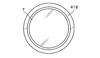
- a gas supply member 412 shown in FIGS. 20 and 21 may be further provided as an inert gas supply means.
- the gas supply member 412 is disposed at a position facing the periphery of the overlapped wafer T (support wafer S).
- the gas supply member 412 is formed in an annular shape.
- the surface 413 facing the superposed wafer T (support wafer S) is porous, and an inert gas is supplied from this surface toward the superposed wafer T (support wafer S).
- the gas supply member 412 is provided on the second holding unit 111 moved by the moving mechanism 150 and along the outer peripheral portion of the support wafer S. When the first holding unit 110 is moved by the mechanism 150, the gas supply member 412 is provided on the first holding unit 110 and along the outer peripheral portion of the wafer W to be processed.
- a plurality of holding guides 414 for holding the periphery of the wafer W to be processed may be provided on the periphery of the Bernoulli chuck 230 as shown in FIG. In this way, it is possible to prevent the position of the processing target wafer W held on the Bernoulli chuck 230 from being displaced. Further, a guide moving means 415 that moves the holding guide 414 close to and away from the processing target wafer W may be further provided.
- the post-processing station 4 performs post-processing on the wafer to be processed W to produce a product has been described. It can also be applied to the case where it is peeled off.
- the three-dimensional integration technology is a technology that meets the recent demand for higher integration of semiconductor devices. Instead of arranging a plurality of highly integrated semiconductor devices in a horizontal plane, This is a technique of three-dimensional lamination. Also in this three-dimensional integration technique, it is required to reduce the thickness of wafers to be processed, and the wafers to be processed are bonded to a support wafer to perform a predetermined process.
- the inert gas supply mechanism 170 the bonding surface W J of wafer W exposed upon separation of the bonded wafer T has been supplying the inert gas
- the inert gas supply mechanism 170 Applications are not limited to the contents of the present embodiment.
- the inert gas supply mechanism 170 is disposed so that the porous portion 171 faces the surface of the wafer to be heated without providing an airtight sealed container. Further, the progress of oxidation during the heat treatment of the wafer can be suppressed.
- the present invention is not limited to such examples. It is obvious for those skilled in the art that various modifications or modifications can be conceived within the scope of the idea described in the claims, and these naturally belong to the technical scope of the present invention. It is understood.
- the present invention is not limited to this example and can take various forms.
- the present invention can also be applied to a case where the substrate is another substrate such as an FPD (flat panel display) other than a wafer or a mask reticle for a photomask.
- FPD flat panel display
Landscapes
- Engineering & Computer Science (AREA)
- Mechanical Engineering (AREA)
- Container, Conveyance, Adherence, Positioning, Of Wafer (AREA)
Abstract
Description
ことができる。
本発明はこの例に限らず種々の態様を採りうるものである。本発明は、基板がウェハ以外のFPD(フラットパネルディスプレイ)、フォトマスク用のマスクレチクルなどの他の基板である場合にも適用できる。
2 搬入出ステーション
3 剥離処理ステーション
4 後処理ステーション
5 インターフェイスステーション
6 検査装置
7 ウェハ搬送領域
8 検査後洗浄装置
20 第1の搬送装置
30 剥離装置
31 第1の洗浄装置
32 第2の搬送装置
33 第2の洗浄装置
41 第3の搬送装置
100 筐体
101 排気口
102 排気装置
103 排気管
110 第1の保持部
111 第2の保持部
124 加熱機構
141 加熱機構
150 移動機構
151 鉛直移動部
152 水平移動部
153 支持板
154 駆動部
155 支持部材
160 レール
161 支持体
162 駆動部
170 不活性ガス供給機構
171 多孔質部
171a 窪み部
172 ガス供給管
173 支持部材
174 分散板
175 ガス流路
176 不活性ガス供給源
190 ポーラスチャック
230 ベルヌーイチャック
300 制御部
400 監視手段
412 ガス供給部材
G 接着剤
S 支持ウェハ
T 重合ウェハ
W 被処理ウェハ
L 距離
Claims (20)
- 被処理基板と支持基板が接着剤で接合された重合基板を、被処理基板と支持基板とに剥離する剥離装置であって、
被処理基板を加熱する加熱機構を備え、且つ当該被処理基板を保持する第1の保持部と、
支持基板を加熱する加熱機構を備え、且つ当該支持基板を保持する第2の保持部と、
少なくとも前記第1の保持部又は前記第2の保持部を相対的に水平方向に移動させる移動機構と、
前記移動機構により前記第1の保持部と前記第2の保持部を相対的に水平方向に移動させることで露出した被処理基板の接合面に、不活性ガスを供給する不活性ガス供給機構と、を有し、
前記不活性ガス供給機構は、複数の孔が形成された多孔質部と、前記多孔質部に接続され、当該多孔質部に不活性ガスを供給するガス供給管と、を有し、
前記多孔質部は、前記被処理基板の接合面から鉛直方向に所定の距離離間して設けられている。 - 請求項1に記載の剥離装置であって、
前記多孔質部は、平面視において前記被処理基板を覆うことができる平板形状を有する。 - 請求項1に記載の剥離装置であって、
前記多孔質部の進行方向の端部には、平面視において前記被処理基板の形状に沿って凹状に窪んだ窪み部が形成されている。 - 請求項3に記載の剥離装置であって、
前記多孔質部は、当該多孔質部の窪み部が平面視において前記被処理基板と接するように配置されている。 - 請求項1に記載の剥離装置であって、
前記移動機構は、前記第2の保持部と同期して前記多孔質部を水平方向に移動させる。 - 請求項1に記載の剥離装置であって、
前記ガス供給管は、前記多孔質部の片側の面を覆うように設けられた分散板を介して前記多孔質部と接続され、
前記分散板の内部には、前記多孔質部と前記ガス供給管に連通するガス流路が形成されている。 - 請求項1に記載の剥離装置であって、
前記多孔質部と、前記被処理基板との鉛直方向の距離は0.5mm~4mmである。 - 請求項1に記載の剥離装置であって、
前記不活性ガス供給機構から供給される不活性ガスは、イオナイザによりイオン化されたものである。 - 請求項1に記載の剥離装置であって、
前記不活性ガス供給機構は、前記被処理基板に代えて前記支持基板の接合面に不活性ガスを供給するものであり、
前記多孔質部は、前記支持基板の接合面から鉛直方向に所定の距離離間して設けられている。 - 被処理基板と支持基板が接着剤で接合された重合基板を、被処理基板と支持基板に剥離する剥離システムであって、
被処理基板、支持基板及び重合基板に所定の処理を行う剥離処理ステーションと、
前記剥離処理ステーションに対して、被処理基板、支持基板又は重合基板を搬入出する搬入出ステーションと、
前記剥離処理ステーションと前記搬入出ステーションとの間で、被処理基板、支持基板又は重合基板を搬送する搬送装置と、を有し、
前記剥離処理ステーションは、
重合基板を被処理基板と支持基板に剥離する剥離装置と、
前記剥離装置で剥離された被処理基板を洗浄する第1の洗浄装置と、
前記剥離装置で剥離された支持基板を洗浄する第2の洗浄装置と、を有し、
前記剥離装置は、
被処理基板を加熱する加熱機構を備え、且つ当該被処理基板を保持する第1の保持部と、
支持基板を加熱する加熱機構を備え、且つ当該支持基板を保持する第2の保持部と、
少なくとも前記第1の保持部又は前記第2の保持部を相対的に水平方向に移動させる移動機構と、
前記移動機構により前記第1の保持部と前記第2の保持部を相対的に水平方向に移動させることで露出した被処理基板の接合面に、不活性ガスを供給する不活性ガス供給機構と、を有し、
前記不活性ガス供給機構は、複数の孔が形成された多孔質部と、前記多孔質部に接続され、当該多孔質部に不活性ガスを供給するガス供給管と、を有し、
前記多孔質部は、前記被処理基板の接合面から鉛直方向に所定の距離離間して設けられている。 - 請求項10に記載の剥離システムであって、
前記多孔質部は、平面視において前記被処理基板を覆うことができる平板形状を有する。 - 請求項10に記載の剥離システムであって、
前記多孔質部の進行方向の端部には、平面視において前記被処理基板の形状に沿って凹状に窪んだ窪み部が形成されている。 - 請求項12に記載の剥離システムであって、
前記多孔質部は、当該多孔質部の窪み部が平面視において前記被処理基板と接するように配置されている。 - 請求項10に記載の剥離システムであって、
前記移動機構は、前記第2の保持部と同期して前記多孔質部を水平方向に移動させる。 - 請求項10に記載の剥離システムであって、
前記ガス供給管は、前記多孔質部の片側の面を覆うように設けられた分散板を介して前記多孔質部と接続され、
前記分散板の内部には、前記多孔質部と前記ガス供給管に連通するガス流路が形成されている。 - 剥離装置を用いて、被処理基板と支持基板が接着剤で接合された重合基板を、被処理基板と支持基板とに剥離する剥離方法であって、
前記剥離装置は、被処理基板を加熱する加熱機構を備え、且つ当該被処理基板を保持する第1の保持部と、支持基板を加熱する加熱機構を備え、且つ当該支持基板を保持する第2の保持部と、少なくとも前記第1の保持部又は前記第2の保持部を相対的に水平方向に移動させる移動機構と、前記被処理基板に不活性ガスを供給する不活性ガス供給機構と、を有し、
前記不活性ガス供給機構は、複数の孔が形成された多孔質部と、前記多孔質部に接続され、当該多孔質部に不活性ガスを供給するガス供給管と、を備え、
前記剥離方法は、
前記第1の保持部に保持された被処理基板と前記第2の保持部に保持された支持基板とを加熱しながら、前記第1の保持部と前記第2の保持部を相対的に水平方向に移動させて被処理基板と支持基板を剥離し、
前記多孔質部を前記被処理基板の接合面から鉛直方向に所定の距離離間させて、当該多孔質部から剥離により露出した被処理基板の接合面に不活性ガスを供給する。 - 請求項16に記載の剥離方法であって、
前記多孔質部は、平面視において前記被処理基板を覆うことができる平板形状であり、
前記多孔質部の進行方向の端部には、平面視において前記被処理基板の形状に沿って凹状に窪んだ窪み部が形成され、
さらに前記多孔質部は、当該多孔質部の窪み部が平面視において前記被処理基板と接するように配置されており、
前記不活性ガスは、少なくとも剥離により前記被処理基板の接合面が露出する以前に供給が開始される。 - 請求項17に記載の剥離方法であって、
前記不活性ガスの供給は、前記被処理基板が所定の温度以下となるまで継続される。 - 請求項16に記載の剥離方法であって、
前記不活性ガス供給機構は、剥離により露出した前記被処理基板の接合面に代えて、剥離により露出した前記支持基板の接合面に不活性ガスを供給するものであり、
前記不活性ガスの供給は、前記多孔質部を前記支持基板の接合面から鉛直方向に所定の距離離間させて行われる。 - 剥離装置を用いて、被処理基板と支持基板が接着剤で接合された重合基板を、被処理基板と支持基板とに剥離する剥離方法を剥離装置によって実行させるために、当該剥離装置を制御する制御部のコンピュータ上で動作するプログラムを格納した読み取り可能なコンピュータ記憶媒体であって、
前記剥離装置は、被処理基板を加熱する加熱機構を備え、且つ当該被処理基板を保持する第1の保持部と、支持基板を加熱する加熱機構を備え、且つ当該支持基板を保持する第2の保持部と、少なくとも前記第1の保持部又は前記第2の保持部を相対的に水平方向に移動させる移動機構と、前記被処理基板に不活性ガスを供給する不活性ガス供給機構と、を有し、
前記不活性ガス供給機構は、複数の孔が形成された多孔質部と、前記多孔質部に接続され、当該多孔質部に不活性ガスを供給するガス供給管と、を備え、
前記剥離方法は、
前記第1の保持部に保持された被処理基板と前記第2の保持部に保持された支持基板とを加熱しながら、前記第1の保持部と前記第2の保持部を相対的に水平方向に移動させて被処理基板と支持基板を剥離し、
前記多孔質部を前記被処理基板の接合面から鉛直方向に所定の距離離間させて、当該多孔質部から剥離により露出した被処理基板の接合面に不活性ガスを供給する。
Priority Applications (2)
| Application Number | Priority Date | Filing Date | Title |
|---|---|---|---|
| US13/977,134 US9919509B2 (en) | 2011-01-07 | 2011-12-16 | Peeling device, peeling system and peeling method |
| KR1020137016417A KR101837227B1 (ko) | 2011-01-07 | 2011-12-16 | 박리 장치, 박리 시스템, 박리 방법 및 컴퓨터 기억 매체 |
Applications Claiming Priority (2)
| Application Number | Priority Date | Filing Date | Title |
|---|---|---|---|
| JP2011-002560 | 2011-01-07 | ||
| JP2011002560 | 2011-01-07 |
Publications (1)
| Publication Number | Publication Date |
|---|---|
| WO2012093574A1 true WO2012093574A1 (ja) | 2012-07-12 |
Family
ID=46457434
Family Applications (1)
| Application Number | Title | Priority Date | Filing Date |
|---|---|---|---|
| PCT/JP2011/079187 Ceased WO2012093574A1 (ja) | 2011-01-07 | 2011-12-16 | 剥離装置、剥離システム、剥離方法及びコンピュータ記憶媒体 |
Country Status (5)
| Country | Link |
|---|---|
| US (1) | US9919509B2 (ja) |
| JP (1) | JP5740550B2 (ja) |
| KR (1) | KR101837227B1 (ja) |
| TW (1) | TWI523086B (ja) |
| WO (1) | WO2012093574A1 (ja) |
Cited By (2)
| Publication number | Priority date | Publication date | Assignee | Title |
|---|---|---|---|---|
| CN103579042A (zh) * | 2012-07-20 | 2014-02-12 | 台湾积体电路制造股份有限公司 | 将接合的晶圆分离的系统及方法 |
| US9324566B1 (en) | 2014-12-31 | 2016-04-26 | International Business Machines Corporation | Controlled spalling using a reactive material stack |
Families Citing this family (6)
| Publication number | Priority date | Publication date | Assignee | Title |
|---|---|---|---|---|
| JP2013033925A (ja) * | 2011-07-01 | 2013-02-14 | Tokyo Electron Ltd | 洗浄方法、プログラム、コンピュータ記憶媒体、洗浄装置及び剥離システム |
| JP5850814B2 (ja) * | 2012-09-07 | 2016-02-03 | 東京エレクトロン株式会社 | 剥離システム |
| JP6076884B2 (ja) * | 2013-11-19 | 2017-02-08 | 東京エレクトロン株式会社 | 剥離システム |
| EP3149096B1 (en) * | 2014-05-30 | 2020-06-24 | Henkel AG & Co. KGaA | A process and apparatus for detaching a display module bonded by a liquid optically clear adhesive |
| CN109144199B (zh) * | 2018-11-22 | 2020-09-01 | 武汉宁美国度科技有限公司 | 一种便于调节硬件安装位置的电脑机箱 |
| JP7146354B2 (ja) * | 2019-01-22 | 2022-10-04 | 株式会社ディスコ | キャリア板の除去方法 |
Citations (2)
| Publication number | Priority date | Publication date | Assignee | Title |
|---|---|---|---|---|
| JP2004063645A (ja) * | 2002-07-26 | 2004-02-26 | Enzan Seisakusho:Kk | 半導体ウェハの保護部材剥離装置 |
| JP2010016125A (ja) * | 2008-07-02 | 2010-01-21 | Tokyo Ohka Kogyo Co Ltd | 剥離装置および剥離方法 |
Family Cites Families (7)
| Publication number | Priority date | Publication date | Assignee | Title |
|---|---|---|---|---|
| JPH06268051A (ja) * | 1993-03-10 | 1994-09-22 | Mitsubishi Electric Corp | ウエハ剥し装置 |
| KR0165467B1 (ko) | 1995-10-31 | 1999-02-01 | 김광호 | 웨이퍼 디본더 및 이를 이용한 웨이퍼 디본딩법 |
| JP3471543B2 (ja) * | 1996-11-07 | 2003-12-02 | 大日本スクリーン製造株式会社 | 回転式基板乾燥装置 |
| DE10260233B4 (de) * | 2002-12-20 | 2016-05-19 | Infineon Technologies Ag | Verfahren zum Befestigen eines Werkstücks mit einem Feststoff an einem Werkstückträger und Werkstückträger |
| SG116533A1 (en) * | 2003-03-26 | 2005-11-28 | Toshiba Kk | Semiconductor manufacturing apparatus and method of manufacturing semiconductor device. |
| JP4090416B2 (ja) * | 2003-09-30 | 2008-05-28 | 日東電工株式会社 | 粘着テープ付ワークの離脱方法及び離脱装置 |
| JP2006135272A (ja) | 2003-12-01 | 2006-05-25 | Tokyo Ohka Kogyo Co Ltd | 基板のサポートプレート及びサポートプレートの剥離方法 |
-
2011
- 2011-12-16 WO PCT/JP2011/079187 patent/WO2012093574A1/ja not_active Ceased
- 2011-12-16 US US13/977,134 patent/US9919509B2/en active Active
- 2011-12-16 KR KR1020137016417A patent/KR101837227B1/ko active Active
- 2011-12-16 JP JP2011275502A patent/JP5740550B2/ja active Active
-
2012
- 2012-01-06 TW TW101100594A patent/TWI523086B/zh active
Patent Citations (2)
| Publication number | Priority date | Publication date | Assignee | Title |
|---|---|---|---|---|
| JP2004063645A (ja) * | 2002-07-26 | 2004-02-26 | Enzan Seisakusho:Kk | 半導体ウェハの保護部材剥離装置 |
| JP2010016125A (ja) * | 2008-07-02 | 2010-01-21 | Tokyo Ohka Kogyo Co Ltd | 剥離装置および剥離方法 |
Cited By (3)
| Publication number | Priority date | Publication date | Assignee | Title |
|---|---|---|---|---|
| CN103579042A (zh) * | 2012-07-20 | 2014-02-12 | 台湾积体电路制造股份有限公司 | 将接合的晶圆分离的系统及方法 |
| US8945344B2 (en) * | 2012-07-20 | 2015-02-03 | Taiwan Semiconductor Manufacturing Company, Ltd. | Systems and methods of separating bonded wafers |
| US9324566B1 (en) | 2014-12-31 | 2016-04-26 | International Business Machines Corporation | Controlled spalling using a reactive material stack |
Also Published As
| Publication number | Publication date |
|---|---|
| JP5740550B2 (ja) | 2015-06-24 |
| KR20130141616A (ko) | 2013-12-26 |
| JP2012156494A (ja) | 2012-08-16 |
| US20130269879A1 (en) | 2013-10-17 |
| US9919509B2 (en) | 2018-03-20 |
| TW201243922A (en) | 2012-11-01 |
| KR101837227B1 (ko) | 2018-03-09 |
| TWI523086B (zh) | 2016-02-21 |
Similar Documents
| Publication | Publication Date | Title |
|---|---|---|
| JP5740583B2 (ja) | 剥離装置、剥離システム、剥離方法、プログラム及びコンピュータ記憶媒体 | |
| JP5323867B2 (ja) | 基板反転装置、基板反転方法、剥離システム、プログラム及びコンピュータ記憶媒体 | |
| JP5740578B2 (ja) | 剥離方法、プログラム、コンピュータ記憶媒体、剥離装置及び剥離システム | |
| JP5740550B2 (ja) | 剥離装置、剥離システム、剥離方法、プログラム及びコンピュータ記憶媒体 | |
| JP5829171B2 (ja) | 剥離システム、剥離方法、プログラム及びコンピュータ記憶媒体 | |
| JP5580806B2 (ja) | 剥離装置、剥離システム、剥離方法、プログラム及びコンピュータ記憶媒体 | |
| JP5478565B2 (ja) | 接合システム | |
| JP6158721B2 (ja) | 洗浄装置、剥離システム、洗浄方法、プログラム及びコンピュータ記憶媒体 | |
| WO2012026261A1 (ja) | 剥離装置、剥離システム、剥離方法及びコンピュータ記憶媒体 | |
| JP5374462B2 (ja) | 剥離システム、剥離方法、プログラム及びコンピュータ記憶媒体 | |
| JP5314057B2 (ja) | 剥離システム、剥離方法、プログラム及びコンピュータ記憶媒体 | |
| JP5913053B2 (ja) | 剥離装置、剥離システム、剥離方法、プログラム及びコンピュータ記憶媒体 | |
| JP5777549B2 (ja) | 剥離装置、剥離システム、剥離方法、プログラム及びコンピュータ記憶媒体 | |
| WO2012176629A1 (ja) | 剥離システム、剥離方法、及びコンピュータ記憶媒体 | |
| JP5580805B2 (ja) | 剥離装置、剥離システム、剥離方法、プログラム及びコンピュータ記憶媒体 | |
| JP5717614B2 (ja) | 剥離装置、剥離システム、剥離方法、プログラム及びコンピュータ記憶媒体 | |
| JP5717803B2 (ja) | 剥離システム、剥離方法、プログラム及びコンピュータ記憶媒体 | |
| JP2013120903A (ja) | 剥離装置、剥離システム、剥離方法、プログラム及びコンピュータ記憶媒体 | |
| JP5552559B2 (ja) | 剥離システム、剥離方法、プログラム及びコンピュータ記憶媒体 | |
| JP2015207756A (ja) | 剥離装置及び剥離システム | |
| JP2015109360A (ja) | 基板保持機構及び剥離システム |
Legal Events
| Date | Code | Title | Description |
|---|---|---|---|
| 121 | Ep: the epo has been informed by wipo that ep was designated in this application |
Ref document number: 11854926 Country of ref document: EP Kind code of ref document: A1 |
|
| ENP | Entry into the national phase |
Ref document number: 20137016417 Country of ref document: KR Kind code of ref document: A |
|
| WWE | Wipo information: entry into national phase |
Ref document number: 13977134 Country of ref document: US |
|
| NENP | Non-entry into the national phase |
Ref country code: DE |
|
| 122 | Ep: pct application non-entry in european phase |
Ref document number: 11854926 Country of ref document: EP Kind code of ref document: A1 |