WO2012090879A1 - アクティブマトリクス基板 - Google Patents
アクティブマトリクス基板 Download PDFInfo
- Publication number
- WO2012090879A1 WO2012090879A1 PCT/JP2011/079917 JP2011079917W WO2012090879A1 WO 2012090879 A1 WO2012090879 A1 WO 2012090879A1 JP 2011079917 W JP2011079917 W JP 2011079917W WO 2012090879 A1 WO2012090879 A1 WO 2012090879A1
- Authority
- WO
- WIPO (PCT)
- Prior art keywords
- pixel
- auxiliary capacitance
- line
- electrode
- tft
- Prior art date
- Legal status (The legal status is an assumption and is not a legal conclusion. Google has not performed a legal analysis and makes no representation as to the accuracy of the status listed.)
- Ceased
Links
Images













Classifications
-
- G—PHYSICS
- G02—OPTICS
- G02F—OPTICAL DEVICES OR ARRANGEMENTS FOR THE CONTROL OF LIGHT BY MODIFICATION OF THE OPTICAL PROPERTIES OF THE MEDIA OF THE ELEMENTS INVOLVED THEREIN; NON-LINEAR OPTICS; FREQUENCY-CHANGING OF LIGHT; OPTICAL LOGIC ELEMENTS; OPTICAL ANALOGUE/DIGITAL CONVERTERS
- G02F1/00—Devices or arrangements for the control of the intensity, colour, phase, polarisation or direction of light arriving from an independent light source, e.g. switching, gating or modulating; Non-linear optics
- G02F1/01—Devices or arrangements for the control of the intensity, colour, phase, polarisation or direction of light arriving from an independent light source, e.g. switching, gating or modulating; Non-linear optics for the control of the intensity, phase, polarisation or colour
- G02F1/13—Devices or arrangements for the control of the intensity, colour, phase, polarisation or direction of light arriving from an independent light source, e.g. switching, gating or modulating; Non-linear optics for the control of the intensity, phase, polarisation or colour based on liquid crystals, e.g. single liquid crystal display cells
- G02F1/133—Constructional arrangements; Operation of liquid crystal cells; Circuit arrangements
- G02F1/136—Liquid crystal cells structurally associated with a semi-conducting layer or substrate, e.g. cells forming part of an integrated circuit
- G02F1/1362—Active matrix addressed cells
- G02F1/136213—Storage capacitors associated with the pixel electrode
-
- H—ELECTRICITY
- H10—SEMICONDUCTOR DEVICES; ELECTRIC SOLID-STATE DEVICES NOT OTHERWISE PROVIDED FOR
- H10B—ELECTRONIC MEMORY DEVICES
- H10B99/00—Subject matter not provided for in other groups of this subclass
- H10B99/22—Subject matter not provided for in other groups of this subclass including field-effect components
Definitions
- the present invention relates to an active matrix substrate used for a display device, an image sensor or the like.
- a display device such as a liquid crystal display device, an organic EL (Electro Luminescence) display device, a flexible display device, or an electronic book has a thin film transistor (hereinafter also referred to as “TFT”) as a switching element of each pixel.
- TFT thin film transistor
- an active matrix substrate also referred to as “TFT substrate”.
- the active matrix substrate includes a plurality of data lines, a plurality of gate lines, a plurality of TFTs disposed at intersections thereof, a pixel electrode for applying a voltage to a light modulation layer such as a liquid crystal layer, Auxiliary capacitance lines, auxiliary capacitance electrodes, and the like are formed.
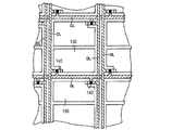
- FIG. 20 is a plan view showing a part of a plurality of pixels in the active matrix substrate disclosed in Patent Document 1.
- the active matrix substrate extends perpendicularly to the pixel electrode 130 and the TFT 140 arranged corresponding to a plurality of pixels, a plurality of gate lines (scanning lines) GL, and the plurality of gate lines GL. And a plurality of data lines (signal lines) DL.
- the liquid crystal display device of Patent Document 1 employs MFD (Multi-Field Driving) in order to increase the writing time to the pixel electrode 130 and reduce flicker.
- MFD Multi-Field Driving
- two data lines DL extend between two pixel electrodes 130 adjacent in the horizontal direction.
- the gate line GL is arranged for each of the two pixel electrodes 130. That is, the two pixel electrodes 130 extend between two gate lines GL adjacent in the vertical direction.
- the active matrix substrate is used not only as a display device but also as an image sensor substrate.
- a photodiode is arranged on an active matrix substrate so as to correspond to each pixel.
- a charge is generated by a photoelectric effect, and the generated charge is temporarily held in a plurality of pixel electrodes (or pixel capacitors).
- the held charges are sequentially read out to the signal lines by switching the ON / OFF of each TFT by an operation signal from the scanning line. In this way, the image incident on the image sensor is replaced with the image signal.
- a conversion layer that directly converts incident light into electric charge may be disposed.
- Patent Document 2 describes a liquid crystal display device and an image sensor having an active matrix substrate.
- FIG. 21 is a plan view showing a part of the active matrix substrate described in Patent Document 2.
- the active matrix substrate includes a TFT 140, a lower pixel electrode 130a, an upper pixel electrode 130b, a pixel capacitor electrode (auxiliary capacitor electrode) 410, and a plurality of gates arranged corresponding to a plurality of pixels.
- a line GL, a plurality of data lines DL, and a plurality of pixel capacitance lines (auxiliary capacitance lines) SL are provided.
- the lower layer pixel electrode 130a and the upper layer pixel electrode 130b are connected by a contact hole 720 formed in the insulating layer between both electrodes, and the lower layer pixel electrode 130a and the upper layer pixel electrode 130b function as pixel electrodes.
- the pixel capacitor line SL and the pixel capacitor electrode 410 are connected via the contact hole 400.
- a pixel capacitor (auxiliary capacitor) 140a is formed by the pixel electrode, the pixel capacitor electrode 410, and the dielectric layer between the two electrodes.
- Patent Documents 3 and 4 describe a display device, electronic paper, an electronic writing device, and the like using an electrophoresis method.
- 4 and 5 of Patent Document 3 and FIGS. 1 and 2 of Patent Document 4 describe the configuration of an active matrix substrate for such a display device and the like.
- auxiliary capacitance lines are arranged on the active matrix substrate, and auxiliary capacitance electrodes connected to the auxiliary capacitance electrodes are arranged for each pixel.
- an auxiliary capacitor counter electrode is disposed on the auxiliary capacitor electrode with an insulating layer or a dielectric layer interposed therebetween, and an auxiliary capacitor is formed by the auxiliary capacitor electrode, the insulating layer, and the auxiliary capacitor counter electrode.
- the auxiliary capacitor counter electrode is connected to the upper pixel electrode, and the potential of the pixel electrode is held for a relatively long time using the auxiliary capacitor.
- an auxiliary capacitor for holding a charge generated by photoelectric conversion for a sufficient time is formed for each pixel by the configuration described in Patent Document 2, for example.
- auxiliary capacitance lines are arranged on an active matrix substrate such as a display device or an image sensor, a large number of intersections between the auxiliary capacitance lines and the signal lines are formed, and parasitic capacitance is generated between the two lines, resulting in the SN ratio of the data signal. May occur, or the signal quality ratio may decrease due to crosstalk.
- the active matrix substrate of Patent Document 1 shown in FIG. 20 is not provided with an auxiliary capacity line, an auxiliary capacity electrode, and an auxiliary capacity counter electrode.
- This reference includes an auxiliary capacity line, an auxiliary capacity line, and an auxiliary capacity. No proposal has been made regarding the placement of the counter electrode.
- an auxiliary capacitor is formed by a pixel capacitor electrode and a pixel electrode connected to a pixel capacitor line.
- the signal lines and the pixel capacitor lines extend linearly in the vertical direction, and the scanning lines extend in the horizontal direction between any two pixels adjacent in the vertical direction. For this reason, all the signal lines and the pixel capacitance lines intersect with all the scanning lines, and signal degradation is likely to occur due to crosstalk or the like.
- FIG. 22 is a plan view showing a part of a reference example of an active matrix substrate on which auxiliary capacitance lines are arranged.
- the active matrix substrate 200 of the reference example includes a plurality of pixels 210 arranged in a matrix, a plurality of scanning lines 220, a plurality of signal lines 230 extending perpendicularly to the scanning lines 220, and the scanning lines 220.
- a plurality of auxiliary capacitance lines 240 extending in parallel are provided.
- a TFT 250, a pixel electrode 260, an auxiliary capacitance electrode 242 and an auxiliary capacitance counter electrode 262 are arranged.
- the auxiliary capacitance electrode 242 is formed of a part of the auxiliary capacitance line 240 (a portion that spreads near the center of the pixel 210).
- the storage capacitor counter electrode 262 is connected to the drain electrode of the TFT 250, and is connected to the pixel electrode 260 through a contact hole formed in an interlayer insulating layer near the center of the pixel 210.
- both the wiring and the auxiliary capacitance electrode 242 can be formed in the same layer. Therefore, it is not necessary to form a contact hole for connecting the auxiliary capacitance line 240 and the auxiliary capacitance electrode 242, and the active matrix substrate 200 can be easily manufactured.
- the signal line 230 intersects all the scanning lines 220 and the auxiliary capacitance lines 240, there is a concern that the signal quality is deteriorated.
- the present invention has been made in view of the above, and an object thereof is to provide a high-performance active matrix substrate that can secure a sufficient auxiliary capacity and can maintain high signal quality.
- An active matrix substrate includes a first scanning line and a second scanning line adjacent to each other, a plurality of scanning lines extending in the first direction, and a first signal line and a second signal line adjacent to each other.
- the auxiliary capacitance line extends in the second direction
- the first TFT is positioned on the positive side of the first direction with respect to the auxiliary capacitance line
- the second TFT is more than the auxiliary capacitance line. Located on the negative side in the first direction.
- the storage capacitor line bends and extends in the second direction
- the first storage capacitor counter electrode is positioned on the positive side in the first direction with respect to the storage capacitor line
- the second storage capacitor line is provided.
- the capacitor counter electrode is located on the negative side in the first direction with respect to the auxiliary capacitance line.
- a width of the plurality of scanning lines at a first intersection where the storage capacitor line intersects with the plurality of scanning lines is equal to the plurality of scans other than the first intersection at a boundary of the plurality of pixels. It is narrower than the line width.
- the width of the plurality of scanning lines at a second intersection where the plurality of signal lines and the plurality of scanning lines intersect is set such that the widths of the plurality of pixels other than the first intersection at the boundaries of the plurality of pixels are It is narrower than the width of the scanning line.
- the plurality of storage capacitor lines have a portion extending in the second direction and a portion extending obliquely with respect to the second direction in the first and second pixels.
- the plurality of storage capacitor lines are linearly extended in the second direction at a boundary between the first pixel and a portion extending linearly in the first direction in the first pixel. And a portion extending linearly in the first direction in the second pixel.
- a second auxiliary capacitance line connected to the auxiliary capacitance electrode and extending in the first direction is provided, and the auxiliary capacitance electrode and the second auxiliary capacitance line are formed of the same material.
- the auxiliary capacitance electrode, the first scanning line, and the second scanning line are formed of the same material in the same layer, and the first auxiliary capacitance counter electrode and the second auxiliary capacitance are formed.
- the counter electrode, the first signal line, and the second signal line are formed of the same material in the same layer.
- the auxiliary capacitance electrode, the first signal line, and the second signal line are formed of the same material in the same layer, and the first auxiliary capacitance counter electrode and the second auxiliary capacitance are formed.
- the counter electrode, the first scanning line, and the second scanning line are formed of the same material in the same layer.
- the auxiliary capacitance line extends linearly in the second direction
- the first auxiliary capacitance counter electrode is disposed on the positive side in the first direction with respect to the auxiliary capacitance line.
- a second portion disposed on the negative side of the first direction with respect to the auxiliary capacitance line, and the second auxiliary capacitance counter electrode is arranged in the first direction with respect to the auxiliary capacitance line. It is divided into a first portion arranged on the positive side and a second portion arranged on the negative side in the first direction with respect to the auxiliary capacitance line.
- the first portion of the first auxiliary capacitance counter electrode is connected to the drain electrode of the first TFT, and the first portion and the second portion of the first auxiliary capacitance counter electrode are in contact with each other.
- the second auxiliary capacitor counter electrode is connected to the first pixel electrode through a hole, the second portion of the second auxiliary capacitor counter electrode is connected to the drain electrode of the second TFT, and the second auxiliary capacitor counter electrode of the first auxiliary electrode is connected to the first pixel electrode.
- the portion and the second portion are each connected to the second pixel electrode through a contact hole.
- the first pixel electrode and the second pixel electrode are formed so as to cover the first signal line and the second signal line.
- an active matrix substrate includes a third pixel adjacent to the first pixel across the first scanning line, a fourth pixel adjacent to the second pixel across the second scanning line, and The third TFT of the third pixel connected to the first signal line, the fourth TFT of the fourth pixel connected to the second signal line, and the third TFT connected to the pixel electrode of the third pixel.
- the first TFT, the second TFT, the first auxiliary capacitance counter electrode, and the second auxiliary capacitance counter electrode are located on the positive side in the first direction with respect to the auxiliary capacitance line
- the third auxiliary capacitance counter electrode, and 4 storage capacitor counter electrodes are located on the negative side of the first direction than the storage capacitor line.
- an active matrix substrate includes a fifth pixel adjacent to the first pixel across the first signal line, a sixth pixel adjacent to the second pixel across the first signal line, The fifth TFT connected to the first scan line, the fifth TFT connected to the second scan line, the sixth TFT connected to the second scan line, and the fifth pixel connected to the pixel electrode of the fifth pixel.
- the fifth TFT and the fifth auxiliary capacitor counter electrode are located on the negative side in the first direction with respect to the other auxiliary capacitor line, and the sixth TFT And the sixth auxiliary capacitor counter electrode is provided with the other auxiliary capacitor. It is located on the positive side of the first direction than the line.
- an active matrix substrate includes a fifth pixel adjacent to the first pixel across the first signal line, a sixth pixel adjacent to the second pixel across the first signal line, The fifth TFT connected to the first signal line, the fifth TFT connected to the second signal line, the sixth TFT connected to the second signal line, and the fifth pixel connected to the pixel electrode of the fifth pixel.
- the fifth TFT, the sixth TFT, the fifth auxiliary capacitor counter electrode, and the sixth auxiliary capacitor counter electrode in the first direction with respect to the other auxiliary capacitor line. Located on the negative side of.
- the first signal line and the second signal line bend and extend in the second direction
- the auxiliary capacitance line extends linearly in the second direction
- One auxiliary capacitance counter electrode is positioned on the positive side in the first direction with respect to the auxiliary capacitance line
- the second TFT and the second auxiliary capacitance counter electrode are on the negative side in the first direction with respect to the auxiliary capacitance line. Is located.
- the first signal line, the second signal line, and the auxiliary capacitance line are bent and extended in the second direction, and the first TFT and the first auxiliary capacitance counter electrode are connected to the auxiliary capacitance line. Is located on the positive side in the first direction, and the second TFT and the second auxiliary capacitance counter electrode are located on the negative side in the first direction with respect to the auxiliary capacitance line.
- the storage capacitor line extends in the first direction
- the first TFT and the first storage capacitor counter electrode are positioned on the second direction side, which is more positive than the storage capacitor line
- the second TFT and The second auxiliary capacitance counter electrode is located on the second direction side which is more negative than the auxiliary capacitance line.
- the width of the storage capacitor line at a third intersection where the storage capacitor line and the plurality of signal lines cross each other is such that the width of the storage capacitor line other than the third intersection at the boundary of the plurality of pixels. Narrower than width.
- a width of the plurality of scanning lines at a fourth intersection where the plurality of signal lines and the plurality of scanning lines intersect is narrower than a width of the plurality of scanning lines at a boundary of the plurality of pixels.
- the width of the plurality of signal lines at the third intersection and the fourth intersection is narrower than the width of the plurality of scanning lines other than the third intersection and the fourth intersection.
- the auxiliary capacitance electrode and the auxiliary capacitance counter electrode having a large area, and thus a sufficiently large auxiliary capacitance can be obtained.
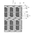
- FIG. 1 is a plan view schematically showing a configuration of an active matrix substrate 100 according to Embodiment 1 of the present invention.
- 3 is a plan view schematically showing the configuration of a display area DA in the active matrix substrate 100.
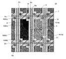
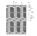
- FIG. 2 is an enlarged plan view showing a part of a display area DA in an active matrix substrate 100.
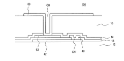
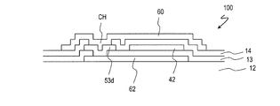
- FIG. 4 is a diagram schematically showing a configuration of a cross section a to a ′ in FIG. 3 of the active matrix substrate 100.
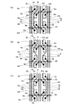
- (A) to (c) are plan views schematically showing first to third modified examples of the pixel configuration according to the first embodiment.
- (A) And (b) is the top view which represented typically the 4th and 5th modification of the pixel structure by Embodiment 1.
- FIG. 4 is a plan view schematically showing the configuration of a peripheral area PA in the active matrix substrate 100.
- FIG. FIG. 8 is a diagram schematically showing a configuration of a b-b ′ cross section in FIG. 7 of the peripheral area PA. It is the top view which represented typically the structure of the active matrix substrate 100 by Embodiment 2 of this invention. It is the top view which represented typically the structure of the active matrix substrate 100 by Embodiment 3 of this invention. It is the top view which represented typically the structure of the active matrix substrate 100 by Embodiment 4 of this invention.
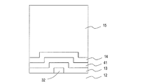
- FIG. 12 is a diagram schematically illustrating a configuration of a cross section c to c ′ in FIG. 11 of an active matrix substrate 100 according to a fourth embodiment.
- FIG. 14 is a diagram schematically showing a configuration of a d-d ′ cross section in FIG. 13 of an active matrix substrate 100 of a modified example according to the fourth embodiment.
- FIG. 10 is a plan view schematically showing the configuration of an active matrix substrate 100 according to Embodiment 5 of the present invention.
- FIG. 16 is a diagram schematically showing a configuration of an e-e ′ cross section in FIG. 15 of an active matrix substrate 100 according to a fifth embodiment.
- FIG. 16 is a diagram schematically illustrating a modification of the cross-sectional configuration along the line e to e ′ in FIG. 15.
- FIG. 10 is a plan view illustrating a configuration of a pixel in an active matrix substrate disclosed in Patent Document 2.
- FIG. It is a top view showing the composition of the pixel in the active matrix substrate of a reference example.
- An active matrix substrate according to an embodiment of the present invention is an active matrix substrate for electronic paper, display devices, electronic writing devices, liquid crystal display devices, and image sensors using an electrophoresis system, as shown in the above-mentioned patent document. Can be used.
- the active matrix substrate according to the embodiment of the present invention can also be used as an active matrix substrate for organic EL display devices, flexible displays using liquid crystal, organic EL, and the like, and X-ray sensors.
- known components may be basically used for components other than the active matrix substrate described below, such as a counter substrate and peripheral wiring.
- FIG. 1 is a plan view schematically showing a configuration of an active matrix substrate 100 according to an embodiment of the present invention.
- the active matrix substrate 100 includes a display area DA in which a plurality of pixels are arranged in a matrix and a peripheral area PA that surrounds the display area DA. Near the end of the peripheral area PA, a plurality of scanning line terminals 21, signal line terminals 31, and storage capacitor line terminals 45 are arranged.
- Each scanning line terminal 21 is connected to a scanning line (gate bus line) 20 extending in the X direction (left and right direction in the figure: first direction), and each signal line terminal 31 is connected in the Y direction (up and down direction in the figure).
- a signal line (source bus line) 30 extending in the direction (second direction) is connected, and a storage capacitor trunk line 41 extending in the X direction is connected to each storage capacitor line terminal 45.
- a plurality of storage capacitor lines (Cs lines) extend in the Y direction from each storage capacitor trunk line 41.
- peripheral area PA In the peripheral area PA, although not shown, electrical elements such as a scanning line driving circuit, a signal line driving circuit, and a voltage supply circuit are arranged in a COG (Chip on Glass) system. In addition, a terminal portion for attaching an external element such as FPC (Flexible Printed Circuits) is disposed near the outer end portion of the peripheral area PA.
- COG Chip on Glass
- FIG. 2 is a plan view showing a part of the display area DA (part A in FIG. 1) of the active matrix substrate 100.
- FIG. 3 is an enlarged plan view showing a part of FIG. .
- a plurality of pixels 10 are arranged in a matrix in the display unit DA, and a plurality of scanning lines 20 and a plurality of signal lines 30 are arranged along the boundaries of the plurality of pixels 10. However, it extends so as to be orthogonal to each other.
- Each pixel 10 includes a TFT 50 disposed in the vicinity of the corner, and a pixel electrode 60 made of, for example, ITO (Indium Tin Oxide) disposed so as to cover most of the TFT 50.
- the gate electrode, the source electrode, and the drain electrode of the TFT 50 are connected to the scanning line 20, the signal line 30, and the pixel electrode 60, respectively.
- an auxiliary capacitance line 40 that is bent and extends in the Y direction is disposed.
- Each pixel 10 is provided with an auxiliary capacitance electrode (Cs electrode) 42 connected to the auxiliary capacitance line 40 and an auxiliary capacitance counter electrode (Cs counter electrode) 62 connected to the pixel electrode 60.
- the auxiliary capacitance is formed by the auxiliary capacitance counter electrode 42 and the insulating layer or dielectric layer disposed between these electrodes.
- the signal line 30 is interrupted near the center of the display area DA, and one signal line is provided for each of the signal line 30 extending upward and the signal line 30 extending downward.
- a terminal 31 is arranged.
- 768 scanning lines and 3072 signal lines are used.
- the number of signal lines 30 is twice that number. Become.
- FIG. 4 schematically shows the configuration of the active matrix substrate 100 taken along the line a-a ′ in FIG.
- the active matrix substrate 100 includes a substrate 12 such as a glass substrate, an auxiliary capacitance electrode (Cs lower electrode) 42 formed on the substrate 12, and a substrate 12 so as to cover the auxiliary capacitance electrode 42.
- An insulating layer also referred to as a first inorganic insulating film or a gate insulating film
- An insulating layer (also referred to as a first inorganic insulating film or a gate insulating film) 13 stacked on the insulating layer 13, an auxiliary capacitance line 40 and an auxiliary capacitance counter electrode (Cs upper electrode) 62 formed on the insulating layer 13
- a layer also referred to as an organic insulating film or an interlayer insul
- a low dielectric constant material for the insulating layer 15 In order to reduce the parasitic capacitance between the pixel electrode 60 and the signal line 30, it is preferable to use a low dielectric constant material for the insulating layer 15. Therefore, it is preferable to use, for example, silicon nitride having a thickness of 0.3 ⁇ m for the insulating layer 14 and to use a photosensitive acrylic resin having a thickness of, for example, 3.0 ⁇ m and a relative dielectric constant of about 3.4 for the insulating layer 15.
- a pixel electrode 60 is formed on the insulating layer 15.
- the pixel electrode 60 is connected to the auxiliary capacitor counter electrode 62 through a contact hole CH formed in the insulating layer 15, and the auxiliary capacitor line 40 is connected to the auxiliary capacitor electrode 42 in the contact hole CH formed in the insulating layer 13. Connected through.
- the auxiliary capacitance electrode 42, the scanning line 20, and the gate electrode of the TFT 50 are obtained by patterning the metal layer in the same process, they are made of the same metal material.
- the auxiliary capacitance electrode 42, the scanning line 20, and the gate electrode of the TFT 50 have, for example, a three-layer structure of TiN / Al / Ti in which Al (aluminum) and TiN (titanium nitride) are stacked on Ti (titanium).
- the metal layer may have a multilayer structure such as Ti / Al / Ti, Al / Ti, Cu (copper) / Ti, Cu / Mo (molybdenum), or a single layer structure of one of these metals.
- the auxiliary capacitance line 40, the auxiliary capacitance counter electrode 62, the signal line 30, and the source electrode and the drain electrode of the TFT 50 are obtained by patterning the metal layer in the same process, and thus are made of the same metal material.
- the auxiliary capacitance electrode 42, the scanning line 20, and the gate electrode of the TFT 50 are made of, for example, a metal layer having a two-layer structure of Al / Ti.
- the metal layer may have a multilayer structure such as Cu / Ti, Cu / Mo, Ti / Al / Ti. Further, the above-described multilayer structure or single layer structure that can be applied to the scanning line 20 may be applied to the metal layer.
- any two scanning lines 20 adjacent to each other in the Y direction in the display area DA (the upper scanning line (first scanning line) in the figure is 20a, and the lower scanning line (second scanning line) is 20b).
- the upper scanning line (first scanning line) in the figure is 20a
- the lower scanning line (second scanning line) is 20b.
- the pixels 10a and 10b are arranged between two adjacent signal lines 30 (the right signal line (first signal line) is 30a and the left signal line (second signal line) is 30b).
- Two signal lines 30a and 30b extend between any two adjacent pixels 10 along the X direction.
- a TFT (first TFT) 50a, a pixel electrode (first pixel electrode) 60a, and a storage capacitor counter electrode (first storage capacitor counter electrode) 62a are arranged in the pixel 10a.
- a TFT ( A second TFT 50b, a pixel electrode (second pixel electrode) 60b, and a storage capacitor counter electrode (second storage capacitor counter electrode) 62b are disposed in the pixel 10b.
- the gate electrode, the source electrode, and the drain electrode of the TFT 50a are connected to the scanning line 20a, the signal line 30a, and the storage capacitor counter electrode 62a, respectively. Since the storage capacitor counter electrode 62a and the pixel electrode 60a are connected via the contact hole CH formed in the insulating layer 15, the pixel electrode 60a is electrically connected to the drain electrode of the TFT 50a.
- the gate electrode, source electrode, and drain electrode of the TFT 50b are connected to the scanning line 20b, the signal line 30b, and the storage capacitor counter electrode 62b, respectively. Since the storage capacitor counter electrode 62b and the pixel electrode 60b are connected via the contact hole CH formed in the insulating layer 15, the pixel electrode 60b is electrically connected to the drain electrode of the TFT 50b.
- the auxiliary capacitance electrode 42 disposed in the region surrounded by the scanning lines 20a and 20b and the signal lines 30a and 30b functions as auxiliary capacitance electrodes of the two pixels 10a and 10b.
- the auxiliary capacitance electrode 42 is connected to the auxiliary capacitance line 40 through a contact hole CH of the insulating layer 13 formed in the pixel 10a and a contact hole CH of the insulating layer 13 formed in the pixel 10b.
- the auxiliary capacitance electrode 42 When viewed from a direction perpendicular to the substrate surface, the auxiliary capacitance electrode 42 extends so that the auxiliary capacitance counter electrodes 62a and 62b are included therein.
- the auxiliary capacitance line 40 is bent and extended in the second direction so as to pass through the pixels 10a and 10b while avoiding the TFTs 50a and 50b. That is, the auxiliary capacitance line 40 has a portion that extends linearly in the Y direction and a portion that extends obliquely with respect to the Y direction in the pixels 10a and 10b.
- the TFT 50a and the auxiliary capacitance counter electrode 62a are located on the positive side in the X direction (right side in the figure) with respect to the auxiliary capacitance line 40, and the TFT 50b and the auxiliary capacitance counter electrode 62b are on the negative side in the X direction with respect to the auxiliary capacitance line 40. (Left side in the figure).
- two pixels adjacent in the Y direction can be scanned by one scanning line, so that the number of scanning lines is halved, and the intersection of the scanning line and the signal line. The number of decreases.
- the auxiliary capacitance line can be arranged without intersecting with the signal line, the auxiliary capacitance is ensured for each pixel and the deterioration of the signal quality is prevented.
- by bending the storage capacitor line it is possible to form a storage capacitor counter electrode having a large area with a simpler configuration, so that a large storage capacitor can be obtained with a small number of contact holes with high manufacturing efficiency.
- the data reading period or writing period (TFT selection period) can be approximately doubled as usual, so that higher quality display or data acquisition is possible. It becomes.
- the number of scanning lines can be reduced and the TFT can be reduced in size (for example, the channel length can be reduced)
- the parasitic capacitance of the TFT portion (for example, the capacitance between the gate electrode and the drain electrode) can be reduced.
- the load on the scanning line can be reduced.
- the distance between the TFT and the auxiliary capacitance electrode can be increased, and leakage defects can be reduced.
- the aperture ratio can be improved.
- the B in FIG. 3 represents an intersection (first intersection) where the auxiliary capacitance line 40 and the scanning line 20 intersect.
- the width of the scanning line 20 at the intersection B is narrower than the width of the scanning line 20 other than the intersection B at the boundary between two pixels 10 adjacent in the Y direction.
- the width of the scanning line 20 at the intersection (second intersection) C where the signal line 30 and the scanning line 20 intersect is narrower than the width of the scanning line 20 other than the intersections B and C.
- FIGS. 5A to 5C are plan views schematically showing first to third modified examples
- FIGS. 6A and 6B are schematically showing fourth and fifth modified examples.
- FIG. 6A and 6B for the sake of convenience, the direction from the right to the left in the figure is the positive X direction.
- a pixel (third pixel) adjacent to the pixel 10a across the scanning line 20a is defined as a pixel 10c, and a TFT (third TFT) and an auxiliary capacitor counter electrode (third auxiliary capacitor counter electrode) of the pixel 10c are used.
- a pixel (fourth pixel) adjacent to the pixel 10b across the scanning line 20b is defined as a pixel 10d, and a TFT (fourth TFT) and an auxiliary capacitor counter electrode (fourth auxiliary capacitor counter electrode) of the pixel 10d are respectively set to 50d and This is represented by 62d.
- a pixel (fifth pixel) 10e adjacent to the pixel 10a across the signal line 30a includes a TFT (fifth TFT) 50e and an auxiliary capacitor counter electrode (fifth auxiliary capacitor counter electrode) 62e, and the pixel 10b across the signal line 30a.
- a pixel (sixth pixel) 10f adjacent to each other includes a TFT (sixth TFT) 50f and a storage capacitor counter electrode (sixth storage capacitor counter electrode) 62f.
- an auxiliary capacitance line (another auxiliary capacitance line) extending in the second direction through the pixels 10e and 10f is referred to as an auxiliary capacitance line 40N.
- the TFT 50a and the auxiliary capacitance counter electrode 62a, and the TFT 50b and the auxiliary capacitance counter electrode 62b are located on the positive side in the X direction with respect to the auxiliary capacitance line 40.
- the TFT 50c and the auxiliary capacitor counter electrode 62c, and the TFT 50d and the auxiliary capacitor counter electrode 62d are located on the negative side in the X direction with respect to the auxiliary capacitor line 40.
- the TFT 50e and the auxiliary capacitance counter electrode 62e, and the TFT 50f and the auxiliary capacitance counter electrode 62f are located on the positive side in the X direction with respect to the auxiliary capacitance line 40N.
- the TFT 50a and the auxiliary capacitance counter electrode 62a, and the TFT 50d and the auxiliary capacitance counter electrode 62d are located on the positive side in the X direction with respect to the auxiliary capacitance line 40.
- the TFT 50b and the auxiliary capacitance counter electrode 62b, and the TFT 50c and the auxiliary capacitance counter electrode 62c are located on the negative side in the X direction with respect to the auxiliary capacitance line 40.
- the TFT 50e and the auxiliary capacitance counter electrode 62e are located on the negative side in the X direction with respect to the auxiliary capacitance line 40N, and the TFT 50f and the auxiliary capacitance counter electrode 62f are on the positive side in the X direction with respect to the auxiliary capacitance line 40N. Is located.
- the TFT 50a and the auxiliary capacitance counter electrode 62a, and the TFT 50b and the auxiliary capacitance counter electrode 62b are located on the positive side in the X direction with respect to the auxiliary capacitance line 40.
- the TFT 50c and the auxiliary capacitor counter electrode 62c, and the TFT 50d and the auxiliary capacitor counter electrode 62d are located on the negative side in the X direction with respect to the auxiliary capacitor line 40.
- the TFT 50e and the auxiliary capacitance counter electrode 62e, and the TFT 50f and the auxiliary capacitance counter electrode 62f are located on the negative side in the X direction with respect to the auxiliary capacitance line 40N.
- the signal lines 30a and 30b are bent and extend in the Y direction, and the auxiliary capacitance lines 40 and 40N extend linearly in the Y direction.
- the TFT 50a and the auxiliary capacitance counter electrode 62a, and the TFT 50d and the auxiliary capacitance counter electrode 62d are located on the positive side in the X direction from the auxiliary capacitance line 40.
- the TFT 50b and the auxiliary capacitance counter electrode 62b, and the TFT 50c and the auxiliary capacitance counter electrode are opposed to each other.
- the electrode 62c is located on the negative side in the X direction with respect to the auxiliary capacitance line 40.
- the TFT 50e and the auxiliary capacitance counter electrode 62e are located on the positive side in the X direction with respect to the auxiliary capacitance line 40N, and the TFT 50f and the auxiliary capacitance counter electrode 62f are on the negative side in the X direction with respect to the auxiliary capacitance line 40N. Is located.
- the signal lines 30a and 30b and the auxiliary capacitance lines 40 and 40N are bent and extend in the Y direction.
- the TFT 50a and the auxiliary capacitance counter electrode 62a, and the TFT 50d and the auxiliary capacitance counter electrode 62d are located on the positive side in the X direction from the auxiliary capacitance line 40.
- the TFT 50b and the auxiliary capacitance counter electrode 62b, and the TFT 50c and the auxiliary capacitance counter electrode are opposed to each other.
- the electrode 62c is located on the negative side in the X direction with respect to the auxiliary capacitance line 40.
- the TFT 50e and the auxiliary capacitance counter electrode 62e are located on the positive side in the X direction with respect to the auxiliary capacitance line 40N, and the TFT 50f and the auxiliary capacitance counter electrode 62f are on the negative side in the X direction with respect to the auxiliary capacitance line 40N. Is located.
- FIGS. 7 is a plan view schematically showing the configuration between the signal line 30 and the signal line terminal 31, and FIG. 8 is a diagram schematically showing the configuration of the bb ′ cross section in FIG. It is.
- the signal line 30 is connected to the signal line terminal 31 by a signal supply line 32 disposed in the peripheral area PA corresponding to each signal line 30.
- a plurality of auxiliary capacitance lines 40 are connected to the auxiliary capacitance main line 41.
- the signal supply line 32 is disposed below the storage capacitor main line 41 with the insulating layer 13 interposed therebetween.
- the signal line 30 and the signal supply line 32 are connected to each other via a connection portion 33 including a contact hole formed in the insulating layer 13. With such an arrangement, it is possible to prevent the signal line 30, the auxiliary capacitance line 40, and the auxiliary capacitance main line 41 arranged in the same hierarchy from being conducted.
- FIG. 9 is a cross-sectional view schematically showing the configuration of the display section DA of the active matrix substrate 100 according to the second embodiment.
- the storage capacitor line 40 includes a straight line portion extending in the Y direction in the pixels 10a and 10b and a portion extending in the X direction at the boundary between the pixel 10a and the pixel 10b.
- the auxiliary capacitance line 40 and the auxiliary capacitance electrode 42 are connected through one contact hole CH formed in the insulating layer 13 on the portion of the auxiliary capacitance line 40 extending in the X direction.
- a mode in which the auxiliary capacitance line 40 and the auxiliary capacitance electrode 42 are connected via two contact holes CH as in the first embodiment is also included in the present embodiment.
- the active matrix substrate 100 of the second embodiment since the area of the auxiliary capacitor counter electrode 62 can be increased as compared with the first embodiment, higher quality display and data acquisition are possible. Further, a contact hole connecting the auxiliary capacitance electrode 42 and the auxiliary capacitance line 40 is disposed between the pixel electrodes 60a and 60b. As a result, the risk of damaging the pixel electrode is reduced even when a contact failure or the like occurs in the contact hole, even when the melt is corrected by laser irradiation. That is, secondary defects such as leakage due to scattering of pixel electrodes can be avoided.
- FIG. 10 is a diagram schematically illustrating the configuration of the display unit DA of the active matrix substrate 100 according to the third embodiment.
- an auxiliary capacitance line (second auxiliary capacitance line) 40b extends in the X direction along the boundary between the pixel 10a and the pixel 10b.
- the auxiliary capacitance line 40b and the auxiliary capacitance electrode 42 are obtained by patterning a metal layer laminated on a substrate in one process. Therefore, the auxiliary capacitance line 40b and the auxiliary capacitance electrode 42 are formed of the same material on the same level.
- the auxiliary capacitance electrode 42 can also be considered as a part of the auxiliary capacitance line 40b extending under the pixels 10a and 10b.
- the wiring resistance of the storage capacitor line can be reduced, and the resistance distribution in the display unit can be reduced, so that display or data acquisition with higher quality can be achieved. Further, when the auxiliary capacitance electrode 42 is formed, the auxiliary capacitance electrodes 42 adjacent to each other in the X direction are interconnected, so that defects due to electrostatic charging can be reduced.
- FIG. 11 is a cross-sectional view schematically showing the configuration of the display section DA of the active matrix substrate 100 according to Embodiment 4
- FIG. 12 is a diagram schematically showing the configuration of the cc′-c ′ cross section in FIG. is there.
- the fourth embodiment has a configuration obtained by removing the auxiliary capacitance line 40 from the third embodiment, and the auxiliary capacitance electrode 42 is connected only to the auxiliary capacitance line 40b.
- the TFT 50 includes a gate electrode 51 formed on the substrate 12, a semiconductor layer 52 formed on the insulating layer 13, and each covering a part of the semiconductor layer 52. A source electrode 53s and a drain electrode 53d. The insulating layer 14 and the insulating layer 15 are laminated in this order on the source electrode 53s and the drain electrode 53d.
- auxiliary capacity electrode 42 On the auxiliary capacity electrode 42, the insulating layer 13, the auxiliary capacity counter electrode 62, the insulating layer 14, the insulating layer 15, and the pixel electrode 60 are laminated in this order.
- the drain electrode 53 d of the TFT 50 is connected to the auxiliary capacitor counter electrode 62, and the auxiliary capacitor counter electrode 62 is connected to the pixel electrode 60 through the contact hole CH formed in the insulating layers 14 and 15.
- the cross-sectional configuration of the TFT 50 shown in FIG. 12 and the auxiliary capacitance section are the same as those in the first embodiment.
- the auxiliary capacitance counter electrodes 62a and 62b are formed to be approximately the same size as the auxiliary capacitance electrode 42 except for the portions where they are close to each other. can do. Thereby, the auxiliary capacity of each pixel 10 can be increased.
- the intersection between the storage capacitor line 40 and the scanning line 20 is not formed, the quality of the scanning signal is improved.
- FIG. 13 is a cross-sectional view schematically showing the configuration of a display unit DA according to a modification of the fourth embodiment
- FIG. 14 is a diagram schematically showing the configuration of the d-d ′ cross section in FIG.
- the modified example has a configuration in which the auxiliary capacitance line 40 is removed from the third embodiment, as in the fourth embodiment, and the auxiliary capacitance electrode 42 is connected only to the auxiliary capacitance line 40b. Yes.
- the TFT 50 has the same configuration as that of the fourth embodiment.
- the auxiliary capacitance electrode 42 On the auxiliary capacitance electrode 42, the insulating layer 13, the semiconductor layer 52, the auxiliary capacitance counter electrode 62, the insulating layer 14, the insulating layer 15, and the pixel electrode 60 are laminated in this order.
- the semiconductor layer 52 is formed of the same material in the same process as the semiconductor layer 52 of the TFT 50.
- the drain electrode 53 d of the TFT 50 is connected to the auxiliary capacitor counter electrode 62, and the auxiliary capacitor counter electrode 62 penetrates the insulating layers 14 and 15 and the auxiliary capacitor counter electrode 62 and forms a contact hole CH reaching the upper portion of the semiconductor layer 52.
- To the pixel electrode 60 To the pixel electrode 60.
- FIG. 15 is a cross-sectional view schematically showing the configuration of the display section DA of the active matrix substrate 100 according to the fifth embodiment
- FIG. 16 is a diagram schematically showing the configuration of the e-e ′ cross section in FIG. is there.
- the storage capacitor line 40 extends in the Y direction substantially through the center of the pixel 10.
- the auxiliary capacitance electrode 42 is formed in the same level as the drain electrode 53 d of the TFT 50 (the same level as the source electrode, the auxiliary capacitance line 40, and the signal line 30).
- the auxiliary capacitance electrode 42 is formed of the same material at the same time in the same process as the drain electrode 53d, the source electrode, the auxiliary capacitance line 40, and the signal line 30.
- the auxiliary capacitance electrode 42 can also be considered as a part of the auxiliary capacitance line 40 extending in the pixel 10.
- the auxiliary capacitor counter electrode 62 is formed in the same level as the scanning line 20 and the gate electrode of the TFT 50.
- the storage capacitor counter electrode 62 is formed of the same material at the same time in the same process as the scanning line 20 and the gate electrode.
- the storage capacitor counter electrode 62 and the drain electrode 53d are connected to each other through a contact hole CH formed in the insulating layer 13, and the drain electrode 53d and the pixel electrode 60 are contact holes formed in the insulating layers 14 and 15. They are connected to each other via CH.
- the auxiliary capacitance in each pixel 10 is formed between the auxiliary capacitance electrode 42 and the auxiliary capacitance counter electrode 62 and between the auxiliary capacitance electrode 42 and the pixel electrode 60. Therefore, it is not necessary to form a contact hole for connecting the auxiliary capacitance line 40 and the auxiliary capacitance electrode 42, so that the manufacturing efficiency is improved.
- FIG. 17 is a cross-sectional view schematically showing the configuration of this modified example, and is a view schematically showing the configuration corresponding to the e-e ′ cross section in FIG.
- the active matrix substrate 100 basically has the same configuration as that shown in FIGS. However, as shown in FIG. 17, the insulating layer 15 is not formed, and here, a configuration in which the insulating layer 14 having the same dielectric constant as that of the insulating layer 13 is formed to the same thickness as the insulating layer 13 is shown. Yes. Therefore, according to the present embodiment, it is possible to obtain about twice as much auxiliary capacitance as compared to the case where the auxiliary capacitance electrode 42 is formed in the same layer as the scanning line 20. When it is necessary to form the insulating layer 15 in a region other than that shown in the drawing, unnecessary portions of the insulating layer 15 are removed by a photolithography method using normal exposure or halftone exposure. Also by the modification, the same effect as that of the above-described fifth embodiment can be obtained. Furthermore, when the insulating layer 15 is not formed at all, the manufacturing efficiency is improved.
- FIG. 18 is a cross-sectional view schematically showing the configuration of the display section DA of the active matrix substrate 100 according to the sixth embodiment.
- the storage capacitor line 40 extends in the Y direction substantially through the center of the pixel 10.
- the auxiliary capacitance electrode 42 is formed in the same layer as the scanning line 20 and the gate electrode of the TFT 50 as in the first embodiment, and the auxiliary capacitance counter electrode 62 is the source electrode and drain electrode of the TFT 50, the auxiliary capacitance line 40, and the signal line. 30 in the same hierarchy.
- the auxiliary capacitance line 40 extends linearly through almost the center of the pixel 10 in the Y direction.
- the storage capacitor counter electrode 62 is divided into two portions sandwiching the storage capacitor line 40 (62a-a and 62a-b in the pixel 10a, 62b-a and 62b-b in the pixel 10b).
- the auxiliary capacitance line 40 and the auxiliary capacitance electrode 42 are a contact hole formed below the auxiliary capacitance line 40 in the pixel 10a, a contact hole formed below the auxiliary capacitance line 40 in the pixel 10b, and the pixels 10a and 10b. They are connected to each other by contact holes formed at the boundary.
- the auxiliary capacitance line 40 and the auxiliary capacitance electrode 42 may be connected not by three contact holes but by one or two of these contact holes.
- the storage capacitor counter electrode 62a-a is connected to the drain electrode of the TFT 50a and to the pixel electrode 60a through a contact hole.
- the storage capacitor counter electrode 62a-b is connected to the pixel electrode 60a through a contact hole without being connected to the drain electrode of the TFT 50a.
- the storage capacitor counter electrode 62b-a is not connected to the drain electrode of the TFT 50b, but is connected to the pixel electrode 60b through a contact hole.
- the storage capacitor counter electrode 62b-b is connected to the drain electrode of the TFT 50b and to the pixel electrode 60b through a contact hole.
- FIG. 19 is a cross-sectional view schematically showing the configuration of the display section DA of the active matrix substrate 100 according to the seventh embodiment.
- the display unit DA of the seventh embodiment has basically the same configuration as that of the first embodiment.
- the pixel electrodes 10a and 10b are spread so as to cover the signal lines 30a and 30b.
- an effect of reducing light leakage in display can be obtained.
- the active matrix substrate 100 is used in a liquid crystal display device, electric field leakage from the signal lines 30a and 30b is reduced, and liquid crystal alignment abnormality due to electric field leakage can be prevented.
- the TFT 50 is replaced with two TFTs arranged in series in each pixel 10. That is, both gate electrodes of two TFTs are connected in parallel to one scanning line 20, the source electrode of one TFT is connected to the signal line 30, the drain electrode is connected to the source electrode of the other TFT, and the other The drain electrode of the TFT is connected to the auxiliary capacitor counter electrode 62 or the pixel electrode 60.
- the active matrix substrate 100 of this modification can be suitably used for a low power consumption liquid crystal display device driven at a low frequency that needs to hold a voltage for a relatively long time, electronic paper, and the like.
- Embodiments of the present invention can be suitably used for electronic paper, display devices, electronic writing devices, liquid crystal display devices, organic EL display devices, flexible displays, image sensors, X-ray sensors, and the like utilizing electrophoresis. .
- pixel 10 pixel 12 substrate 13 insulating layer (first inorganic insulating film) 14 Insulating layer (second inorganic insulating film) 15 Insulating layer (organic insulating film) 20 Scan lines (gate bus lines) 21 Scanning line terminal 30 Signal line (source bus line) 31 Signal line terminal 32 Signal supply line 33 Connection 40 Auxiliary capacitance line (Cs line) 41 Auxiliary capacity trunk wiring 42 Auxiliary capacity electrode (Cs electrode) 45 Auxiliary capacitance line terminal 50 TFT 51 Gate electrode 52 Semiconductor layer 53s Source electrode 53d Drain electrode 60 Pixel electrode 62 Auxiliary capacitor counter electrode (Cs counter electrode)
Landscapes
- Physics & Mathematics (AREA)
- Engineering & Computer Science (AREA)
- Nonlinear Science (AREA)
- Power Engineering (AREA)
- Microelectronics & Electronic Packaging (AREA)
- Mathematical Physics (AREA)
- Chemical & Material Sciences (AREA)
- Crystallography & Structural Chemistry (AREA)
- General Physics & Mathematics (AREA)
- Optics & Photonics (AREA)
- Liquid Crystal (AREA)
- Devices For Indicating Variable Information By Combining Individual Elements (AREA)
Abstract
アクティブマトリクス基板は、第1方向に延びる第1および第2走査線(20a、20b)と、第2方向に延びる第1および第2信号線(30a、30b)と、第2方向に沿って隣り合う第1および第2画素(10a、10b)と、補助容量線(40)と、第1および第2画素電極(60a、60b)と、第1TFT(50a)と、第2TFT(50b)と、補助容量線(40)に接続され、第1および第2画素電極(60a、60b)の下に広がる補助容量電極(42)と、第1画素電極(60a)に接続された第1補助容量対向電極(62a)と、第2画素電極(60b)に接続された第2補助容量対向電極(62b)と、を備えている。
Description
本発明は、表示装置、イメージセンサ等に用いられるアクティブマトリクス基板に関する。
液晶表示装置、有機EL(Electro Luminescence)表示装置、フレキシブル表示装置、電子ブック等の表示装置は、一般に、各画素のスイッチング素子として薄膜トランジスタ(Thin Film Transistor;以下、「TFT」とも呼ぶ)が形成されたアクティブマトリクス基板(「TFT基板」とも呼ぶ)を備えている。
アクティブマトリクス基板には、複数のデータラインと、複数のゲートラインと、これらの交差部にそれぞれ配置された複数のTFTと、液晶層などの光変調層に電圧を印加するための画素電極と、補助容量配線および補助容量電極などが形成されている。
アクティブマトリクス基板を用いた液晶表示装置の一例が特許文献1に記載されている。図20は、特許文献1に開示されたアクティブマトリクス基板における複数の画素の一部を表した平面図である。図20に示すように、このアクティブマトリクス基板は、複数の画素に対応して配置された画素電極130およびTFT140と、複数のゲートライン(走査線)GLと、複数のゲートラインGLに垂直に延びる複数のデータライン(信号線)DLとを備えている。
特許文献1の液晶表示装置は、画素電極130への書き込み時間を長くするとともにフリッカを低減させるために、MFD(Multi-Field Driving)が採用されている。MFDを実現するために、このアクティブマトリクス基板では、横方向に隣り合う2つの画素電極130の間に2つのデータラインDLが延びている。また、開口率を上げるために、ゲートラインGLは2つの画素電極130毎に配置されている。つまり、縦方向に沿って隣り合う2つのゲートラインGLの間に2つの画素電極130が延びている。
アクティブマトリクス基板は、表示装置のみならず、イメージセンサの基板としても用いられる。イメージセンサにおいては、各画素に対応するようにアクティブマトリクス基板上にフォトダイオードが配置されている。フォトダイオードに光が入射すると光電効果によって電荷が発生し、発生した電荷は複数の画素電極(あるいは画素容量)に一時的に保持される。保持された電荷は、走査線からの操作信号によって各TFTのON-OFFが切り換えられて、順次信号線に読み出される。このようにして、イメージセンサに入射した画像が、画像信号に置き換えられる。フォトダイオードの代わりに入射した光を直接電荷に変換する変換層を配置することも有り得る。
特許文献2には、アクティブマトリクス基板を有する液晶表示装置およびイメージセンサが記載されている。図21は、特許文献2に記載されたアクティブマトリクス基板の一部を表した平面図である。図21に示すように、このアクティブマトリクス基板は、複数の画素に対応して配置されたTFT140、下層画素電極130a、上層画素電極130b、および画素容量電極(補助容量電極)410と、複数のゲートラインGLと、複数のデータラインDLと、複数の画素容量線(補助容量線)SLを備えている。
各画素において、下層画素電極130aと上層画素電極130bは、両電極間の絶縁層に形成されたコンタクトホール720によって接続されており、下層画素電極130aおよび上層画素電極130bは画素電極として機能する。画素容量線SLと画素容量電極410は、コンタクトホール400を介して接続されている。画素電極、画素容量電極410、および両電極間の誘電体層により画素容量(補助容量)140aが形成される。
また、特許文献3および4には、電気泳動方式を利用した表示装置、電子ペーパー、電子書き込み装置等が記載されている。特許文献3の図4および図5、特許文献4の図1および図2には、そのような表示装置等のためのアクティブマトリクス基板の構成が記載されている。
表示装置によって高画質の表示を実現するためには、画素電極に与えられる電圧を、一定時間十分な値に保持させる必要がある。そのため、アクティブマトリクス基板に補助容量配線を配置するとともに、画素毎に補助容量電極に接続された補助容量電極を配置することが多い。その場合、補助容量電極の上部には、絶縁層または誘電体層を挟んで補助容量対向電極が配置され、補助容量電極、絶縁層、および補助容量対向電極によって補助容量が形成される。補助容量対向電極はその上部の画素電極に接続され、画素電極の電位が補助容量を利用して、比較的長い時間保持される。
また、イメージセンサにおいては、光電変換によって発生した電荷を十分な時間保持するための補助容量(画素容量)が、例えば上記の特許文献2に記載された構成により画素毎に形成される。
しかしながら、表示装置、イメージセンサ等のアクティブマトリクス基板に補助容量線を配置すると、補助容量線と信号線との交差部が多数形成され、両配線間に寄生容量が発生してデータ信号のSN比が低下したり、クロストークにより信号品質比が低下するといった問題が発生し得る。
図20に示した特許文献1のアクティブマトリクス基板には、補助容量線、補助容量電極、および補助容量対向電極は配置されておらず、この文献には補助容量線、補助容量線、および補助容量対向電極の配置に関する提案はなされていない。
図21に示した特許文献2のアクティブマトリクス基板には、画素容量線に接続された画素容量電極と画素電極とによって補助容量が形成されるとされている。しかし、このアクティブマトリクス基板の構成では、信号線と画素容量線が縦方向に直線的に延びるとともに、縦方向に隣り合う任意の2画素の間を走査線が横方向に延びている。そのため、全ての信号線および画素容量線は全ての走査線と交差することになり、クロストーク等により信号の劣化が生じ易い。
図22は、補助容量線を配置したアクティブマトリクス基板の参考例の一部を表した平面図である。図に示すように、参考例のアクティブマトリクス基板200は、マトリクス状に配置された複数の画素210、複数の走査線220、走査線220に垂直に延びる複数の信号線230、および走査線220に平行に延びる複数の補助容量線240を備えている。各画素210には、TFT250、画素電極260、補助容量電極242、および補助容量対向電極262が配置されている。補助容量電極242は、補助容量線240の一部(画素210の中央付近で広がった部分)からなる。補助容量対向電極262は、TFT250のドレイン電極に接続されており、また、画素210の中心付近の層間絶縁層に形成されたコンタクトホールを介して画素電極260に接続されている。
参考例のアクティブマトリクス基板200によれば、走査線220と補助容量線240とが交差しないので、両配線および補助容量電極242を同一階層に形成することができる。そのため補助容量線240と補助容量電極242とを接続するためのコンタクトホールを形成する必要がなく、アクティブマトリクス基板200の製造が容易となる。
しかし、参考例のアクティブマトリクス基板200においては、信号線230が全ての走査線220および補助容量線240と交差するため、信号品質の低下が懸念される。
本発明は、上記に鑑みてなされたものであり、十分な補助容量を確保するとともに、高い信号品質を保持し得る高性能のアクティブマトリクス基板を提供することを目的とする。
本発明の実施形態によるアクティブマトリクス基板は、隣り合う第1走査線および第2走査線を含み、第1方向に延びる複数の走査線と、隣り合う第1信号線および第2信号線を含み、第2方向に延びる複数の信号線と、前記第2方向に沿って隣り合う第1画素および第2画素を含み、マトリクス状に配置された複数の画素と、補助容量線と、前記第1走査線、前記第2走査線、前記第1信号線、および前記第2信号線に囲まれた領域に配置された前記第1画素の第1画素電極および前記第2画素の第2画素電極と、前記第1信号線に接続された前記第1画素の第1TFTと、前記第2信号線に接続された前記第2画素の第2TFTと、前記補助容量線に接続され、前記第1画素電極および前記第2画素電極の下に広がる補助容量電極と、前記第1画素電極に接続された前記第1画素の第1補助容量対向電極と、前記第2画素電極に接続された前記第2画素の第2補助容量対向電極と、を備えている。
ある実施形態では、前記補助容量線が前記第2方向に延び、前記第1TFTが前記補助容量線よりも前記第1方向の正の側に位置し、前記第2TFTが前記補助容量線よりも前記第1方向の負の側に位置している。
ある実施形態では、前記補助容量線が前記第2方向に屈曲して延び、前記第1補助容量対向電極が前記補助容量線よりも前記第1方向の正の側に位置し、前記第2補助容量対向電極が前記補助容量線よりも前記第1方向の負の側に位置している。
ある実施形態では、前記補助容量線と前記複数の走査線とが交わる第1交差部における前記複数の走査線の幅が、前記複数の画素の境界における前記第1交差部以外の前記複数の走査線の幅よりも狭い。
ある実施形態では、前記複数の信号線と前記複数の走査線とが交わる第2交差部における前記複数の走査線の幅が、前記複数の画素の境界における前記第1交差部以外の前記複数の走査線の幅よりも狭い。
ある実施形態では、前記複数の補助容量線が、前記第1および第2の画素内において、前記第2方向に延びる部分と、前記第2方向に対して斜めに延びる部分とを有する。
ある実施形態では、前記複数の補助容量線が、前記第1画素内において前記第1方向に直線的に延びる部分と、前記第1および第2の画素の境界において前記第2方向に直線的に延びる部分と、前記第2画素内において前記第1方向に直線的に延びる部分とを有する。
ある実施形態では、前記補助容量電極に接続された、前記第1の方向に延びる第2補助容量線を備え、前記補助容量電極と前記第2補助容量線とが同じ材料によって形成されている。
ある実施形態では、前記補助容量電極と前記第1走査線と前記第2走査線とが、同一の階層に同じ材料によって形成されており、前記第1補助容量対向電極と、前記第2補助容量対向電極と、前記第1信号線と、前記第2信号線とが、同一の階層に同じ材料によって形成されている。
ある実施形態では、前記補助容量電極と前記第1信号線と前記第2信号線とが、同一の階層に同じ材料によって形成されており、前記第1補助容量対向電極と、前記第2補助容量対向電極と、前記第1走査線と、前記第2走査線とが、同一の階層に同じ材料によって形成されている。
ある実施形態では、前記補助容量線が前記第2方向に直線的に延び、前記第1補助容量対向電極が、前記補助容量線よりも前記第1方向の正の側に配置された第1部分と、前記補助容量線よりも前記第1方向の負の側に配置された第2部分とに分割されており、前記第2補助容量対向電極が、前記補助容量線よりも前記第1方向の正の側に配置された第1部分と、前記補助容量線よりも前記第1方向の負の側に配置された第2部分とに分割されている。
ある実施形態では、前記第1補助容量対向電極の前記第1部分が、前記第1TFTのドレイン電極に接続され、前記第1補助容量対向電極の前記第1部分および前記第2部分が、それぞれコンタクトホールを介して前記第1画素電極に接続されており、前記第2補助容量対向電極の前記第2部分が、前記第2TFTのドレイン電極に接続され、前記第2補助容量対向電極の前記第1部分および前記第2部分が、それぞれコンタクトホールを介して前記第2画素電極に接続されている。
ある実施形態では、前記第1画素電極および第2画素電極が、前記第1信号線および前記第2信号線を覆うように形成されている。
ある実施形態では、アクティブマトリクス基板が、前記第1走査線を挟んで前記第1画素に隣り合う第3画素と、前記第2走査線を挟んで前記第2画素に隣り合う第4画素と、前記第1信号線に接続された前記第3画素の第3TFTと、前記第2信号線に接続された前記第4画素の第4TFTと、前記第3画素の画素電極に接続された前記第3画素の第3補助容量対向電極と、前記第4画素の画素電極に接続された前記第4画素の第4補助容量対向電極と、を備え、前記補助容量線が前記第2方向に延び、前記第1TFT、前記第2TFT、前記第1補助容量対向電極、および前記第2補助容量対向電極が、前記補助容量線よりも前記第1方向の正の側に位置し、前記第3TFT、前記第4TFT、前記第3補助容量対向電極、および前記第4補助容量対向電極が、前記補助容量線よりも前記第1方向の負の側に位置している。
ある実施形態では、アクティブマトリクス基板が、前記第1信号線を挟んで前記第1画素に隣り合う第5画素と、前記第1信号線を挟んで前記第2画素に隣り合う第6画素と、前記第1走査線に接続された前記第5画素の第5TFTと、前記第2走査線に接続された前記第6画素の第6TFTと、前記第5画素の画素電極に接続された前記第5画素の第5補助容量対向電極と、前記第6画素の画素電極に接続された前記第6画素の第6補助容量対向電極と、前記第5画素および前記第6画素を通って前記第2方向に延びる他の補助容量線と、を備え、前記第5TFTおよび前記第5補助容量対向電極が、前記他の補助容量線よりも前記第1方向の負の側に位置しており、前記第6TFTおよび前記第6補助容量対向電極が、前記他の補助容量線よりも前記第1方向の正の側に位置している。
ある実施形態では、アクティブマトリクス基板が、前記第1信号線を挟んで前記第1画素に隣り合う第5画素と、前記第1信号線を挟んで前記第2画素に隣り合う第6画素と、前記第1信号線に接続された前記第5画素の第5TFTと、前記第2信号線に接続された前記第6画素の第6TFTと、前記第5画素の画素電極に接続された前記第5画素の第5補助容量対向電極と、前記第6画素の画素電極に接続された前記第6画素の第6補助容量対向電極と、前記第5画素および前記第6画素を通って前記第2方向に延びる他の補助容量線と、を備え、前記第5TFT、前記第6TFT、前記第5補助容量対向電極、および前記第6補助容量対向電極が、前記他の補助容量線よりも前記第1方向の負の側に位置している。
ある実施形態では、前記第1信号線および前記第2信号線が前記第2方向に屈曲して延び、前記補助容量線が前記第2方向に直線的に延びており、前記第1TFTおよび前記第1補助容量対向電極が前記補助容量線よりも前記第1方向の正の側に位置し、前記第2TFTおよび前記第2補助容量対向電極が前記補助容量線よりも前記第1方向の負の側に位置している。
ある実施形態では、前記第1信号線、前記第2信号線、および前記補助容量線が前記第2方向に屈曲して延び、前記第1TFTおよび前記第1補助容量対向電極が前記補助容量線よりも前記第1方向の正の側に位置し、前記第2TFTおよび前記第2補助容量対向電極が前記補助容量線よりも前記第1方向の負の側に位置している。
ある実施形態では、前記補助容量線が前記第1方向に延び、前記第1TFTおよび前記第1補助容量対向電極が前記補助容量線よりも正の前記第2方向側に位置し、前記第2TFTおよび前記第2補助容量対向電極が前記補助容量線よりも負の前記第2方向側に位置している。
ある実施形態では、前記補助容量線と前記複数の信号線とが交わる第3交差部における前記補助容量線の幅が、前記複数の画素の境界における前記第3交差部以外の前記補助容量線の幅よりも狭い。
ある実施形態では、前記複数の信号線と前記複数の走査線とが交わる第4交差部における前記複数の走査線の幅が、前記複数の画素の境界における前記複数の走査線の幅よりも狭い。
ある実施形態では、前記第3交差部および前記第4交差部における前記複数の信号線の幅が、前記第3交差部および前記第4交差部以外における前記複数の走査線の幅よりも狭い。
本発明の実施形態によれば、信号線と交わる走査線および補助容量線の数が少ないため、信号データの劣化が防止され、表示装置による高品質の表示、およびイメージセンサによる高品質のデータ収集が可能となる。また、本発明の実施形態によれば、広い面積の補助容量電極および補助容量対向電極を形成することができるので、十分に大きな補助容量を得ることができる。
以下、図面を参照しながら、本発明の実施形態によるアクティブマトリクス基板を説明する。ただし、本発明の範囲は以下の実施形態に限られるものではない。
本発明の実施形態のアクティブマトリクス基板は、上記特許文献に示されたような、電気泳動方式等を利用した電子ペーパー、表示装置、電子書き込み装置、液晶表示装置、およびイメージセンサのアクティブマトリクス基板として用いられ得る。また、本発明の実施形態のアクティブマトリクス基板は、有機EL表示装置や、液晶、有機EL等を利用したフレキシブルディスプレイ、X線センサ等のアクティブマトリクス基板としても用いられ得る。本発明の実施形態によるアクティブマトリクス基板をこれら機器に用いる場合、対向基板、周辺配線など、以下に説明するアクティブマトリクス基板以外の構成要素には、基本的に公知の構成要素を用いてよい。
(実施形態1)
図1は、本発明の実施形態によるアクティブマトリクス基板100の構成を模式的に示した平面図である。
図1は、本発明の実施形態によるアクティブマトリクス基板100の構成を模式的に示した平面図である。
図1に示すように、アクティブマトリクス基板100は、複数の画素がマトリクス状に配置された表示領域DAと、表示領域DAを取り囲んで配置された周辺領域PAとを備えている。周辺領域PAの端部付近には、複数の走査線用端子21、信号線用端子31、および補助容量線用端子45が配置されている。各走査線用端子21にはX方向(図の左右方向:第1方向)に延びる走査線(ゲートバスライン)20が接続されており、各信号線用端子31にはY方向(図の上下方向:第2方向)に延びる信号線(ソースバスライン)30が接続されており、各補助容量線用端子45にはX方向に延びる補助容量幹配線41が接続されている。各補助容量幹配線41からは、複数の補助容量線(Csライン)がY方向に延びている。
周辺領域PAには、図示は省略しているが、走査線駆動回路、信号線駆動回路、電圧供給回路等の電気素子がCOG(Chip on Glass)方式で配置されている。また、周辺領域PAの外端部付近にはFPC(Flexible Printed Circuits)等の外部素子を取り付けるための端子部が配置されている。
図2は、アクティブマトリクス基板100の表示領域DAの一部(図1におけるAの部分)を表した平面図であり、図3は、図2の一部を拡大して表した平面図である。
図2および図3に示すように、表示部DAには複数の画素10がマトリックス状に配置されており、複数の画素10の境界に沿って、複数の走査線20と複数の信号線30とが、互いに直交するように延びている。各画素10は、その角部付近に配置されたTFT50、およびその大部分を覆うように配置された例えばITO(Indium Tin Oxide)からなる画素電極60を含んでいる。TFT50のゲート電極、ソース電極、およびドレイン電極は、それぞれ走査線20、信号線30、および画素電極60に接続されている。また、Y方向に延びる画素列毎に、Y方向に屈曲して延びる補助容量線40が配置されている。
各画素10には、補助容量線40に接続された補助容量電極(Cs電極)42、および画素電極60に接続された補助容量対向電極(Cs対向電極)62が配置されており、補助容量電極42、補助容量対向電極62、およびこれらの電極の間に配置された絶縁層または誘電体層によって補助容量が形成される。
図1および図2に示すように、信号線30は、表示領域DAの中央付近で途切れており、上方に延びる信号線30および下方に延びる信号線30のそれぞれに対して、1つの信号線用端子31が配置されている。例えば、図22に示した一般的な表示装置のアクティブマトリクス基板においては、768本の走査線、および3072本の信号線が用いられるが、本実施形態では信号線30の数はその2倍となる。このように信号線を配置することにより、データの読み出し期間、または書き込み期間(TFTの選択期間)を通常の約2倍とすることができ、また、信号線の1本あたりの負荷を低減できるため、より品質の高い表示またはデータ取得が可能となる。
図4は、アクティブマトリクス基板100の図3におけるa-a’断面の構成を模式的に表している。
図4に示すように、アクティブマトリクス基板100は、ガラス基板等の基板12と、基板12の上に形成された補助容量電極(Cs下部電極)42と、補助容量電極42を覆うように基板12の上に積層された絶縁層(第1無機絶縁膜またはゲート絶縁膜とも呼ぶ)13と、絶縁層13の上に形成された補助容量線40および補助容量対向電極(Cs上部電極)62と、補助容量線40および補助容量対向電極62を覆うように絶縁層13の上に積層された絶縁層(第2無機絶縁膜または保護膜とも呼ぶ)14と、絶縁層14の上に積層された絶縁層(有機絶縁膜または層間絶縁膜とも呼ぶ)15と、を有している。絶縁層13および14は、例えば、窒化シリコンまたは酸化シリコンからなる。
画素電極60と信号線30との間の寄生容量を低減させるために、絶縁層15には低誘電率の材料を用いることが好ましい。そのため絶縁層14に、例えば、厚さ0.3μmの窒化シリコンを用い、絶縁層15に、例えば、厚さ3.0μm、比誘電率3.4程度の感光性アクリル樹脂を用いることが好ましい。
絶縁層15の上には画素電極60が形成されている。画素電極60は補助容量対向電極62に、絶縁層15に形成されたコンタクトホールCHを介して接続されており、補助容量線40は補助容量電極42に、絶縁層13に形成されたコンタクトホールCHを介して接続されている。
補助容量電極42、走査線20、およびTFT50のゲート電極は、同一工程において金属層をパターニングすることによって得られるため、同一の金属材料からなる。補助容量電極42、走査線20、およびTFT50のゲート電極は、例えば、Ti(チタン)の上にAl(アルミニウム)およびTiN(窒化チタン)を積層したTiN/Al/Tiの3層構成からなる。この金属層を、Ti/Al/Ti、Al/Ti、Cu(銅)/Ti、Cu/Mo(モリブデン)等の多層構成としてもよく、これらの金属の1つによる単層構成としてもよい。
補助容量線40、補助容量対向電極62、信号線30、ならびにTFT50のソース電極およびドレイン電極は、同一工程において金属層をパターニングすることによって得られるため、同一の金属材料からなる。補助容量電極42、走査線20、およびTFT50のゲート電極は、例えば、Al/Tiの2層構成の金属層からなる。この金属層を、Cu/Ti、Cu/Mo、Ti/Al/Tiなどの多層構造としてもよい。また、この金属層に、走査線20に対して適用可能とした上述の多層構造または単層構造を適用してもよい。
次に、図2および図3を参照しながら、表示領域DAのより詳細な構成を説明する。
表示領域DAにおいてY方向に隣り合う任意の2つの走査線20(図の上側の走査線(第1走査線)を20a、下側の走査線(第2走査線)を20bとする)の間には、2つの画素10(上側の画素(第1画素)を10a、下側の画素(第2画素)を10bとする)が配置されている。画素10aおよび10bは、隣り合う2つの信号線30(右の信号線(第1信号線)を30a、左側の信号線(第2信号線)を30bとする)の間に配置されている。X方向に沿って隣り合う任意の2つの画素10の間には、2つの信号線30aおよび30bが延びている。
画素10a内には、TFT(第1TFT)50a、画素電極(第1画素電極)60a、補助容量対向電極(第1補助容量対向電極)62aが配置されており、画素10b内には、TFT(第2TFT)50b、画素電極(第2画素電極)60b、補助容量対向電極(第2補助容量対向電極)62bが配置されている。
TFT50aのゲート電極、ソース電極、およびドレイン電極は、それぞれ走査線20a、信号線30a、および補助容量対向電極62aに接続されている。補助容量対向電極62aと画素電極60aとは絶縁層15に形成されたコンタクトホールCHを介して接続されているため、画素電極60aはTFT50aのドレイン電極に電気的に接続される。TFT50bのゲート電極、ソース電極、およびドレイン電極は、それぞれ走査線20b、信号線30b、および補助容量対向電極62bに接続されている。補助容量対向電極62bと画素電極60bとは絶縁層15に形成されたコンタクトホールCHを介して接続されているため、画素電極60bはTFT50bのドレイン電極に電気的に接続される。
走査線20aおよび20bならびに信号線30aおよび30bに囲まれた領域内に配置された補助容量電極42は、2つの画素10aおよび10bの補助容量電極として機能する。補助容量電極42は画素10a内に形成された絶縁層13のコンタクトホールCH、および画素10b内に形成された絶縁層13のコンタクトホールCHを介して補助容量線40に接続されている。基板面に垂直な方向から見た場合、補助容量電極42は補助容量対向電極62aおよび62bがその内側に含まれるように広がっている。
補助容量線40は、TFT50aおよび50bを避けて画素10aおよび10bを通るように、第2方向に屈曲して延びている。つまり、補助容量線40は、画素10aおよび10bにおいて、Y方向に直線的に延びる部分と、Y方向に対して斜めに延びる部分とを有する。TFT50aおよび補助容量対向電極62aは補助容量線40よりもX方向の正の側(図中の右側)に位置し、TFT50bおよび補助容量対向電極62bは補助容量線40よりもX方向の負の側(図中の左側)に位置している。
本実施形態のアクティブマトリクス基板100によれば、1つの走査線によってY方向に隣接する2つの画素を走査することができるので、走査線の数が通常の半分となり、走査線と信号線の交差点の数が減少する。また同時に、信号線と交わることなく補助容量線を配置することができるので、画素毎に補助容量を確保するとともに、信号品質の劣化が防止される。また、補助容量線を屈曲させることにより、より簡単な構成で広い面積の補助容量対向電極を形成することができるため、少ない数のコンタクトホールにより製造効率よく大きな補助容量を得ることができる。
また、このように走査線の数が少ないため、データの読み出し期間、または書き込み期間(TFTの選択期間)を通常の約2倍とすることができるため、より品質の高い表示またはデータ取得が可能となる。また、走査線の数が減るとともにTFTを小型にすることができる(例えばチャネル長を縮小できる)ため、TFT部の寄生容量(例えばゲート電極とドレイン電極間の容量)を小さくすることができ、走査線の負荷を低減できる。また、TFTと補助容量電極等との間の距離を広く取ることができ、リーク不良を低減できる。また、透過型の液晶表示装置においては、開口率を向上することが可能となる。
図3におけるBは、補助容量線40と走査線20とが交わる交差部(第1交差部)を表している。交差部Bにおける走査線20の幅は、Y方向に隣り合う2つの画素10の境界における交差部B以外における走査線20の幅よりも狭くなっている。また、信号線30と走査線20とが交わる交差部(第2交差部)Cにおける走査線20の幅は、交差部BおよびC以外における走査線20の幅よりも狭い。このように、配線交差部における配線幅を狭くすることにより、配線の交差面積が狭まるので、配線間に生じ得る容量を低減させることができる。よって、より品質の高い信号が提供され、優れた表示およびデータ取得が可能となる。
次に、図5および図6を参照して、実施形態1による画素構成の第1~第5変形例を説明する。図5(a)~(c)は第1~第3変形例を模式的に表した平面図であり、図6(a)および(b)は第4および第5変形例を模式的に表した平面図である。なお、図6(a)および(b)においては、便宜上、図の右から左に向かう方向を正のX方向としている。
これらの変形例において、走査線20aを挟んで画素10aに隣り合う画素(第3画素)を画素10cとし、画素10cのTFT(第3TFT)および補助容量対向電極(第3補助容量対向電極)を、それぞれ50cおよび62cで表す。また、走査線20bを挟んで画素10bに隣り合う画素(第4画素)を画素10dとし、画素10dのTFT(第4TFT)および補助容量対向電極(第4補助容量対向電極)を、それぞれ50dおよび62dで表す。信号線30aを挟んで画素10aに隣り合う画素(第5画素)10eはTFT(第5TFT)50eおよび補助容量対向電極(第5補助容量対向電極)62eを含み、信号線30aを挟んで画素10bに隣り合う画素(第6画素)10fはTFT(第6TFT)50fおよび補助容量対向電極(第6補助容量対向電極)62fを含むものとする。また、画素10eおよび10fを通って前記第2方向に延びる補助容量線(他の補助容量線)を補助容量線40Nとする。
第1変形例においては、図5(a)に示すように、TFT50aおよび補助容量対向電極62a、ならびにTFT50bおよび補助容量対向電極62bは、補助容量線40よりもX方向の正の側に位置しており、TFT50cおよび補助容量対向電極62c、ならびにTFT50dおよび補助容量対向電極62dは、補助容量線40よりもX方向の負の側に位置している。また、TFT50eおよび補助容量対向電極62e、ならびにTFT50fおよび補助容量対向電極62fは、補助容量線40NよりもX方向の正の側に位置している。
第2変形例においては、図5(b)に示すように、TFT50aおよび補助容量対向電極62a、ならびにTFT50dおよび補助容量対向電極62dは、補助容量線40よりもX方向の正の側に位置しており、TFT50bおよび補助容量対向電極62b、ならびにTFT50cおよび補助容量対向電極62cは、補助容量線40よりもX方向の負の側に位置している。また、TFT50eおよび補助容量対向電極62eは、補助容量線40NよりもX方向の負の側に位置しており、TFT50fおよび補助容量対向電極62fは、補助容量線40NよりもX方向の正の側に位置している。
第3変形例においては、図5(c)に示すように、TFT50aおよび補助容量対向電極62a、ならびにTFT50bおよび補助容量対向電極62bは、補助容量線40よりもX方向の正の側に位置しており、TFT50cおよび補助容量対向電極62c、ならびにTFT50dおよび補助容量対向電極62dは、補助容量線40よりもX方向の負の側に位置している。また、TFT50eおよび補助容量対向電極62e、ならびにTFT50fおよび補助容量対向電極62fは、補助容量線40NよりもX方向の負の側に位置している。
第4変形例においては、図6(a)に示すように、信号線30aおよび30bはY方向に屈曲して延び、補助容量線40および40NはY方向に直線的に延びている。TFT50aおよび補助容量対向電極62a、ならびにTFT50dおよび補助容量対向電極62dは、補助容量線40よりもX方向の正の側に位置しており、TFT50bおよび補助容量対向電極62b、ならびにTFT50cおよび補助容量対向電極62cは、補助容量線40よりもX方向の負の側に位置している。また、TFT50eおよび補助容量対向電極62eは、補助容量線40NよりもX方向の正の側に位置しており、TFT50fおよび補助容量対向電極62fは、補助容量線40NよりもX方向の負の側に位置している。
第5変形例においては、図6(b)に示すように、信号線30aおよび30bならびに補助容量線40および40Nは、Y方向に屈曲して延びている。TFT50aおよび補助容量対向電極62a、ならびにTFT50dおよび補助容量対向電極62dは、補助容量線40よりもX方向の正の側に位置しており、TFT50bおよび補助容量対向電極62b、ならびにTFT50cおよび補助容量対向電極62cは、補助容量線40よりもX方向の負の側に位置している。また、TFT50eおよび補助容量対向電極62eは、補助容量線40NよりもX方向の正の側に位置しており、TFT50fおよび補助容量対向電極62fは、補助容量線40NよりもX方向の負の側に位置している。
次に、図7および図8を参照して、アクティブマトリクス基板100における信号線30および信号線用端子31の配置構成について説明する。図7は、信号線30と信号線用端子31との間の構成を模式的に表した平面図であり、図8は、図7におけるb~b’断面の構成を模式的に表した図である。
図7に示すように、信号線30は、各信号線30に対応して周辺領域PAに配置された信号供給線32によって信号線用端子31に接続される。補助容量幹配線41には複数の補助容量線40が接続されている。
図8に示すように、信号供給線32は、絶縁層13を挟んで補助容量幹配線41よりも下層に配置されている。信号線30と信号供給線32とは、絶縁層13に形成されたコンタクトホールを含む接続部33を介して互いに接続されている。このような配置により、同じ階層に配置されている信号線30、補助容量線40、および補助容量幹配線41が導通することが回避される。
次に、本発明による他の実施形態(実施形態2~7)を説明する。以下の説明においては、実施形態1と同じ構成要素には同じ参照番号を付け、その詳細な説明を省略する。実施形態2~7において説明する部分以外は、基本的に実施形態1と同じであり、同じ構成要素からは同様の効果を得ることができる。また、画素10aおよび画素10bを、両者を区別する必要がない場合は、画素10と表すこともある。走査線20aおよび20b、信号線30aおよび30bなど、他の一対の構成要素も同様に表すことがある。
(実施形態2)
図9は、実施形態2によるアクティブマトリクス基板100の表示部DAの構成を模式的に示す断面図である。
図9は、実施形態2によるアクティブマトリクス基板100の表示部DAの構成を模式的に示す断面図である。
図9に示すように、実施形態2においては、補助容量線40は、画素10aおよび10bの中でY方向に延びる直線部分と、画素10aと画素10bとの境界においてX方向に延びる部分とを有する。補助容量線40と補助容量電極42は、補助容量線40のX方向に延びる部分の上の絶縁層13に形成された1つのコンタクトホールCHを介して接続されている。補助容量線40と補助容量電極42を、実施形態1と同様に2つのコンタクトホールCHを介して接続した形態も、本実施形態に含まれる。
実施形態2のアクティブマトリクス基板100によれば、実施形態1に比べて補助容量対向電極62の面積を大きくすることができるので、より高品質の表示およびデータ取得が可能となる。また、補助容量電極42と補助容量線40とを接続するコンタクトホールが画素電極60aおよび60bの間に配置される。これにより、コンタクトホールにおける接続不良等が生じた場合に、レーザ照射することによってメルト修正する場合であっても、画素電極にダメージを与えるリスクが減少する。すなわち、画素電極の飛び散りによる、リーク等の二次不良を回避することができる。
(実施形態3)
図10は、実施形態3によるアクティブマトリクス基板100の表示部DAの構成を模式的に示す図である。
図10は、実施形態3によるアクティブマトリクス基板100の表示部DAの構成を模式的に示す図である。
図10に示すように、実施形態3においては、補助容量線40に加えて補助容量線(第2補助容量線)40bが、画素10aと画素10bの境界に沿ってX方向に延びている。補助容量線40bと補助容量電極42は、基板上に積層された金属層を1つの工程でパターニングして得られる。そのため、補助容量線40bと補助容量電極42は、同一階層に同一の材料によって形成されている。補助容量電極42を、画素10aおよび10bの下にまで広がった補助容量線40bの一部と考えることもできる。
この構成によれば、補助容量線の配線抵抗を小さくでき、表示部内の抵抗分布を小さくすることができるので、より品質の高い表示またはデータ取得が可能となる。また、補助容量電極42を形成した時点で、X方向に隣接する補助容量電極42が相互接続されるので、静電気の帯電による不良を低減することができる。
(実施形態4)
図11は、実施形態4によるアクティブマトリクス基板100の表示部DAの構成を模式的に示す断面図であり、図12は、図11におけるc~c’断面の構成を模式的に表した図である。
図11は、実施形態4によるアクティブマトリクス基板100の表示部DAの構成を模式的に示す断面図であり、図12は、図11におけるc~c’断面の構成を模式的に表した図である。
図11に示すように、実施形態4は実施形態3から補助容量線40を除いた構成を有しており、補助容量電極42は補助容量線40bのみに接続されている。また、図12に示すように、TFT50は、基板12の上に形成されたゲート電極51と、絶縁層13の上に形成された半導体層52と、それぞれが半導体層52の一部を覆うように形成されたソース電極53sおよびドレイン電極53dを含んでいる。ソース電極53sおよびドレイン電極53dの上には絶縁層14および絶縁層15がこの順番に積層されている。
補助容量電極42の上には、絶縁層13、補助容量対向電極62、絶縁層14、絶縁層15、および画素電極60がこの順に積層されている。TFT50のドレイン電極53dは補助容量対向電極62に接続されており、補助容量対向電極62は絶縁層14および15に形成されたコンタクトホールCHを介して画素電極60に接続されている。
図12に示したTFT50の部位および補助容量部の断面構成は、実施形態1と同じである。実施形態4では、実施形態1とは異なり、補助容量線40が形成されないため、補助容量対向電極62aおよび62bを、それぞれが近接する部分を除いて、補助容量電極42とほぼ同じ広さに形成することができる。これにより、各画素10の補助容量を増やすことができる。また、補助容量線40と走査線20との交差部が形成されないので、走査信号の品質が向上する。さらに、補助容量線40と補助容量電極42とを接続するためのコンタクトホールCHを絶縁層13に形成する必要がないので、製造効率が向上する。
次に、実施形態4の変形例を説明する。
図13は、実施形態4の変形例の表示部DAの構成を模式的に示す断面図であり、図14は、図13におけるd~d’断面の構成を模式的に表した図である。
図13に示すように、変形例は上述した実施形態4と同様、実施形態3から補助容量線40を除いた構成を有しており、補助容量電極42は補助容量線40bのみに接続されている。図14に示すように、TFT50の部位は実施形態4と同じ構成を有している。
補助容量電極42の上には、絶縁層13、半導体層52、補助容量対向電極62、絶縁層14、絶縁層15、および画素電極60がこの順に積層されている。半導体層52は、TFT50の半導体層52と同一の工程で、同じ材料によって形成されている。TFT50のドレイン電極53dは補助容量対向電極62に接続されており、補助容量対向電極62は絶縁層14および15、および補助容量対向電極62を貫通し、半導体層52の上部に達するコンタクトホールCHを介して画素電極60に接続されている。
(実施形態5)
図15は、実施形態5によるアクティブマトリクス基板100の表示部DAの構成を模式的に示す断面図であり、図16は、図15におけるe~e’断面の構成を模式的に表した図である。
図15は、実施形態5によるアクティブマトリクス基板100の表示部DAの構成を模式的に示す断面図であり、図16は、図15におけるe~e’断面の構成を模式的に表した図である。
図15に示すように、実施形態5においては、補助容量線40は画素10の概ね中心を通ってY方向に延びている。図16に示すように、補助容量電極42は、TFT50のドレイン電極53dと同じ階層(ソース電極、補助容量線40、信号線30とも同じ階層)に形成されている。補助容量電極42は、ドレイン電極53d、ソース電極、補助容量線40、および信号線30と同じ工程において、同時に同一材料によって形成される。補助容量電極42を、画素10内に広がった補助容量線40の一部と考えることもできる。
補助容量対向電極62は、走査線20およびTFT50のゲート電極と同じ階層に形成されている。補助容量対向電極62は、走査線20およびゲート電極と同じ工程において、同時に同一材料によって形成される。補助容量対向電極62とドレイン電極53dは、絶縁層13に形成されたコンタクトホールCHを介して互いに接続されており、ドレイン電極53dと画素電極60は、絶縁層14および15に形成されたコンタクトホールCHを介して互いに接続されている。
各画素10における補助容量は、補助容量電極42と補助容量対向電極62との間、および補助容量電極42と画素電極60との間で形成される。そのため、補助容量線40と補助容量電極42とを接続するためのコンタクトホールを形成する必要がないので、製造効率が向上する。
次に、実施形態5の変形例を説明する。
図17は、この変形例の構成を模式的に表した断面図であり、図15におけるe~e’断面に該当する構成を模式的に表した図である。
変形例のアクティブマトリクス基板100は、基本的に図15および図16に示したものと同じ構成を有する。ただし、図17に示すように絶縁層15は形成されず、ここには、絶縁層13と同様の比誘電率である絶縁層14を絶縁層13と同等の厚さだけ形成する構成を示している。そのため、本実施形態によれば、補助容量電極42を走査線20と同じ階層に形成する形態と比べて、約2倍の補助容量を得ることができる。絶縁層15を図に示す以外の領域に形成する必要がある場合は、通常の露光またはハーフトーン露光を用いたフォトリソグラフィ法によって、不要な部分の絶縁層15が除去される。変形例によっても、上述した実施形態5と同じ効果が得られる。さらに、絶縁層15を全く形成しない場合には、製造効率が向上する。
(実施形態6)
図18は、実施形態6によるアクティブマトリクス基板100の表示部DAの構成を模式的に示す断面図である。
図18は、実施形態6によるアクティブマトリクス基板100の表示部DAの構成を模式的に示す断面図である。
図18に示すように、実施形態6においては、補助容量線40は画素10の概ね中心を通ってY方向に延びている。補助容量電極42は、実施形態1と同様、走査線20およびTFT50のゲート電極と同じ階層に形成され、補助容量対向電極62は、TFT50のソース電極およびドレイン電極、ならびに補助容量線40、信号線30と同じ階層に形成される。
補助容量線40は、Y方向に画素10のほぼ中心を通って直線状に延びている。各画素10において、補助容量対向電極62は、補助容量線40を挟む2つの部分(画素10aにおける62a-aと62a-b、画素10bにおける62b-aと62b-b)に分割されている。補助容量線40と補助容量電極42は、画素10aにおいて補助容量線40の下部に形成されたコンタクトホール、画素10bにおいて補助容量線40の下部に形成されたコンタクトホール、および画素10aと画素10bの境界に形成されたコンタクトホールによって互いに接続されている。補助容量線40と補助容量電極42を、3つのコンタクトホールではなく、このうちの1つまたは2つのコンタクトホールで接続してもよい。
画素10aにおいて、補助容量対向電極62a-aは、TFT50aのドレイン電極に接続されるとともに、コンタクトホールによって画素電極60aに接続されている。補助容量対向電極62a-bは、TFT50aのドレイン電極に接続されることなく、コンタクトホールによって画素電極60aに接続されている。画素10bにおいて、補助容量対向電極62b-aは、TFT50bのドレイン電極に接続されることなく、コンタクトホールによって画素電極60bに接続されている。補助容量対向電極62b-bは、TFT50bのドレイン電極に接続されるとともに、コンタクトホールによって画素電極60bに接続されている。
(実施形態7)
図19は、実施形態7によるアクティブマトリクス基板100の表示部DAの構成を模式的に示す断面図である。
図19は、実施形態7によるアクティブマトリクス基板100の表示部DAの構成を模式的に示す断面図である。
図19に示すように、実施形態7の表示部DAは、基本的に実施形態1と同じ構成を有する。ただし、本実施形態においては、画素電極10aおよび10bが、信号線30aおよび30bを覆うように広がっている。これにより、実施形態1から得られる利点に加えて、表示における光漏れを減少させるという効果が得られる。また、アクティブマトリクス基板100を液晶表示装置に用いる場合、信号線30aおよび30bからの電界漏れが低減され、電界漏れに起因する液晶の配向異常を防止することができる。
本実施形態の変形例として、各画素10においてTFT50を直列に配置した2つのTFTに置き換えた形態がある。つまり、2つのTFTの両方のゲート電極を1つの走査線20に平行接続し、一方のTFTのソース電極を信号線30に接続し、そのドレイン電極を他方のTFTのソース電極に接続し、他方のTFTのドレイン電極を補助容量対向電極62または画素電極60に接続する形態である。
この変形例によれば、TFTの非選択期間に発生するリーク電流を低減させることができる。したがって、この変形例のアクティブマトリクス基板100は、比較的長い時間電圧を保持する必要のある低周波で駆動する低消費電力の液晶表示装置や、電子ペーパーなどに好適に用いられ得る。
本発明の実施形態は、電気泳動方式等を利用した電子ペーパー、表示装置、および電子書き込み装置、液晶表示装置、有機EL表示装置、フレキシブルディスプレイ、イメージセンサ、X線センサ等に好適に用いられ得る。
10 画素
12 基板
13 絶縁層(第1無機絶縁膜)
14 絶縁層(第2無機絶縁膜)
15 絶縁層(有機絶縁膜)
20 走査線(ゲートバスライン)
21 走査線用端子
30 信号線(ソースバスライン)
31 信号線用端子
32 信号供給線
33 接続部
40 補助容量線(Csライン)
41 補助容量幹配線
42 補助容量電極(Cs電極)
45 補助容量線用端子
50 TFT
51 ゲート電極
52 半導体層
53s ソース電極
53d ドレイン電極
60 画素電極
62 補助容量対向電極(Cs対向電極)
12 基板
13 絶縁層(第1無機絶縁膜)
14 絶縁層(第2無機絶縁膜)
15 絶縁層(有機絶縁膜)
20 走査線(ゲートバスライン)
21 走査線用端子
30 信号線(ソースバスライン)
31 信号線用端子
32 信号供給線
33 接続部
40 補助容量線(Csライン)
41 補助容量幹配線
42 補助容量電極(Cs電極)
45 補助容量線用端子
50 TFT
51 ゲート電極
52 半導体層
53s ソース電極
53d ドレイン電極
60 画素電極
62 補助容量対向電極(Cs対向電極)
Claims (22)
- 隣り合う第1走査線および第2走査線を含み、第1方向に延びる複数の走査線と、
隣り合う第1信号線および第2信号線を含み、第2方向に延びる複数の信号線と、
前記第2方向に沿って隣り合う第1画素および第2画素を含み、マトリクス状に配置された複数の画素と、
補助容量線と、
前記第1走査線、前記第2走査線、前記第1信号線、および前記第2信号線に囲まれた領域に配置された前記第1画素の第1画素電極および前記第2画素の第2画素電極と、
前記第1信号線に接続された前記第1画素の第1TFTと、
前記第2信号線に接続された前記第2画素の第2TFTと、
前記補助容量線に接続され、前記第1画素電極および前記第2画素電極の下に広がる補助容量電極と、
前記第1画素電極に接続された前記第1画素の第1補助容量対向電極と、
前記第2画素電極に接続された前記第2画素の第2補助容量対向電極と、を備えたアクティブマトリクス基板。 - 前記補助容量線が前記第2方向に延び、
前記第1TFTが前記補助容量線よりも前記第1方向の正の側に位置し、
前記第2TFTが前記補助容量線よりも前記第1方向の負の側に位置している、請求項1に記載のアクティブマトリクス基板。 - 前記補助容量線が前記第2方向に屈曲して延び、
前記第1補助容量対向電極が前記補助容量線よりも前記第1方向の正の側に位置し、
前記第2補助容量対向電極が前記補助容量線よりも前記第1方向の負の側に位置している、請求項2に記載のアクティブマトリクス基板。 - 前記補助容量線と前記複数の走査線とが交わる第1交差部における前記複数の走査線の幅が、前記複数の画素の境界における前記第1交差部以外の前記複数の走査線の幅よりも狭い、請求項1に記載のアクティブマトリクス基板。
- 前記複数の信号線と前記複数の走査線とが交わる第2交差部における前記複数の走査線の幅が、前記複数の画素の境界における前記第1交差部以外の前記複数の走査線の幅よりも狭い、請求項1に記載のアクティブマトリクス基板。
- 前記複数の補助容量線が、前記第1および第2の画素内において、前記第2方向に延びる部分と、前記第2方向に対して斜めに延びる部分とを有する、請求項3に記載のアクティブマトリクス基板。
- 前記複数の補助容量線が、前記第1画素内において前記第1方向に直線的に延びる部分と、前記第1および第2の画素の境界において前記第2方向に直線的に延びる部分と、前記第2画素内において前記第1方向に直線的に延びる部分とを有する、請求項3に記載のアクティブマトリクス基板。
- 前記補助容量電極に接続された、前記第1の方向に延びる第2補助容量線を備え、
前記補助容量電極と前記第2補助容量線とが同じ材料によって形成されている、請求項3に記載のアクティブマトリクス基板。 - 前記補助容量電極と前記第1走査線と前記第2走査線とが、同一の階層に同じ材料によって形成されており、
前記第1補助容量対向電極と、前記第2補助容量対向電極と、前記第1信号線と、前記第2信号線とが、同一の階層に同じ材料によって形成されている、請求項1に記載のアクティブマトリクス基板。 - 前記補助容量電極と前記第1信号線と前記第2信号線とが、同一の階層に同じ材料によって形成されており、
前記第1補助容量対向電極と、前記第2補助容量対向電極と、前記第1走査線と、前記第2走査線とが、同一の階層に同じ材料によって形成されている、請求項1に記載のアクティブマトリクス基板。 - 前記補助容量線が前記第2方向に直線的に延び、
前記第1補助容量対向電極が、前記補助容量線よりも前記第1方向の正の側に配置された第1部分と、前記補助容量線よりも前記第1方向の負の側に配置された第2部分とに分割されており、
前記第2補助容量対向電極が、前記補助容量線よりも前記第1方向の正の側に配置された第1部分と、前記補助容量線よりも前記第1方向の負の側に配置された第2部分とに分割されている、請求項2に記載のアクティブマトリクス基板。 - 前記第1補助容量対向電極の前記第1部分が、前記第1TFTのドレイン電極に接続され、
前記第1補助容量対向電極の前記第1部分および前記第2部分が、それぞれコンタクトホールを介して前記第1画素電極に接続されており、
前記第2補助容量対向電極の前記第2部分が、前記第2TFTのドレイン電極に接続され、
前記第2補助容量対向電極の前記第1部分および前記第2部分が、それぞれコンタクトホールを介して前記第2画素電極に接続されている、請求項11に記載のアクティブマトリクス基板。 - 前記第1画素電極および第2画素電極が、前記第1信号線および前記第2信号線を覆うように形成されている、請求項1に記載のアクティブマトリクス基板。
- 前記第1走査線を挟んで前記第1画素に隣り合う第3画素と、
前記第2走査線を挟んで前記第2画素に隣り合う第4画素と、
前記第1信号線に接続された前記第3画素の第3TFTと、
前記第2信号線に接続された前記第4画素の第4TFTと、
前記第3画素の画素電極に接続された前記第3画素の第3補助容量対向電極と、
前記第4画素の画素電極に接続された前記第4画素の第4補助容量対向電極と、
を備え、
前記補助容量線が前記第2方向に延び、
前記第1TFT、前記第2TFT、前記第1補助容量対向電極、および前記第2補助容量対向電極が、前記補助容量線よりも前記第1方向の正の側に位置し、
前記第3TFT、前記第4TFT、前記第3補助容量対向電極、および前記第4補助容量対向電極が、前記補助容量線よりも前記第1方向の負の側に位置している、請求項1に記載のアクティブマトリクス基板。 - 前記第1信号線を挟んで前記第1画素に隣り合う第5画素と、
前記第1信号線を挟んで前記第2画素に隣り合う第6画素と、
前記第1走査線に接続された前記第5画素の第5TFTと、
前記第2走査線に接続された前記第6画素の第6TFTと、
前記第5画素の画素電極に接続された前記第5画素の第5補助容量対向電極と、
前記第6画素の画素電極に接続された前記第6画素の第6補助容量対向電極と、
前記第5画素および前記第6画素を通って前記第2方向に延びる他の補助容量線と、
を備え、
前記第5TFTおよび前記第5補助容量対向電極が、前記他の補助容量線よりも前記第1方向の負の側に位置しており、
前記第6TFTおよび前記第6補助容量対向電極が、前記他の補助容量線よりも前記第1方向の正の側に位置している、請求項3に記載のアクティブマトリクス基板。 - 前記第1信号線を挟んで前記第1画素に隣り合う第5画素と、
前記第1信号線を挟んで前記第2画素に隣り合う第6画素と、
前記第1信号線に接続された前記第5画素の第5TFTと、
前記第2信号線に接続された前記第6画素の第6TFTと、
前記第5画素の画素電極に接続された前記第5画素の第5補助容量対向電極と、
前記第6画素の画素電極に接続された前記第6画素の第6補助容量対向電極と、
前記第5画素および前記第6画素を通って前記第2方向に延びる他の補助容量線と、
を備え、
前記第5TFT、前記第6TFT、前記第5補助容量対向電極、および前記第6補助容量対向電極が、前記他の補助容量線よりも前記第1方向の負の側に位置している、請求項14に記載のアクティブマトリクス基板。 - 前記第1信号線および前記第2信号線が前記第2方向に屈曲して延び、
前記補助容量線が前記第2方向に直線的に延びており、
前記第1TFTおよび前記第1補助容量対向電極が前記補助容量線よりも前記第1方向の正の側に位置し、
前記第2TFTおよび前記第2補助容量対向電極が前記補助容量線よりも前記第1方向の負の側に位置している、請求項1に記載のアクティブマトリクス基板。 - 前記第1信号線、前記第2信号線、および前記補助容量線が前記第2方向に屈曲して延び、
前記第1TFTおよび前記第1補助容量対向電極が前記補助容量線よりも前記第1方向の正の側に位置し、
前記第2TFTおよび前記第2補助容量対向電極が前記補助容量線よりも前記第1方向の負の側に位置している、請求項1に記載のアクティブマトリクス基板。 - 前記補助容量線が前記第1方向に延び、
前記第1TFTおよび前記第1補助容量対向電極が前記補助容量線よりも正の前記第2方向側に位置し、
前記第2TFTおよび前記第2補助容量対向電極が前記補助容量線よりも負の前記第2方向側に位置している、請求項1に記載のアクティブマトリクス基板。 - 前記補助容量線と前記複数の信号線とが交わる第3交差部における前記補助容量線の幅が、前記複数の画素の境界における前記第3交差部以外の前記補助容量線の幅よりも狭い、請求項19に記載のアクティブマトリクス基板。
- 前記複数の信号線と前記複数の走査線とが交わる第4交差部における前記複数の走査線の幅が、前記複数の画素の境界における前記複数の走査線の幅よりも狭い、請求項20に記載のアクティブマトリクス基板。
- 前記第3交差部および前記第4交差部における前記複数の信号線の幅が、前記第3交差部および前記第4交差部以外における前記複数の走査線の幅よりも狭い、請求項21に記載のアクティブマトリクス基板。
Priority Applications (1)
| Application Number | Priority Date | Filing Date | Title |
|---|---|---|---|
| US13/976,552 US8975638B2 (en) | 2010-12-28 | 2011-12-22 | High-performance active matrix substrate with high signal quality |
Applications Claiming Priority (2)
| Application Number | Priority Date | Filing Date | Title |
|---|---|---|---|
| JP2010292882 | 2010-12-28 | ||
| JP2010-292882 | 2010-12-28 |
Publications (1)
| Publication Number | Publication Date |
|---|---|
| WO2012090879A1 true WO2012090879A1 (ja) | 2012-07-05 |
Family
ID=46382985
Family Applications (1)
| Application Number | Title | Priority Date | Filing Date |
|---|---|---|---|
| PCT/JP2011/079917 Ceased WO2012090879A1 (ja) | 2010-12-28 | 2011-12-22 | アクティブマトリクス基板 |
Country Status (2)
| Country | Link |
|---|---|
| US (1) | US8975638B2 (ja) |
| WO (1) | WO2012090879A1 (ja) |
Cited By (3)
| Publication number | Priority date | Publication date | Assignee | Title |
|---|---|---|---|---|
| JP2021073515A (ja) * | 2015-02-12 | 2021-05-13 | 株式会社半導体エネルギー研究所 | 表示装置 |
| JP2025028283A (ja) * | 2013-09-18 | 2025-02-28 | 株式会社半導体エネルギー研究所 | 発光装置 |
| JP7855778B2 (ja) | 2013-09-18 | 2026-05-08 | 株式会社半導体エネルギー研究所 | 発光装置 |
Families Citing this family (3)
| Publication number | Priority date | Publication date | Assignee | Title |
|---|---|---|---|---|
| KR20150078308A (ko) * | 2013-12-30 | 2015-07-08 | 삼성디스플레이 주식회사 | 표시 장치 및 그 리페어 방법 |
| TWI534682B (zh) * | 2015-03-24 | 2016-05-21 | 群創光電股份有限公司 | 顯示面板 |
| KR102389668B1 (ko) * | 2015-08-19 | 2022-04-25 | 삼성디스플레이 주식회사 | 유기 발광 표시 장치 |
Citations (6)
| Publication number | Priority date | Publication date | Assignee | Title |
|---|---|---|---|---|
| JPH02296286A (ja) * | 1989-05-10 | 1990-12-06 | Nec Corp | 液晶表示用基板とその駆動方法 |
| JP2000323698A (ja) * | 1999-03-11 | 2000-11-24 | Sharp Corp | アクティブマトリクス基板、その製造方法、及び、該基板を用いたイメージセンサ |
| JP2001033757A (ja) * | 1999-07-21 | 2001-02-09 | Nec Corp | アクティブマトリクス型液晶表示装置 |
| JP2003005214A (ja) * | 2001-06-22 | 2003-01-08 | Hitachi Ltd | 液晶表示装置および携帯情報機器 |
| JP2007164100A (ja) * | 2005-12-16 | 2007-06-28 | Epson Imaging Devices Corp | 表示装置 |
| JP2010026245A (ja) * | 2008-07-18 | 2010-02-04 | Sony Corp | 表示装置及びその駆動方法 |
Family Cites Families (26)
| Publication number | Priority date | Publication date | Assignee | Title |
|---|---|---|---|---|
| US5343216A (en) * | 1989-01-31 | 1994-08-30 | Sharp Kabushiki Kaisha | Active matrix substrate and active matrix display apparatus |
| US5212574A (en) * | 1989-07-05 | 1993-05-18 | Sharp Kabushiki Kaisha | Active matrix board having double-layer scan lines and capacity lines with discontinuous lower scan lines and lower capacity lines |
| EP0592063A3 (en) * | 1992-09-14 | 1994-07-13 | Toshiba Kk | Active matrix liquid crystal display device |
| JP2643835B2 (ja) * | 1994-06-06 | 1997-08-20 | 日本電気株式会社 | 液晶表示装置およびその駆動方法 |
| KR100247493B1 (ko) * | 1996-10-18 | 2000-03-15 | 구본준, 론 위라하디락사 | 액티브매트릭스기판의 구조 |
| JPH10197894A (ja) | 1996-12-28 | 1998-07-31 | Casio Comput Co Ltd | 液晶表示装置及び液晶表示装置の駆動方法 |
| KR100280874B1 (ko) * | 1997-09-12 | 2001-02-01 | 구본준 | 액정패널 |
| US6642984B1 (en) * | 1998-12-08 | 2003-11-04 | Fujitsu Display Technologies Corporation | Liquid crystal display apparatus having wide transparent electrode and stripe electrodes |
| JP4088005B2 (ja) * | 1999-11-25 | 2008-05-21 | 三菱電機株式会社 | 液晶表示装置 |
| TWI264604B (en) * | 2001-02-19 | 2006-10-21 | Seiko Epson Corp | Active-matrix liquid crystal display and electronic device therefor |
| JP2002268084A (ja) * | 2001-03-08 | 2002-09-18 | Sharp Corp | アクティブマトリクス基板及びその製造方法 |
| TWI278696B (en) * | 2002-09-10 | 2007-04-11 | Obayashiseikou Co Ltd | Active matrix type vertically aligned mode liquid crystal display and driving method thereof |
| JP2004318086A (ja) * | 2003-03-31 | 2004-11-11 | Fujitsu Display Technologies Corp | 薄膜トランジスタ基板およびそのリペア方法 |
| JP3958306B2 (ja) * | 2003-09-02 | 2007-08-15 | シャープ株式会社 | 液晶表示装置 |
| JP4440150B2 (ja) * | 2005-03-16 | 2010-03-24 | シャープ株式会社 | 液晶表示装置及びその製造方法 |
| JP4301259B2 (ja) * | 2005-09-13 | 2009-07-22 | エプソンイメージングデバイス株式会社 | 液晶表示装置及びその製造方法 |
| TWI349803B (en) * | 2006-10-14 | 2011-10-01 | Chimei Innolux Corp | Pixel structure, pixel array substrate and liquid crystal display |
| JP4285533B2 (ja) * | 2006-12-04 | 2009-06-24 | エプソンイメージングデバイス株式会社 | 液晶表示装置及びその製造方法 |
| TWI364609B (en) * | 2007-02-16 | 2012-05-21 | Chimei Innolux Corp | Liquid crystal display panel and manufacturing method thereof |
| TWI360704B (en) * | 2007-06-01 | 2012-03-21 | Chimei Innolux Corp | System for displaying images |
| TWI381232B (zh) * | 2009-02-06 | 2013-01-01 | Au Optronics Corp | 平面顯示面板及其線路修補方法 |
| JP2010204249A (ja) | 2009-03-02 | 2010-09-16 | Konica Minolta Opto Inc | 電子ペーパー書込装置及び電子ペーパー |
| JP5695299B2 (ja) | 2009-03-23 | 2015-04-01 | セイコーエプソン株式会社 | 電気泳動表示装置の駆動方法、電気泳動表示装置、及び電子機器 |
| JP2010230842A (ja) * | 2009-03-26 | 2010-10-14 | Toshiba Mobile Display Co Ltd | 液晶表示装置 |
| JP4911793B2 (ja) * | 2009-11-09 | 2012-04-04 | 東芝モバイルディスプレイ株式会社 | 液晶表示装置 |
| EP2587473A4 (en) * | 2010-06-28 | 2015-03-04 | Sharp Kk | ACTIVE MATRIX SUBSTRATE, DISPLAY DEVICE AND METHOD FOR TESTING THE ACTIVE MATRIX SUBSTRATE OR DISPLAY DEVICE |
-
2011
- 2011-12-22 US US13/976,552 patent/US8975638B2/en not_active Expired - Fee Related
- 2011-12-22 WO PCT/JP2011/079917 patent/WO2012090879A1/ja not_active Ceased
Patent Citations (6)
| Publication number | Priority date | Publication date | Assignee | Title |
|---|---|---|---|---|
| JPH02296286A (ja) * | 1989-05-10 | 1990-12-06 | Nec Corp | 液晶表示用基板とその駆動方法 |
| JP2000323698A (ja) * | 1999-03-11 | 2000-11-24 | Sharp Corp | アクティブマトリクス基板、その製造方法、及び、該基板を用いたイメージセンサ |
| JP2001033757A (ja) * | 1999-07-21 | 2001-02-09 | Nec Corp | アクティブマトリクス型液晶表示装置 |
| JP2003005214A (ja) * | 2001-06-22 | 2003-01-08 | Hitachi Ltd | 液晶表示装置および携帯情報機器 |
| JP2007164100A (ja) * | 2005-12-16 | 2007-06-28 | Epson Imaging Devices Corp | 表示装置 |
| JP2010026245A (ja) * | 2008-07-18 | 2010-02-04 | Sony Corp | 表示装置及びその駆動方法 |
Cited By (11)
| Publication number | Priority date | Publication date | Assignee | Title |
|---|---|---|---|---|
| JP2025028283A (ja) * | 2013-09-18 | 2025-02-28 | 株式会社半導体エネルギー研究所 | 発光装置 |
| JP7770526B2 (ja) | 2013-09-18 | 2025-11-14 | 株式会社半導体エネルギー研究所 | 発光装置 |
| JP2025186508A (ja) * | 2013-09-18 | 2025-12-23 | 株式会社半導体エネルギー研究所 | 発光装置 |
| JP7855778B2 (ja) | 2013-09-18 | 2026-05-08 | 株式会社半導体エネルギー研究所 | 発光装置 |
| JP2021073515A (ja) * | 2015-02-12 | 2021-05-13 | 株式会社半導体エネルギー研究所 | 表示装置 |
| JP7108060B2 (ja) | 2015-02-12 | 2022-07-27 | 株式会社半導体エネルギー研究所 | 表示装置 |
| US11493808B2 (en) | 2015-02-12 | 2022-11-08 | Semiconductor Energy Laboratory Co., Ltd. | Display device |
| US11796866B2 (en) | 2015-02-12 | 2023-10-24 | Semiconductor Energy Laboratory Co., Ltd. | Display device |
| JP7506284B1 (ja) | 2015-02-12 | 2024-06-25 | 株式会社半導体エネルギー研究所 | 表示装置 |
| JP2024105407A (ja) * | 2015-02-12 | 2024-08-06 | 株式会社半導体エネルギー研究所 | 表示装置 |
| US12105384B2 (en) | 2015-02-12 | 2024-10-01 | Semiconductor Energy Laboratory Co., Ltd. | Display device |
Also Published As
| Publication number | Publication date |
|---|---|
| US8975638B2 (en) | 2015-03-10 |
| US20130292681A1 (en) | 2013-11-07 |
Similar Documents
| Publication | Publication Date | Title |
|---|---|---|
| US8395744B2 (en) | Display device including dummy pixel region | |
| US9869916B2 (en) | Liquid crystal display device | |
| JP4367346B2 (ja) | 電気光学装置及びその製造方法、並びに電子機器 | |
| US9513521B2 (en) | Display device | |
| CN111092104B (zh) | 存储电容器、使用存储电容器的显示装置及其制造方法 | |
| US9135860B2 (en) | Array substrate for gate-in-panel-type organic light-emitting diode display device | |
| US20060232739A1 (en) | Liquid crystal display device and method for fabricating the same | |
| CN107919090A (zh) | 显示面板及显示装置 | |
| CN104704546A (zh) | 半导体装置和显示装置 | |
| CN102394247A (zh) | 薄膜晶体管元件及显示面板的像素结构与驱动电路 | |
| WO2012090817A1 (ja) | 表示装置およびその製造方法 | |
| WO2012090879A1 (ja) | アクティブマトリクス基板 | |
| US20070091218A1 (en) | Electrostatic discharge protection structure and thin film transistor substrate including the same | |
| JP2011100011A (ja) | 表示装置 | |
| KR20170130660A (ko) | 표시 장치 | |
| CN101710471A (zh) | 显示装置 | |
| KR101854702B1 (ko) | 액정표시장치 | |
| US11740524B2 (en) | Liquid crystal display device | |
| KR102772024B1 (ko) | 표시 장치 및 그 제조 방법 | |
| JP5034434B2 (ja) | 電気光学装置 | |
| US10916168B2 (en) | Panel and pixel structure thereof | |
| JP4816110B2 (ja) | 液晶表示装置 | |
| JP5594177B2 (ja) | 液晶表示装置 | |
| JP5310759B2 (ja) | 液晶表示装置 | |
| JP2007193112A (ja) | 液晶表示装置 |
Legal Events
| Date | Code | Title | Description |
|---|---|---|---|
| 121 | Ep: the epo has been informed by wipo that ep was designated in this application |
Ref document number: 11853605 Country of ref document: EP Kind code of ref document: A1 |
|
| NENP | Non-entry into the national phase |
Ref country code: DE |
|
| WWE | Wipo information: entry into national phase |
Ref document number: 13976552 Country of ref document: US |
|
| 122 | Ep: pct application non-entry in european phase |
Ref document number: 11853605 Country of ref document: EP Kind code of ref document: A1 |
|
| NENP | Non-entry into the national phase |
Ref country code: JP |