WO2012090474A1 - 電極膜の加工方法、磁性膜の加工方法、磁性膜を有する積層体、および該積層体の製造方法 - Google Patents
電極膜の加工方法、磁性膜の加工方法、磁性膜を有する積層体、および該積層体の製造方法 Download PDFInfo
- Publication number
- WO2012090474A1 WO2012090474A1 PCT/JP2011/007269 JP2011007269W WO2012090474A1 WO 2012090474 A1 WO2012090474 A1 WO 2012090474A1 JP 2011007269 W JP2011007269 W JP 2011007269W WO 2012090474 A1 WO2012090474 A1 WO 2012090474A1
- Authority
- WO
- WIPO (PCT)
- Prior art keywords
- film
- mask
- magnetic
- electrode
- gas
- Prior art date
- Legal status (The legal status is an assumption and is not a legal conclusion. Google has not performed a legal analysis and makes no representation as to the accuracy of the status listed.)
- Ceased
Links
Images


Classifications
-
- B—PERFORMING OPERATIONS; TRANSPORTING
- B82—NANOTECHNOLOGY
- B82Y—SPECIFIC USES OR APPLICATIONS OF NANOSTRUCTURES; MEASUREMENT OR ANALYSIS OF NANOSTRUCTURES; MANUFACTURE OR TREATMENT OF NANOSTRUCTURES
- B82Y10/00—Nanotechnology for information processing, storage or transmission, e.g. quantum computing or single electron logic
-
- B—PERFORMING OPERATIONS; TRANSPORTING
- B82—NANOTECHNOLOGY
- B82Y—SPECIFIC USES OR APPLICATIONS OF NANOSTRUCTURES; MEASUREMENT OR ANALYSIS OF NANOSTRUCTURES; MANUFACTURE OR TREATMENT OF NANOSTRUCTURES
- B82Y25/00—Nanomagnetism, e.g. magnetoimpedance, anisotropic magnetoresistance, giant magnetoresistance or tunneling magnetoresistance
-
- C—CHEMISTRY; METALLURGY
- C23—COATING METALLIC MATERIAL; COATING MATERIAL WITH METALLIC MATERIAL; CHEMICAL SURFACE TREATMENT; DIFFUSION TREATMENT OF METALLIC MATERIAL; COATING BY VACUUM EVAPORATION, BY SPUTTERING, BY ION IMPLANTATION OR BY CHEMICAL VAPOUR DEPOSITION, IN GENERAL; INHIBITING CORROSION OF METALLIC MATERIAL OR INCRUSTATION IN GENERAL
- C23F—NON-MECHANICAL REMOVAL OF METALLIC MATERIAL FROM SURFACE; INHIBITING CORROSION OF METALLIC MATERIAL OR INCRUSTATION IN GENERAL; MULTI-STEP PROCESSES FOR SURFACE TREATMENT OF METALLIC MATERIAL INVOLVING AT LEAST ONE PROCESS PROVIDED FOR IN CLASS C23 AND AT LEAST ONE PROCESS COVERED BY SUBCLASS C21D OR C22F OR CLASS C25
- C23F4/00—Processes for removing metallic material from surfaces, not provided for in group C23F1/00 or C23F3/00
-
- H—ELECTRICITY
- H01—ELECTRIC ELEMENTS
- H01F—MAGNETS; INDUCTANCES; TRANSFORMERS; SELECTION OF MATERIALS FOR THEIR MAGNETIC PROPERTIES
- H01F41/00—Apparatus or processes specially adapted for manufacturing or assembling magnets, inductances or transformers; Apparatus or processes specially adapted for manufacturing materials characterised by their magnetic properties
- H01F41/32—Apparatus or processes specially adapted for manufacturing or assembling magnets, inductances or transformers; Apparatus or processes specially adapted for manufacturing materials characterised by their magnetic properties for applying conductive, insulating or magnetic material on a magnetic film, specially adapted for a thin magnetic film
- H01F41/34—Apparatus or processes specially adapted for manufacturing or assembling magnets, inductances or transformers; Apparatus or processes specially adapted for manufacturing materials characterised by their magnetic properties for applying conductive, insulating or magnetic material on a magnetic film, specially adapted for a thin magnetic film in patterns, e.g. by lithography
-
- H—ELECTRICITY
- H10—SEMICONDUCTOR DEVICES; ELECTRIC SOLID-STATE DEVICES NOT OTHERWISE PROVIDED FOR
- H10N—ELECTRIC SOLID-STATE DEVICES NOT OTHERWISE PROVIDED FOR
- H10N50/00—Galvanomagnetic devices
- H10N50/01—Manufacture or treatment
-
- H—ELECTRICITY
- H10—SEMICONDUCTOR DEVICES; ELECTRIC SOLID-STATE DEVICES NOT OTHERWISE PROVIDED FOR
- H10N—ELECTRIC SOLID-STATE DEVICES NOT OTHERWISE PROVIDED FOR
- H10N50/00—Galvanomagnetic devices
- H10N50/10—Magnetoresistive devices
-
- G—PHYSICS
- G11—INFORMATION STORAGE
- G11B—INFORMATION STORAGE BASED ON RELATIVE MOVEMENT BETWEEN RECORD CARRIER AND TRANSDUCER
- G11B5/00—Recording by magnetisation or demagnetisation of a record carrier; Reproducing by magnetic means; Record carriers therefor
- G11B5/127—Structure or manufacture of heads, e.g. inductive
- G11B5/33—Structure or manufacture of flux-sensitive heads, i.e. for reproduction only; Combination of such heads with means for recording or erasing only
- G11B5/39—Structure or manufacture of flux-sensitive heads, i.e. for reproduction only; Combination of such heads with means for recording or erasing only using magneto-resistive devices or effects
- G11B2005/3996—Structure or manufacture of flux-sensitive heads, i.e. for reproduction only; Combination of such heads with means for recording or erasing only using magneto-resistive devices or effects large or giant magnetoresistive effects [GMR], e.g. as generated in spin-valve [SV] devices
Definitions
- the present invention relates to a method for processing an electrode film, a method for processing a magnetic film, a laminate having a magnetic film, and a method for manufacturing the laminate, and more particularly, dry etching of a magnetic thin film such as FeNi, CoFe, FeMn, CoPt, etc.
- the present invention relates to a method for processing an electrode film useful for microfabrication, a method for processing a magnetic film, a laminate having a magnetic film, and a method for producing the laminate.
- MRAM magnetic random access memory
- GMR giant magnetoresistance
- TMR tunnel magnetoresistance
- RIE reactive ion etching using alcohol
- Patent Document 1 patterning of Ta, which is a non-organic material, is performed using a photoresist as a mask.
- this method has a problem that since the selectivity ratio between Ta and photoresist is low, the photoresist must be formed thick, and the dimensional accuracy deteriorates.
- SiO 2 having a high etching rate with respect to the photoresist in a fluorine-based gas and a slow etching rate with respect to Ta in a chlorine-based gas is used. It can be solved by providing it in between.
- the present invention removes the Si compound deposited on the side wall and the bottom of the lower layer when transferring the pattern formed on the insulating silicon compound (for example, SiO 2 ) to the lower layer.
- a method for processing an electrode film, a method for processing a magnetic film, a laminate having a magnetic film, and a method for manufacturing the laminate which can reduce deterioration of a mask shape for transferring a pattern to a lower layer.
- a first aspect of the present invention is an electrode film processing method, in which an electrode film, a Ru film, and an insulating film containing a silicon compound are sequentially laminated on a magnetic film.
- a method for processing a magnetic film wherein the magnetic film is formed by reactive ion etching using the electrode film obtained by the method described in the first aspect as a mask. It is characterized by processing.
- a processing method for the electrode film which includes a laminate in which an electrode film, an Ru film, and an insulating film containing a silicon compound are sequentially stacked on a magnetic film, A first step of patterning the photoresist formed in step 1 to form a first mask, and using the first mask, the insulating film and the Ru film are formed using a fluorine-containing gas and an oxygen-containing gas.
- a magnetic film processing method wherein the magnetic film is formed by reactive ion etching using the electrode film obtained by the method according to the third aspect as a mask. It is characterized by processing.
- a sixth aspect of the present invention is a method of manufacturing a laminate having a magnetic film, the step of preparing a substrate on which the magnetic film is formed, the step of forming an electrode film on the magnetic film, The method includes a step of forming a Ru film on the electrode film and a step of forming an insulating film containing a silicon compound on the Ru film.
- the magnetic film can be processed with high dimensional accuracy.
- An etching apparatus 1 for carrying out the present invention includes a vacuum container 2.
- the vacuum vessel 2 is exhausted by the exhaust system 21. Further, the gate valve (not shown) is opened and the substrate 9 on which the objects to be processed are stacked is carried into the vacuum vessel 2 and held in the substrate holder 4.
- electrostatic chucking using an electrostatic chucking action or a clamp chuck using a mechanical mechanism is used as a method of fixing the substrate 9 to the substrate holder 4, electrostatic chucking using an electrostatic chucking action or a clamp chuck using a mechanical mechanism is used.
- the substrate 9 fixed on the substrate holder 4 is maintained at a predetermined temperature by the temperature control mechanism 41.
- the etching gas is introduced into the vacuum vessel 2 at a predetermined flow rate from a cylinder storing the etching gas via a pipe, a valve, and a flow rate regulator.
- the introduced etching gas diffuses into the dielectric wall container 11.
- the plasma forming means is operated.
- the plasma forming means includes a dielectric wall container 11 that is hermetically connected so that the internal space communicates with the vacuum container 2, a one-turn antenna 12 that generates an induced magnetic field in the dielectric wall container 11, and A high frequency power source for plasma 13 that generates a high frequency power (source power) to be supplied to the antenna 12 and is connected to the antenna 12 via a matching line (not shown) via a matching unit, and a predetermined magnetic field in the dielectric wall container 11.
- An electromagnet 14 to be generated is included.
- a large number of side wall magnets 22 are arranged outside the side wall of the vacuum vessel 2, and a large number of magnetic poles on the surface facing the side wall of the vacuum vessel 2 are arranged in the circumferential direction so that adjacent magnets are different from each other. Has been placed. As a result, a cusp magnetic field is continuously formed along the inner surface of the side wall of the vacuum vessel 2 in the circumferential direction, and plasma diffusion to the inner surface of the side wall of the vacuum vessel 2 is prevented or reduced.
- the bias high-frequency power source 5 is operated to apply a bias voltage, which is a negative direct current voltage, to the substrate 9 that is the object to be etched, and the ion incident energy from the plasma to the surface of the substrate 9 is reduced. I have control.
- the plasma formed as described above diffuses from the dielectric wall container 11 into the vacuum container 2 and reaches the vicinity of the surface of the substrate 9. At this time, the surface of the substrate 9 is etched.
- reference numeral 31 denotes a photoresist
- reference numeral 32 denotes an insulating film made of a silicon compound (hereinafter referred to as an insulating silicon compound film)
- reference numeral 33 denotes a Ru film
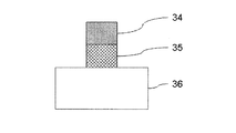
- reference numeral 34 denotes an electrode film
- reference numeral 35 denotes a TMR element, a GMR element, or the like.
- Reference numeral 36 denotes a substrate.
- the steps shown in FIG. 2 for forming a layer that also functions as a magnetic film processing mask and a magnetic film are described below.
- the laminated body is obtained by laminating the magnetic film 35, the electrode film 34, the Ru film 33, and the insulating silicon compound film 32 in this order.
- the electrode film 34 is formed on the substrate 36 on which the magnetic film 35 is formed.
- Other configurations may exist between the magnetic film 35 and the substrate 36.
- the magnetic film 35 may be formed in a consistent vacuum in the same apparatus as the vacuum apparatus in which the insulating silicon compound film 32 is formed from the electrode film 34, or the magnetic film 35 is formed from another apparatus. You may bring your own board.
- the Ru film 33 and the insulating silicon compound film 32 are sequentially formed on the electrode film 34.
- various film formation methods such as sputtering and CVD (Chemical Vapor Deposition) are used.
- a photoresist 31 is formed on the insulating silicon compound film 32.
- the film formation from the electrode film 34 to the photoresist 31 may be performed consistently in a vacuum, or after the film formation from the electrode film 34 to the insulating silicon compound film 32 is formed, it is taken out into the atmosphere and put into another apparatus.
- the photoresist 31 may be deposited after the transfer.
- the photoresist 31 is patterned by photolithography to form a desired pattern (hereinafter, the patterned photoresist 31 is also referred to as a first mask).
- FIG. 2 shows a state after the photoresist 31 is patterned.
- a pattern is transferred to the lower insulating silicon compound film 32 by RIE (hereinafter, the patterned insulating silicon compound film 32 is transferred to the second insulating silicon compound film 32).
- a fluorine-containing gas is used as the first etching gas for RIE.
- fluorocarbon is preferably used as the fluorine-containing gas.
- an inert gas such as Ar may be appropriately added to the etching gas.
- any gas may be used as long as the insulating silicon compound film 32 can be etched with the pattern of the first mask by plasma using the first mask.
- the insulating silicon compound film 32 is made of a material capable of taking a selective ratio in the fluorine-containing gas with respect to the photoresist, for example, a SiO 2 film, a SiN film, a SiON film, etc., and these single layer films or these films are used at least.
- a laminated film including two is used. That is, as the insulating silicon compound film 32, any insulating silicon compound may be used as long as the first etching gas has a high selectivity with respect to the first mask.
- the pattern is transferred to the lower Ru film 33 by RIE (hereinafter, the patterned Ru film is also referred to as a third mask).
- An oxygen-containing gas such as O 2 is used as the second etching gas for RIE.
- O 2 may contain a trace amount of a halogen-based gas such as fluorocarbon, chlorine, or an inert gas.
- the Ru film 33 can be etched with the pattern of the second mask using the second mask by plasma, and the etching rate with respect to the insulating silicon compound film 32 is increased.
- any gas may be used. Note that the photoresist 31 is completely removed by the oxygen-containing gas plasma when the Ru film 33 is processed.
- FIG. 3 shows a state where the Ru film 33 is processed. Further, the insulating silicon compound film 32 is hardly etched by the processing of the Ru film 33 because of its low reactivity to the oxygen-containing gas. That is, in this step, the Ru film 33 is etched by the second etching gas using the second mask so that the insulating silicon compound film 32 remains on the Ru film 33.
- the etching rate is a film thickness in which a single layer film to be measured for the etching rate is separately formed on the substrate, and each single layer film is etched per unit time under the same conditions. Pointing.
- the pattern is transferred to the electrode film 34 below the Ru film 33 by RIE (hereinafter, the processed electrode film 34 is changed to the first mask). 4).
- a chlorine-containing gas such as Cl 2 or BCl 3 , or a mixed gas of BCl and Cl 2 is used as a third etching gas for RIE.
- an inert gas such as Ar may be added as appropriate.
- any gas may be used as the third etching gas as long as the electrode film 33 can be etched with the second mask pattern by plasma using the second mask.
- the electrode film 34 a material which has a selectivity with respect to the insulating silicon compound film 32 and functions as an electrode after the magnetic film 35 is processed is used.
- a material Ta, Ti or a nitride or carbide thereof, a single layer film containing at least one of W, or a laminated film thereof is used.
- a single layer film of Ta or Ti, a laminated film of Ta and TaC, or the like is used. That is, as the electrode film 34, any conductive material can be used as long as the third etching gas has a high selectivity with respect to the second mask.
- the electrode film 34 may be partially oxidized on the surface in consideration of selectivity with respect to the second mask. In the case where an oxidized portion is formed on the surface of the electrode film 34, the electrode film 34 can function as an electrode by removing the oxidized portion at the same time as the processing of the magnetic film 35 or by a surface treatment after the processing.
- FIG. 4 shows a state in which the electrode film 34 has been processed and the insulating silicon compound film 32 has been removed.
- the over-etching means that the etching depth obtained from the etching rate and etching time of the film to be etched is larger than the film thickness of the etching target film.
- the magnetic film 35 is processed by RIE using the third mask, the fourth mask, and the fourth etching gas.
- the RIE fourth etching gas an alcohol gas, a hydrocarbon gas, or a mixed gas of an alcohol gas and a hydrocarbon gas is preferably used.
- FIG. 5 shows a state in which the magnetic film 35 is processed using the third mask and the fourth mask.
- the insulating silicon compound film 32 and the redeposited silicon compound can be obtained without deteriorating the shapes of the third mask and the fourth mask that function as masks when processing the magnetic film. Can be removed.
- the electrode film 34 can be processed with high dimensional accuracy.
- the magnetic film 35 can be processed with high accuracy, and a magnetoresistive effect element corresponding to further miniaturization can be manufactured.
- a Ta film is formed as an electrode film 34 with a thickness of 100 nm, a Ru film 33 with a thickness of 5 nm, an insulating silicon compound film 32 with a SiO 2 film of 20 nm, and a photoresist 31 with a thickness of 80 nm.
- RIE is performed under the following conditions to simultaneously process the insulating silicon compound film 32 and the Ru film 33 which are SiO 2 films.
- RIE is performed under the following conditions to process the electrode film 34 that is a Ta film and to remove the insulating silicon compound film 32 that is a SiO 2 film.
- the SiO 2 film (insulating silicon compound film 32) on the Ru film 33 is removed, and it becomes possible to obtain a third mask and a fourth mask whose bottoms are formed vertically.
- RIE is performed using the third mask and the fourth mask under the following conditions to process the magnetic film 35.
- Etching gas CH 3 OH Source power 2000W Bias power 2000W Pressure in vacuum vessel 2 0.7Pa Substrate temperature 80 ° C
Landscapes
- Engineering & Computer Science (AREA)
- Chemical & Material Sciences (AREA)
- Nanotechnology (AREA)
- Manufacturing & Machinery (AREA)
- Crystallography & Structural Chemistry (AREA)
- Power Engineering (AREA)
- Physics & Mathematics (AREA)
- Materials Engineering (AREA)
- Mechanical Engineering (AREA)
- Metallurgy (AREA)
- Organic Chemistry (AREA)
- Theoretical Computer Science (AREA)
- Mathematical Physics (AREA)
- Drying Of Semiconductors (AREA)
- Hall/Mr Elements (AREA)
- ing And Chemical Polishing (AREA)
Abstract
本発明は、絶縁性珪素化合物(例えば、SiO2)に形成されたパターンを下層に転写する際に、下層の側壁や裾に堆積したSi化合物の除去を行い、且つ下層にパターンを転写するためのマスク形状の劣化を低減可能な、磁性膜を有する積層体、該積層体の製造方法、および磁性膜の加工方法を提供する。本発明の一実施形態に係る、磁性膜を有する積層体は、磁性膜(35)と、該磁性膜35上に形成された電極膜(34)と、該電極膜(34)上に形成されたRu膜(33)と、該Ru膜(33)上に形成された絶縁性珪素化合膜(32)とを備える。
Description
この発明は、電極膜の加工方法、磁性膜の加工方法、磁性膜を有する積層体、および該積層体の製造方法に関し、さらに詳しくは、FeNi、CoFe、FeMn、CoPt等の磁性薄膜のドライエッチングによる微細加工に有用な電極膜の加工方法、磁性膜の加工方法、磁性膜を有する積層体、および該積層体の製造方法に関するものである。
DRAM並の集積密度でSRAM並の高速性を持ち、かつ無制限に書き換え可能なメモリとして集積化磁気メモリであるMRAM(magnetic random access memory)が注目されている。又、GMR(巨大磁気抵抗)やTMR(トンネリング磁気抵抗)といった磁気抵抗素子を構成する薄膜磁気ヘッドや磁気センサー等の開発が急速に進んでいる。
磁性材料のエッチング加工方法として、磁性膜の上に非有機材からなるハードマスクを形成した、アルコールを用いた反応性イオンエッチング(以下RIEという)が知られている(特許文献1参照)。
特許文献1に開示された方法では、フォトレジストをマスクとして非有機材であるTaのパターニングを行っている。しかしこの方法ではTaとフォトレジストの選択比が低いためにフォトレジストを厚く成膜しなければならず、寸法精度が劣化してしまうという問題がある。
このフォトレジストの厚膜化の問題については、フッ素系ガスにおいて、フォトレジストに対してエッチング速度が速く、且つ塩素系ガスにおいて、Taに対してエッチング速度が遅いSiO2を、フォトレジストとTaの間に設ける事で解決することが出来る。
しかしこの解決方法によると、RIE中に、エッチングされたSi化合物がTaの側壁や裾に堆積し、Taマスクの形状が悪くなってしまうという新たな問題が生じる。さらに、この堆積したSi化合物をオーバーエッチングによって除去しようとすると、Taマスクまでもがエッチングされてしまい、やはり形状が悪くなってしまう。
このような寸法精度や形状の劣化は、素子の微細化が進むにつれ問題となってくる。
本発明は上述したような種々の問題に鑑み、絶縁性珪素化合物(例えば、SiO2)に形成されたパターンを下層に転写する際に、下層の側壁や裾に堆積したSi化合物の除去を行い、且つ下層にパターンを転写するためのマスク形状の劣化を低減可能な、電極膜の加工方法、磁性膜の加工方法、磁性膜を有する積層体、および該積層体の製造方法を提供することを目的とする。
本発明は上述したような種々の問題に鑑み、絶縁性珪素化合物(例えば、SiO2)に形成されたパターンを下層に転写する際に、下層の側壁や裾に堆積したSi化合物の除去を行い、且つ下層にパターンを転写するためのマスク形状の劣化を低減可能な、電極膜の加工方法、磁性膜の加工方法、磁性膜を有する積層体、および該積層体の製造方法を提供することを目的とする。
このような目的を達成するために、本発明の第1の態様は、電極膜の加工方法であって、磁性膜上に、電極膜とRu膜と珪素化合物を含む絶縁膜とが順次積層された積層体を用意する第1の工程と、前記絶縁膜上にフォトレジストを成膜する第2の工程と、前記フォトレジストをパターニングし第1のマスクを形成する第3の工程と、前記第1のマスクを使用して、フッ素含有ガスおよび酸素含有ガスを用いて前記絶縁膜および前記Ru膜を反応性イオンエッチングすることで、前記第1のマスクのパターンが転写された前記絶縁膜である第2のマスク、および前記第1のマスクのパターンが転写された前記Ru膜である第3のマスクを形成する第4の工程と、前記第2及び第3のマスクを使用して、塩素含有ガスを用いて前記電極膜を反応性イオンエッチングする第5の工程とを有することを特徴とする。
本発明の第2の態様は、磁性膜の加工方法であって、上記第1の態様に記載の方法によって得られた電極膜をマスクとして使用して反応性イオンエッチングすることで前記磁性膜を加工することを特徴とする。
本発明の第3の態様は、磁性膜上に、電極膜とRu膜と珪素化合物を含む絶縁膜とが順次積層された積層体が有する前記電極膜の加工方法であって、前記絶縁膜上に形成されたフォトレジストをパターニングし第1のマスクを形成する第1の工程と、前記第1のマスクを使用して、フッ素含有ガスおよび酸素含有ガスを用いて前記絶縁膜および前記Ru膜を反応性イオンエッチングすることで、前記第1のマスクのパターンが転写された前記絶縁膜である第2のマスク、および前記第1のマスクのパターンが転写された前記Ru膜である第3のマスクを形成する第2の工程と、前記第2及び第3のマスクを使用して、塩素含有ガスを用いて前記電極膜を反応性イオンエッチングする第3の工程とを有することを特徴とする。
本発明の第4の態様は、磁性膜の加工方法であって、上記第3の態様に記載の方法によって得られた電極膜をマスクとして使用して反応性イオンエッチングすることで前記磁性膜を加工することを特徴とする。
本発明の第5の態様は、磁性膜を有する積層体であって、前記磁性膜と、前記磁性膜上に形成された電極膜と、前記電極膜上に形成されたRu膜と、前記Ru膜上に形成された珪素化合物を含む絶縁膜とを備えることを特徴とする。
本発明の第6の態様は、磁性膜を有する積層体の製造方法であって、前記磁性膜が形成された基板を用意する工程と、前記磁性膜上に電極膜を成膜する工程と、前記電極膜上にRu膜を成膜する工程と、前記Ru膜上に珪素化合物を含む絶縁膜を成膜する工程と、を有することを特徴とする。
本発明の第2の態様は、磁性膜の加工方法であって、上記第1の態様に記載の方法によって得られた電極膜をマスクとして使用して反応性イオンエッチングすることで前記磁性膜を加工することを特徴とする。
本発明の第3の態様は、磁性膜上に、電極膜とRu膜と珪素化合物を含む絶縁膜とが順次積層された積層体が有する前記電極膜の加工方法であって、前記絶縁膜上に形成されたフォトレジストをパターニングし第1のマスクを形成する第1の工程と、前記第1のマスクを使用して、フッ素含有ガスおよび酸素含有ガスを用いて前記絶縁膜および前記Ru膜を反応性イオンエッチングすることで、前記第1のマスクのパターンが転写された前記絶縁膜である第2のマスク、および前記第1のマスクのパターンが転写された前記Ru膜である第3のマスクを形成する第2の工程と、前記第2及び第3のマスクを使用して、塩素含有ガスを用いて前記電極膜を反応性イオンエッチングする第3の工程とを有することを特徴とする。
本発明の第4の態様は、磁性膜の加工方法であって、上記第3の態様に記載の方法によって得られた電極膜をマスクとして使用して反応性イオンエッチングすることで前記磁性膜を加工することを特徴とする。
本発明の第5の態様は、磁性膜を有する積層体であって、前記磁性膜と、前記磁性膜上に形成された電極膜と、前記電極膜上に形成されたRu膜と、前記Ru膜上に形成された珪素化合物を含む絶縁膜とを備えることを特徴とする。
本発明の第6の態様は、磁性膜を有する積層体の製造方法であって、前記磁性膜が形成された基板を用意する工程と、前記磁性膜上に電極膜を成膜する工程と、前記電極膜上にRu膜を成膜する工程と、前記Ru膜上に珪素化合物を含む絶縁膜を成膜する工程と、を有することを特徴とする。
本発明を用いることで磁性膜を寸法精度良く加工することが可能となる。
図1を用いて、本発明を実施するためのエッチング装置について説明する。
本発明の一実施形態に係るエッチング装置1は真空容器2を有する。真空容器2は排気系21によって排気される。また、不図示のゲートバルブを開けて被処理物を積層した基板9を真空容器2内に搬入し、基板ホルダー4に保持する。基板ホルダー4に基板9を固定する方法としては、静電吸着作用を利用した静電吸着、あるいは機械的機構を利用したクランプチャックなどが用いられる。基板ホルダー4上に固定された基板9は温度制御機構41により所定の温度に維持される。
本発明の一実施形態に係るエッチング装置1は真空容器2を有する。真空容器2は排気系21によって排気される。また、不図示のゲートバルブを開けて被処理物を積層した基板9を真空容器2内に搬入し、基板ホルダー4に保持する。基板ホルダー4に基板9を固定する方法としては、静電吸着作用を利用した静電吸着、あるいは機械的機構を利用したクランプチャックなどが用いられる。基板ホルダー4上に固定された基板9は温度制御機構41により所定の温度に維持される。
ガス導入系3を動作させることにより、エッチングガスを貯蔵しているボンベから配管、バルブ、流量調整器を介して、エッチングガスを所定の流量で真空容器2内へ導入する。導入されたエッチングガスは、誘電体壁容器11内に拡散する。ここで、プラズマ形成手段を動作させる。プラズマ形成手段は、真空容器2に対して内部空間が連通するようにして気密に接続された誘電体壁容器11と、誘電体壁容器11内に誘導磁界を発生する1ターンのアンテナ12と、アンテナ12に不図示の整合器を介して伝送路15によって接続され、アンテナ12に供給する高周波電力(ソース電力)を発生させるプラズマ用高周波電源13と、誘電体壁容器11内に所定の磁界を生じさせる電磁石14等を有している。プラズマ用高周波電源13が発生させた高周波電力が伝送路15によってアンテナ12に供給された際に、1ターンのアンテナ12に電流が流れ、この結果、誘電体壁容器11の内部にプラズマが形成される。
なお、真空容器2の側壁の外側には、多数の側壁用磁石22が並べられており、真空容器2の側壁を臨む面の磁極が、隣り合う磁石同士で互いに異なるように周方向に多数並べて配置されている。これによってカスプ磁場が真空容器2の側壁の内面に沿って周方向に連なって形成され、真空容器2の側壁の内面へのプラズマの拡散が防止ないしは低減されている。この時、同時に、バイアス用高周波電源5を作動させて、エッチング処理対象物である基板9に負の直流分の電圧であるバイアス電圧が与えられ、プラズマから基板9の表面へのイオン入射エネルギーを制御している。上記のようにして形成されたプラズマが誘電体壁容器11から真空容器2内に拡散し、基板9の表面付近にまで達する。この際、基板9の表面がエッチングされる。
次に、図面を用いて本発明の実施形態について説明する。
図2において、符号31はフォトレジスト、符号32は珪素化合物からなる絶縁膜(以下絶縁性珪素化合膜という)、符号33はRu膜、符号34は電極膜、符号35はTMR素子やGMR素子などの磁性膜、符号36は基板を示す。
図2に示される、磁性膜加工用マスクとしても機能する層、および磁性膜を有する積層体を形成するための工程を以下にしめす。
上記積層体は、磁性膜35と、電極膜34と、Ru膜33と、絶縁性珪素化合膜32とをこの順番で積層させたものである。
まず、磁性膜35が形成された基板36上に、電極膜34の成膜を行う。なお磁性膜35と基板36の間には他の構成が存在していても良い。また、磁性膜35は、電極膜34から絶縁性珪素化合膜32が形成される真空装置と同一の装置内で真空一貫で成膜されても良いし、他の装置から磁性膜35が形成された基板を持ってきても良い。そして電極膜34の上にRu膜33及び絶縁性珪素化合膜32を順次成膜する。成膜方法としては、スパッタリングやCVD(Chemical Vapor Deposition)など種々の成膜方法が用いられる。
上記積層体は、磁性膜35と、電極膜34と、Ru膜33と、絶縁性珪素化合膜32とをこの順番で積層させたものである。
まず、磁性膜35が形成された基板36上に、電極膜34の成膜を行う。なお磁性膜35と基板36の間には他の構成が存在していても良い。また、磁性膜35は、電極膜34から絶縁性珪素化合膜32が形成される真空装置と同一の装置内で真空一貫で成膜されても良いし、他の装置から磁性膜35が形成された基板を持ってきても良い。そして電極膜34の上にRu膜33及び絶縁性珪素化合膜32を順次成膜する。成膜方法としては、スパッタリングやCVD(Chemical Vapor Deposition)など種々の成膜方法が用いられる。
その後、絶縁性珪素化合膜32の上にフォトレジスト31が成膜される。このとき、電極膜34からフォトレジスト31までの成膜を真空一貫で行っても良いし、電極膜34から絶縁性珪素化合膜32までを成膜した後に、大気中に取り出して別の装置に移してからフォトレジスト31が成膜されても良い。
次に、フォトリソグラフィによりフォトレジスト31のパターニングを行い、所望のパターンを形成する(以下パターニング後のフォトレジスト31を第1のマスクともいう)。フォトレジスト31がパターニングされた後の状態を図2に示す。そして、この第1のマスクおよび第1のエッチングガスを用いて、下部の絶縁性珪素化合膜32にRIEによってパターンを転写する(以下パターンニングされた後の絶縁性珪素化合膜32を第2のマスクともいう)。RIEの第1のエッチングガスとしてフッ素含有ガスを用いる。フッ素含有ガスとしては例えばフルオロカーボンが好適に用いられる。エッチングガスにはフッ素含有ガスの他に適宜Arなどの不活性ガスが添加されてもよい。本実施形態では、第1のエッチングガスとしては、プラズマにより、第1のマスクを用いて絶縁性珪素化合膜32を第1のマスクのパターンでエッチングすることができればいずれのガスを用いても良い。絶縁性珪素化合膜32には、フォトレジストに対してフッ素含有ガスにおいて選択比が取れる材質、例えばSiO2膜、SiN膜、SiON膜などが用いられ、これらの単層膜もしくはこれらの膜を少なくとも2つ含む積層膜が用いられる。すなわち、絶縁性珪素化合膜32としては、第1のエッチングガスについて、第1のマスクに対して選択比が高くなるような絶縁性珪素化合物であれば、いずれを用いても良い。
次に、第2のマスクおよび第2のエッチングガスを用いて、下部のRu膜33にRIEによってパターンを転写する(以下パターンニングされた後のRu膜を第3のマスクともいう)。RIEの第2のエッチングガスとしてO2などの酸素含有ガスを用いる。O2には微量のハロゲン系ガス、例えばフルオロカーボンや塩素、または不活性ガスなどが添加されていてもよい。本実施形態では、第2のエッチングガスとしては、プラズマにより、第2のマスクを用いてRu膜33を第2のマスクのパターンでエッチングすることができ、かつ絶縁性珪素化合膜32に対するエッチング速度がRu膜33のエッチング速度よりも低ければ(好ましくは、Ru膜33をエッチングするが、絶縁性珪素化合膜32をほとんどエッチングしない)、いずれのガスを用いても良い。なおフォトレジスト31は、このRu膜33の加工時に、酸素含有ガスのプラズマによって全て取り除かれる。Ru膜33が加工された状態を図3に示す。また絶縁性珪素化合膜32は、酸素含有ガスに対する反応性が低いため、Ru膜33の加工によってはほぼエッチングされない。すなわち、本工程では、Ru膜33上に絶縁性珪素化合膜32が残るように、上記第2のエッチングガスによりRu膜33を第2のマスクを用いてエッチングする。なお、第1のマスクを用いて、絶縁性珪素化合膜32をRIEする際に、エッチングガスをフッ素含有ガスと酸素含有ガスの混合ガスとすると、絶縁性珪素化合膜32のみならずRu膜33の加工も同時に行えるため生産性の向上が望める。
なお本明細書においてエッチング速度とは、基板上にエッチング速度の計測対象となる単層膜をそれぞれ別個に成膜し、同条件下においてそれぞれの単層膜が単位時間当たりにエッチングされる膜厚を指している。
なお本明細書においてエッチング速度とは、基板上にエッチング速度の計測対象となる単層膜をそれぞれ別個に成膜し、同条件下においてそれぞれの単層膜が単位時間当たりにエッチングされる膜厚を指している。
次に、第2のマスクおよび第3のマスク、ならびに第3のエッチングガスを用いて、Ru膜33の下部にある電極膜34にRIEによってパターンを転写する(以下加工後の電極膜34を第4のマスクともいう)。RIEの第3のエッチングガスとしてCl2またはBCl3、もしくはBClとCl2との混合ガスなどの塩素含有ガスを用いる。塩素含有ガスのほかにも適宜Arなどの不活性ガスが添加されてもよい。本実施形態では、第3のエッチングガスとしては、プラズマにより、第2のマスクを用いて電極膜33を第2のマスクのパターンでエッチングすることができればいずれのガスを用いても良い。電極膜34としては、絶縁性珪素化合膜32に対して選択比が取れ、なおかつ磁性膜35の加工後に電極として機能する材質を用いる。そのような材質としてはTa、Tiもしくはこれらの窒化物または炭化物、Wのうち少なくとも1つを含有する単層膜、もしくはこれらの積層膜が用いられる。例としては、TaやTiの単層膜、TaとTaCの積層膜などが用いられる。すなわち、電極膜34としては、第3のエッチングガスについて、第2のマスクに対して選択比が高くなるような導電性材料であれば、いずれを用いても良い。また電極膜34は、第2のマスクに対する選択性を考慮して表面部分が一部酸化していても良い。電極膜34の表面に酸化部分を形成した場合は、酸化部分を磁性膜35の加工と同時もしくは加工後の表面処理によって除去することで、電極膜34を電極として機能させることができる。
通常、絶縁性珪素化合膜32をマスクとして塩素含有ガスによってRIEを行った場合、珪素の一部が基板上に再堆積してしまいマスクの形状が悪くなる問題がある。また、この再堆積を除去するためにオーバーエッチングを行ったとしても、絶縁性珪素化合膜32の下部にある電極膜34の形状が悪くなってしまう。しかし、本実施形態によれば、珪素化合物32の下部にパターニングされたRu膜33が存在する。このRu膜33は第3のエッチングガスとしての塩素含有ガスに対して耐性を持つため、Ru膜33上に残っている絶縁性珪素化合膜32や、磁性膜35上や電極膜34の側壁に再堆積した珪素及びその化合物を除去すべくオーバーエッチングを行ったとしても、パターニングされた形状を良好に保つことができる。電極膜34が加工され、絶縁性珪素化合膜32が除去された状態を図4に示す。
なお、オーバーエッチングとは、エッチング対象膜の膜厚に対して、該膜のエッチングレートとエッチング時間から求められるエッチング深さの方が大きいことを指す。
そして、第3のマスク及び第4のマスク、ならびに第4のエッチングガスを用いて、磁性膜35をRIEによって加工する。RIEの第4のエッチングガスとしてはアルコールガス、または炭化水素ガス、あるいはアルコールガスと炭化水素ガスとの混合ガスが好適に用いられる。第3のマスク及び第4のマスクを用いて磁性膜35を加工した状態を図5に示す。
なお、磁性膜35をRIEする際に第4のエッチングガスとしてアルコールガスを用いた場合、ウェハに対して塩素含有ガスについてのアフターコロージョンの処理を行う必要がない。
このように、本実施形態によれば、磁性膜を加工するにあたってマスクとして機能する第3のマスク及び第4のマスクの形状を劣化させることなく、絶縁性珪素化合膜32及び再堆積した珪素化合物の除去を行うことが可能となる。このため、電極膜34を寸法精度良く加工することができる。また、電極膜34をマスクとして用いることで、磁性膜35の加工を精度良く行うことが可能となり、更なる微細化に対応した磁気抵抗効果素子が製造可能となる。
(実施例)
以下に本実施形態の実施例を示す。
以下に本実施形態の実施例を示す。
磁性膜35が形成された基板上に、電極膜34としてTa膜を100nm、Ru膜33を5nm、絶縁性珪素化合膜32としてSiO2膜を20nm、フォトレジスト31を80nm成膜する。
フォトレジスト31をフォトリソグラフィによりパターニングして第1のマスクを形成した後、以下の条件でRIEを行い、SiO2膜である絶縁性珪素化合膜32及びRu膜33の加工を同時に行う。
エッチングガス CF4+O2
エッチングガスの流量比 CF4:O2=9:1
ソース電力 700W
バイアス電力 100W
真空容器2内の圧力 0.3Pa
基板温度 80℃
エッチングガス CF4+O2
エッチングガスの流量比 CF4:O2=9:1
ソース電力 700W
バイアス電力 100W
真空容器2内の圧力 0.3Pa
基板温度 80℃
該RIEによって第2のマスク及び第3のマスクを形成後、以下の条件でRIEを行い、Ta膜である電極膜34の加工及びSiO2膜である絶縁性珪素化合膜32の除去を行う。
エッチングガス Cl2+BCl3+Ar
エッチングガスの流量比 Cl2+BCl3+Ar=7:1:2
ソース電力 1500W
バイアス電力 50W
真空容器2内の圧力 0.4Pa
基板温度 120℃
オーバーエッチング 75%(エッチング深さが膜厚の175%)
エッチングガス Cl2+BCl3+Ar
エッチングガスの流量比 Cl2+BCl3+Ar=7:1:2
ソース電力 1500W
バイアス電力 50W
真空容器2内の圧力 0.4Pa
基板温度 120℃
オーバーエッチング 75%(エッチング深さが膜厚の175%)
このRIEにより、Ru膜33上のSiO2膜(絶縁性珪素化合膜32)は除去され、裾が垂直状に形成された第3のマスク及び第4のマスクを得ることが可能となる。
次に、第3のマスク及び第4のマスクを用いて以下の条件でRIEを行い、磁性膜35の加工を行う。
エッチングガス CH3OH
ソース電力 2000W
バイアス電力 2000W
真空容器2内の圧力 0.7Pa
基板温度 80℃
エッチングガス CH3OH
ソース電力 2000W
バイアス電力 2000W
真空容器2内の圧力 0.7Pa
基板温度 80℃
本実施形態により得られた磁性膜をSEM及び断面TEMで確認したところ、精度良く加工されていることが確認できた。
Claims (26)
- 電極膜の加工方法であって、
磁性膜上に、電極膜とRu膜と珪素化合物を含む絶縁膜とが順次積層された積層体を用意する第1の工程と、
前記絶縁膜上にフォトレジストを成膜する第2の工程と、
前記フォトレジストをパターニングし第1のマスクを形成する第3の工程と、
前記第1のマスクを使用して、フッ素含有ガスおよび酸素含有ガスを用いて前記絶縁膜および前記Ru膜を反応性イオンエッチングすることで、前記第1のマスクのパターンが転写された前記絶縁膜である第2のマスク、および前記第1のマスクのパターンが転写された前記Ru膜である第3のマスクを形成する第4の工程と、
前記第2及び第3のマスクを使用して、塩素含有ガスを用いて前記電極膜を反応性イオンエッチングする第5の工程と
を有することを特徴とする電極膜の加工方法。 - 前記第4の工程は、
前記第1のマスクを使用して、前記フッ素含有ガスを用いて前記絶縁膜を反応性イオンエッチングすることで前記第2のマスクを形成する工程と、
前記第2のマスクを使用して、前記酸素含有ガスを用いて前記Ru膜を反応性イオンエッチングすることで前記第3のマスクを形成する工程と
を有することを特徴とする請求項1に記載の電極膜の加工方法。 - 前記第4の工程は、前記第1のマスクを使用して、前記フッ素含有ガスと前記酸素含有ガスの混合ガスを用いて、前記絶縁膜及び前記Ru膜を前記反応性イオンエッチングすることで前記第2のマスク及び前記第3のマスクを形成することを特徴とする請求項1に記載の電極膜の加工方法。
- 前記絶縁膜は、SiO2膜、SiN膜またはSiON膜、もしくはこれらの膜の少なくとも2つを含む積層膜であることを特徴とする請求項1に記載の電極膜の加工方法。
- 前記電極膜は、Ta、Tiもしくはこれらの窒化物または炭化物、Wのうち少なくとも1つを含有する単層膜、もしくはこれらの積層膜であることを特徴とする請求項1に記載の電極膜の加工方法。
- 前記フッ素含有ガスはフルオロカーボンであることを特徴とする請求項1に記載の電極膜の加工方法。
- 前記塩素含有ガスはBCl3またはCl2、もしくはBCl3とCl2の混合ガスであることを特徴とする請求項1に記載の電極膜の加工方法。
- 請求項1に記載の方法によって得られた電極膜をマスクとして使用して反応性イオンエッチングすることで前記磁性膜を加工することを特徴とする磁性膜の加工方法。
- 前記磁性膜を反応性イオンエッチングする際に用いられるガスが、アルコールガスもしくは炭化水素ガス、またはこれらの混合ガスであることを特徴とする請求項8に記載の磁性膜の加工方法。
- 請求項8に記載の磁性膜の加工方法を用いて製造された磁気抵抗効果素子。
- 磁性膜上に、電極膜とRu膜と珪素化合物を含む絶縁膜とが順次積層された積層体が有する前記電極膜の加工方法であって、
前記絶縁膜上に形成されたフォトレジストをパターニングし第1のマスクを形成する第1の工程と、
前記第1のマスクを使用して、フッ素含有ガスおよび酸素含有ガスを用いて前記絶縁膜および前記Ru膜を反応性イオンエッチングすることで、前記第1のマスクのパターンが転写された前記絶縁膜である第2のマスク、および前記第1のマスクのパターンが転写された前記Ru膜である第3のマスクを形成する第2の工程と、
前記第2及び第3のマスクを使用して、塩素含有ガスを用いて前記電極膜を反応性イオンエッチングする第3の工程と
を有することを特徴とする電極膜の加工方法。 - 前記第2の工程は、
前記第1のマスクを使用して、前記フッ素含有ガスを用いて前記絶縁膜を反応性イオンエッチングすることで前記第2のマスクを形成する工程と、
前記第2のマスクを使用して、前記酸素含有ガスを用いて前記Ru膜を反応性イオンエッチングすることで前記第3のマスクを形成する工程と
を有することを特徴とする請求項11に記載の電極膜の加工方法。 - 前記第2の工程は、前記第1のマスクを使用して、前記フッ素含有ガスと前記酸素含有ガスの混合ガスを用いて、前記絶縁膜及び前記Ru膜を前記反応性イオンエッチングすることで前記第2のマスク及び前記第3のマスクを形成することを特徴とする請求項11に記載の電極膜の加工方法。
- 前記絶縁膜は、SiO2膜、SiN膜またはSiON膜、もしくはこれらの膜の少なくとも2つを含む積層膜であることを特徴とする請求項11に記載の電極膜の加工方法。
- 前記電極膜は、Ta、Tiもしくはこれらの窒化物または炭化物、Wのうち少なくとも1つを含有する単層膜、もしくはこれらの積層膜であることを特徴とする請求項11に記載の電極膜の加工方法。
- 前記フッ素含有ガスはフルオロカーボンであることを特徴とする請求項11に記載の電極膜の加工方法。
- 前記塩素含有ガスはBCl3とCl2の混合ガスであることを特徴とする請求項11に記載の電極膜の加工方法。
- 請求項11に記載の方法によって得られた電極膜をマスクとして使用して反応性イオンエッチングすることで前記磁性膜を加工することを特徴とする磁性膜の加工方法。
- 前記磁性膜を反応性イオンエッチングする際に用いられるガスが、アルコールガスもしくは炭化水素ガス、またはこれらの混合ガスであることを特徴とする請求項18に記載の磁性膜の加工方法。
- 請求項18に記載の磁性膜の加工方法を用いて製造された磁気抵抗効果素子。
- 磁性膜を有する積層体であって、
前記磁性膜と、
前記磁性膜上に形成された電極膜と、
前記電極膜上に形成されたRu膜と、
前記Ru膜上に形成された珪素化合物を含む絶縁膜と
を備えることを特徴とする磁性膜を有する積層体。 - 前記絶縁膜は、SiO2膜、SiN膜またはSiON膜、もしくはこれらの膜の少なくとも2つを含む積層膜であることを特徴とする請求項21に記載の磁性膜を有する積層体。
- 前記電極膜は、Ta、Tiもしくはこれらの窒化物または炭化物、Wのうち少なくとも1つを含有する単層膜、もしくはこれらの積層膜であることを特徴とする請求項21に記載の磁性膜を有する積層体。
- 磁性膜を有する積層体の製造方法であって、
前記磁性膜が形成された基板を用意する工程と、
前記磁性膜上に電極膜を成膜する工程と、
前記電極膜上にRu膜を成膜する工程と、
前記Ru膜上に珪素化合物を含む絶縁膜を成膜する工程と、
を有することを特徴とする磁性膜を有する積層体の製造方法。 - 前記絶縁膜は、SiO2膜、SiN膜またはSiON膜、もしくはこれらの膜の少なくとも2つを含む積層膜であることを特徴とする請求項24に記載の磁性膜を有する積層体の製造方法。
- 前記電極膜は、Ta、Tiもしくはこれらの窒化物または炭化物、Wのうち少なくとも1つを含有する単層膜、もしくはこれらの積層膜であることを特徴とする請求項24に記載の磁性膜を有する積層体の製造方法。
Priority Applications (1)
| Application Number | Priority Date | Filing Date | Title |
|---|---|---|---|
| JP2012550724A JP5639195B2 (ja) | 2010-12-27 | 2011-12-26 | 電極膜の加工方法、磁性膜の加工方法、磁性膜を有する積層体、および該積層体の製造方法 |
Applications Claiming Priority (2)
| Application Number | Priority Date | Filing Date | Title |
|---|---|---|---|
| JP2010291273 | 2010-12-27 | ||
| JP2010-291273 | 2010-12-27 |
Publications (1)
| Publication Number | Publication Date |
|---|---|
| WO2012090474A1 true WO2012090474A1 (ja) | 2012-07-05 |
Family
ID=46382611
Family Applications (1)
| Application Number | Title | Priority Date | Filing Date |
|---|---|---|---|
| PCT/JP2011/007269 Ceased WO2012090474A1 (ja) | 2010-12-27 | 2011-12-26 | 電極膜の加工方法、磁性膜の加工方法、磁性膜を有する積層体、および該積層体の製造方法 |
Country Status (2)
| Country | Link |
|---|---|
| JP (1) | JP5639195B2 (ja) |
| WO (1) | WO2012090474A1 (ja) |
Cited By (3)
| Publication number | Priority date | Publication date | Assignee | Title |
|---|---|---|---|---|
| JP2014212310A (ja) * | 2013-04-02 | 2014-11-13 | 東京エレクトロン株式会社 | 半導体デバイスの製造方法及び製造装置 |
| JP2016143982A (ja) * | 2015-01-30 | 2016-08-08 | 富士通株式会社 | 情報処理装置 |
| CN107004760A (zh) * | 2014-12-18 | 2017-08-01 | 英特尔公司 | 用于从原位沉积的磁性叠层制造自旋逻辑器件的方法 |
Citations (3)
| Publication number | Priority date | Publication date | Assignee | Title |
|---|---|---|---|---|
| JPH05114118A (ja) * | 1991-10-23 | 1993-05-07 | Sharp Corp | 薄膜磁気ヘツドの製造方法 |
| WO2009096328A1 (ja) * | 2008-01-29 | 2009-08-06 | Ulvac, Inc. | 磁気デバイスの製造方法 |
| JP2010040083A (ja) * | 2008-08-01 | 2010-02-18 | Fujitsu Ltd | 磁気ヘッドの製造方法 |
-
2011
- 2011-12-26 WO PCT/JP2011/007269 patent/WO2012090474A1/ja not_active Ceased
- 2011-12-26 JP JP2012550724A patent/JP5639195B2/ja active Active
Patent Citations (3)
| Publication number | Priority date | Publication date | Assignee | Title |
|---|---|---|---|---|
| JPH05114118A (ja) * | 1991-10-23 | 1993-05-07 | Sharp Corp | 薄膜磁気ヘツドの製造方法 |
| WO2009096328A1 (ja) * | 2008-01-29 | 2009-08-06 | Ulvac, Inc. | 磁気デバイスの製造方法 |
| JP2010040083A (ja) * | 2008-08-01 | 2010-02-18 | Fujitsu Ltd | 磁気ヘッドの製造方法 |
Cited By (6)
| Publication number | Priority date | Publication date | Assignee | Title |
|---|---|---|---|---|
| JP2014212310A (ja) * | 2013-04-02 | 2014-11-13 | 東京エレクトロン株式会社 | 半導体デバイスの製造方法及び製造装置 |
| CN107004760A (zh) * | 2014-12-18 | 2017-08-01 | 英特尔公司 | 用于从原位沉积的磁性叠层制造自旋逻辑器件的方法 |
| EP3235018A4 (en) * | 2014-12-18 | 2018-08-15 | Intel Corporation | Method for fabricating spin logic devices from in-situ deposited magnetic stacks |
| US10600957B2 (en) | 2014-12-18 | 2020-03-24 | Intel Corporation | Method for fabricating spin logic devices from in-situ deposited magnetic stacks |
| CN107004760B (zh) * | 2014-12-18 | 2020-11-03 | 英特尔公司 | 用于从原位沉积的磁性叠层制造自旋逻辑器件的方法 |
| JP2016143982A (ja) * | 2015-01-30 | 2016-08-08 | 富士通株式会社 | 情報処理装置 |
Also Published As
| Publication number | Publication date |
|---|---|
| JP5639195B2 (ja) | 2014-12-10 |
| JPWO2012090474A1 (ja) | 2014-06-05 |
Similar Documents
| Publication | Publication Date | Title |
|---|---|---|
| KR101574155B1 (ko) | 자기 저항 효과 소자의 제조 방법 | |
| US8546263B2 (en) | Method of patterning of magnetic tunnel junctions | |
| US6841484B2 (en) | Method of fabricating a magneto-resistive random access memory (MRAM) device | |
| JP4111274B2 (ja) | 磁性材料のドライエッチング方法 | |
| KR101066158B1 (ko) | 자기 소자의 제조 방법 및 제조 장치 | |
| KR100976882B1 (ko) | 반도체 장치의 제조 방법 및 기억 매체 | |
| US10157961B2 (en) | Method of manufacturing magnetoresistive element | |
| WO2013027406A1 (ja) | 磁気抵抗効果素子の製造方法及び磁気抵抗効果膜の加工方法 | |
| CN103794717B (zh) | 一种包含介电层的嵌入型磁隧道结器件的制造方法 | |
| JP4605554B2 (ja) | ドライエッチング用マスク材 | |
| JPWO2008129605A1 (ja) | 磁性素子の製造法 | |
| JP2008065944A (ja) | 磁性層パターンの形成方法、磁気抵抗素子の製造方法、及び磁気記憶媒体の製造方法 | |
| WO2010084909A1 (ja) | 磁性膜加工チャンバのクリーニング方法、磁性素子の製造方法、および基板処理装置 | |
| JP7339032B2 (ja) | 基板処理方法および基板処理装置 | |
| JP5639195B2 (ja) | 電極膜の加工方法、磁性膜の加工方法、磁性膜を有する積層体、および該積層体の製造方法 | |
| US20100301008A1 (en) | Process and apparatus for fabricating magnetic device | |
| JP4905969B2 (ja) | 磁気デバイスの製造装置 | |
| JP4653470B2 (ja) | エッチング方法 | |
| JP7208767B2 (ja) | 磁気抵抗素子の製造方法及び製造装置 | |
| WO2016079818A1 (ja) | プラズマ処理方法 | |
| JPWO2009084445A1 (ja) | ドライエッチング方法、磁気抵抗効果素子とその製造方法及び製造装置 | |
| WO2016027388A1 (ja) | 磁気抵抗効果素子の製造方法および製造システム |
Legal Events
| Date | Code | Title | Description |
|---|---|---|---|
| 121 | Ep: the epo has been informed by wipo that ep was designated in this application |
Ref document number: 11853741 Country of ref document: EP Kind code of ref document: A1 |
|
| DPE1 | Request for preliminary examination filed after expiration of 19th month from priority date (pct application filed from 20040101) | ||
| ENP | Entry into the national phase |
Ref document number: 2012550724 Country of ref document: JP Kind code of ref document: A |
|
| NENP | Non-entry into the national phase |
Ref country code: DE |
|
| 122 | Ep: pct application non-entry in european phase |
Ref document number: 11853741 Country of ref document: EP Kind code of ref document: A1 |