WO2012081574A1 - 粘着剤層付き透明導電性フィルム、その製造方法及びタッチパネル - Google Patents
粘着剤層付き透明導電性フィルム、その製造方法及びタッチパネル Download PDFInfo
- Publication number
- WO2012081574A1 WO2012081574A1 PCT/JP2011/078787 JP2011078787W WO2012081574A1 WO 2012081574 A1 WO2012081574 A1 WO 2012081574A1 JP 2011078787 W JP2011078787 W JP 2011078787W WO 2012081574 A1 WO2012081574 A1 WO 2012081574A1
- Authority
- WO
- WIPO (PCT)
- Prior art keywords
- adhesive layer
- sensitive adhesive
- pressure
- layer
- film
- Prior art date
- Legal status (The legal status is an assumption and is not a legal conclusion. Google has not performed a legal analysis and makes no representation as to the accuracy of the status listed.)
- Ceased
Links
Images



Classifications
-
- C—CHEMISTRY; METALLURGY
- C09—DYES; PAINTS; POLISHES; NATURAL RESINS; ADHESIVES; COMPOSITIONS NOT OTHERWISE PROVIDED FOR; APPLICATIONS OF MATERIALS NOT OTHERWISE PROVIDED FOR
- C09J—ADHESIVES; NON-MECHANICAL ASPECTS OF ADHESIVE PROCESSES IN GENERAL; ADHESIVE PROCESSES NOT PROVIDED FOR ELSEWHERE; USE OF MATERIALS AS ADHESIVES
- C09J7/00—Adhesives in the form of films or foils
- C09J7/30—Adhesives in the form of films or foils characterised by the adhesive composition
- C09J7/38—Pressure-sensitive adhesives [PSA]
-
- G—PHYSICS
- G06—COMPUTING OR CALCULATING; COUNTING
- G06F—ELECTRIC DIGITAL DATA PROCESSING
- G06F3/00—Input arrangements for transferring data to be processed into a form capable of being handled by the computer; Output arrangements for transferring data from processing unit to output unit, e.g. interface arrangements
- G06F3/01—Input arrangements or combined input and output arrangements for interaction between user and computer
- G06F3/03—Arrangements for converting the position or the displacement of a member into a coded form
- G06F3/041—Digitisers, e.g. for touch screens or touch pads, characterised by the transducing means
- G06F3/0412—Digitisers structurally integrated in a display
-
- G—PHYSICS
- G06—COMPUTING OR CALCULATING; COUNTING
- G06F—ELECTRIC DIGITAL DATA PROCESSING
- G06F3/00—Input arrangements for transferring data to be processed into a form capable of being handled by the computer; Output arrangements for transferring data from processing unit to output unit, e.g. interface arrangements
- G06F3/01—Input arrangements or combined input and output arrangements for interaction between user and computer
- G06F3/03—Arrangements for converting the position or the displacement of a member into a coded form
- G06F3/041—Digitisers, e.g. for touch screens or touch pads, characterised by the transducing means
- G06F3/044—Digitisers, e.g. for touch screens or touch pads, characterised by the transducing means by capacitive means
- G06F3/0443—Digitisers, e.g. for touch screens or touch pads, characterised by the transducing means by capacitive means using a single layer of sensing electrodes
-
- G—PHYSICS
- G06—COMPUTING OR CALCULATING; COUNTING
- G06F—ELECTRIC DIGITAL DATA PROCESSING
- G06F3/00—Input arrangements for transferring data to be processed into a form capable of being handled by the computer; Output arrangements for transferring data from processing unit to output unit, e.g. interface arrangements
- G06F3/01—Input arrangements or combined input and output arrangements for interaction between user and computer
- G06F3/03—Arrangements for converting the position or the displacement of a member into a coded form
- G06F3/041—Digitisers, e.g. for touch screens or touch pads, characterised by the transducing means
- G06F3/044—Digitisers, e.g. for touch screens or touch pads, characterised by the transducing means by capacitive means
- G06F3/0445—Digitisers, e.g. for touch screens or touch pads, characterised by the transducing means by capacitive means using two or more layers of sensing electrodes, e.g. using two layers of electrodes separated by a dielectric layer
-
- H—ELECTRICITY
- H01—ELECTRIC ELEMENTS
- H01B—CABLES; CONDUCTORS; INSULATORS; SELECTION OF MATERIALS FOR THEIR CONDUCTIVE, INSULATING OR DIELECTRIC PROPERTIES
- H01B13/00—Apparatus or processes specially adapted for manufacturing conductors or cables
- H01B13/0036—Details
-
- Y—GENERAL TAGGING OF NEW TECHNOLOGICAL DEVELOPMENTS; GENERAL TAGGING OF CROSS-SECTIONAL TECHNOLOGIES SPANNING OVER SEVERAL SECTIONS OF THE IPC; TECHNICAL SUBJECTS COVERED BY FORMER USPC CROSS-REFERENCE ART COLLECTIONS [XRACs] AND DIGESTS
- Y10—TECHNICAL SUBJECTS COVERED BY FORMER USPC
- Y10T—TECHNICAL SUBJECTS COVERED BY FORMER US CLASSIFICATION
- Y10T428/00—Stock material or miscellaneous articles
- Y10T428/24—Structurally defined web or sheet [e.g., overall dimension, etc.]
- Y10T428/24802—Discontinuous or differential coating, impregnation or bond [e.g., artwork, printing, retouched photograph, etc.]
-
- Y—GENERAL TAGGING OF NEW TECHNOLOGICAL DEVELOPMENTS; GENERAL TAGGING OF CROSS-SECTIONAL TECHNOLOGIES SPANNING OVER SEVERAL SECTIONS OF THE IPC; TECHNICAL SUBJECTS COVERED BY FORMER USPC CROSS-REFERENCE ART COLLECTIONS [XRACs] AND DIGESTS
- Y10—TECHNICAL SUBJECTS COVERED BY FORMER USPC
- Y10T—TECHNICAL SUBJECTS COVERED BY FORMER US CLASSIFICATION
- Y10T428/00—Stock material or miscellaneous articles
- Y10T428/24—Structurally defined web or sheet [e.g., overall dimension, etc.]
- Y10T428/24802—Discontinuous or differential coating, impregnation or bond [e.g., artwork, printing, retouched photograph, etc.]
- Y10T428/24851—Intermediate layer is discontinuous or differential
- Y10T428/24868—Translucent outer layer
Definitions
- the present invention relates to a transparent conductive film with an adhesive layer having a transparent conductor layer on one side of a film substrate and an adhesive layer on the other side, and a method for producing the same.
- the transparent conductive film with an adhesive layer of this invention is used suitably for the electrode substrate of the input device of an electrostatic capacitance type touch panel.
- the touch panel provided with the transparent conductive film with the adhesive layer of the present invention is used for, for example, a liquid crystal monitor, a liquid crystal television, a digital video camera, a digital camera, a mobile phone, a portable game machine, a car navigation, electronic paper, an organic EL display, and the like. Can be done.
- the transparent conductive film in which a transparent conductor layer (for example, an ITO film) is laminated on a transparent film substrate is known.
- the transparent conductive film is a transparent conductive film with a pressure-sensitive adhesive layer in which a pressure-sensitive adhesive layer is provided for bonding with other members on the side where the transparent conductive layer is not provided on the film base. Used.
- Patent Document 1 a pattern obtained by patterning the transparent conductive layer is used.
- a transparent conductive film with a pressure-sensitive adhesive layer having such a patterned transparent conductive layer is used by being laminated with other transparent conductive films and the like, and can be operated with two or more fingers at the same time. It is preferably used for an apparatus.
- the transparent conductor layer is patterned, a step is generated in the transparent conductor layer due to the patterning, and the difference between the patterned portion and the non-patterned portion is clarified and the appearance is poor. That is, when external light from the viewing surface side is reflected by the transparent conductor layer, or when internal light from the display element side is transmitted through the transparent conductor layer, the presence or absence of patterning becomes clear and the appearance deteriorates. It was.
- the transparent conductor layer is formed via an anchor coat layer composed of a high refractive index layer and a low refractive index layer, and by adjusting the film thickness of each anchor coat layer, A transparent conductive film that makes it difficult to see the pattern has been proposed (Patent Document 2).
- Patent Document 3 a transparent conductive film in which a pattern of the transparent conductor layer is difficult to see by laminating a layer that reduces light transmittance such as a colored layer on the transparent conductive film has been proposed (Patent Document 3).
- the unpleasant appearance due to the patterning was particularly remarkable when the transparent conductive film was subjected to a heat treatment in order to crystallize the transparent conductor layer. Due to the heat treatment, a wavy wave was generated in the transparent conductive film, and the level difference of the transparent conductor layer formed by the patterning was larger than the design value (for example, when the film substrate is a polyethylene terephthalate film) This is considered to be caused by the fact that the step is 5 times or more the design value. Further, it was found that the poor appearance due to the level difference of the transparent conductor layer generated by the patterning becomes more prominent as the film substrate is thinner. In particular, when the thickness of the film substrate is 110 ⁇ m or less, the step becomes too large to be practically used.
- the transparent conductive film with a pressure-sensitive adhesive layer has a good appearance due to the level difference of the transparent conductive layer generated by patterning, which was not particularly problematic in the transparent conductive film with a pressure-sensitive adhesive layer in which a thick film base was used. It was found that the film became obvious as the film became thinner.
- the present invention is a transparent conductive film with an adhesive layer for use in a capacitive touch panel having a transparent conductor layer on one surface of a film substrate and an adhesive layer on the other surface, Even when the substrate is a thin film substrate with a thickness of 110 ⁇ m or less, and even when the transparent conductor layer is crystallized by heat treatment, the step formed by patterning is designed. It aims at providing the transparent conductive film with an adhesive layer which can prevent that it becomes larger than a value and it worsens appearance, and its manufacturing method.
- Another object of the present invention is to provide a capacitive touch panel using the transparent conductive film with the pressure-sensitive adhesive layer.
- the present inventors have completed the present invention with the following transparent conductive film with an adhesive layer.
- the present invention includes a film substrate, a transparent conductor layer that is laminated and patterned on one surface of the film substrate, and an adhesive layer that is laminated on the other surface of the film.
- a transparent conductive film with an adhesive layer used for a capacitive touch panel The film substrate has a thickness of 10 to 110 ⁇ m, The total thickness of the film substrate and the pressure-sensitive adhesive layer is 30 to 300 ⁇ m, and
- the pressure-sensitive adhesive layer relates to a transparent conductive film with a pressure-sensitive adhesive layer, wherein the storage elastic modulus at 23 ° C. is 1.2 ⁇ 10 5 to less than 1.0 ⁇ 10 7 Pa.
- a film in which the transparent conductor layer is laminated on the film substrate through at least one undercoat layer can be used.
- the transparent conductive film with a pressure-sensitive adhesive layer a film in which the pressure-sensitive adhesive layer is laminated on the film substrate through an oligomer prevention layer can be used.
- the transparent conductive film with an adhesive layer is particularly useful when the patterned transparent conductor layer is crystallized.
- this invention is a manufacturing method of the said transparent conductive film with an adhesive layer, A transparent conductor layer is laminated on one surface of a film substrate having a thickness of 10 to 110 ⁇ m, and a storage elastic modulus at 23 ° C. is 1.2 ⁇ 10 5 to 1 on the other surface of the film substrate.
- the manufacturing method may further include a step C in which the laminate obtained in the step A is heat-treated at 60 to 200 ° C. to crystallize the transparent conductor layer in the laminate.
- the crystallization step C it is preferable to perform the crystallization step C after performing the patterning step B on the laminate obtained in the step A.
- the present invention also relates to a capacitive touch panel comprising at least one transparent conductive film with an adhesive layer.
- a transparent conductive film having a patterned transparent conductor layer has a different linear expansion coefficient between a patterned portion and a non-patterned portion of the transparent conductor layer.
- the patterning portion and the non-patterning portion of the transparent conductive film are caused by the difference in the linear expansion coefficient. It was found that the expansion and contraction behaviors differed. Then, the expansion and contraction behavior caused by the difference in the linear expansion coefficient becomes a large wavy wave in the transparent conductive film itself, the steps of the transparent conductor layer formed by the patterning become remarkable, and the appearance deteriorates. It is thought that you are doing.
- the transparent conductive laminate with a pressure-sensitive adhesive layer of the present invention is a thin film base with a film base thickness of 10 to 110 ⁇ m, and a step larger than the design value is likely to occur in the patterned transparent conductive layer.
- a pressure-sensitive adhesive layer that satisfies the predetermined range of storage elastic modulus, even when heat treatment is performed, the wavy undulation that occurs in the transparent conductive film is suppressed, and the step formed by patterning is more than the design value. Can also be prevented.
- the transparent conductive laminate with an adhesive layer of the present invention has a thin film base material
- moisture or plasticity generated from the film base material is formed. Since the amount of vapor of the agent or the like can be reduced, a high-quality transparent conductor layer can be formed.
- the transparent conductive laminate with an adhesive layer of the present invention is controlled so that the total thickness of the film substrate and the adhesive layer is 30 to 300 ⁇ m while using a thin film substrate.
- the transparent conductive laminate with the pressure-sensitive adhesive layer of the present invention is laminated and applied to the electrode substrate of the multi-touch type touch panel, the total thickness of the film substrate and the pressure-sensitive adhesive layer as described above is used. By controlling, the degree of freedom in designing the gap between the electrodes is widened, and a transparent conductive film suitable for a capacitive touch panel can be obtained with high productivity.
- the productivity is good and the adhesive satisfies the storage elastic modulus in the predetermined range. Since a layer is used, it is not necessary to add a separate process for improving the appearance, and manufacturing efficiency can be maintained high.
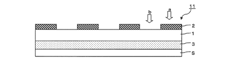
- FIG. 1 is a cross-sectional view showing an embodiment of the transparent conductive film with an adhesive layer of the present invention.
- a transparent conductive film 11 with an adhesive layer shown in FIG. 1 has a patterned transparent conductor layer 2 on one side of a film substrate 1 and an adhesive layer 3 on the other side. Yes.
- the transparent conductor layer 2 includes a patterning portion a where the transparent conductor layer is formed and a non-patterning portion b where the transparent conductor layer is not formed.
- a separator S can be bonded to the pressure-sensitive adhesive layer 3.
- the linear expansion coefficient of the patterning portion a of the transparent conductor layer 2 is preferably larger than the linear expansion coefficient of the non-patterning portion b.
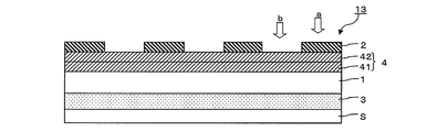
- FIGS. 2 to 4 are cross-sectional views showing a transparent conductive film with an adhesive layer according to another embodiment of the present invention.
- the transparent conductive films 12 to 14 with the pressure-sensitive adhesive layer are transparent conductors patterned on one side of the film substrate 1 via the undercoat layer 4 in the transparent conductive film 11 with the pressure-sensitive adhesive layer shown in FIG. This is an example in the case of having the layer 2.
- FIG. 2 shows a case where one undercoat layer 4 is provided.
- the undercoat layer of the present invention may have a multilayer structure of two or more layers. The case where there are two undercoat layers is shown in FIGS.
- undercoat layers 41 and 42 are provided in this order from the film substrate 1 side.
- the undercoat layer 42 is exposed through the non-patterning part b.
- the undercoat layer 42 farthest from the film substrate 1 is patterned in the same manner as the transparent conductor layer 2.
- the undercoat layer 41 is exposed through the non-patterning part b and the non-patterning part of the undercoat layer 42.
- the undercoat layer may be three or more layers.
- the first undercoat layer is preferably exposed from the film substrate 1 side.
- the undercoat layer is at least two layers, it is preferable to control the difference in reflectance between the patterned portion and the non-patterned portion to be small.
- the undercoat layer farthest from the transparent film substrate 1 (undercoat layer 42 when there are two undercoat layers 4 as shown in FIG. 4). Is preferably patterned in the same manner as the transparent conductor layer in order to control the difference in reflectance between the patterned portion and the non-patterned portion to be small.
- FIG. 5 is a cross-sectional view showing a transparent conductive film with an adhesive layer according to another embodiment of the present invention.
- the transparent conductive film 15 with an adhesive layer is an example in the case of having the adhesive layer 3 on one side of the film substrate 1 via the oligomer layer G in the transparent conductive film 11 with an adhesive layer shown in FIG. It is.
- FIG. 5 although the aspect about the transparent conductive film 11 with an adhesive layer shown in FIG. 1 is described, also about the transparent conductive films 12 to 14 with an adhesive layer shown in FIG. 2 thru
- the film substrate 1 is not particularly limited, but various plastic films having transparency are used.
- the materials include polyester resins, acetate resins, polyethersulfone resins, polycarbonate resins, polyamide resins, polyimide resins, polyolefin resins, (meth) acrylic resins, polyvinyl chloride resins, poly Examples thereof include vinylidene chloride resins, polystyrene resins, polyvinyl alcohol resins, polyarylate resins, polyphenylene sulfide resins, and the like. Of these, polyester resins, polycarbonate resins, and polyolefin resins are particularly preferable.
- a polymer film described in JP-A-2001-343529 for example, (A) a thermoplastic resin having a substituted and / or unsubstituted imide group in the side chain, and (B) a side chain.
- a thermoplastic resin having a substituted and / or unsubstituted imide group in the side chain examples thereof include resin compositions containing a substituted and / or unsubstituted phenyl and a thermoplastic resin having a nitrile group.
- a polymer film of a resin composition containing an alternating copolymer composed of isobutylene and N-methylmaleimide and an acrylonitrile / styrene copolymer can be used.
- the thickness of the film substrate 1 is 10 to 110 ⁇ m.
- the present invention is also suitable in the case of a thin thickness of 10 to 80 ⁇ m, more preferably 10 to 60 ⁇ m, and further 10 to 30 ⁇ m. If the film substrate 1 is made thin as described above, the total thickness of the transparent conductive film with the pressure-sensitive adhesive layer becomes thin. For example, when the transparent conductor layer 2 is formed by sputtering, The amount of volatile components generated from the inside of the material 1 is reduced, and as a result, a transparent conductor layer with few defects can be formed.
- the film substrate 1 may be subjected to etching treatment such as sputtering, corona discharge, flame, ultraviolet ray irradiation, electron beam irradiation, chemical conversion, oxidation, or undercoating treatment on the surface in advance.
- etching treatment such as sputtering, corona discharge, flame, ultraviolet ray irradiation, electron beam irradiation, chemical conversion, oxidation, or undercoating treatment on the surface in advance.
- etching treatment such as sputtering, corona discharge, flame, ultraviolet ray irradiation, electron beam irradiation, chemical conversion, oxidation, or undercoating treatment on the surface in advance.
- the constituent material of the transparent conductor layer 2 is not particularly limited, and is selected from the group consisting of indium, tin, zinc, gallium, antimony, titanium, silicon, zirconium, magnesium, aluminum, gold, silver, copper, palladium, and tungsten.
- a metal oxide of at least one metal is used.
- the metal oxide may further contain a metal atom shown in the above group, if necessary.
- indium oxide containing tin oxide and tin oxide containing antimony are preferably used.
- the thickness of the transparent conductor layer 2 is not particularly limited, but is preferably 10 nm or more, more preferably 15 to 40 nm, and further preferably 20 to 30 nm.
- the thickness of the transparent conductor layer 2 is 15 nm or more, the surface resistance can be easily improved to 1 ⁇ 10 3 ⁇ / ⁇ or less. Moreover, it is easy to form a continuous film. Moreover, it can be set as a layer with higher transparency as the thickness of the transparent conductor layer 2 is 40 nm or less.
- the method for forming the transparent conductor layer 2 is not particularly limited, and a conventionally known method can be employed. Specifically, for example, a vacuum deposition method, a sputtering method, and an ion plating method can be exemplified. In addition, an appropriate method can be adopted depending on the required film thickness.
- the transparent conductor layer 2 is patterned.
- the patterning of the transparent conductor layer 2 is performed by etching.
- the shape of patterning can form various shapes according to the use to which the transparent conductive film with an adhesive layer of various aspects is applied.
- examples of the shape of the patterning part include a stripe shape and a square shape.
- FIG. 9 is a plan view of the transparent conductive film with the pressure-sensitive adhesive layer shown in FIG.
- the transparent conductor layer 2 has a patterned portion a and a non-patterned portion b formed in a stripe shape.
- the width of the patterning portion a is larger than the width of the non-patterning portion b, but the present invention is not limited to this.
- the transparent conductor layer 2 preferably has a refractive index difference of 0.1 or more with respect to the undercoat layer 4 described later.
- the refractive index of the transparent conductor layer 2 is usually about 1.95 to 2.05.
- the undercoat layer 4 can be formed of an inorganic material, an organic material, or a mixture of an inorganic material and an organic material.
- NaF 1.3
- Na 3 AlF 6 (1.35)
- LiF (1.36 LiF (1.36)
- MgF 2 (1.38)
- CaF 2 1.4
- BaF 2 (1. 3)
- inorganic substances such as SiO 2 (1.46), LaF 3 (1.55), CeF 3 (1.63), Al 2 O 3 (1.63) It is a rate].
- SiO 2 , MgF 2 , A1 2 O 3 and the like are preferably used.
- SiO 2 is suitable.
- a composite oxide containing about 10 to 40 parts by weight of cerium oxide and about 0 to 20 parts by weight of tin oxide with respect to indium oxide can be used.
- examples of the organic material include acrylic resin, urethane resin, melamine resin, alkyd resin, siloxane polymer, and organic silane condensate. At least one of these organic substances is used.
- a thermosetting resin made of a mixture of a melamine resin, an alkyd resin, and an organosilane condensate.
- the undercoat layer 4 can be provided between the film substrate 1 and the transparent conductor layer 2 and does not have a function as a conductor layer. That is, the undercoat layer 4 is provided as a dielectric layer that insulates between the patterned transparent conductor layers 2. Therefore, the undercoat layer 4 usually has a surface resistance of 1 ⁇ 10 6 ⁇ / ⁇ or more, preferably 1 ⁇ 10 7 ⁇ / ⁇ or more, and more preferably 1 ⁇ 10 8 ⁇ / ⁇ or more.
- the upper limit of the surface resistance of the undercoat layer 4 is not particularly limited. In general, the upper limit of the surface resistance of the undercoat layer 4 is about 1 ⁇ 10 13 ⁇ / ⁇ , which is a measurement limit, but may exceed 1 ⁇ 10 13 ⁇ / ⁇ .
- the refractive index of the undercoat layer 4 is preferably such that the difference between the refractive index of the transparent conductor layer 2 and the refractive index of the undercoat layer is 0.1 or more.
- the difference between the refractive index of the transparent conductor layer 2 and the refractive index of the undercoat layer is preferably from 0.1 to 0.9, more preferably from 0.1 to 0.6.
- the refractive index of the undercoat layer 4 is usually 1.3 to 2.5, more preferably 1.38 to 2.3, and further preferably 1.4 to 2.3.
- the first undercoat layer (for example, the undercoat layer 41) from the film substrate 1 is preferably formed of an organic material when patterning the transparent conductor layer 2 by etching.
- the undercoat layer 4 is one layer (for example, in the case of the undercoat layer 4 shown in FIG. 2), the undercoat layer 4 is preferably formed of an organic material.
- At least the undercoat layer (for example, the undercoat layer 42) farthest from the film substrate 1 is formed of an inorganic material. 2 is preferable for patterning by etching.
- the undercoat layer above the second layer from the film substrate 1 is also preferably formed of an inorganic material.
- the undercoat layer formed of an inorganic material can be formed as a dry process such as a vacuum deposition method, a sputtering method, or an ion plating method, or by a wet method (coating method).
- a wet method coating method
- SiO 2 is preferable as described above.
- a SiO 2 film can be formed by applying silica sol or the like.
- first undercoat layer 41 with an organic material
- second undercoat layer 42 with an inorganic material
- the thickness of the undercoat layer 4 is not particularly limited, but is usually about 1 to 300 nm, preferably 5 to 300 nm, from the viewpoint of optical design and the effect of preventing oligomer formation from the film substrate 1. is there. When two or more undercoat layers 4 are provided, the thickness of each layer is about 5 to 250 nm, preferably 10 to 250 nm.
- the pressure-sensitive adhesive layer 3 is used for incorporating and fixing a transparent conductive film in an input device such as a touch panel.
- the pressure-sensitive adhesive layer 3 has a storage elastic modulus at 23 ° C. of 1.2 ⁇ 10 5 to less than 1.0 ⁇ 10 7 Pa. Since the pressure-sensitive adhesive layer 3 having such a storage elastic modulus is used by being laminated on the film base material 1, when the film base material 1 is bonded to a rigid base material, a force to keep the film base material 1 more flat works. The patterning step of the transparent conductor layer is greatly suppressed.
- the storage elastic modulus of the pressure-sensitive adhesive layer 3 is preferably 1.5 ⁇ 10 5 Pa or more, and more preferably 2.0 ⁇ 10 5 Pa or more.
- the storage elastic modulus of the pressure-sensitive adhesive layer 3 is preferably 5.0 ⁇ 10 6 Pa or less. If the storage elastic modulus of the pressure-sensitive adhesive layer 3 is less than 1.2 ⁇ 10 5 Pa, the patterning step may not be sufficiently reduced, while the storage elastic modulus is 1.0 ⁇ 10 7 Pa or more. There exists a possibility that the adhesive characteristic of an adhesive layer may be impaired.
- the storage elastic modulus of the pressure-sensitive adhesive layer 3 is the type of base polymer related to the pressure-sensitive adhesive, Tg (for example, the value of the storage elastic modulus can be increased by increasing the Tg of the base polymer), the type of cross-linking agent, and the formulation
- Tg for example, the value of the storage elastic modulus can be increased by increasing the Tg of the base polymer
- the type of cross-linking agent for example, the amount of the storage elastic modulus can be increased by increasing the blending amount of the crosslinking agent
- it can be appropriately increased or decreased. For example, increasing the proportion of the crosslinker increases the storage modulus and decreases the storage modulus that reduces the crosslinker.
- the pressure-sensitive adhesive layer 3 can be used without particular limitation as long as it satisfies the above storage elastic modulus.
- acrylic polymers silicone polymers, polyesters, polyurethanes, polyamides, polyvinyl ethers, vinyl acetate / vinyl chloride copolymers, modified polyolefins, epoxy systems, fluorine systems, natural rubbers, rubbers such as synthetic rubbers, etc.
- Those having the above polymer as a base polymer can be appropriately selected and used.
- an acrylic pressure-sensitive adhesive is preferably used from the viewpoint that it is excellent in optical transparency, exhibits adhesive properties such as appropriate wettability, cohesiveness and adhesiveness, and is excellent in weather resistance and heat resistance.
- acrylic pressure-sensitive adhesive examples include, as a base polymer, a (meth) acrylic polymer (A) segment having a glass transition temperature of 0 ° C. or lower and a (meth) acrylic polymer having a glass transition temperature of 40 ° C. or higher ( B) An adhesive containing a block copolymer having a segment or a graft copolymer can be used.
- the glass transition temperature of the (meth) acrylic polymer (A) segment is 0 ° C. or lower, and imparts wettability to the adherend and flexibility as a pressure sensitive adhesive at normal operating temperatures. Adhesive force is developed in the agent layer.
- the glass transition temperature of the (meth) acrylic polymer (A) segment is preferably ⁇ 20 ° C. or lower, more preferably ⁇ 30 ° C. or lower. Usually, the glass transition temperature is ⁇ 70 ° C. or higher.
- the glass transition temperature of the (meth) acrylic polymer (A) segment is preferably ⁇ 20 ° C. or less from the viewpoint of excellent durability under low temperature conditions.
- the glass transition temperature of the (meth) acrylic polymer (B) segment is 40 ° C. or higher, imparting cohesive force at normal use temperature, and having excellent adhesive properties and durability in the adhesive layer of the present invention.
- the glass transition temperature of the (meth) acrylic polymer (B) segment is preferably 80 ° C. or higher, more preferably 100 ° C. or higher, and usually the glass transition temperature is 150 ° C. or lower.
- the glass transition temperature of the (meth) acrylic polymer (B) segment is preferably 80 ° C. or higher in view of excellent durability under high temperature conditions.
- the block copolymer or graft copolymer those having the (meth) acrylic polymer (A) segment and the (meth) acrylic polymer (B) segment can be used.
- the block copolymer is represented by, for example, AB.
- the graft copolymer include those having A or B as a main chain and a segment different from the main chain as a side chain.
- each A and B may be the same or different.
- the block copolymer or graft copolymer can be used, but the block copolymer is preferable from the viewpoint of easy control of the glass transition temperature and the molecular weight, and the block copolymer.
- the block copolymer it is preferable to use a triblock copolymer represented by BAB, because it is easier to control the adhesive properties and bulk physical properties.
- the block copolymer or graft copolymer has a weight average molecular weight of 50,000 to 300,000, preferably 60,000 to 250,000 from the viewpoint of both durability and reworkability. More preferably, it is 70,000 to 200,000.
- the molecular weight distribution (Mw / Mn) of the block copolymer or graft copolymer is 1.0 to 1.5. From the viewpoint of high cohesion at high temperatures and excellent durability, 1.0 to 1. 4 is preferable, and 1.0 to 1.3 is more preferable.
- the (meth) acrylic polymer (A) segment contains (meth) acrylic acid alkyl ester as the main component of the monomer unit and the glass transition temperature satisfies 0 ° C. or less
- the type of monomer unit and The component composition is not particularly limited, but 50% by weight or more, further 60% by weight or more of the total monomer units are preferably (meth) acrylic acid alkyl esters in terms of controlling the glass transition temperature.
- Examples of the (meth) acrylic acid alkyl ester that is the main monomer unit of the (meth) acrylic polymer (A) segment include (meth) acrylic acid alkyl esters having an alkyl group with 1 to 18 carbon atoms. . Specifically, methyl (meth) acrylate, ethyl (meth) acrylate, propyl (meth) acrylate, n-butyl (meth) acrylate, t-butyl (meth) acrylate, n (meth) acrylic acid -Hexyl, cyclohexyl (meth) acrylate, 2-ethylhexyl (meth) acrylate, n-octyl (meth) acrylate, lauryl (meth) acrylate, tridecyl (meth) acrylate, stearyl (meth) acrylate, etc.
- the (meth) acrylic polymer (A) segment is preferably an acrylic polymer segment having an acrylic acid alkyl ester as a main monomer unit.
- the main monomer unit include alkyl acrylates having 1 to 9 carbon atoms in the alkyl group such as propyl acrylate, n-butyl acrylate, 2-ethylhexyl acrylate, and n-octyl acrylate. Is preferred.
- the weight ratio of the (meth) acrylic polymer (A) segment in the block copolymer or graft copolymer is preferably 50% to 95% from the viewpoint of obtaining stable adhesive strength and durability, and 60% More preferably, it is ⁇ 85%.
- the weight ratio of the (meth) acrylic polymer (A) segment is less than 50%, the adhesive force tends to be low. Further, when the weight ratio of the (meth) acrylic polymer (A) segment is more than 95%, the cohesive force is reduced because the proportion of the (meth) acrylic polymer (B) segment is small, and the optical film.
- the (meth) acrylic polymer (B) segment contains (meth) acrylic acid alkyl ester as the main component of the monomer unit and the glass transition temperature satisfies 40 ° C. or higher
- the type of monomer unit and The component composition is not particularly limited, but 15% by weight or more, further 20% by weight or more of the total monomer units is preferably a (meth) acrylic acid alkyl ester in terms of controlling the glass transition temperature.
- Examples of the (meth) acrylic acid alkyl ester that is the main monomer unit of the (meth) acrylic polymer (B) segment include (meth) acrylic acid alkyl esters having an alkyl group with 1 to 18 carbon atoms. . Specifically, methyl (meth) acrylate, ethyl (meth) acrylate, propyl (meth) acrylate, n-butyl (meth) acrylate, t-butyl (meth) acrylate, n (meth) acrylic acid -Hexyl, cyclohexyl (meth) acrylate, 2-ethylhexyl (meth) acrylate, n-octyl (meth) acrylate, lauryl (meth) acrylate, tridecyl (meth) acrylate, stearyl (meth) acrylate, ( Examples include (meth) acrylic acid alkyl esters such as (meth) acrylic acid isobornyl
- the (meth) acrylic polymer (B) segment is preferably a methacrylic polymer segment having a methacrylic acid alkyl ester as a main monomer unit.
- the main monomer unit is preferably a methacrylic acid alkyl ester having 1 to 2 carbon atoms in an alkyl group such as methyl methacrylate or ethyl methacrylate.
- the weight ratio of the (meth) acrylic polymer (B) segment in the block copolymer or graft copolymer is a ratio other than the (meth) acrylic polymer (A) segment.
- the (meth) acrylic polymer (A) segment and the (meth) acrylic polymer (B) segment contain other monomer units as long as they are in the range of 10% by weight or less of the total monomer units of each segment. May be.
- the other monomer units include methoxyethyl (meth) acrylate, ethoxyethyl (meth) acrylate, diethylaminoethyl (meth) acrylate, 2-hydroxyethyl (meth) acrylate, (meth) acrylic acid 2 -(Meth) acrylic acid ester having a functional group such as aminoethyl, glycidyl (meth) acrylate, tetrahydrofurfuryl (meth) acrylate; (meth) acrylic acid, crotonic acid, maleic acid, maleic anhydride, fumaric acid , Vinyl monomers having a carboxyl group such as (meth) acrylamide; aromatic vinyl monomers such as styrene, ⁇
- the method for producing the block copolymer or graft copolymer includes the block copolymer or graft copolymer having the (meth) acrylic polymer (A) segment and the (meth) acrylic polymer (B) segment.
- a method according to a known method can be employed without any particular limitation.
- a method for obtaining a block copolymer having a narrow molecular weight distribution a method of living polymerizing monomers as constituent units is employed.
- Examples of such living polymerization methods include a method of polymerizing using an organic rare earth metal complex as a polymerization initiator (JP-A-6-93060), an alkali metal or an alkaline earth metal using an organic alkali metal compound as a polymerization initiator.
- Anionic polymerization in the presence of a mineral salt such as a salt see Japanese Patent Publication No. 7-25859
- anionic polymerization in the presence of an organoaluminum compound using an organic alkali metal compound as a polymerization initiator Japanese Patent Laid-Open No. Hei 11- 335432
- atom transfer radical polymerization method ATRP
- a method for obtaining a graft copolymer is disclosed in Japanese Patent No. 4228026. Examples include the method described in the specification and the like.
- Examples of the anionic polymerization method in the presence of the above organoaluminum compound include an organolithium compound and the following general formula (1): AlR 1 R 2 R 3 (1) Wherein R 1 , R 2 and R 3 are each independently an alkyl group which may have a substituent, a cycloalkyl group which may have a substituent, or an aryl which may have a substituent.
- ethers such as dimethyl ether, dimethoxyethane, diethoxyethane, 12-crown-4; triethylamine, N, N, N ′, N′-tetramethylethylenediamine, N, N, N ', N'','' -Pentamethyldiethylenetriamine, 1,1,4,7,10,10-hexamethyltriethylenetetramine, pyridine, 2,2′-dipyridyl and other nitrogen-containing compounds are further used to form (meth) acrylic acid ester A polymerization method or the like can be employed.
- organic lithium compound examples include methyl lithium, ethyl lithium, n-propyl lithium, isopropyl lithium, n-butyl lithium, sec-butyl lithium, isobutyl lithium, tert-butyl lithium, n-pentyl lithium, and n-hexyl lithium.
- Alkyllithium and alkyldilithium such as tetramethylenedilithium, pentamethylenedilithium and hexamethylenedilithium; aryllithium and aryldi such as phenyllithium, m-tolyllithium, p-tolyllithium, xylyllithium and lithium naphthalene Lithium; benzyl lithium, diphenylmethyl lithium, trityl lithium, 1,1-diphenyl-3-methylpentyl lithium, ⁇ -methylstyryl lithium, diisopropeni Aralkyllithium and aralkyldilithium such as dilithium produced by the reaction of benzene and butyllithium; lithium amides such as lithium dimethylamide, lithium diethylamide and lithium diisopropylamide; methoxylithium, ethoxylithium, n-propoxylithium, isopropoxylithium, n -Butoxylithium,
- organoaluminum compound represented by the above general formula examples include trimethylaluminum, triethylaluminum, tri-n-butylaluminum, tris-butylaluminum, tri-t-butylaluminum, triisobutylaluminum, and tri-n-hexylaluminum.
- organoaluminum compounds isobutylbis (2,6-di-tert-butyl-4-methylphenoxy) aluminum, isobutylbis (2,6-di-tert-butylphenoxy) aluminum, isobutyl [2,2 ′ -Methylenebis (4-methyl-6-tert-butylphenoxy)] aluminum and the like are easy to handle, and the polymerization of the acrylate ester can proceed without deactivation under relatively mild temperature conditions. Is particularly preferable. These may be used alone or in combination of two or more.
- an acrylic polymer having an alkyl (meth) acrylate monomer unit as a main skeleton as a base polymer and a crosslinking agent added thereto can be used.
- (Meth) acrylate refers to acrylate and / or methacrylate, and (meth) of the present invention has the same meaning.
- the alkyl group of the alkyl (meth) acrylate constituting the main skeleton of the acrylic polymer has about 1 to 14 carbon atoms.
- Specific examples of the alkyl (meth) acrylate include methyl (meth) acrylate, ethyl (meth) Acrylate, propyl (meth) acrylate, isopropyl (meth) acrylate, n-butyl (meth) acrylate, isobutyl (meth) acrylate, pentyl (meth) acrylate, hexyl (meth) acrylate, 2-ethylhexyl (meth) acrylate, octyl ( Examples include (meth) acrylate, isooctyl (meth) acrylate, nonyl (meth) acrylate, isononyl (meth) acrylate, decyl (meth) acrylate, dodecyl (meth) acrylate,
- acrylic polymer one or more kinds of various monomers can be introduced by copolymerization for the purpose of improving adhesiveness and heat resistance.
- copolymerization monomers include carboxyl group-containing monomers, hydroxyl group-containing monomers, nitrogen-containing monomers (including heterocycle-containing monomers), aromatic-containing monomers, and the like.
- carboxyl group-containing monomer examples include acrylic acid, methacrylic acid, carboxyethyl (meth) acrylate, carboxypentyl (meth) acrylate, itaconic acid, maleic acid, fumaric acid, and crotonic acid.
- acrylic acid and methacrylic acid are preferable.
- hydroxyl group-containing monomers examples include 2-hydroxyethyl (meth) acrylate, 2-hydroxypropyl (meth) acrylate, 4-hydroxybutyl (meth) acrylate, 6-hydroxyhexyl (meth) acrylate, and 8-hydroxyoctyl (meth) acrylate.
- Examples thereof include 10-hydroxydecyl (meth) acrylate, 12-hydroxylauryl (meth) acrylate, and (4-hydroxymethylcyclohexyl) -methyl acrylate.
- nitrogen-containing monomer examples include maleimide, N-cyclohexylmaleimide, N-phenylmaleimide; N-acryloylmorpholine; (meth) acrylamide, N, N-dimethyl (meth) acrylamide, N, N-diethyl ( (Meth) acrylamide, N-hexyl (meth) acrylamide, N-methyl (meth) acrylamide, N-butyl (meth) acrylamide, N-butyl (meth) acrylamide, N-methylol (meth) acrylamide, N-methylolpropane (meta) ) (N-substituted) amide monomers such as acrylamide; aminoethyl (meth) acrylate, aminopropyl (meth) acrylate, N, N-dimethylaminoethyl (meth) acrylate, t-butyl (meth) acrylate Aminoethyl, 3- (3-pyri (
- aromatic-containing monomer examples include benzyl (meth) acrylate, phenyl (meth) acrylate, phenoxyethyl (meth) acrylate, and the like.
- acid anhydride group-containing monomers such as maleic anhydride and itaconic anhydride; caprolactone adducts of acrylic acid; styrene sulfonic acid and allyl sulfonic acid, 2- (meth) acrylamide-2-methylpropane sulfonic acid And sulfonic acid group-containing monomers such as (meth) acrylamide propanesulfonic acid, sulfopropyl (meth) acrylate, and (meth) acryloyloxynaphthalene sulfonic acid; and phosphoric acid group-containing monomers such as 2-hydroxyethylacryloyl phosphate.
- a hydroxyl group-containing monomer is preferably used because of its good reactivity with the crosslinking agent.
- carboxyl group-containing monomers such as acrylic acid are preferably used.
- the ratio of the copolymerization monomer in the acrylic polymer is not particularly limited, but is 50% by weight or less in terms of weight ratio. It is preferably 0.1 to 10% by weight, more preferably 0.5 to 8% by weight, and still more preferably 1 to 6% by weight.
- the average molecular weight of the acrylic polymer is not particularly limited, but the weight average molecular weight is preferably about 300,000 to 2.5 million.
- the acrylic polymer can be produced by various known methods. For example, a radical polymerization method such as a bulk polymerization method, a solution polymerization method, or a suspension polymerization method can be appropriately selected.
- a radical polymerization method such as a bulk polymerization method, a solution polymerization method, or a suspension polymerization method can be appropriately selected.
- the radical polymerization initiator various known azo and peroxide initiators can be used.
- the reaction temperature is usually about 50 to 80 ° C., and the reaction time is 1 to 8 hours.
- the solution polymerization method is preferable, and ethyl acetate, toluene and the like are generally used as the solvent for the acrylic polymer.
- the cross-linking agent blended in the acrylic polymer can improve the adhesion and durability with the transparent conductive film, and can maintain the reliability at high temperatures and the shape of the adhesive itself.
- isocyanate, epoxy, peroxide, metal chelate, oxazoline, and the like can be used as appropriate.
- These crosslinking agents can be used alone or in combination of two or more.
- Isocyanate compounds include isocyanate monomers such as tolylene diisocyanate, chlorophenylene diisocyanate, hexamethylene diisocyanate, tetramethylene diisocyanate, isophorone diisocyanate, xylylene diisocyanate, diphenylmethane diisocyanate, hydrogenated diphenylmethane diisocyanate, and these isocyanates.
- Adduct isocyanate compounds in which monomers are added with trimethylolpropane and the like; isocyanurates, burette type compounds, and urethane prepolymers obtained by addition reaction of known polyether polyols, polyester polyols, acrylic polyols, polybutadiene polyols, polyisoprene polyols, etc. Examples thereof include polymer type isocyanate.
- the isocyanate-based crosslinking agent may be used singly or as a mixture of two or more, but the total content thereof is the (meth) acrylic polymer (A) 100
- the polyisocyanate compound crosslinking agent is preferably contained in an amount of 0.01 to 2 parts by weight, more preferably 0.02 to 2 parts by weight, and more preferably 0.05 to 1.5 parts by weight. More preferably, it is contained in parts by weight. It can be appropriately contained in consideration of cohesive force and prevention of peeling in a durability test.
- Peroxides include di (2-ethylhexyl) peroxydicarbonate, di (4-t-butylcyclohexyl) peroxydicarbonate, di-sec-butylperoxydicarbonate, t-butylperoxyneodecanoate , T-hexylperoxypivalate, t-butylperoxypivalate, dilauroyl peroxide, di-n-octanoyl peroxide, 1,1,3,3-tetramethylbutylperoxyisobutyrate, 1,3,3-tetramethylbutylperoxy 2-ethylhexanoate, di (4-methylbenzoyl) peroxide, dibenzoyl peroxide, t-butylperoxyisobutyrate, and the like. Of these, di (4-t-butylcyclohexyl) peroxydicarbonate,
- the peroxide may be used alone or as a mixture of two or more, but the total content is 100 weight of the (meth) acrylic polymer (A).
- the peroxide is 0.01 to 2 parts by weight, preferably 0.04 to 1.5 parts by weight, and more preferably 0.05 to 1 part by weight. . In order to adjust processability, reworkability, cross-linking stability, peelability, and the like, it is appropriately selected within this range.
- the pressure-sensitive adhesive of the present invention can contain a silane coupling agent.
- the durability can be improved by using a silane coupling agent.
- the silane coupling agent one having any appropriate functional group can be used.
- the functional group include a vinyl group, an epoxy group, an amino group, a mercapto group, a (meth) acryloxy group, an acetoacetyl group, an isocyanate group, a styryl group, and a polysulfide group.
- vinyl group-containing silane coupling agents such as vinyltriethoxysilane, vinyltripropoxysilane, vinyltriisopropoxysilane, vinyltributoxysilane; ⁇ -glycidoxypropyltrimethoxysilane, ⁇ -glycol Epoxy group-containing silane coupling agents such as sidoxypropyltriethoxysilane, 3-glycidoxypropylmethyldiethoxysilane, 2- (3,4-epoxycyclohexyl) ethyltrimethoxysilane; ⁇ -aminopropyltrimethoxysilane, N- ⁇ - (aminoethyl) - ⁇ -aminopropylmethyldimethoxysilane, N- (2-aminoethyl) 3-aminopropylmethyldimethoxysilane, ⁇ -triethoxysilyl-N- (1,3-dimethylbutylidene) Propylamine, N
- the silane coupling agent may be used alone or in combination of two or more, but the total content is 100 parts by weight of the acrylic polymer with respect to the silane coupling agent.
- the amount is preferably 0.001 to 5 parts by weight, more preferably 0.01 to 1 part by weight, further preferably 0.02 to 1 part by weight, and further preferably 0.05 to 0.6 part by weight.
- the pressure-sensitive adhesive layer 3 may be made of, for example, natural or synthetic resins, glass fibers or glass beads, fillers made of metal powder or other inorganic powders, pigments, colorants, antioxidants, etc. These appropriate additives can also be blended. Moreover, it can also be set as the adhesive layer 3 which contained the transparent fine particle and was provided with the light diffusibility.
- the transparent fine particles include, for example, conductive inorganic fine particles such as silica, calcium oxide, alumina, titania, zirconia, tin oxide, indium oxide, cadmium oxide, and antimony oxide having an average particle size of 0.5 to 20 ⁇ m.
- conductive inorganic fine particles such as silica, calcium oxide, alumina, titania, zirconia, tin oxide, indium oxide, cadmium oxide, and antimony oxide having an average particle size of 0.5 to 20 ⁇ m.
- suitable ones such as crosslinked or uncrosslinked organic fine particles made of a suitable polymer such as polymethyl methacrylate and polyurethane can be used.
- the pressure-sensitive adhesive layer 3 is usually used as a pressure-sensitive adhesive solution having a solid content concentration of about 10 to 50% by weight in which a base polymer or a composition thereof is dissolved or dispersed in a solvent.
- a solvent an organic solvent such as toluene or ethyl acetate or an adhesive such as water can be appropriately selected and used.
- the thickness of the pressure-sensitive adhesive layer 3 is controlled so that the total thickness of the thickness of the pressure-sensitive adhesive layer 3 and the thickness of the film substrate 1 is 30 to 300 ⁇ m.
- the total thickness is preferably 20 to 280 ⁇ m, more preferably 20 to 170 ⁇ m, and further preferably 20 to 110 ⁇ m.
- the thickness of the pressure-sensitive adhesive layer 3 is preferably in the range of 10 to 170 ⁇ m, more preferably 10 to 110 ⁇ m, and further preferably 10 to 80 ⁇ m.
- the pressure-sensitive adhesive layer 3 can be formed by directly applying a pressure-sensitive adhesive solution to the film substrate 1 and drying it. Moreover, a pressure-sensitive adhesive solution is applied to the separator S and dried to form a pressure-sensitive adhesive layer 3, and the pressure-sensitive adhesive layer 3 formed on the separator S is transferred to the film base 1, whereby the film base 1 The pressure-sensitive adhesive layer 3 with the separator S can be laminated.
- a separator S for example, polyester in which a transition prevention layer and / or a release layer are laminated on at least a surface of the polyester film that is bonded to the pressure-sensitive adhesive layer 3. It is preferable to use a film or the like.
- the total thickness of the separator S is preferably 30 ⁇ m or more, and more preferably in the range of 60 to 100 ⁇ m. This is to suppress deformation (dentation) of the pressure-sensitive adhesive layer 3 that is assumed to be generated by foreign matter or the like that has entered between the rolls when the pressure-sensitive adhesive layer 3 is formed and stored in a roll state.
- the migration preventing layer can be formed of an appropriate material for preventing migration of a migration component in the polyester film, particularly a low molecular weight oligomer component of the polyester.
- a material for forming the migration prevention layer an inorganic material, an organic material, or a composite material thereof can be used.
- the thickness of the migration preventing layer can be appropriately set within the range of 0.01 to 20 ⁇ m.
- the method for forming the migration preventing layer is not particularly limited, and for example, a coating method, a spray method, a spin coating method, an in-line coating method, or the like is used. Further, a vacuum deposition method, a sputtering method, an ion plating method, a spray pyrolysis method, a chemical plating method, an electroplating method, or the like can also be used.
- the release layer a layer made of an appropriate release agent such as silicone, long chain alkyl, fluorine, or molybdenum sulfide can be formed.
- the thickness of the release layer can be appropriately set from the viewpoint of the release effect. In general, from the viewpoint of handling properties such as flexibility, the thickness is preferably 20 ⁇ m or less, more preferably in the range of 0.01 to 10 ⁇ m, and in the range of 0.1 to 5 ⁇ m. Is particularly preferred.
- the method for forming the release layer is not particularly limited, and a method similar to the method for forming the migration preventing layer can be employed.
- ionizing radiation curable resins such as acrylic resins, urethane resins, melamine resins, and epoxy resins
- the above resins include aluminum oxide and silicon dioxide.
- a mixture of mica and the like can be used.
- a vacuum deposition method, sputtering method, ion plating method, spray pyrolysis method, chemical plating method or electroplating method gold, silver, platinum, palladium, copper, aluminum, nickel, chromium, titanium, iron, It is possible to use a metal oxide made of cobalt or tin, an alloy thereof, or another metal compound made of iodide steel.
- the oligomer prevention layer G can be provided on the surface of the film base material 1 on which the pressure-sensitive adhesive layer 3 is laminated.
- the material for forming the oligomer prevention layer G an appropriate material capable of forming a transparent film is used, and an inorganic material, an organic material, or a composite material thereof may be used.
- the film thickness is preferably 0.01 to 20 ⁇ m.
- the oligomer prevention layer 5 are often used to form the oligomer prevention layer 5, but a vacuum deposition method, a sputtering method, an ion plating method, a spray heat, etc. Techniques such as a decomposition method, a chemical plating method, and an electroplating method may be used.
- a resin component such as polyvinyl alcohol resin, acrylic resin, urethane resin, melamine resin, UV curable resin, epoxy resin or a mixture of these inorganic particles such as alumina, silica, mica is used. May be.
- the base layer component may have the function of the prevention layer 5 by coextrusion of two or more polymer substrates.
- a metal made of cobalt or tin or an alloy thereof, or a metal oxide made of indium oxide, tin oxide, titanium oxide, cadmium oxide or a mixture thereof, or another metal compound made of steel iodide etc. can be used. .
- the polyvinyl alcohol-based resin has an excellent oligomer prevention function and is particularly suitable for use in the present invention.
- the polyvinyl alcohol-based resin is mainly composed of polyvinyl alcohol, and usually the content of polyvinyl alcohol is preferably in the range of 30 to 100% by weight. When the content of polyvinyl alcohol is 30% by weight or more, the effect of preventing oligomer precipitation is good.
- the resin that can be mixed with polyvinyl alcohol include water-based resins such as polyester and polyurethane.
- the degree of polymerization of polyvinyl alcohol is not particularly limited, but usually 300 to 4000 is suitable for use.
- the degree of saponification of polyvinyl alcohol is not particularly limited, but usually 70 mol% or more and 99.9 mol% or more are suitable.
- a crosslinking agent can be used in combination with the polyvinyl alcohol resin.
- Specific examples of the crosslinking agent include methylolated or alkylolized urea-based, melamine-based, guanamine-based, acrylamide-based, polyamide-based compounds, epoxy compounds, aziridine compounds, blocked isocyanates, silane coupling agents, titanium cups. Examples thereof include a ring agent and a zirco-aluminate coupling agent. These crosslinking components may be bonded in advance to the binder polymer.
- inorganic particles may be contained for the purpose of improving adhesion and slipperiness, and specific examples include silica, alumina, kaolin, calcium carbonate, titanium oxide, barium salt and the like.
- an antifoaming agent, a coating property improving agent, a thickener, an organic lubricant, organic polymer particles, an antioxidant, an ultraviolet absorber, a foaming agent, a dye, and the like may be contained as necessary.
- the total thickness of the film base 1 and the pressure-sensitive adhesive layer 3 is controlled to be 30 to 300 ⁇ m.
- the method for producing the transparent conductive film with the pressure-sensitive adhesive layer of the present invention is not particularly limited as long as the method having the above-described structure is obtained.
- the pressure-sensitive adhesive of the present invention is performed by performing the step B of patterning the transparent conductor layer in the laminate.
- a transparent conductive film with a layer can be obtained.
- a transparent conductive film which may include the undercoat layer 4
- the pressure-sensitive adhesive layer 3 is laminated on the other surface of the transparent conductive film.
- the pressure-sensitive adhesive layer 3 may be directly formed on the film base 1 as described above, or the pressure-sensitive adhesive layer 3 may be provided on the separator S and bonded to the film base 1. The latter method is more advantageous in terms of productivity because the pressure-sensitive adhesive layer 3 can be continuously formed with the film substrate 1 in a roll shape.
- patterning can be performed by etching the transparent conductor layer 2.
- the transparent conductor layer 2 is covered with a mask for forming a pattern, and the transparent conductor layer 2 is etched with an etching solution.
- the transparent conductor layer 2 is preferably made of indium oxide containing tin oxide or tin oxide containing antimony
- an acid is preferably used as the etching solution.
- the acid include inorganic acids such as hydrogen chloride, hydrogen bromide, sulfuric acid, nitric acid and phosphoric acid, organic acids such as acetic acid, and mixtures thereof, and aqueous solutions thereof.
- the transparent conductor layer 2 can be etched and patterned, and after the transparent conductor layer 2 is patterned by etching with an acid, at least the film base
- the undercoat layer farthest from the material 1 can be etched and patterned in the same manner as the transparent conductor layer 2.
- the transparent conductor layer 2 other than the first undercoat layer from the film substrate 1 can be etched and patterned in the same manner as the transparent conductor layer 2.
- the undercoat layer 4 is covered with a mask for forming a pattern similar to the case where the transparent conductor layer 2 is etched, and the undercoat layer 4 is etched with an etching solution.
- an inorganic material such as SiO 2 is preferably used for the undercoat layer above the second layer, and therefore alkali is preferably used as the etching solution.
- alkali include aqueous solutions of sodium hydroxide, potassium hydroxide, ammonia, tetramethylammonium hydroxide, and mixtures thereof.
- the first transparent conductor layer is preferably formed of an organic material that is not etched by acid or alkali.
- the refractive index (n), thickness (d), and optical thickness of each layer in the patterning portion can be as follows. Thereby, the difference of the reflectance of a patterning part and a non-patterning part can be designed small.
- the first undercoat layer 41 from the film substrate 1 can have a refractive index (n) of 1.5 to 1.7, preferably 1.5 to 1.65, and preferably 1.5 to 1. .6 is more preferable.
- the thickness (d) is preferably 100 to 220 nm, more preferably 120 to 215 nm, and further preferably 130 to 210 nm.
- the refractive index (n) of the second undercoat layer 42 from the film substrate 1 can be 1.4 to 1.5, preferably 1.41 to 1.49, and 1.42 to 1 More preferred is .48.
- the thickness (d) is preferably 20 to 80 nm, more preferably 20 to 70 nm, and further preferably 20 to 60 nm.
- the transparent conductor layer 2 can have a refractive index (n) of 1.9 to 2.1, preferably 1.9 to 2.05, and more preferably 1.9 to 2.0.
- the thickness (d) is preferably 15 to 30 nm, more preferably 15 to 28 nm, and further preferably 15 to 25 nm.
- the total optical thickness (n ⁇ d) of each layer may be 208 to 554 nm, ⁇ 500 nm is preferred, and 250 ⁇ 450 nm is more preferred.
- the difference ( ⁇ nd) between the total optical thickness of the patterning portion and the optical thickness of the undercoat layer of the non-patterning portion may be 40 to 130 nm.
- the difference in optical thickness ( ⁇ nd) is preferably 40 to 120 nm, and more preferably 40 to 110 nm.
- the laminate prepared in the step A is subjected to a heat treatment at 60 to 200 ° C. to crystallize the transparent conductor layer 2 in the laminate. Can be applied.
- the transparent conductor layer 2 is crystallized. Since the transparent conductive film with the pressure-sensitive adhesive layer of the present invention is laminated with the pressure-sensitive adhesive layer 3 having the predetermined storage elastic modulus, even when the heat treatment is performed, the swell of the film can be kept small. it can.
- the heating temperature for crystallization is usually about 60 to 200 ° C., preferably 100 to 150 ° C.
- the heat treatment time is 5 to 250 minutes. From this point of view, it is preferable that the film substrate 1 has a heat resistance of 100 ° C. or higher, more preferably 150 ° C. or higher, because the heat treatment is performed.
- the crystallization step C is preferably performed after the patterning step B is performed on the laminate prepared in the step A. Further, since the etching may be difficult when the transparent conductor layer 2 is crystallized, the crystallization step C is preferably performed after the transparent conductor layer 2 is patterned by the patterning step B. Further, when the undercoat layer 4 is etched, the crystallization step C is preferably performed after the undercoat layer 4 is etched.
- the transparent conductive film with an adhesive layer of the present invention can be used for an electrode substrate of an input device of a capacitive touch panel.
- the capacitive touch panel can adopt a multi-touch method, and the transparent conductive film with an adhesive layer of the present invention can be used as a part of the electrode substrate.
- 6 to 8 are cross-sectional views of an input device of a touch panel when the transparent conductive film 11 with an adhesive layer shown in FIG. 1 is applied to the electrode substrate.
- the conductive film 6 relates to the face-down type, and is used by laminating two transparent conductive films 11 with an adhesive layer shown in FIG. 1 on the window W so that the transparent conductive layer 2 faces downward. This is the case.
- the pressure-sensitive adhesive layer 3 of the upper transparent conductive film 11 with the pressure-sensitive adhesive layer is bonded to the window W.
- the transparent conductive film 11 with the lower pressure-sensitive adhesive layer is bonded to the film substrate 1 ′ via the pressure-sensitive adhesive layer 3 ′.
- a functional layer F is provided on the lower surface of the film substrate 1 ′.
- FIG. 7 relates to a face-up type, in which one transparent conductive film 11 with an adhesive layer shown in FIG. 1 is used with respect to the window W so that the transparent conductive layer 2 faces upward. is there.
- the transparent conductor layer 2 of the transparent conductive film 11 with the pressure-sensitive adhesive layer is bonded to the window W via the pressure-sensitive adhesive layer 3 ′.
- the transparent conductivity of another transparent conductive film (a transparent conductive layer 2 ′ patterned on the film substrate 1 ′) is provided in the adhesive layer 3 of the transparent conductive film 11 with the adhesive layer.
- the body layer 2 'side is bonded.
- a functional layer F is provided on the lower surface of the film substrate 1 ′.
- Fig. 8 relates to the double-sided type.
- the transparent conductive film 11 with the pressure-sensitive adhesive layer shown in FIG. 1 is used so that the transparent conductive layer 2 faces upward with respect to the window W, and the transparent conductive film with the pressure-sensitive adhesive layer is used.
- the transparent conductor layer 2 of the film 11 is bonded to the window W via an adhesive layer 3 ′.
- the pressure-sensitive adhesive layer 3 of the transparent conductive film 11 with a pressure-sensitive adhesive layer is a film of another transparent conductive film (one provided with a transparent conductive layer 2 ′ patterned on the film substrate 1 ′′).
- the base 1 ′′ side is bonded.
- a film substrate 1 ′′ is bonded through an adhesive layer 3 ′′.
- a functional layer F is provided on the lower surface of the film substrate 1 ′′.
- 6 to 8 exemplify the case where the transparent conductive film 11 with the pressure-sensitive adhesive layer shown in FIG. 1 is used, the transparent conductive films 12 to 15 with the pressure-sensitive adhesive layer shown in FIGS. Other embodiments can be used similarly.
- 6 to 8 show an example of the multi-touch method, and the number of laminated layers, the combination of layers, the order, and the like of the transparent conductive film with the adhesive layer can be appropriately combined.
- the film base material 1 can be used as a material used for film base material 1 'shown in FIG. 6 thru
- the thickness of the film substrate 1 ′, 1 ′′ is not particularly limited, but it is usually preferably 10 to 110 ⁇ m.
- adhesive layer 3 ′, 3' ' there is no restriction
- the thickness of the pressure-sensitive adhesive layers 3 ′ and 3 ′′ is not particularly limited, but is usually preferably 10 to 170 ⁇ m.
- the window W is usually a glass plate, an acrylic plate, a polycarbonate plate, or the like.
- an antiglare treatment layer or an antireflection layer can be provided.
- the constituent material of the antiglare layer is not particularly limited, and for example, an ionizing radiation curable resin, a thermosetting resin, a thermoplastic resin, or the like can be used.
- the thickness of the antiglare treatment layer is preferably from 0.1 to 30 ⁇ m.
- the antireflection layer titanium oxide, zirconium oxide, silicon oxide, magnesium fluoride or the like is used. In order to express the antireflection function more greatly, it is preferable to use a laminate of a titanium oxide layer and a silicon oxide layer.
- ⁇ Refractive index> The refractive index of each layer was measured by a specified measurement method shown on the refractometer, using an Abbe refractometer manufactured by Atago Co., Ltd., with measurement light incident on various measurement surfaces.
- the thickness of the first undercoat layer, the second undercoat layer, the ITO film, etc. was determined from the interference spectrum using MCPD2000 (trade name), an instantaneous multi-photometry system manufactured by Otsuka Electronics Co., Ltd. Calculation was based on the waveform.
- Example 1 (Preparation of polymer forming adhesive layer) A 2 L three-necked flask was fitted with a three-way cock and the inside was replaced with nitrogen. At room temperature, 868 g of toluene, 43.4 g of 1,2-dimethoxyethane, isobutylbis (2,6-di-t-butyl-4-methylphenoxy) ) 60.0 g of a toluene solution containing 40.2 mmol of aluminum was added, and 3.68 g of a mixed solution of cyclohexane and n-hexane containing 6.37 mmol of sec-butyllithium was further added.
- MMA methyl methacrylate
- nBA n-butyl acrylate
- the triblock copolymer 1 is a PMMA-PnBA-PMMA triblock copolymer, and the weight average molecular weight (Mw) is 7.9 ⁇ 10 4 .
- the number average molecular weight (Mn) was 6.2 ⁇ 10 4 and the molecular weight distribution (Mw / Mn) was 1.27.
- PMMA-PnBA-PMMA represents polymethyl methacrylate-poly (n-butyl acrylate) -polymethyl methacrylate.
- the block copolymer 1 is dissolved in toluene to prepare a pressure-sensitive adhesive solution having a solid content of 30%, and the pressure-sensitive adhesive layer after drying is formed on a separator made of a polyester film (thickness 38 ⁇ m) subjected to a release treatment.
- the adhesive was applied by reverse coating so that the thickness was 25 ⁇ m, and the solvent was volatilized by heating at 90 ° C. for 3 minutes to obtain an adhesive layer.
- thermosetting resin having a weight ratio of 2: 2: 1 (melamine resin: alkyd resin: organosilane condensate) is formed on one surface of a film substrate made of a polyethylene terephthalate film (hereinafter also referred to as PET film) having a thickness of 25 ⁇ m.
- PET film polyethylene terephthalate film
- a first undercoat layer having a thickness of 185 nm was formed by a refractive index of light n 1.54).
- silica sol manufactured by Colcoat Co., Ltd., product name “Colcoat P”
- is diluted with ethanol to a solid content concentration of 2% is applied onto the first undercoat layer by the silica coat method.
- the surface resistance after forming the first and second undercoat layers was 1 ⁇ 10 12 ⁇ / ⁇ or more.
- a transparent conductive layer of a transparent conductive film with an adhesive layer is coated with a striped patterned photoresist, dried and cured, and then immersed in hydrochloric acid (aqueous hydrogen chloride) at 25 ° C for 1 minute. Then, the ITO film was etched.
- hydrochloric acid aqueous hydrogen chloride
- the second undercoat layer was etched by immersing in a 2% aqueous sodium hydroxide solution at 45 ° C. for 3 minutes with the photoresist continuously laminated. The photoresist was removed.
- Example 1 a transparent conductive film with a pressure-sensitive adhesive layer was used in the same manner as in Example 1 except that a PET film having a thickness shown in Table 1 was used instead of the PET film having a thickness of 25 ⁇ m as the film substrate. In addition, the subsequent patterning and crystallization were performed.
- Example 5 In Example 1, a PET film having a thickness of 75 ⁇ m was used instead of the PET film having a thickness of 25 ⁇ m as the film substrate, and the thickness of the adhesive layer was changed from 25 ⁇ m to 150 ⁇ m. In the same manner as in No. 1, a transparent conductive film with a pressure-sensitive adhesive layer was produced, and the subsequent patterning and crystallization were performed.
- Example 6 Preparation of acrylic polymer solution
- a reaction vessel equipped with a cooling tube, a nitrogen introduction tube, a thermometer and a stirrer 100 parts of butyl acrylate, 5 parts of acrylic acid, 0.075 part of 2-hydroxyethyl acrylate, and 2,2′-azobis
- ethyl acetate is added to the reaction solution to obtain an acrylic polymer having a weight average molecular weight of 2.2 million.
- Solution (solid content concentration 30%) hereinafter also referred to as “acrylic polymer solution (I) was obtained.
- the acrylic pressure-sensitive adhesive was applied by reverse coating on a separator made of a polyester film (thickness: 38 ⁇ m) subjected to a release treatment so that the thickness of the pressure-sensitive adhesive layer after drying was 25 ⁇ m.
- the solvent was volatilized by heat-processing for minutes, and the adhesive layer was obtained.
- Example 1 (Production of transparent conductive film with adhesive layer)
- a transparent conductive film with a pressure-sensitive adhesive layer was prepared in the same manner as in Example 1 except that the pressure-sensitive adhesive layer formed above was used as the pressure-sensitive adhesive layer. Crystallization was performed.
- the triblock copolymer 2 has the same weight average molecular weight (Mw), number average molecular weight (Mn), and molecular weight distribution (Mw / Mn) as those of the triblock copolymer 1 obtained in Example 1.
- Example 1 instead of the triblock copolymer 1, a transparent conductive film with a pressure-sensitive adhesive layer was produced in the same manner as in Example 1 except that the triblock copolymer 2 prepared above was used. In addition, subsequent patterning and crystallization were performed.
- Comparative Example 1 (Preparation of acrylic polymer) In a reaction vessel equipped with a cooling tube, a nitrogen introduction tube, a thermometer and a stirrer, 100 parts of butyl acrylate, 2 parts of acrylic acid, 5 parts of vinyl acetate, and 2,2′-azobisisobutyronitrile. 2 parts was added together with ethyl acetate, and reacted at 55 ° C. for 10 hours under a nitrogen gas stream. Then, ethyl acetate was added to the reaction solution, and a solution containing an acrylic polymer having a weight average molecular weight of 2.2 million (solid A partial concentration of 30%) (hereinafter also referred to as “acrylic polymer solution (II)”) was obtained.
- acrylic polymer solution (II) solid A partial concentration of 30%
- Adduct body of trimethylolpropane / tolylene diisocyanate which is one part isocyanate-based crosslinking agent (produced by Nippon Polyurethane Industry Co., Ltd., trade name “Coronate L” with respect to 100 parts solid content of the acrylic polymer solution (II). )) was uniformly mixed and stirred to prepare an acrylic pressure-sensitive adhesive solution (solid content: 10.9% by weight).
- Example 1 (Production of transparent conductive film with adhesive layer)
- a transparent conductive film with a pressure-sensitive adhesive layer was prepared in the same manner as in Example 1 except that the pressure-sensitive adhesive layer formed above was used as the pressure-sensitive adhesive layer. Crystallization was performed.
- Example 1 instead of the triblock copolymer 1, a transparent conductive film with a pressure-sensitive adhesive layer was produced in the same manner as in Example 1 except that the triblock copolymer 3 prepared above was used. In addition, subsequent patterning and crystallization were performed.
- Example 3 In Example 1, except that the thickness of the pressure-sensitive adhesive layer was changed from 25 ⁇ m to 300 ⁇ m, a transparent conductive film with a pressure-sensitive adhesive layer was produced in the same manner as in Example 1, and the subsequent patterning and crystallization were performed. I did it.
- Comparative Example 4 In Comparative Example 1, a transparent conductive film with a pressure-sensitive adhesive layer was produced in the same manner as in Comparative Example 1, except that a PET film having a thickness of 100 ⁇ m was used instead of the PET film having a thickness of 25 ⁇ m. In addition, subsequent patterning and crystallization were performed.
- the storage elastic modulus was calculated
- Method for measuring storage modulus The storage elastic modulus was measured using a rheometric viscoelastic spectrometer (trade name: RSA-II). The measurement conditions were a measurement value at 23 ° C. in a range of ⁇ 50 ° C. to 200 ° C. at a frequency of 1 Hz, a sample thickness of 2 mm, a pressure bonding load of 100 g, and a temperature increase rate of 5 ° C./min.
- ⁇ Step visual evaluation After removing the separator from the transparent conductive film with the pressure-sensitive adhesive layer, a sample in which the pressure-sensitive adhesive layer side was bonded to a glass plate was used as a sample. The sample was placed so that the patterned transparent conductor layer side of the transparent conductive film with the pressure-sensitive adhesive layer was on the upper side, and the level difference was visually evaluated. In the evaluation, whether or not the patterning portion and the non-patterning portion can be distinguished was evaluated according to the following criteria. The viewing distance was 20 cm, and the viewing angle was 40 degrees from the sample surface. A: Difficult to distinguish between the patterning part and non-patterning part. ⁇ : The patterning portion and the non-patterning portion can be slightly distinguished. ⁇ : A patterning portion and a non-patterning portion can be distinguished. X: A patterning part and a non-patterning part can be distinguished clearly.
Landscapes
- Engineering & Computer Science (AREA)
- General Engineering & Computer Science (AREA)
- Theoretical Computer Science (AREA)
- Human Computer Interaction (AREA)
- Physics & Mathematics (AREA)
- General Physics & Mathematics (AREA)
- Chemical & Material Sciences (AREA)
- Organic Chemistry (AREA)
- Manufacturing & Machinery (AREA)
- Laminated Bodies (AREA)
- Position Input By Displaying (AREA)
- Adhesive Tapes (AREA)
Abstract
Description
前記フィルム基材の厚みは10~110μmであり、
前記フィルム基材と前記粘着剤層の総厚みは30~300μmであり、且つ、
前記粘着剤層は、23℃における貯蔵弾性率が1.2×10⁵~1.0×10⁷Pa未満であることを特徴とする粘着剤層付き透明導電性フィルム、に関する。
厚み10~110μmのフィルム基材の一方の面に透明導電体層が積層されており、且つ、前記フィルム基材の他方の面に、23℃における貯蔵弾性率が1.2×10⁵~1.0×10⁷Pa未満の粘着剤層であって、前記フィルム基材と前記粘着剤層の厚みの総厚みが30~300μmになるように制御されている粘着剤層を有する積層体を準備する工程A、
前記工程Aで得られる積層体における前記透明導電体層をパターニングする工程Bを有することを特徴とする粘着剤層付き透明導電性フィルムの製造方法、に関する。
AlR1R2R3 (1)
(式中、R1、R2およびR3はそれぞれ独立して置換基を有してもよいアルキル基、置換基を有していてもよいシクロアルキル基、置換基を有してもよいアリール基、置換基を有していてもよいアラルキル基、置換基を有してもよいアルコキシル基、置換基を有してもよいアリールオキシ基またはN,N-二置換アミノ基を表すか、またはR1が前記したいずれかの基を表し、R2およびR3は一緒になって置換基を有していてもよいアリーレンジオキシ基を表す。)で表される有機アルミニウム化合物の存在下に、必要に応じて、反応系内に、ジメチルエーテル、ジメトキシエタン、ジエトキシエタン、12-クラウン-4等のエーテル;トリエチルアミン、N,N,N’,N’-テトラメチルエチレンジアミン、N,N,N’,N’’,N’’-ペンタメチルジエチレントリアミン、1,1,4,7,10,10-ヘキサメチルトリエチレンテトラミン、ピリジン、2,2’-ジピリジル等の含窒素化合物をさらに用いて、(メタ)アクリル酸エステルを重合させる方法等を採用することができる。
装置:東ソー社製ゲルパーミエーションクロマトグラフ(HLC-8020)
カラム:東ソー社製TSKgel GMHXL、G4000HXLおよびG5000HXLを直列に連結
溶離剤:テトラヒドロフラン
溶離剤流量:1.0ml/分
カラム温度:40℃
検出方法:示差屈折率(RI)
検量線:標準ポリスチレンを用いて作成
装置:日本電子株式会社製核磁気共鳴装置(JNM-LA400)
溶媒:重クロロホルム
1H-NMRスペクトルにおいて、3.6ppm、および、4.0ppm付近のシグナルは、それぞれ、メタクリル酸メチル単位のエステル基(-O-CH3)、および、アクリル酸n-ブチル単位のエステル基-O-CH2-CH2-CH2-CH3)に帰属され、その積分値の比によって共重合成分の含有量を求めた。
各層の屈折率は、アタゴ社製のアッベ屈折率計を用い、各種測定面に対して測定光を入射させるようにして、該屈折計に示される規定の測定方法により測定を行った。
フィルム基材、透明基体、ハードコート層、粘着剤層等の1μm以上の厚みを有するものに関しては、ミツトヨ製マイクロゲージ式厚み計にて測定を行った。ハードコート層、粘着剤層等の直接厚みを計測することが困難な層の場合は、各層を設けた基材の総厚みを測定し、基材の厚みを差し引くことで各層の膜厚を算出した。
JIS K 6911(1995)に準拠する二重リング法に従って、三菱化学(株)製の表面高抵抗計を用いて、アンダーコート層の表面電気抵抗(Ω/□)を測定した。
(粘着剤層を形成するポリマーの調製)
2Lの三口フラスコに三方コックをつけ内部を窒素で置換した後、室温にてトルエン868g、1,2-ジメトキシエタン43.4g、イソブチルビス(2,6-ジ-t-ブチル-4-メチルフェノキシ)アルミニウム40.2mmolを含有するトルエン溶液60.0gを加え、さらにsec-ブチルリチウム6.37mmolを含有するシクロヘキサンとn-ヘキサンの混合溶液3.68gを加えた。続いて、これにメタクリル酸メチル(MMA)51.5gを加え、室温にて60分攪拌した。引き続き、重合液の内部温度を-30℃に冷却し、アクリル酸n-ブチル(nBA)240gを2時間かけて滴下した。次に、メタクリル酸メチル51.5gを加え、一晩室温にて攪拌後、メタノ-ル3.50gを添加して重合反応を停止した。得られた反応液をメタノール中に注ぎ、沈澱物を濾過により回収した。これを乾燥させることにより、ブロック共重合体1を340g得た。
上記ブロック共重合体1をトルエンに溶解して固形分濃度30%の粘着剤溶液を調製し、離型処理を施したポリエステルフィルム(厚み38μm)からなるセパレータ上に、乾燥後の粘着剤層の厚みが25μmになるように、リバースコート法により塗布し、90℃で3分間加熱処理して溶剤を揮発させ、粘着剤層を得た。
厚みが25μmのポリエチレンテレフタレートフィルム(以下、PETフィルムともいう)からなるフィルム基材の一方の面に、メラミン樹脂:アルキド樹脂:有機シラン縮合物の重量比2:2:1の熱硬化型樹脂(光の屈折率n=1.54)により、厚みが185nmの第一層目のアンダーコート層を形成した。次いで、シリカゾル(コルコート(株)製、製品名「コルコートP」)を、固形分濃度2%になるようにエタノールで希釈し、第一層目のアンダーコート層上に、シリカコート法により塗布し、その後、150℃で2分間乾燥、硬化させて、厚みが33nmの第二層目のアンダーコート層(SiO2膜,光の屈折率1.46)を形成した。第一層目、第二層目のアンダーコート層を形成した後の表面抵抗は、いずれも1×10¹²Ω/□以上であった。
次に、第二層目のアンダーコート層上に、アルゴンガス98%と酸素ガス2%とからなる0.4Paの雰囲気中で、酸化インジウム97重量%、酸化スズ3重量%の焼結体材料を用いた反応性スパッタリング法により、透明導電体層としての厚み22nmのITO膜(光の屈折率2.00)を形成した。
次いで、ITO膜形成面とは反対側の面に、上記でセパレータ上に形成した粘着剤層を貼り合わせて、粘着剤層付き透明導電性フィルムを作製した。
粘着剤層付き透明導電性フィルムの透明導電体層に、ストライプ状にパターニングされているフォトレジストを塗布し、乾燥硬化した後、25℃、5%の塩酸(塩化水素水溶液)に、1分間浸漬して、ITO膜のエッチングを行った。
上記ITO膜のエッチングを行った後、引き続きフォトレジストを積層したまま、45℃、2%の水酸化ナトリウム水溶液に、3分間浸漬して、第二層目のアンダーコート層のエッチングを行い、その後、フォトレジストを除去した。
上記第二層目のアンダーコート層のエッチングを行った後、140℃で90分間の加熱処理を行って、ITO膜を結晶化した。
実施例1において、フィルム基材である厚み25μmのPETフィルムの代わりに、表1に示す厚みのPETフィルムを用いたこと以外は、実施例1と同様にして、粘着剤層付き透明導電性フィルムの作製し、また、その後のパターニング、結晶化を行なった。
実施例1において、フィルム基材である厚みが25μmのPETフィルムの代わりに、厚み75μmのPETフィルムを用いたこと、また、粘着剤層の厚みを25μmから150μmに変えたこと以外は、実施例1と同様にして、粘着剤層付き透明導電性フィルムの作製し、また、その後のパターニング、結晶化を行なった。
(アクリル系ポリマー溶液の調製)
冷却管、窒素導入管、温度計及び撹拌装置を備えた反応容器に、アクリル酸ブチル100部、アクリル酸5部、アクリル酸2-ヒドロキシエチル0.075部、及び、2,2’-アゾビスイソブチロニトリル0.2部を酢酸エチルと共に加えて、窒素ガス気流下、55℃にて10時間反応させた後、その反応液に酢酸エチルを加えて、重量平均分子量220万のアクリル系ポリマーを含有する溶液(固形分濃度30%)(以下、「アクリル系ポリマー溶液(I)」ともいう)を得た。
上記アクリル系ポリマー溶液(I)の固形分100部に対して0.2部のジベンゾイルパーオキシド(日本油脂(株)製,商品名「ナイパーBMT」)と、0.2部のエポキシ系架橋剤であるジグリシジルアミノメチルシクロへキサン(三菱瓦斯化学(株)製,商品名「テトラッドC」)、0.1部のイソシアネート系架橋剤であるトリメチロールプロパン/トリレンジイソシアネートのアダクト体(日本ポリウレタン工業(株)製,商品名「コロネートL」)と、0.075部のシランカップリング剤(信越化学工業(株)製,KBM403)を均一に混合撹拌して、アクリル系粘着剤溶液(固形分10.9重量%)を調製した。
離型処理を施したポリエステルフィルム(厚み38μm)からなるセパレータ上に、乾燥後の粘着剤層の厚みが25μmになるように、上記アクリル系粘着剤をリバースコート法により塗布し、155℃で3分間加熱処理して溶剤を揮発させ、粘着剤層を得た。
実施例1において、粘着剤層として、上記で形成した粘着剤層を用いたこと以外は、実施例1と同様にして、粘着剤層付き透明導電性フィルムの作製し、また、その後のパターニング、結晶化を行なった。
(粘着剤層を形成するポリマーの調製)
実施例1と同様にして、モノマー単位の重量比が、nBA/MMA=60/40になるように変えたこと以外は、PMMA-PnBA-PMMAのトリブロック共重合体2を得た。なお、両サイドのPMMAの割合は同じである。また、トリブロック共重合体2の重量平均分子量(Mw)、数平均分子量(Mn)、分子量分布(Mw/Mn)は実施例1で得られたトリブロック共重合体1と同じである。
(アクリル系ポリマーの調製)
冷却管、窒素導入管、温度計及び撹拌装置を備えた反応容器に、アクリル酸ブチル100部、アクリル酸2部、酢酸ビニル5部、及び、2,2’-アゾビスイソブチロニトリル0.2部を酢酸エチルと共に加えて、窒素ガス気流下、55℃にて10時間反応させた後、その反応液に酢酸エチルを加えて、重量平均分子量220万のアクリル系ポリマーを含有する溶液(固形分濃度30%)(以下、「アクリル系ポリマー溶液(II)」ともいう)を得た。
上記アクリル系ポリマー溶液(II)の固形分100部に対して、1部のイソシアネート系架橋剤であるトリメチロールプロパン/トリレンジイソシアネートのアダクト体(日本ポリウレタン工業(株)製,商品名「コロネートL」)を均一に混合撹拌して、アクリル系粘着剤溶液(固形分10.9重量%)を調製した。
離型処理を施したポリエステルフィルム(厚み38μm)からなるセパレータ上に、乾燥後の粘着剤層の厚みが25μmになるように、上記アクリル系粘着剤をリバースコート法により塗布し、150℃で3分間加熱処理して溶剤を揮発させ、粘着剤層を得た。
実施例1において、粘着剤層として、上記で形成した粘着剤層を用いたこと以外は、実施例1と同様にして、粘着剤層付き透明導電性フィルムの作製し、また、その後のパターニング、結晶化を行なった。
(粘着剤層を形成するポリマーの調製)
実施例1と同様にして、モノマー単位の重量比が、nBA/MMA=50/50になるように変えたこと以外は、PMMA-PnBA-PMMAのトリブロック共重合体3を得た。なお、両サイドのPMMAの割合は同じである。また、トリブロック共重合体3の重量平均分子量(Mw)、数平均分子量(Mn)、分子量分布(Mw/Mn)は実施例1で得られたトリブロック共重合体1と同じである。
実施例1において、粘着剤層の厚みを25μmから300μmに変えたこと以外は、実施例1と同様にして、粘着剤層付き透明導電性フィルムの作製し、また、その後のパターニング、結晶化を行なった。
比較例1において、フィルム基材である厚みが25μmのPETフィルムの代わりに、厚み100μmのPETフィルムを用いたこと以外は、比較例1と同様にして、粘着剤層付き透明導電性フィルムの作製し、また、その後のパターニング、結晶化を行なった。
実施例及び比較例で得られた粘着剤層付き透明導電性フィルムについて、下記評価を行なった。結果を表1に示す。表1には、フィルム基材、粘着剤層の厚みおよびこれらの総厚みを併せて示す。
セパレータ上に形成された粘着剤層について、以下方法により貯蔵弾性率を求めた。
[貯蔵弾性率の測定方法]
貯蔵弾性率は、レオメトリック社製の粘弾性スペクトロメータ(商品名:RSA-II)を用いて行った。測定条件は、周波数1Hz、サンプル厚2mm、圧着加重100g、昇温速度5℃/minでの-50℃~200℃の範囲に於ける、23℃での測定値とした。
粘着剤層付き透明導電性フィルムからセパレータを取り除いた後、粘着剤層の側をガラス板に貼り合せたものをサンプルとした。サンプルを、粘着剤層付き透明導電性フィルムのパターニングされた透明導電体層側が上側になるように配置して、目視にて段差評価を行った。評価は、パターニング部と非パターニング部の判別ができるか否かを下記基準で評価した。目視距離は20cm、目視角度はサンプル面から40度とした。
◎:パターニング部と非パターニング部の判別が困難。
○:パターニング部と非パターニング部とをわずかに判別できる。
△:パターニング部と非パターニング部とを判別できる。
×:パターニング部と非パターニング部とをはっきりと判別できる。
粘着剤層付き透明導電性フィルムからセパレータを取り除いた後、粘着剤層の密着性を指触によって下記の基準で評価した。
○:粘着剤としてのタック感あり
×:タック感なし

2 透明導電体層
a パターニング部
b 非パターニング部
3 粘着剤層
4 アンダーコート層
S セパレータ
G オリゴマー防止層
11、12、13、14、15 粘着剤層付き透明導電性フィルム
F 機能層
W ウインドウ
Claims (8)
- フィルム基材と、前記フィルム基材の一方の面に積層され、且つパターニングされた透明導電体層と、前記フィルムの他方の面に積層された粘着剤層とを有する、静電容量方式タッチパネルに用いられる粘着剤層付き透明導電性フィルムであって、
前記フィルム基材の厚みは10~110μmであり、
前記フィルム基材と前記粘着剤層の総厚みは30~300μmであり、且つ、
前記粘着剤層は、23℃における貯蔵弾性率が1.2×10⁵~1.0×10⁷Pa未満であることを特徴とする粘着剤層付き透明導電性フィルム。 - 前記透明導電体層は、少なくとも1層のアンダーコート層を介して、前記フィルム基材に積層されていることを特徴とする請求項1記載の粘着剤層付き透明導電性フィルム。
- 前記粘着剤層は、オリゴマー防止層を介して、前記フィルム基材に積層されていることを特徴とする請求項1または2記載の粘着剤層付き透明導電性フィルム。
- パターニングされた透明導電体層は、結晶化していることを特徴とする請求項1~3のいずれかに記載の粘着剤層付き透明導電性フィルム。
- 請求項1~3のいずれかに記載の粘着剤層付き透明導電性フィルムの製造方法であって、
厚み10~110μmのフィルム基材の一方の面に透明導電体層が積層されており、且つ、前記フィルム基材の他方の面に、23℃における貯蔵弾性率が1.2×10⁵~1.0×10⁷Pa未満の粘着剤層であって、前記フィルム基材と前記粘着剤層の厚みの総厚みが30~300μmになるように制御されている粘着剤層を有する積層体を準備する工程A、
前記工程Aで得られる積層体における前記透明導電体層をパターニングする工程Bを有することを特徴とする粘着剤層付き透明導電性フィルムの製造方法。 - さらに、前記工程Aで得られる積層体を60~200℃で加熱処理して、前記積層体における透明導電体層を結晶化する工程Cを有することを特徴とする請求項5記載の粘着剤層付き透明導電性フィルムの製造方法。
- 前記工程Aで得られる積層体にパターニングする工程Bを施した後に、結晶化工程Cを施すことを特徴とする請求項6記載の粘着剤層付き透明導電性フィルムの製造方法。
- 請求項1~4のいずれかに記載の粘着剤層付き透明導電性フィルムを少なくとも1つ備えていることを特徴とする静電容量方式タッチパネル。
Priority Applications (3)
| Application Number | Priority Date | Filing Date | Title |
|---|---|---|---|
| CN2011800604078A CN103262013A (zh) | 2010-12-15 | 2011-12-13 | 带粘合剂层的透明导电性薄膜、其制造方法及触摸面板 |
| US13/994,199 US20130295349A1 (en) | 2010-12-15 | 2011-12-13 | Transparent conductive film with pressure-sensitive adhesive layer, method for producing same, and touch panel |
| KR1020137013614A KR101460927B1 (ko) | 2010-12-15 | 2011-12-13 | 점착제층 형성 투명 도전성 필름, 그 제조 방법 및 터치 패널 |
Applications Claiming Priority (2)
| Application Number | Priority Date | Filing Date | Title |
|---|---|---|---|
| JP2010279066A JP5529720B2 (ja) | 2010-12-15 | 2010-12-15 | 粘着剤層付き透明導電性フィルム、その製造方法及びタッチパネル |
| JP2010-279066 | 2010-12-15 |
Publications (1)
| Publication Number | Publication Date |
|---|---|
| WO2012081574A1 true WO2012081574A1 (ja) | 2012-06-21 |
Family
ID=46244673
Family Applications (1)
| Application Number | Title | Priority Date | Filing Date |
|---|---|---|---|
| PCT/JP2011/078787 Ceased WO2012081574A1 (ja) | 2010-12-15 | 2011-12-13 | 粘着剤層付き透明導電性フィルム、その製造方法及びタッチパネル |
Country Status (6)
| Country | Link |
|---|---|
| US (1) | US20130295349A1 (ja) |
| JP (1) | JP5529720B2 (ja) |
| KR (1) | KR101460927B1 (ja) |
| CN (1) | CN103262013A (ja) |
| TW (1) | TWI438786B (ja) |
| WO (1) | WO2012081574A1 (ja) |
Cited By (3)
| Publication number | Priority date | Publication date | Assignee | Title |
|---|---|---|---|---|
| WO2012153677A1 (ja) * | 2011-05-11 | 2012-11-15 | 日東電工株式会社 | 透明導電性積層体及びタッチパネル |
| JP2014044934A (ja) * | 2012-08-01 | 2014-03-13 | Nitto Denko Corp | 透明導電性積層フィルム、その製造方法及びタッチパネル |
| JP2015105285A (ja) * | 2013-11-28 | 2015-06-08 | 日東電工株式会社 | 透明導電性フィルム用粘着剤層、粘着剤層付き透明導電性フィルム、及びタッチパネル |
Families Citing this family (21)
| Publication number | Priority date | Publication date | Assignee | Title |
|---|---|---|---|---|
| US9380701B2 (en) | 2013-03-13 | 2016-06-28 | Dic Corporation | Laminate, conductive pattern, and method for producing laminate |
| JP5495458B1 (ja) * | 2013-09-11 | 2014-05-21 | 日東電工株式会社 | 光学フィルム積層体の製造方法 |
| KR101698245B1 (ko) * | 2013-10-01 | 2017-01-19 | 주식회사 엘지화학 | 도전성 적층체 |
| TWI567600B (zh) * | 2013-11-26 | 2017-01-21 | 恆顥科技股份有限公司 | 觸控裝置 |
| KR101551733B1 (ko) | 2013-12-23 | 2015-09-10 | 박종호 | 터치 패널 형성용 도전성 필름 및 이로부터 제조된 터치패널 |
| KR20150087494A (ko) * | 2014-01-22 | 2015-07-30 | 삼성디스플레이 주식회사 | 윈도우 부재의 제조 방법 |
| KR102104626B1 (ko) | 2014-01-22 | 2020-04-27 | 삼성디스플레이 주식회사 | 윈도우 부재의 제조 방법 |
| WO2015132888A1 (ja) | 2014-03-04 | 2015-09-11 | リンテック株式会社 | 粘着剤および粘着シート |
| JP2016051255A (ja) * | 2014-08-29 | 2016-04-11 | 凸版印刷株式会社 | タッチパネル及びそれを用いたタッチ式情報入力画像表示装置 |
| JP5845332B1 (ja) * | 2014-11-06 | 2016-01-20 | 積水化学工業株式会社 | 光透過性導電性フィルム及びその評価方法 |
| KR102184024B1 (ko) * | 2014-12-17 | 2020-11-27 | 동우 화인켐 주식회사 | 터치 센서 모듈 및 이의 제조 방법 |
| US20180011575A1 (en) * | 2015-01-21 | 2018-01-11 | Lg Innotek Co., Ltd. | Touch window |
| JP6234970B2 (ja) * | 2015-07-22 | 2017-11-22 | 日東電工株式会社 | 透明な粘着剤層を有する透明導電層付カバー部材 |
| KR102041818B1 (ko) * | 2016-02-05 | 2019-11-07 | 주식회사 엘지화학 | 도전성 적층체 |
| CN106249957A (zh) * | 2016-08-09 | 2016-12-21 | 重庆亮高科技有限公司 | 透明的三维触控结构 |
| JP6732614B2 (ja) * | 2016-09-16 | 2020-07-29 | ホシデン株式会社 | 光学積層体及びこれを備えたタッチ入力装置 |
| JP7003940B2 (ja) * | 2017-02-14 | 2022-01-21 | 東亞合成株式会社 | 粘着剤組成物及びその製造方法 |
| JP6368410B2 (ja) * | 2017-08-24 | 2018-08-01 | リンテック株式会社 | タッチパネル |
| JP7130490B2 (ja) * | 2018-08-08 | 2022-09-05 | 日東電工株式会社 | 粘着テープ |
| KR102834139B1 (ko) * | 2020-03-25 | 2025-07-16 | 린텍 가부시키가이샤 | 점착시트 및 적층체 |
| WO2021225038A1 (ja) * | 2020-05-07 | 2021-11-11 | リンテック株式会社 | 粘着性組成物、粘着剤、粘着シートおよび積層体 |
Citations (2)
| Publication number | Priority date | Publication date | Assignee | Title |
|---|---|---|---|---|
| JP2009242786A (ja) * | 2008-03-13 | 2009-10-22 | Nitto Denko Corp | 光学部材用粘着剤組成物、光学部材用粘着剤層、粘着型光学部材、透明導電性積層体、タッチパネルおよび画像表示装置 |
| JP2010027391A (ja) * | 2008-07-18 | 2010-02-04 | Nitto Denko Corp | 透明導電性フィルム及びタッチパネル |
Family Cites Families (7)
| Publication number | Priority date | Publication date | Assignee | Title |
|---|---|---|---|---|
| JP4301087B2 (ja) * | 2004-06-09 | 2009-07-22 | パナソニック株式会社 | 平面型タッチパネル |
| JP4666616B2 (ja) * | 2004-10-06 | 2011-04-06 | 日東電工株式会社 | 透明導電性フィルムおよびタッチパネル |
| JP2007234424A (ja) * | 2006-03-01 | 2007-09-13 | Nitto Denko Corp | 透明導電性フィルムおよびタッチパネル |
| CN101548204B (zh) * | 2006-12-01 | 2011-05-18 | 可乐丽股份有限公司 | 光学膜用粘合剂 |
| JP4667471B2 (ja) * | 2007-01-18 | 2011-04-13 | 日東電工株式会社 | 透明導電性フィルム、その製造方法及びそれを備えたタッチパネル |
| JP2010015861A (ja) * | 2008-07-04 | 2010-01-21 | Toyobo Co Ltd | 透明導電性積層フィルム |
| JP4805999B2 (ja) * | 2008-12-09 | 2011-11-02 | 日東電工株式会社 | 粘着剤層付き透明導電性フィルムとその製造方法、透明導電性積層体およびタッチパネル |
-
2010
- 2010-12-15 JP JP2010279066A patent/JP5529720B2/ja not_active Expired - Fee Related
-
2011
- 2011-12-13 CN CN2011800604078A patent/CN103262013A/zh active Pending
- 2011-12-13 US US13/994,199 patent/US20130295349A1/en not_active Abandoned
- 2011-12-13 KR KR1020137013614A patent/KR101460927B1/ko active Active
- 2011-12-13 WO PCT/JP2011/078787 patent/WO2012081574A1/ja not_active Ceased
- 2011-12-15 TW TW100146563A patent/TWI438786B/zh not_active IP Right Cessation
Patent Citations (2)
| Publication number | Priority date | Publication date | Assignee | Title |
|---|---|---|---|---|
| JP2009242786A (ja) * | 2008-03-13 | 2009-10-22 | Nitto Denko Corp | 光学部材用粘着剤組成物、光学部材用粘着剤層、粘着型光学部材、透明導電性積層体、タッチパネルおよび画像表示装置 |
| JP2010027391A (ja) * | 2008-07-18 | 2010-02-04 | Nitto Denko Corp | 透明導電性フィルム及びタッチパネル |
Cited By (7)
| Publication number | Priority date | Publication date | Assignee | Title |
|---|---|---|---|---|
| WO2012153677A1 (ja) * | 2011-05-11 | 2012-11-15 | 日東電工株式会社 | 透明導電性積層体及びタッチパネル |
| JP2012238467A (ja) * | 2011-05-11 | 2012-12-06 | Nitto Denko Corp | 透明導電性積層体及びタッチパネル |
| US9696574B2 (en) | 2011-05-11 | 2017-07-04 | Mari Tanabe | Transparent conductive laminate and touch panel |
| JP2014044934A (ja) * | 2012-08-01 | 2014-03-13 | Nitto Denko Corp | 透明導電性積層フィルム、その製造方法及びタッチパネル |
| WO2014207952A1 (ja) * | 2013-06-24 | 2014-12-31 | 日東電工株式会社 | 透明導電性積層フィルム、その製造方法及びタッチパネル |
| CN105324240A (zh) * | 2013-06-24 | 2016-02-10 | 日东电工株式会社 | 透明导电性层叠膜、其制造方法及触摸面板 |
| JP2015105285A (ja) * | 2013-11-28 | 2015-06-08 | 日東電工株式会社 | 透明導電性フィルム用粘着剤層、粘着剤層付き透明導電性フィルム、及びタッチパネル |
Also Published As
| Publication number | Publication date |
|---|---|
| US20130295349A1 (en) | 2013-11-07 |
| JP5529720B2 (ja) | 2014-06-25 |
| KR101460927B1 (ko) | 2014-11-20 |
| KR20140009216A (ko) | 2014-01-22 |
| JP2012128629A (ja) | 2012-07-05 |
| TWI438786B (zh) | 2014-05-21 |
| CN103262013A (zh) | 2013-08-21 |
| TW201230080A (en) | 2012-07-16 |
Similar Documents
| Publication | Publication Date | Title |
|---|---|---|
| JP5529720B2 (ja) | 粘着剤層付き透明導電性フィルム、その製造方法及びタッチパネル | |
| JP5925447B2 (ja) | 粘着剤層付き透明導電性フィルム、その製造方法及びタッチパネル | |
| JP5922356B2 (ja) | 粘着剤層付き透明導電性フィルム、その製造方法及びタッチパネル | |
| JP6562553B2 (ja) | 粘着剤層、光学フィルムおよび画像表示装置 | |
| CN103131344B (zh) | 透明导电膜用粘合剂层、带粘合剂层的透明导电膜、透明导电层叠体以及触控面板 | |
| JP5426715B2 (ja) | 粘着剤、粘着剤層、および粘着シート | |
| JP5844996B2 (ja) | 透明導電性積層体及びタッチパネル | |
| CN101752025B (zh) | 带有粘合剂层的透明导电性膜及其制造方法、透明导电性层叠体及触摸面板 | |
| JP5469194B2 (ja) | 粘着剤、粘着剤層、および粘着シート | |
| JP6038469B2 (ja) | 粘着剤、粘着剤層、および粘着シート | |
| JP6057600B2 (ja) | 粘着剤、粘着剤層、および粘着シート | |
| JP6223500B2 (ja) | 粘着剤、粘着剤層、および粘着シート | |
| WO2012173039A1 (ja) | 粘着剤組成物、粘着剤層、および粘着シート | |
| WO2013002184A1 (ja) | 粘着剤組成物、粘着剤層、および粘着シート | |
| JP2012018929A (ja) | 粘着剤層付き透明導電性フィルムとその製造方法、透明導電性積層体およびタッチパネル | |
| JP5705272B2 (ja) | 粘着剤層付き透明導電性フィルムとその製造方法、透明導電性積層体およびタッチパネル |
Legal Events
| Date | Code | Title | Description |
|---|---|---|---|
| 121 | Ep: the epo has been informed by wipo that ep was designated in this application |
Ref document number: 11848980 Country of ref document: EP Kind code of ref document: A1 |
|
| ENP | Entry into the national phase |
Ref document number: 20137013614 Country of ref document: KR Kind code of ref document: A |
|
| WWE | Wipo information: entry into national phase |
Ref document number: 13994199 Country of ref document: US |
|
| NENP | Non-entry into the national phase |
Ref country code: DE |
|
| 122 | Ep: pct application non-entry in european phase |
Ref document number: 11848980 Country of ref document: EP Kind code of ref document: A1 |