WO2012081341A1 - 欠陥観察方法及びその装置 - Google Patents
欠陥観察方法及びその装置 Download PDFInfo
- Publication number
- WO2012081341A1 WO2012081341A1 PCT/JP2011/076011 JP2011076011W WO2012081341A1 WO 2012081341 A1 WO2012081341 A1 WO 2012081341A1 JP 2011076011 W JP2011076011 W JP 2011076011W WO 2012081341 A1 WO2012081341 A1 WO 2012081341A1
- Authority
- WO
- WIPO (PCT)
- Prior art keywords
- defect
- optical
- inspection
- information
- sample
- Prior art date
- Legal status (The legal status is an assumption and is not a legal conclusion. Google has not performed a legal analysis and makes no representation as to the accuracy of the status listed.)
- Ceased
Links
Images







Classifications
-
- H—ELECTRICITY
- H01—ELECTRIC ELEMENTS
- H01J—ELECTRIC DISCHARGE TUBES OR DISCHARGE LAMPS
- H01J37/00—Discharge tubes with provision for introducing objects or material to be exposed to the discharge, e.g. for the purpose of examination or processing thereof
- H01J37/26—Electron or ion microscopes; Electron or ion diffraction tubes
- H01J37/261—Details
-
- G—PHYSICS
- G01—MEASURING; TESTING
- G01N—INVESTIGATING OR ANALYSING MATERIALS BY DETERMINING THEIR CHEMICAL OR PHYSICAL PROPERTIES
- G01N21/00—Investigating or analysing materials by the use of optical means, i.e. using sub-millimetre waves, infrared, visible or ultraviolet light
- G01N21/84—Systems specially adapted for particular applications
- G01N21/88—Investigating the presence of flaws or contamination
- G01N21/8806—Specially adapted optical and illumination features
-
- G—PHYSICS
- G01—MEASURING; TESTING
- G01N—INVESTIGATING OR ANALYSING MATERIALS BY DETERMINING THEIR CHEMICAL OR PHYSICAL PROPERTIES
- G01N21/00—Investigating or analysing materials by the use of optical means, i.e. using sub-millimetre waves, infrared, visible or ultraviolet light
- G01N21/84—Systems specially adapted for particular applications
- G01N21/88—Investigating the presence of flaws or contamination
- G01N21/95—Investigating the presence of flaws or contamination characterised by the material or shape of the object to be examined
- G01N21/9501—Semiconductor wafers
Definitions
- the present invention relates to a defect observation method and apparatus having a function of detecting a defect or the like present on the surface of the sample or sample surface, or the vicinity of the surface.
- a defect such as a short circuit or disconnection on the semiconductor substrate (wafer)
- a defect but including a foreign substance or a pattern defect
- This may cause a failure such as a short circuit.
- finer defects also cause breakdown of capacitors and breakdown of gate oxide films.
- foreign matters are those generated from the moving part of the transport device, those generated from the human body, those generated by reaction inside the processing device with process gas, those mixed in chemicals and materials, etc. It occurs in various states due to various causes.
- pattern defects such as shorts and disconnections occur due to changes in process conditions, process apparatus conditions, and the like. For this reason, it is important for mass production of semiconductor devices to detect defects generated in the manufacturing process, quickly identify the source of the defects, and prevent the formation of defects.
- the defect position is identified with a defect inspection apparatus, and the defect is observed and classified in detail with a SEM (Scanning Electron Microscope) or the like. There was a method for estimating the cause of the occurrence of defects by comparison.
- the defect inspection apparatus is an optical defect inspection apparatus that illuminates the surface of a semiconductor substrate with a laser and observes scattered light from the defect in a dark field to identify the position of the defect, a lamp, a laser, or an electron beam.
- each of Patent Document 3, Patent Document 4 and Patent Document 5 uses an SEM type defect inspection using position information of defects on a sample detected by another inspection apparatus. Detect the position on the sample with the optical microscope attached to the equipment and correct the position information of the defect obtained by other inspection equipment, and then observe the defect in detail with the SEM type defect observation equipment (review) a method and apparatus for, and when observing the defect by the defect observation apparatus SEM type, that match the height of the sample surface optically detected and the sample surface at the focal position of the SEM is described.
- the width of a wiring pattern formed on a wafer has been reduced due to miniaturization of a circuit pattern corresponding to the need for high integration.
- the height of the wiring pattern is high in order to ensure the conductivity of the wiring.
- the optical defect inspection apparatus and the size of the defect to be detected are required to be miniaturized.
- an optical defect inspection device or an optical appearance inspection device detects a defect and observes the defect with an SEM based on the coordinates of the detected defect.
- the laser beam for illuminating the semiconductor substrate surface with a dark field is large spot size in order to increase the inspection throughput, or an old-style apparatus.
- the surface may be scanned and irradiated.
- the accuracy of the position coordinates obtained from the position of the laser beam spot that scans the surface of the semiconductor substrate includes a large error component.
- the SEM is used to observe the defect in detail based on the position information of the defect including such a large error component, it is in the field of view of the SEM that is observed at a magnification much higher than that of the optical defect inspection apparatus. In some cases, defects that you want to observe do not enter. In such a case, in order to put an image of a defect to be seen in the field of view of the SEM, the defect is searched for while moving in the field of view of the SEM. However, it takes time to reduce the throughput of the SEM observation. It will cause.
- the SEM type defect observation apparatus is equipped with an optical microscope, and the optical defect inspection apparatus or the optical type There is a defect observation apparatus that detects a defect detected by an appearance inspection apparatus with high coordinate accuracy in a defect observation apparatus and reliably puts the defect in an observation field of SEM.
- an optical microscope for defect detection mounted on the defect observation apparatus can also detect fine defects.
- high sensitivity, illumination conditions, and detection conditions are provided by arranging filters with functions to select and control the scattering direction, polarization, and transmittance to be detected on the detection light path. Defect observation under a plurality of optical conditions with different values is underway. However, since the defect detection sensitivity differs depending on the illumination wavelength, illumination orientation, defect shape, and defect orientation, it is necessary to perform defect detection and observation under different optical conditions depending on the defect shape and defect direction. Therefore, by optical condition to be set is increased, the time is required to set an appropriate optical conditions, the throughput decreases.
- one of the objects of the present invention is to provide a defect observation method and apparatus using an apparatus equipped with an optical microscope capable of detecting various defects on a wafer at high speed and with high sensitivity. It is in.
- the intensity distribution of the scattered light depends on the illumination azimuth, and depending on the illumination azimuth, strong scattered light cannot be obtained in the area that can be detected by the optical microscope mounted on the defect observation device, and There is a problem that it cannot be realized.
- one of the objects of the present invention is to provide a defect observation method and apparatus using an apparatus equipped with an optical microscope capable of highly sensitively detecting various defects on the wafer and defects having different defect directions. It is to provide.
- the position information of the defect on the sample detected by optical inspection with another inspection apparatus, the information on the optical inspection conditions of the other inspection apparatus, and the inspection the results of the information the sample was placed on a detected defect with another inspection system on the table for viewing by the SEM, detection for detecting defects on a sample placed on the table optically Set based on the information of the optical inspection conditions of other inspection devices that have obtained the conditions and the information of the inspection results, and detect defects on the sample placed on the table based on the optical detection conditions set
- the position information of the defect on the table is obtained, and the position information of the detected defect is corrected by inspecting with another inspection apparatus based on the position information on the obtained defect table. Defects on a sample placed on a table using position information And a defect observation method of observing with SEM.
- the position information of the defect on the sample detected by optical inspection with another inspection apparatus and the information of the optical inspection conditions of the other inspection apparatus are obtained. Obtained a detection condition for optically detecting the defect on the sample placed on this table by placing the sample on the table for observing defects detected by other inspection devices with SEM set on the basis of the result of the information and inspection information of the optical inspection conditions of the other inspection apparatus, based on the optical detection condition set the extracted defect from the defect on the sample which was placed on a table detection Te to obtain position information on the extracted defect table, correct the position information of defects detected by inspection with another inspection system on the basis of the position information on this in the obtained extracted defect table Using the corrected defect position information, Defects on the specimen was placed on Le was defective observation method of observing with SEM.
- the defect observation apparatus includes a table unit that can be moved by placing a sample, a SEM unit that observes the sample placed on the table unit, and a table.
- Optical microscope means for detecting defects on the sample placed on the means, positional information of the defects on the sample detected by optical inspection with other inspection devices, and conditions for optical inspection of other inspection devices
- defect information storage means for storing information of inspection results and control means for controlling the table, SEM, and optical microscope, and the control means includes other information stored in the defect information storage means.
- the defect to be observed when a defect detected by an optical defect detection device is observed in detail with an SEM or the like, the defect to be observed can be reliably and rapidly put into an observation field such as an SEM. It is possible to increase the throughput of detailed inspection of defects using the above. Alternatively, various defects on the substrate can be detected with high speed and high sensitivity.
- FIG. 1 It is a figure which shows the illumination optical system used by one Example of this invention, and is a top view of the illumination optical system comprised by the illumination light source, the optical filter, the wavelength plate, and the lens group. It is a figure which shows the illumination optical system used by one Example of this invention, and is a top view of the illumination optical system which shows the structure provided with 2 sets
- the procedure of defect observation in an embodiment of the present invention is a flow diagram illustrating the process when a defect to be observed there is a large number. It is a block diagram which shows the data flow at the time of the defect observation in one Embodiment of this invention. It is a block diagram which shows the procedure of the process at the time of the defect observation in one Embodiment of this invention. In one Embodiment of this invention, it is a flowchart which shows the procedure of defect observation. It is a flowchart which shows the procedure which sets the optical condition of the optical microscope in one Embodiment of this invention.
- FIG. 1A shows an example of the configuration of the defect observation apparatus 100 according to the present invention.
- the defect observation apparatus 100 includes a sample 1 to be inspected, a sample holder 2 on which the sample is mounted, and the sample holder 2 is moved so that the entire surface of the sample 1 is scanned by a scanning electron microscope 6 (hereinafter referred to as SEM).
- SEM scanning electron microscope
- Stage 3 movable downward, SEM 6 for observing the sample 1 in detail, optical height detection system 4 for focusing the surface of the sample 1 on the surface of the sample 1, and detecting defects on the sample 1 on the sample 1
- the optical microscope 5, SEM 6 for acquiring detailed positional information of the defects of the optical microscope 5, and the vacuum trough 12, SEM 6, the optical height detection system 4 and the optical microscope 5 housing the objective lens 505 (shown in FIG. 2) of the optical microscope 5 are controlled.
- Storage device 24 to store the external data and the like of the defect inspection apparatus 7 to be applied to the control system 25 is configured to include a.
- the stage 3, the optical height detection system 4, the SEM 6, the user interface 23, the database 22, the storage device 24, and the optical microscope 5 are connected to the control system 25. Via a host system (for example, the inspection apparatus 7).
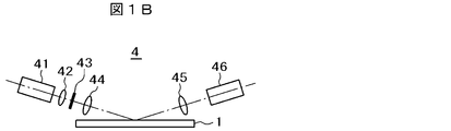
- Optical height detection system 4 as shown in FIG. 1B, a light source 41 for emitting a height measurement light, a condenser lens 42 to the height measurement light emitted from the light source for focusing light collection by the condenser lens
- a condensing lens 45 that condenses the light and a detector 46 that detects the height measurement light collected by the condensing lens and converts it into an electrical signal are provided. Information on the height measurement light converted into an electrical signal by the detector is sent to the control system 25, and the height is calculated.
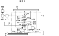
- FIG. 2A shows an example of the optical microscope 5 shown in the present embodiment.
- 2A includes a dark field illumination unit 501 capable of emitting light of one or a plurality of wavelengths, a mirror 503 for irradiating the surface of the sample 1 with illumination light emitted from the dark field illumination unit 501, and a sample.
- the sample 1 is irradiated on the sample 1 from the spatial distribution optical element 201 and the dark field illumination unit 501 to be inserted into the pupil plane 302 of the objective lens extracted in 510B.
- a beam trap 504 that collects the reflected light that has been reflected by reflection, an optical element switching mechanism 31 that switches the optical elements of the spatial distribution optical element 201 (see FIG. 9), and an image of the sample 1 imaged by the imaging lens 511 is captured.
- the position where the solid-state imaging device 509 is installed may be a conjugate position with the sample surface or the pupil plane of the objective lens and the conjugate position or near each conjugate position.
- the vacuum chamber 12 is vacuum-sealed and the windows 13A and 13B are opened. I have.
- the dark field illumination unit 501 (illustrated in FIG. 4) of the optical microscope 5, the spatial distribution optical element 201 and the spatial distribution optical element holder 32 of the optical microscope 5, and the solid-state imaging element 509 of the optical microscope 5 are connected to the control system 25. Then, the optical conditions set by the control system 25 are controlled.
- the height control mechanism 11 is connected to the control system 25, and the solid-state image sensor 509 is connected to the image processing unit 411.
- the lenses 510A and 510B are used to draw out the pupil plane 302 of the objective lens 505 to the outside and form the lens 510, the imaging lens 511, and the spatial distribution optical element 201, and drive the spatial distribution optical element holder 32.
- the spatial distribution optics selected from one or a plurality of spatial distribution optical elements 201 held by the spatial distribution optical element holder 32 on the pupil plane 302 taken out of the lens 510, the imaging lens 511, and the spatial distribution optical element 201 The element 201 is inserted.
- the lenses 510A and 510B and the imaging lens 511 are a set of three, and the image of the sample 1 is formed on the detection surface of the solid-state imaging device 509.
- the lens 510 uses two lenses 510, the imaging lens 511, and the spatial distribution optical element 201.
- the number of lenses 510 may be one or more.
- the optical microscope 5 redetects the position of the defect on the sample 1 detected by the inspection apparatus 7 using the defect position information detected by the inspection apparatus 7 (
- the dark field illumination unit 501, the spatial distribution optical element 201, and the spatial distribution using the function of detecting and describing the defect detected by the inspection apparatus 7 (for example, luminance, bright spot size, scattering direction, polarization) are used.
- the height control mechanism 11 and the optical height detection system 4 have a function as a focusing means for performing sample focusing, and have a function of setting the optical element holder 32 or any one of them.
- Reference numeral 25 denotes a function as position correction means for correcting the position information of the defect based on the position information of the defect detected by the optical microscope 5, and the SEM 6 is corrected by the control system 25.
- the structure has a function of observing defects.
- the stage 3 places the sample 1 and moves between the optical microscope 5 and the SEM 6 so that defects detected by the optical microscope 5 can be observed by the SEM 6.
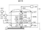
- an optical microscope 5 ′ having a function of changing the direction of illumination will be described with reference to FIG. 2B.
- the optical microscope 5 ′ having a function of changing the direction of illumination By using the optical microscope 5 ′ having a function of changing the direction of illumination, the influence of the defect direction on the detection sensitivity can be suppressed.
- the same components as those of the optical microscope 5 described in FIG. 2A is the arrangement of the dark field illumination unit 501 and the illumination method of the sample 1.
- the illumination light from the dark field illumination unit 501 is optical microscope.
- the rotating mirror 526 has a rotation axis center of the optical axis 301 of the detection optical system formed by the objective lens 505, the lenses 510A and 510B, the imaging lens 511, and the solid-state imaging device 509. As a function of rotating.
- the conical incident mirror 527 reflects the illumination light 304 reflected by the rotating mirror downward.
- the illumination light 304 reflected by the conical incident mirror 527 is reflected on the sample 1 by the conical mirror 528.
- the conical incident mirror 527 and the conical mirror 528 are annular conical shapes for reflecting light in the azimuth angle range from ⁇ to ⁇ , with the angle in the plane being 0 with the optical axis 301 of the detection optical system as the center.
- it may be a shape in which a part of the annular conical shape is missing.
- a halved shape may be used in which only a region having an azimuth angle of 0 to ⁇ is reflected with a certain angle being 0.
- the region from ⁇ to 0 may be a beam trap in order to trap the light reflected by the sample 1.
- the illumination light 304 passes through the optical path 304A in the figure.
- the illumination light 304 passes through the optical path 304B in the figure, and can illuminate the sample 1 with an azimuth angle different from that of the illumination light 304A.
- Light scattered on the sample 1 by irradiation with the illumination light 304A or 304B passes through the objective lens 505, the lens 510, the imaging lens 511, and the spatial distribution optical element 201 to form an image, and is disposed on the imaging surface.
- the formed optical image is picked up by the solid-state image pickup device 509.
- the rotational azimuth angle of the rotating mirror 526 is controlled by the control system 25 (FIG. 1). Further, the rotation azimuth angle of the rotating mirror 526 and the detection signal obtained by the solid-state imaging device 509 can be stored in the storage device 24 (FIG. 1).
- a beam trap may be provided on the back surface of the reflection surface that reflects the illumination light 304 of the rotating mirror 526.
- a rotating mirror 526 having a function of rotating the optical axis 301 of the detection optical system around the rotation axis and a function of changing the inclination of the reflecting surface of the rotating mirror 526 with respect to the optical axis 301 of the detection optical system, and a conical incident mirror 527
- the conical reflecting mirror 527 and the conical mirror 528 may be used, which are characterized in that the reflecting surface of the reflecting mirror and the reflecting surface of the conical mirror 528 are aspherical.
- the rotation azimuth angle of the rotating mirror 526 and the inclination of the reflecting surface of the rotating mirror 526 with respect to the optical axis 301 of the detection optical system are controlled by the control system 25 (FIG. 1). Further, information on the rotational azimuth angle of the rotating mirror 526 and the tilt of the reflecting surface of the rotating mirror 526 with respect to the optical axis 301 of the detection optical system is stored together with a detection signal obtained by capturing an optical image with the solid-state image sensor 509. It can be stored in the device 24 (FIG. 1).
- the conical incident mirror 527 and the conical mirror 528 may have a conical shape to reflect light in the region of azimuth angle ⁇ to ⁇ with the optical axis 301 of the detection optical system as the axis center and an angle of 0, or a conical shape.
- a shape lacking a part of the shape may be used.
- a halved shape may be used in which only a region having an azimuth angle of 0 to ⁇ is reflected with a certain angle being 0.
- the aspherical shapes of the conical incident mirror 527 and the conical mirror 528 may not be elliptical and parabolic.
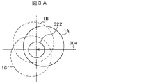
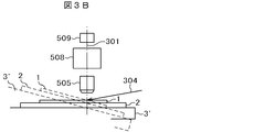
- FIG. 3A is a diagram for explaining an optical microscope using a stage equipped with a rotation and tilt function as the stage 3 ′.
- the illumination direction is fixed, but an optical microscope can be obtained by using a stage 3 ′ equipped with a rotation and tilt function. It is possible to illuminate the defect from a different illumination direction from the samples 1A, 1B, and 1C by rotating the sample 1 around the five measurement regions 322.
- FIG. 3B is a schematic view of an optical microscope that can illuminate a defect with different incident angles by using a stage 3 ′ having a function of tilting the sample 1.
- the incident direction of the illumination light 304 is fixed even if the incident direction is fixed.
- the illumination light can be varied.
- the bright field illumination unit 522 described with reference to FIGS. 2A and 2B illuminates the sample 1 along the optical axis 301 of the detection optical system with the bright field light source 506 and the light emitted from the bright field light source 506.
- a half mirror 507 is used.
- the ratio of reflection and transmission of the half mirror 507 may be arbitrary.
- a configuration is adopted in which more scattered light from the defect is guided to the lenses 510A and B, the imaging lens 511, the spatial distribution optical element 201, and the solid-state imaging element 509. Better.
- the bright field light source 506 can use a lamp or a laser.
- the illumination can be brightened and more scattered light can be guided to the solid-state imaging device 509 by replacing the half mirror 507 with a dichroic mirror.
- a mechanism (not shown) for removing the half mirror 507 from the optical axis 301 of the detection optical system may be provided. In that case, there is an advantage that more scattered light can be guided to the solid-state imaging device 509.
- the dark field illumination unit 501 shown in FIG. 4A includes an illumination light source 513 that emits, for example, a visible light laser, an ultraviolet light laser, a vacuum ultraviolet light laser, a lamp or a light emitting diode, an optical filter 514 that adjusts the intensity of illumination light, and illumination light. And a lens group 516 for focusing the illumination light on the sample 1.
- an illumination light source 513 that emits, for example, a visible light laser, an ultraviolet light laser, a vacuum ultraviolet light laser, a lamp or a light emitting diode
- an optical filter 514 that adjusts the intensity of illumination light
- illumination light and illumination light.
- a lens group 516 for focusing the illumination light on the sample 1.
- the optical filter 514 in FIG. 4A When an attenuator, ND filter, polarizer, or the like is used for the optical filter 514 in FIG. 4A, the optical filter is moved in parallel or rotated to adjust to an appropriate amount of illumination light depending on the size of the defect, or another optical filter is used. It is possible to replace or remove the optical filter.
- the wave plate 515 can change the polarization of illumination, and can be changed or taken out arbitrarily.
- the illumination light source 513 is a laser oscillator, a broadband white lamp, or a light emitting diode.
- the laser oscillator oscillates visible light (400 nm to 800 nm) having a wavelength of 405 nm, 455 nm, 488 nm, 532 nm, ultraviolet light having a wavelength of 400 nm or less, or vacuum ultraviolet light having a wavelength of 200 nm or less. Either can be used. As these selection methods, if a continuous wave laser is used, it is cheap and stable, and a small device can be realized.
- the wavelength of the illumination light source 513 is not limited to the above wavelength. A laser capable of oscillating multiple wavelengths may be used.
- the surface of the sample 1 is irradiated with a short wavelength ultraviolet laser, vacuum ultraviolet laser, or visible short wavelength blue laser to detect defects or crystal defects inside the sample.
- a short wavelength ultraviolet laser, vacuum ultraviolet laser, or visible short wavelength blue laser it is preferable to irradiate the surface of the sample 1 with a visible laser or an infrared laser.
- ultraviolet light When sensitivity for detecting defects on the surface of sample 1 or near the surface of sample 1 is required, ultraviolet light is used.
- the distributed optical element 201 becomes an ultraviolet region compatible optical element such as synthetic quartz or a reflective optical element. If further sensitivity is required, vacuum ultraviolet light is used.
- the objective lens 505, the vacuum sealing window 13B, the half mirror 507, the lens 510, the imaging lens 511, and the spatial distribution optical element 201 are vacuum ultraviolet light such as fused silica.
- the entire optical path in the optical microscope 5 is placed in a vacuum or in a nitrogen gas atmosphere, for example, to prevent vacuum ultraviolet rays from being absorbed along with propagation. Since the purpose is to propagate vacuum ultraviolet rays, the gas to be filled is not limited to nitrogen.
- P-polarized laser light is used for irradiation of the sample 1
- S-polarized laser light is used when the surface of the sample 1 is covered with a metal thin film.
- P-polarized light or S-polarized linearly polarized light is used for more efficiently observing scattered light and realizing observation with good S / N.
- P-polarized illumination is suitable because S-polarized light has poor scattering ability and the amount of absolute scattered light decreases, resulting in poor efficiency.
- the P-polarized illumination is used, the scattered light from the substrate becomes strong, and minute defects or minute foreign objects cannot be observed, so that the S-polarized illumination is suitable.
- the dark field illumination unit 501 in FIG. 4B has illumination intensities of two illumination light sources 513A and 513B and illumination lights 304A and 304B of different wavelengths emitted from the illumination light sources so that illumination with two different wavelengths is possible.
- the lens groups 516A and 516B are arranged in the optical paths of the illumination lights 304A and 304B so that the two illumination lights 304A and 304B are focused on the sample 1, respectively, and the surface of the sample 1 is simultaneously irradiated with two different wavelengths of illumination light. It can be illuminated.
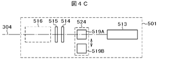
- the dark field illumination unit 501 in FIG. 4C includes a nonlinear optical crystal switching mechanism 524 that converts the nonlinear optical crystals 519A and 519B that convert the wavelength of the illumination light 304 emitted from the illumination light source 513 so that illumination with two different wavelengths can be performed.
- the illumination light 304 can be converted into a different wavelength by being used in and out of the optical path of the illumination light source 513, and the surface of the sample 1 can be illuminated with two different wavelengths.
- a long wavelength laser may be used as the illumination light source 513 and converted to a second harmonic, a third harmonic, a fourth harmonic, or the like using a nonlinear optical crystal 519, and the surface of the sample 1 may be irradiated with the short wavelength illumination light 304. .
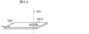
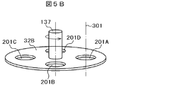
- FIG. 5A and 5B show an example of the spatial distribution optical element holder 32.
- FIG. 5A a plurality of spatial distribution optical elements 201 having different characteristics are held in the spatial distribution optical element 201 by the spatial distribution optical element holder 32 (in the example shown in FIG. 5A, the spatial distribution optical element holder 32A has a spatial distribution).
- the spatial distribution optical element holder 32B includes four types of spatial distribution optical elements 201A to 201D.
- the spatial distribution optical elements 201A to 201D on the pupil plane 302 of the objective lens 505 It is set as the structure which can be switched and inserted in either. Further, the spatial distribution optical elements 201A to 201D may not be arranged on the optical axis 301 of the detection optical system.
- the spatial distribution optical element 201 inserted into the pupil plane 302 of the objective lens 505 is moved in and out on the optical axis 301 of the detection optical system. And has a function of switching the presence or absence of the spatial distribution optical element 201.
- the spatial distribution optical element holder 32A of FIG. 5A the case where there is one spatial distribution optical element 201 is shown, but a plurality of spatial distribution optical elements 201 may be provided.
- the switching mechanism includes a spatial distribution optical element holder 32B in which a plurality of distributed polarization elements 201A to 201D having different characteristics are arranged, and a rotation driving unit 137 for rotating the spatial distribution optical element holder 32B.
- the spatial distribution optical element holder 32B is a mechanism for switching to any one of the plurality of spatial distribution optical elements 201A to 201D according to the type of minute defect to be detected.
- the spatial distribution optical element holder 32 shown in FIGS. 5A and 5B is a position of the spatial distribution optical element holder 32 in order to avoid disturbing an acquired image when performing bright field observation or not using the spatial distribution optical element. Is observed at a place where the spatial distribution optical element 201 is not installed. Or, switch to place the spatial distribution optical element 201 to the spatial distribution optical element holder 32 is installed parallel plate glass of the same thickness. The reason why the parallel flat glass having the same thickness as the spatial distribution optical element 201 is installed is to prevent the optical path length from changing when the spatial distribution optical element 201 is removed to prevent the image of the sample 1 from being formed on the solid-state imaging element 509. Because. Alternatively, a mechanism for adjusting the position of the imaging lens 511 for forming an image or the solid-state image sensor 509 and forming an image on the solid-state image sensor 509 without using parallel flat glass may be used.
- the spatial distribution optical element 201 is an optical element that can increase the ratio of scattered light from a foreign substance to scattered light from the substrate surface and enables detection of a defect with high S / N.
- the spatial distribution optical element 201 is configured by any one or a combination of a spatial filter, a phase shifter, an optical filter (ND filter), a color filter, a wave plate, a polarizing plate, a liquid crystal, a magneto-optic modulator, and a photonic crystal, and a foreign object.
- the filter has a function of transmitting scattered light under optical conditions (wavelength, transmittance, polarized light, phase difference) and controlling the polarization direction with a large ratio of scattered light from the substrate surface to scattered light from the substrate.
- Either or both of the spatial distribution optical element 201 and the spatial distribution optical element holder 32 are connected to the control system 25 and can select or control optical conditions.
- the sample 1 is illuminated with a laser as the illumination light 312 obliquely from above, and the light scattered from the minute foreign matter or minute defect placed on the sample 1 is the optical element closest to the sample 1 of the detection optical system.
- the closest surface (pupil plane 302) to the sample 1 is that to calculate the polarization distribution with the intensity distribution of the scattered light.
- FIG. 6 shows an example of the scattered light intensity distribution of the anisotropic defect obtained by the scattered light simulation.
- the scattered light intensity distribution and the polarization distribution differ depending on the inclination 303 of the defect with respect to the illumination light. Therefore, even if the defects have the same size due to the defect inclination 303 with respect to the incident light, the sensitivity varies.
- FIGS. 6 (e) to (h) show examples of the scattered light intensity distribution of the defect for each incident angle of illumination. These distributions are obtained by a scattered light simulation. Note that the scattered light intensity distribution to be obtained is not limited to these, and may be described using a polarization component.
- the polarization component may be radial polarization, azimuth polarization, linear polarization with the polarization angle inclined in the range of ⁇ to ⁇ , or elliptical (circular) polarization.
- Each scattered light intensity distribution is scattered light simulation result of the calculation models of the left Figures 6 (a) ⁇ (d).
- the region 308 is a region where the scattered light intensity is strong
- the region 309 is a region where the scattered light intensity is slightly strong
- the region 310 is a region where the scattered light intensity is slightly weak
- Reference numeral 311 denotes a region where the scattered light intensity is weak, but these indicate the relative relationships of the intensities in the same distribution, and do not necessarily indicate the same intensity even in the same region between the distributions (for example, FIG.
- the region 308 in the scattered light intensity distribution diagram at the angle 303a of 6 ⁇ (e) and the region 308 in the scattered light intensity distribution diagram at the angle 303b of Fig. 6 (f) do not necessarily show the same intensity).
- the scattered light from the defect is strongly scattered forward when the defect has no or very small inclination with respect to the incident angle of illumination.
- region the inclination of the defect with respect to the incident angle of the illumination is scattered strongly accordance large it can be seen that moves to the side.
- the upward scattered light component tends to increase.
- the ratio of the scattered light from the substrate surface to the scattered light from the foreign material can be increased by rotating the sample 1 or appropriately setting and arranging a polarizing filter, or combining them, and a high S / N defect Detection is possible.
- the defects for which the scattered light intensity distribution is obtained are not limited to these, and may be a defect shape to be detected such as a spherical defect, a polishing defect, a stacking fall, a scratch, a foreign substance in a film, or a crystal-induced defect.
- the intensity distribution for each polarization of each defect and the intensity distribution for each polarization component of the scattered light intensity from each defect may be used.
- the required polarized light is not limited to these, and may be linearly polarized light whose polarization angle is in the range of ⁇ to ⁇ , or may be elliptical (circular) polarized light.
- the scattered light intensity distribution and the polarization distribution are different depending on the type, shape, and direction of the defect in the optical characteristics of the scattered light. For this reason, it is necessary to select an illumination condition and a detection condition suitable for the defect shape and defect direction for high sensitivity detection.
- the illumination condition the illumination wavelength, the incident azimuth angle and elevation angle of the illumination, the intensity, and the like can be considered.
- the vibration direction of light that is, the polarization direction
- the scattered light from the sample 1 can be suppressed or the scattered light from the defect can be amplified. Therefore, a substrate for scattered light from a foreign object can be obtained by appropriately setting and arranging an optical rotator on or near the pupil plane 302 of the optical microscope 5 ′ shown in FIG. 2A or the optical microscope 5 ′ shown in FIG. 2B.
- the ratio of scattered light from the surface can be increased, and a high S / N defect can be detected.
- each of the plurality of polarization direction control devices constituting the spatial distribution optical element 201 can control the optical rotation angle, and can adjust the optical rotation angle in time according to the scattered light distribution.
- the liquid crystal is an intermediate state between the liquid and the crystal, and is a crystal having both the fluidity of the liquid and the anisotropy of the crystal, and the liquid crystal has no chirality with the optical rotatory liquid crystal having the chirality.
- the liquid crystal molecules in contact with the substrate are arranged by rotating the liquid crystal molecules in the vertical direction. The direction of rotation is determined by the chirality of the liquid crystal.
- the horizontally aligned liquid crystal molecules rise vertically. As the liquid crystal molecules stand up, the optical rotation is lost.
- the polarization direction can be changed by controlling the rising angle of the liquid crystal molecules according to the magnitude of the applied voltage.
- a spatial distribution optical element using a liquid crystal that performs rubbing on the alignment film, controls the alignment of liquid crystal molecules in the liquid crystal by applying a voltage, and controls the polarization direction will be described.
- the liquid crystal When there is no applied voltage, the liquid crystal is aligned along the rubbing direction of the alignment film, and the alignment of the liquid crystal molecules in the liquid crystal is not rotated but is parallel between the alignment film and the outermost layer.
- a voltage is applied between the electrodes, the liquid crystal molecules in the vicinity of the electrodes rotate in the plane, but the liquid crystal molecules in the vicinity of the alignment film are aligned along the rubbing direction.
- the polarization direction of the liquid crystal molecules and thus the polarization direction of the light is rotated, and the polarization state can be changed.
- the polarization direction can be changed by controlling the swivel angle of the liquid crystal molecules in the plane parallel to the alignment film according to the magnitude of the applied voltage.
- the spatial distribution optical element 201 which has arrange
- the polarization direction is controlled using Faraday rotation by controlling the magnetization direction of the transparent magnetic body 222 sandwiched between two transparent substrates.
- the magnetization direction is controlled by applying an external magnetic field, applying stress to the crystal by a piezoelectric actuator, or applying an electric field, applying an external magnetic field, and applying stress to the crystal by a piezoelectric actuator.
- optical rotation is not required, such as during bright field observation, optical rotation can be easily removed by applying no stress, no electric field, or no external magnetic field.
- the sample 1 is transferred onto the sample holder 2 in the vacuum trough 12 through a load lock chamber (not shown). Then, the sample 1 is moved into the field of view of the optical microscope 5 or 5 ′ under the control of the stage 3. At this time, there is a possibility that the sample 1 is deviated from the focal position of the optical microscope.
- the objective lens 505 and the mirror 503 are moved to Z (height) using the height control mechanism 11 so that the sample 1 is set at the focal position of the optical microscope 5. Move in the direction. A method of determining the amount of movement in the Z direction will be described later.
- Wafer alignment is performed to match the reference position of the sample 1 with the reference of the stage 3 (step S6001).
- This wafer alignment is performed using a bright field observation image detected by the optical microscope 5 or 5 ′ shown in FIG. 2A or B.
- illumination light is emitted from the bright field illumination 506, reflected by the half mirror 507 disposed on the optical axis 301 of the detection optical system, and irradiated onto the sample 1 using the objective lens 505.
- the reflected light from the sample 1 passes through the lens 510, the imaging lens 511, and the spatial distribution optical element 201 and is imaged on the solid-state imaging element 509.
- the bright field light source 506 is, for example, a lamp.
- the spatial distribution optical element 201 inserted on the optical axis 301 of the detection optical system is switched to a parallel plate glass having the same thickness.
- the stage 3 is moved so that the defect to be observed on the sample 1 enters the field of view of the optical microscope 5 or 5 ′ using the positional information of the defect detected in advance by another inspection apparatus 7 and stored in the storage device 24.
- Move (step S6002) the height control mechanism 11 moves the objective lens 505 to perform focusing (step S6003).
- the optical condition the control system 25 has been set (step S6004).
- This optical condition includes illumination conditions consisting of any one of the illumination wavelength, illumination incident angle, illumination azimuth angle, illumination intensity, illumination polarization, or a combination thereof, and the sensitivity (gain) of the solid-state imaging device 509, accumulation time, and spatial distribution optics.
- the control system 25 selects the optical condition of the optical microscope 5 or 5 'from the inspection information of the sample 1 output by the other inspection device 7 (step S6012).
- the inspection information of the sample 1 output from the other inspection apparatus 7 includes any of defect coordinates, defect signal, defect shape, polarization of defect scattered light, defect type, defect label, defect feature, and scattering signal of the sample 1 surface. Or the inspection result composed of a combination of these, and the illumination incident angle, illumination wavelength, illumination azimuth angle, illumination intensity, illumination polarization, detector azimuth angle, detector elevation angle, detector detection area It is inspection information configured by an inspection condition configured by any one or a combination thereof.
- the inspection information of the sample 1 output for each sensor or the inspection information of the sample 1 obtained by integrating a plurality of sensor outputs is used.
- the image processing unit 411 searches for a defect from the images acquired by the optical microscope 5 or 5 ′ and the solid-state imaging device 509 (step S6005), and when a defect is detected (step S6006-YES), the optical microscope 5 or 5 Let's observe this defect with the SEM 6 using the position information of the defect previously detected by the other defect inspection apparatus 7 from the difference between the defect detection position by 'and the position information of the defect previously detected by the other defect inspection apparatus 7
- the deviation amount of the visual field position of the SEM 6 with respect to the defect is calculated (step S6007). Based on the calculated deviation amount, the position information of the defect detected in advance by the other defect inspection apparatus 7 is corrected (step S6008), and the stage 3 is moved based on the corrected position information.
- the defect whose information is corrected is moved to the field of view of the SEM 6, and the defect is observed with the SEM 6 (step S6009).
- information on the observed defects is sent to the control system 25, and processing such as display on the user interface 23, registration in the database 22, and automatic defect classification is performed.
- FIG. 7B the processing from S6001 to S6007 is the same as that described in FIG. 7A.
- FIG. 7B shows a processing flow when there are many defects to be observed.
- some representative points are extracted, and the processing from steps S6001 to S6007 is sequentially repeated for each of the extracted defects in the same manner as described with reference to FIG. 7A.
- each of the defects detected by the other defect inspection apparatus 7 in advance is determined from the difference between the position information of the defect previously detected by the other defect inspection apparatus 7 and the defect detection position by the optical microscope 5 or 5 ′.
- a deviation amount of the visual field position of the SEM 6 with respect to the defect when the defect on the sample 1 is to be observed with the SEM 6 is calculated (step S6007).
- step S6108 When the amount of deviation between the defect position detected by the inspection apparatus 7 and the SEM visual field position is obtained for all the extracted defects (YES in step S6108), information on the obtained deviation amount is then obtained in step S6109.
- the positional information obtained by detecting in advance by another defect inspection apparatus 7 is also corrected for defects that have not been detected by the optical microscope 5 or 5 ′ other than the representative few points.
- step S6110 the stage 3 is based on the corrected position information. To move the defect to the field of view of the SEM 6 and sequentially observe a large number of defects to be observed with the SEM 6, and information on the observed defects is sent to the control system 25 for display on the user interface 23 and the database 22. Registration, automatic defect classification, etc.
- the inspection apparatus 7 More accurate position information on the defect observation apparatus 100 of the detected defect can be obtained.
- the position of the stage 3 can be controlled so that the defect detected by the inspection apparatus 7 can be surely entered into the field of view of the SEM, so that the optical conditions of the optical microscope of the conventional defect observation apparatus are fixed.
- the throughput in the case of observing defects with the defect observation apparatus 100 can be improved.
- step S6006-NO If a defect cannot be detected by the above-described defect detection procedure (step S6006-NO), it is considered that the defect is outside the field of view of the optical microscope 5, and therefore, the periphery of the field of view of the optical microscope 5 is searched. Also good.
- searching for the peripheral portion step S6014-YES
- the amount corresponding to the visual field of the sample 1 moves (step S6013), performs the processing from the above defect detection procedure (Step S6005). If no peripheral search is performed (step S6014—NO), the process proceeds according to the procedure.
- an optical filter 514 having an appropriate density is set to adjust the illumination intensity of the optical microscope 5 or 5 ′ based on the luminance information obtained by the other inspection apparatus 7, or the dark field illumination light source 513 has an illumination intensity.
- the illumination intensity according to the size of the defect can be set at high speed. Therefore, it is possible to suppress a ghost and a deterioration in coordinate accuracy that may occur in a huge defect, and it is possible to improve not only the inspection time but also the defect detection rate and the coordinate accuracy.
- the orientation and shape of the target defect can be estimated from the difference in output of each sensor. Based on this estimation, it is possible to detect defects with high sensitivity by setting optical conditions such as illumination wavelength, illumination incident angle, detected polarization, and transmittance.
- FIG. 8A is an example of setting the illumination intensity proportional to the luminance of the defect output by the inspection apparatus.
- Output data 101 of another inspection apparatus 7 is stored in the storage device 24.
- the brightness value L0 of the detected defect 571 in the stored output data 101 of the other inspection apparatus 7 is read, and the illumination intensity P0 of the dark field illumination unit 501 is set based on the brightness value L0.
- the position of the attenuator 529 placed in front of the illumination light source 513 is adjusted to change the transmittance of the attenuator so that the previously set illumination intensity P0 is obtained.
- the sample 1 can be illuminated with the illumination intensity P0 set in the processing system 25.
- FIG. 8A illustrates an example in which the illumination intensity is controlled by changing the position of the attenuator 529.
- an ND filter whose optical density changes continuously is used, and the coordinates of the ND filter are changed. It is also possible to control the illumination intensity of the dark field illumination unit 501.
- a polarizer is disposed, and the illumination intensity is reduced by rotating the polarizer disposed on the optical axis of the illumination light source 513 described above so that the illumination intensity set by the control system 25 is obtained. It can also be controlled to be P0.
- the illumination intensity control method using a polarizer changes depending on the illumination intensity for which the polarization condition is set, a half-wave plate is disposed on the illumination optical axis in order to cancel the polarization change. You can also.
- the illumination intensity may be set using the defect size information in the output data 101 of another inspection apparatus 7 instead of the luminance value.
- a detection condition setting method for the spatial distribution optical element will be described with reference to FIG. 8B.
- Output data 101 including detection values and defect coordinates of a plurality of detectors 626 (for example, in the frame 398 in FIG. 10) capable of detecting scattered light having different azimuth angles and scattering angles, and optical conditions (illumination conditions) of the inspection apparatus 7 , Detection condition) and condition data 118 of the inspection device 7 including the position information of the detector are stored in the storage device 24 (S801).
- the output data 101 and the condition data 118 stored in the storage device 24 are read out by the control system 25, and the scattering intensity distribution tendency 120 of the detection target defect is acquired (S802).
- the defect shape 121 is estimated by comparing the scattering intensity distribution tendency 120 of the target defect acquired in the control system 25 with the scattering intensity distribution tendency 112 of each defect shape stored in the library 22 (S803).
- the spatial distribution optical element 201 capable of detecting the estimated defect shape 121 with a high S / N is selected (S804).
- the driving of the spatial distribution optical element holder 32 by a drive mechanism (not shown) is controlled (S805). Thereby, the defect can be detected with high S / N by the spatial distribution optical element 201 matched to the defect type.
- the spatial distribution optical element 201 that can obtain a high S / N is selected from the scattering intensity distribution tendency of the inspection target defect created from the output information of the inspection apparatus 7 in the control system 25 without estimating the defect shape. Also good. In this case, it is necessary to consider the difference in the settable optical conditions in the inspection optical conditions of the optical microscope 5 or 5 'sample 1 in the test device 7, the correction of the optical condition setting due to the difference in optical conditions in advance library 22 A method of saving is conceivable.
- the spatial distribution optical element 201 When using in place of driving the spatial distribution optical element holder 32 by the drive mechanism, the spatial distribution optical element 201 that can change the optical properties by changing the applied voltage applied to the spatial distribution optical element 201, the control system 25 By controlling the voltage applied between the electrodes so that the optical conditions selected in (1) can be obtained, the spatial distribution optical element 201 matched to the defect can be set.
- the optical condition 119 to set the defect shape is not limited to the spatial distribution optical element 201 characteristics, it is possible to set the illumination condition and the detection condition.
- illumination conditions and detection conditions can be controlled according to the set optical conditions.
- the optical microscope 5 ′ configured to change the incident direction of illumination described with reference to FIG. 2B
- an appropriate illumination direction is selected by the control system 25 based on the defect shape estimated by the control system 25 described above.
- rotating the rotating mirror 526 and controlling the illumination azimuth it is possible to detect the defect according to the azimuth of the defect and to stabilize the detection sensitivity.
- the detector 626 of the inspection apparatus 7 may not be plural.
- a method of acquiring the scattering intensity distribution tendency using the output data 101 of the inspection apparatus acquired under different optical conditions can be considered.
- Different optical conditions include, for example, illumination direction, illumination wavelength, illumination intensity, polarization, spatial filter shape, and the like.
- the scattering intensity distribution tendency 112 for each defect shape and the appropriate optical condition data 119 for each defect shape, which are stored in the library 22 in advance, are created from the aforementioned scattered light simulation and experimental results.
- the output data 101 of the inspection apparatus 7 may include the illumination direction. At that time, if a difference in illumination direction in the defect inspection apparatus 7 to be measured is coordinate-corrected and the estimated defect shape 121 is derived, a more appropriate optical system can be set.
- a defect position correction amount calculation method for each defect using data output from the inspection apparatus 7 For each defect detected by the inspection apparatus 7, a defect position correction amount for observing with the defect observation apparatus 100 is calculated in advance and registered in the database 22, and a position correction amount for a plurality of defects or all defects is recorded. After the calculation is completed, observe with SEM6.
- the output data 101 of the inspection apparatus 7 for example, the brightness of the defect output from one or more detectors of the inspection apparatus 7, the size of the bright spot, etc.
- the control system 25 acquires the scattering intensity distribution tendency 120 to be detected (S901).
- the defect shape 121 to be detected is estimated (S902).
- the estimated coordinate deviation amount ( ⁇ x, ⁇ y) 114 of the defect shape 121 is derived (S903).
- the coordinates of the defect to be detected acquired by the optical microscope 5 are corrected using the derived coordinate shift amount ( ⁇ x, ⁇ y) (S904).
- the actual coordinate deviation amount is calculated from the detection result of the SEM 6 (S905), and is fed back to the coordinate deviation amount data 113 depending on the defect shape stored in the library 22 (S906), whereby the accuracy of the coordinate correction is obtained.
- the coordinate deviation amount data 113 depending on the defect shape stored in advance in the library 22 is created by simulation, experimental results, and actual measurement data in the SEM.
- the optical conditions that can be set may differ between the inspection apparatus 7 and the optical microscope 5 or 5 '.
- the collection area of the sensor and the illumination wavelength are likely to be different.
- the optical conditions that can be set are different, when setting the optical conditions of the optical microscope 5 or 5 ′ using the output data from the inspection apparatus 7, it is necessary to consider the influence of the difference in optical conditions with the inspection apparatus 7. .
- the output data of the inspection device 7 is read from the storage device 24 (step S6018), and the optical condition of the inspection device 7 is read from the read output data of the inspection device 7 (step S6019).
- the optical conditions of the inspection apparatus 7 include, for example, a sensor collection area (NA), illumination wavelength, illumination incident angle, illumination polarization, and detection polarization.
- measurement data is extracted from the output data of the inspection apparatus 7 (step S6020), the library is referenced, and the measurement data of the inspection apparatus 7 extracted in step S6020 under the optical conditions of the inspection apparatus 7 extracted in step S6019. From this, defect information (shape, direction, size, etc.) is estimated (step S6021), and highly sensitive optical conditions under the optical conditions that cannot be changed by the optical microscope 5 or 5 ′ are selected (step S6022). ).
- the library is created in advance from scattered light simulation and experimental results.
- the defect type classification, the defect shape estimation, and the defect direction estimation method using the difference in sensitivity of the defect type depending on the illumination azimuth will be described with reference to FIG.
- the scattered light intensity distribution from the defect varies greatly depending on the difference in defect inclination (defect direction) with respect to the incident angle of illumination.
- defect type classification, defect shape estimation, and defect direction estimation are performed.
- FIG. 6 shows that the illumination azimuth angle 304 is changed and the defect type classification, defect shape estimation, and defect direction estimation are performed from the change in the signal value from the defect.
- a defect having an isotropic scattering intensity distribution has little or no change in the signal value from the defect even when the illumination direction is switched.
- the signal value from the defect changes when the illumination direction is switched. Further, the change in the scattered light intensity distribution due to the change in the defect orientation differs depending on the defect shape.
- the defect is observed by changing the illumination azimuth, the change 341 of the feature quantity of the defect scattered light with respect to the illumination azimuth angle is acquired, and the change of the defect feature quantity due to the change of the illumination azimuth from the database stored in the library 22 in advance.
- the defect type, defect shape, and defect direction can be estimated (342).
- the selection control limits or detecting polarized light detection region using the spatial filter and polarization distribution optics 201, classified by changing the illumination direction from the change of the signal values from the defect of the defect species, estimated defect shape defect A direction estimation method can also be performed.
- spatial filters and polarization distribution optics 201 more accurate defect type, the defect shape, allows the estimation of the defect orientation. For example, if only the forward scatter is transmitted using a spatial filter, the signal value from the defect is detected by changing the illumination direction, and the signal value shows little orientation dependency, the target defect is a spherical defect. Presumed to be. If the area is limited too much by the spatial filter, the scattered light from the defect may be weak and buried in noise.
- the illumination direction switching may be a continuous angle change instead of a discrete angle change. Also, when detecting from discrete illumination orientation may select a plurality of illumination directions on the basis of the output result of the inspection apparatus.
- the defect orientation SEM optical conditions may be set based on the illumination orientation dependence of the feature quantity of the scattered light from the defect acquired by the optical microscope 5.
- the sample may be rotated or tilted in order to improve the SEM imaging conditions (FIG. 3).
- the illumination azimuth angle 304 of the optical microscope 5 is fixed, the spatial distribution optical element 201 is rotated on a horizontal plane with respect to the sample, observation results of the plurality of samples 1 are acquired, and the spatial distribution optical element 21 is rotated.
- a change in the characteristic amount of the scattered light from the defect with respect to the corner may be acquired, and the defect type, the defect shape, and the defect orientation may be estimated from the acquired characteristic amount change of the scattered light.
Landscapes
- Chemical & Material Sciences (AREA)
- Analytical Chemistry (AREA)
- Physics & Mathematics (AREA)
- Health & Medical Sciences (AREA)
- Life Sciences & Earth Sciences (AREA)
- Biochemistry (AREA)
- General Health & Medical Sciences (AREA)
- General Physics & Mathematics (AREA)
- Immunology (AREA)
- Pathology (AREA)
- Investigating Materials By The Use Of Optical Means Adapted For Particular Applications (AREA)
Abstract
SEMを用いた欠陥観察方法及びその装置において、ウェハ上の多様な欠陥を高速、高感度に欠陥を観察することを可能にするために、他の検査装置で光学的に検査して検出した試料上の欠陥の位置情報と他の検査装置の光学的な検査の条件の情報を得、他の検査装置で検出した欠陥をSEMで観察するためのテーブル上に試料を載置し、このテーブル上に載置した試料上の欠陥を光学的に検出するための検出条件を得た他の検査装置の光学的な検査条件の情報に基づいて設定し、テーブル上に載置した試料上の欠陥の中から抽出した欠陥を設定した光学的な検出条件に基づいて検出してこの抽出した欠陥のテーブル上での位置情報を得、この得た抽出した欠陥のテーブル上での位置情報に基づいて他の検査装置で検査して検出した欠陥の位置情報を修正し、この修正した欠陥の位置情報を用いてテーブル上に載置した試料上の欠陥をSEMで観察する欠陥観察方法及びその装置とした。
Description
本発明は試料表面、または試料表面、または表面近傍に存在する欠陥等を検出する機能を備えた欠陥観察方法及びその装置に関する。
例えば、半導体デバイスの製造工程では、半導体基板(ウェハ)上に異物又はショートや断線などのパターン欠陥(以下、欠陥と記述するが異物やパターン欠陥を含むものとする)が存在すると、配線の絶縁不良や短絡などの不良原因になる。また、ウェハ上に形成する回路パターンの微細化に伴い、より微細な欠陥がキャパシタの絶縁不良やゲート酸化膜などの破壊原因にもなる。これらの欠陥のうち異物は、搬送装置の可動部から発生するものや、人体から発生するもの、プロセスガスによる処理装置の内部で反応生成されたもの、薬品や材料に混入していたものなど、種々の原因により種々の状態で発生する。また、ショートや断線などのパターン欠陥は、プロセス条件の変動やプロセス装置の条件の変動などにより発生する。このため、製造工程中で発生した欠陥を検出し、欠陥の発生源をいち早く突き止め、不良の作り込みを食い止めることが半導体デバイスを量産する上で重要になる。
従来、欠陥の発生原因を追究する方法には、まず、欠陥検査装置で欠陥位置を特定し、SEM(Scanning Electron Microscope:走査型電子顕微鏡)等で該欠陥を詳細に観察及び分類し、データベースと比較して欠陥の発生原因を推定する方法があった。
ここで、欠陥検査装置とは、半導体基板の表面をレーザで照明し、欠陥からの散乱光を暗視野観察して欠陥の位置を特定する光学式欠陥検査装置や、ランプ又はレーザ、または電子線を照射して、半導体基板の明視野光学像を検出して、これを参照情報と比較することにより半導体基板上の欠陥位置を特定する光学式外観検査装置やSEM式検査装置である。この様な観察方法に関しては、特許文献1又は2に開示されている。
また、SEMで欠陥を詳細に観察する装置に関しては、特許文献3、特許文献4及び特許文献5にそれぞれ、他の検査装置で検出した試料上の欠陥の位置情報を用いてSEM式の欠陥検査装置に装着された光学顕微鏡で試料上の位置を検出して他の検査装置で検出して得た欠陥の位置情報を修正した上でSEM式の欠陥観察装置で欠陥を詳細に観察(レビュー)する方法およびその装置、並びにSEM式の欠陥観察装置で欠陥を観察するときに、試料表面の高さを光学的に検出して試料表面をSEMの焦点位置に合わせる事が記載されている。
近年のLSI製造においては、高集積化のニーズに対応した回路パターンの微細化により、ウェハ上に形成される配線パターンの幅は縮小している。一方、配線の導電率を確保するために、配線パターンの高さは高くなっている。
これに対応して、光学式欠陥検査装置も検出すべき欠陥の寸法も微細化が求められている。
このような中、光学式欠陥検査装置又は光学式外観検査装置で欠陥を検出し、検出された欠陥の座標に基づきSEMで欠陥を観察することが行われている。
光学式欠陥検査装置を用いて半導体基板表面の欠陥を検出する場合、旧式の装置、または検査のスループットを上げるために、半導体基板表面を暗視野照明するためのレーザビームが大きなスポットサイズで半導体基板表面を走査して照射している場合がある。この場合、半導体基板表面を走査するレーザビームスポットの位置から求める位置座標の精度は、大きな誤差成分を含んでしまう。
このような大きな誤差成分を含んだ欠陥の位置情報に基づいてSEMを用いて欠陥を詳細に観察しようとすると、光学式の欠陥検査装置よりも遥かに高い倍率で観察するSEMの視野の中に、観察したい欠陥が入らない場合がある。このような場合、SEMの視野内に見たい欠陥の画像を入れるために、SEMの視野内を移動させながら欠陥を探すことになるが、そのための時間がかかってしまい、SEM観察のスループットが低下する原因になってしまう。そこで、光学式欠陥検査装置又は光学式外観検査装置で検出した欠陥をSEMの視野内に入れるために、SEM式の欠陥観察装置において、光学式顕微鏡を搭載し、光学式欠陥検査装置又は光学式外観検査装置で検出した欠陥を欠陥観察装置内で高い座標精度で検出し、確実にSEMの観察視野内に入れる欠陥観察装置がある。
微細欠陥をSEM式欠陥観察装置で観察するためには、欠陥観察装置に搭載された欠陥検出用の光学式顕微鏡も微細な欠陥を検出できることが求められている。
微細な欠陥からの微弱な光を検出するために、検出光路上に検出する散乱方向や偏光や透過率を選択及び制御する機能を持つフィルタを配置することによる高感度化や照明条件や検出条件を変えた複数光学条件による欠陥観察が進められている。しかし、欠陥の検出感度は照明波長、照明方位、欠陥の形状、欠陥方位によって異なるため、欠陥形状や欠陥の方向によって異なる光学条件で欠陥検出および観察を行う必要がある。そのため、設定する光学条件が増えることにより、適切な光学条件の設定に時間が必要となり、スループットが低下する。
そこで、本発明の目的の一つは、ウェハ上の多様な欠陥を高速、高感度に欠陥を検出することが可能な光学顕微鏡を搭載した装置を用いた欠陥観察方法及びその装置を提供することにある。
また、欠陥形状によっては散乱光の強度分布に照明方位角依存性があり,照明方位角によっては欠陥観察装置に搭載されている光学顕微鏡で検出できる領域に強い散乱光が得られず、欠陥を顕在化できないという課題がある。
そこで、本発明の目的の一つは、ウェハ上の多様な欠陥、並びに欠陥方向の異なる欠陥を高感度に検出することが可能な光学顕微鏡を搭載した装置を用いた欠陥観察方法及びその装置を提供する事にある。
上記した課題を解決するために、本発明では、他の検査装置で光学的に検査して検出した試料上の欠陥の位置情報と他の検査装置の光学的な検査の条件の情報と検査の結果の情報を得、他の検査装置で検出した欠陥をSEMで観察するためのテーブル上に試料を載置し、このテーブル上に載置した試料上の欠陥を光学的に検出するための検出条件を得た他の検査装置の光学的な検査条件の情報と検査の結果の情報に基づいて設定し、テーブル上に載置した試料上の欠陥を設定した光学的な検出条件に基づいて検出して欠陥のテーブル上での位置情報を得、この得た欠陥のテーブル上での位置情報に基づいて他の検査装置で検査して検出した欠陥の位置情報を修正し、この修正した欠陥の位置情報を用いてテーブル上に載置した試料上の欠陥をSEMで観察する欠陥観察方法とした。
また、上記した課題を解決するために、本発明では、他の検査装置で光学的に検査して検出した試料上の欠陥の位置情報と他の検査装置の光学的な検査の条件の情報を得、他の検査装置で検出した欠陥をSEMで観察するためのテーブル上に試料を載置し、このテーブル上に載置した試料上の欠陥を光学的に検出するための検出条件を得た他の検査装置の光学的な検査条件の情報と検査の結果の情報に基づいて設定し、テーブル上に載置した試料上の欠陥の中から抽出した欠陥を設定した光学的な検出条件に基づいて検出してこの抽出した欠陥のテーブル上での位置情報を得、この得た抽出した欠陥のテーブル上での位置情報に基づいて他の検査装置で検査して検出した欠陥の位置情報を修正し、この修正した欠陥の位置情報を用いてテーブル上に載置した試料上の欠陥をSEMで観察する欠陥観察方法とした。
更に、上記した課題を解決するために、本発明では、欠陥観察装置を、試料を載置して移動可能なテーブル手段と、このテーブル手段に載置された試料を観察するSEM手段と、 テーブル手段に載置された試料上の欠陥を検出する光学顕微鏡手段と、他の検査装置で光学的に検査して検出した試料上の欠陥の位置情報と他の検査装置の光学的な検査の条件の情報と検査の結果の情報を記憶する欠陥情報記憶手段と、テーブルとSEMと光学顕微鏡とを制御する制御手段とを備えて構成し、制御手段は、欠陥情報記憶手段に記憶された他の検査装置で試料上の欠陥を光学的に検査して検出した光学的な検査条件の情報と検査の結果の情報に基づいて検出した欠陥を光学顕微鏡手段で検出するための検出条件を設定し、光学顕微鏡手段を制御して設定した検出条件の下で光学顕微鏡手段を用いてテーブル手段に載置した試料上の他の検査装置で検出した欠陥を検出してこの欠陥のテーブル手段上の位置情報を取得し、この取得した欠陥のテーブル手段上の位置情報に基づいて欠陥情報記憶手段に記憶された他の検査装置で検出された欠陥の位置情報を修正し、この修正した位置情報に基づいてテーブル手段を制御してSEM手段を用いて他の検査装置で検出された欠陥を撮像してこの欠陥の画像を取得するようにした。
本発明によれば光学式欠陥検出装置で検出した欠陥をSEM等で詳細に観察する場合において、観察対象の欠陥を確実かつ高速にSEM等の観察視野内に入れることができるようになり、SEM等を用いた欠陥の詳細検査のスループットをあげることができる。または、基板上の多様な欠陥を高速、高感度に検出することが可能となる。
また、検出した欠陥の分類、形状判断の精度の向上並びに欠陥検出感度の向上が可能となる。
以下、本発明の実施の形態について適宜図面を用いて詳細に説明する。
図1Aに、本発明に係る欠陥観察装置100の構成の一例を示す。
本実施形態の欠陥観察装置100は、被検査対象の試料1、この試料を搭載する試料ホルダ2、この試料ホルダ2を移動させて試料1の全面を走査電子顕微鏡6(以下SEMと記述)の下に移動可能なステージ3、試料1を詳細観察するSEM6、SEM6の焦点を試料1の表面に合わせる為の光学式高さ検出システム4、試料1の欠陥を光学的に検出して試料1上の欠陥の詳細位置情報を取得する光学顕微鏡5、SEM6と光学顕微鏡5の対物レンズ505(図2に図示)を収納する真空漕12、SEM6および光学式高さ検出システム4および光学顕微鏡5を制御する制御システム25、ユーザインターフェース23、データベース22、光学式欠陥検査装置7等の上位システムへ接続するネットワーク21、このネットワーク21を介して得られる欠陥検査装置7の外部データ等を保存し制御システム25に与える記憶装置24、を備えて構成されている。
図1Aに、本発明に係る欠陥観察装置100の構成の一例を示す。
本実施形態の欠陥観察装置100は、被検査対象の試料1、この試料を搭載する試料ホルダ2、この試料ホルダ2を移動させて試料1の全面を走査電子顕微鏡6(以下SEMと記述)の下に移動可能なステージ3、試料1を詳細観察するSEM6、SEM6の焦点を試料1の表面に合わせる為の光学式高さ検出システム4、試料1の欠陥を光学的に検出して試料1上の欠陥の詳細位置情報を取得する光学顕微鏡5、SEM6と光学顕微鏡5の対物レンズ505(図2に図示)を収納する真空漕12、SEM6および光学式高さ検出システム4および光学顕微鏡5を制御する制御システム25、ユーザインターフェース23、データベース22、光学式欠陥検査装置7等の上位システムへ接続するネットワーク21、このネットワーク21を介して得られる欠陥検査装置7の外部データ等を保存し制御システム25に与える記憶装置24、を備えて構成されている。
欠陥観察装置100は、さらに、ステージ3、光学式高さ検出システム4、SEM6、ユーザインターフェース23、データベース22、記憶装置24、光学顕微鏡5は制御システム25と接続され、制御システム25はネットワーク21を介して上位のシステム(例えば、検査装置7)と接続されている。
光学式高さ検出システム4は、図1Bに示すように、高さ測定光を出射する光源41、光源より出射された高さ測定光を集光する集光レンズ42、集光レンズで集光された光で照明されるスリット43、高さ測定光としてスリットを透過した光の像(スリットの像)を試料1の表面に結像させる結像レンズ44、試料1で反射してきた高さ測定光を集光する集光レンズ45、集光レンズで集光された高さ測定光を検出して電気信号へ変換する検出器46を備えて構成されている。検出器で電気信号へ変換された高さ測定光の情報は制御システム25へ送られ高さが算出される。
以下、各部の詳細を図2~図5を用いて説明する。
図2Aは、本実施例で示す光学顕微鏡5の一例を示す。
図2Aの光学顕微鏡5は、一つもしくは複数波長の光を出射可能な暗視野照明ユニット501、暗視野照明ユニット501より出射される照明光を、試料1表面に照射するためのミラー503、試料1からの散乱光を捕集するまたは明視野観察をするための対物レンズ505、対物レンズの高さを調整する高さ制御機構11、試料1を明視野観察するための明視野照明光源506及び明視野照明光源506の光を試料上に照射するためのハーフミラー507、対物レンズ505の瞳面302を取り出すレンズ510A、510B、試料1の像を結像させる結像レンズ511と、レンズ510A、510Bで取り出された対物レンズの瞳面302に挿入する空間分布光学素子201、暗視野照明ユニット501から試料1に照射され試料1上で直接反射した反射光を捕集するビームトラップ504、空間分布光学素子201の光学素子を切り替える光学素子切り替え機構31(図9参照)、結像レンズ511で結像された試料1の像を撮像する固体撮像素子509、固体撮像素子509で取得した画像を処理する画像処理部411、固体撮像素子509で取得した画像を表示する画像表示部412、固体撮像素子509で取得した画像を保存する画像保存部413を備えて構成される。固体撮像素子509が設置される位置は、試料表面と共役位置もしくは対物レンズの瞳面と共役位置もしくはそれぞれの共役位置近傍でもよい。
図2Aは、本実施例で示す光学顕微鏡5の一例を示す。
図2Aの光学顕微鏡5は、一つもしくは複数波長の光を出射可能な暗視野照明ユニット501、暗視野照明ユニット501より出射される照明光を、試料1表面に照射するためのミラー503、試料1からの散乱光を捕集するまたは明視野観察をするための対物レンズ505、対物レンズの高さを調整する高さ制御機構11、試料1を明視野観察するための明視野照明光源506及び明視野照明光源506の光を試料上に照射するためのハーフミラー507、対物レンズ505の瞳面302を取り出すレンズ510A、510B、試料1の像を結像させる結像レンズ511と、レンズ510A、510Bで取り出された対物レンズの瞳面302に挿入する空間分布光学素子201、暗視野照明ユニット501から試料1に照射され試料1上で直接反射した反射光を捕集するビームトラップ504、空間分布光学素子201の光学素子を切り替える光学素子切り替え機構31(図9参照)、結像レンズ511で結像された試料1の像を撮像する固体撮像素子509、固体撮像素子509で取得した画像を処理する画像処理部411、固体撮像素子509で取得した画像を表示する画像表示部412、固体撮像素子509で取得した画像を保存する画像保存部413を備えて構成される。固体撮像素子509が設置される位置は、試料表面と共役位置もしくは対物レンズの瞳面と共役位置もしくはそれぞれの共役位置近傍でもよい。
また、光学顕微鏡5の暗視野照明ユニット501から照明される光及び試料1表面及びその近傍で散乱される光が真空槽12外へ透過するために真空槽12は真空封し窓13A、13Bを備えている。
また、光学顕微鏡5の暗視野照明ユニット501(図4に図示)及び光学顕微鏡5の空間分布光学素子201及び空間分布光学素子ホルダ32、および光学顕微鏡5の固体撮像素子509は制御システム25に接続され、制御システム25で設定した光学条件となるよう制御される。また、高さ制御機構11は制御システム25と、固体撮像素子509は画像処理部411と接続されている。
レンズ510A、510Bは対物レンズ505の瞳面302を外部へ引き出してレンズ510、結像レンズ511、空間分布光学素子201の内部に形成する為に用い、空間分布光学素子ホルダ32を駆動して、レンズ510、結像レンズ511、空間分布光学素子201の内部に取り出した瞳面302上に空間分布光学素子ホルダ32で保持する一つもしく複数の空間分布光学素子201の中から選択した空間分布光学素子201を挿入する。
本実施例においては、レンズ510A、510Bと結像レンズ511は3個1組で、試料1の像を固体撮像素子509の検出面上へ結像させる。本実施例においては、レンズ510を2枚使用するレンズ510、結像レンズ511、空間分布光学素子201になっているがレンズ510は1枚もしくは2枚以上でも良い。
以上のように構成される欠陥観察装置100において、特に、光学顕微鏡5は検査装置7で検出された試料1上の欠陥の位置を検査装置7で検出した欠陥の位置情報を用いて再検出(以下検出と記述)する機能と検査装置7で検出した欠陥の情報(例えば、輝度、輝点の大きさ、散乱方向、偏光)を用いて暗視野照明ユニット501と空間分布光学素子201と空間分布光学素子ホルダ32の設定もしくはそのいずれかの設定を行う機能を有し、高さ制御機構11と光学式高さ検出システム4は試料焦点合わせを行う焦点合わせ手段としての機能を有し、制御システム25は光学顕微鏡5で検出された欠陥の位置情報に基づいて欠陥の位置情報を補正する位置補正手段としての機能を有し、SEM6は制御システム25で位置情報を補正された欠陥を観察する機能を有する構成となっている。ステージ3は、試料1を載置して、光学顕微鏡5で検出した欠陥がSEM6で観察できるように、光学顕微鏡5とSEM6との間を移動する。
次に、照明の方位を可変にする機能を持つ光学顕微鏡5’について図2Bを用いて説明する。
照明の方位を可変にする機能を有する光学顕微鏡5’を用いることで、検出感度に対する欠陥方向の影響を抑制できる。
照明の方位を可変にする機能を有する光学顕微鏡5’を用いることで、検出感度に対する欠陥方向の影響を抑制できる。
図2Bに示した光学顕微鏡5’の構成において、図2Aで説明した光学顕微鏡5の構成と同じものについては同じ番号を付してある。図2Aで説明した光学顕微鏡5の構成と異なる点は、暗視野照明ユニット501の配置と試料1の照明方法である。図2Bに示した構成においては、暗視野照明ユニット501を用いて複数の方位角方向から切替えて試料1を暗視野照明できるようにするために、暗視野照明ユニット501からの照明光を光学顕微鏡5’の上方から導入して光路切替用の回転ミラー526を用いて光路を304A又は304Bに切替え、円錐落射ミラー527で反射させて真空封止窓13A又は13Cを透過させて真空槽12の内部に導入し、真空槽12の内部で円錐ミラー528で反射させて試料1を斜方照明する。
図2Bに示した光学顕微鏡5’において、回転ミラー526は、対物レンズ505とレンズ510A,510B、結像レンズ511及び固体撮像素子509で形成される検出光学系の光軸301を回転の軸中心として回転する機能を有する。円錐落射ミラー527は回転ミラーで反射された照明光304を下方へ落射する。円錐落射ミラー527で反射された照明光304を円錐ミラー528で試料1上へ反射させる。円錐落射ミラー527及び円錐ミラー528は、検出光学系の光軸301を軸中心に、平面内である角度を0として、方位角-πからπの領域の光を反射するために環状の円錐形状でもよいし、環状の円錐形状の一部が欠けた形状でもよい。例えば、ある角度を0として方位角0からπの領域のみを反射する、半割り形状でもよい。半割り形状の場合、試料1で反射された光をトラップするために-πから0の領域をビームトラップにしてもよい。回転ミラー526が、実線で示した位置に存在するとき、照明光304は図中の304Aの光路を通る。一方、回転ミラー526が、点線で示した位置に存在するとき、照明光304は図中の304Bの光路を通り、照明光304Aとは異なる方位角で試料1を照明することができる。
図2Bに示した光学顕微鏡5’において、回転ミラー526は、対物レンズ505とレンズ510A,510B、結像レンズ511及び固体撮像素子509で形成される検出光学系の光軸301を回転の軸中心として回転する機能を有する。円錐落射ミラー527は回転ミラーで反射された照明光304を下方へ落射する。円錐落射ミラー527で反射された照明光304を円錐ミラー528で試料1上へ反射させる。円錐落射ミラー527及び円錐ミラー528は、検出光学系の光軸301を軸中心に、平面内である角度を0として、方位角-πからπの領域の光を反射するために環状の円錐形状でもよいし、環状の円錐形状の一部が欠けた形状でもよい。例えば、ある角度を0として方位角0からπの領域のみを反射する、半割り形状でもよい。半割り形状の場合、試料1で反射された光をトラップするために-πから0の領域をビームトラップにしてもよい。回転ミラー526が、実線で示した位置に存在するとき、照明光304は図中の304Aの光路を通る。一方、回転ミラー526が、点線で示した位置に存在するとき、照明光304は図中の304Bの光路を通り、照明光304Aとは異なる方位角で試料1を照明することができる。
照明光304A又は304Bの照射により試料1上で散乱された光は、対物レンズ505、レンズ510、結像レンズ511、空間分布光学素子201を透過して結像し、結像面上に配置された固体撮像素子509によりこの結像した光学像が撮像される。回転ミラー526の回転方位角は、制御システム25(図1)で制御される。また、回転ミラー526の回転方位角及び固体撮像素子509で得られた検出信号は記憶装置24(図1)に保存することができる。また、試料1上で反射された0次光(正反射光)をトラップするために、回転ミラー526の照明光304を反射する反射面の裏面にビームトラップを設置してもよい。
また、検出光学系の光軸301を回転軸中心に回転する機能、及び検出光学系の光軸301に対する回転ミラー526の反射面の傾きを可変する機能を有する回転ミラー526と、円錐落射ミラー527の反射面及び円錐ミラー528の反射面は非球面形状になっていることを特徴とする円錐落射ミラー527及び円錐ミラー528を使用してもよい。回転ミラー526の回転方位角および検出光学系の光軸301に対する回転ミラー526の反射面の傾きを変えることで、光学顕微鏡5は、異なる方位角及び入射角で試料1を照明することが可能となる。例えば、円錐落射ミラー527の反射面は楕円形状、円錐ミラー528は放物面形状の時、円錐落射ミラー527の楕円形状の1つの焦点と、円錐ミラー528の放物面の1つの焦点は同一の点となるように配置するとよい。
回転ミラー526の回転方位角及び検出光学系の光軸301に対する回転ミラー526の反射面の傾きは、制御システム25(図1)で制御される。また、回転ミラー526の回転方位角及び検出光学系の光軸301に対する回転ミラー526の反射面の傾きの情報は、固体撮像素子509で光学像を撮像して得られた検出信号と一緒に記憶装置24(図1)に保存することができる。円錐落射ミラー527及び円錐ミラー528は、検出光学系の光軸301を軸中心に、ある角度を0として、方位角-πからπの領域の光を反射するために円錐形状でもよいし、円錐形状の一部が欠けた形状でもよい。例えば、ある角度を0として方位角0からπの領域のみを反射する、半割り形状でもよい。また、円錐落射ミラー527及び円錐ミラー528の非球面形状は、楕円形状と放物面でなくてもよい。
次に、図2Bで説明した回転ミラー526を使用せずに試料1に対する照明方向を変更する方法について図3A及びBを用い説明する。図3Aは、ステージ3’として回転及びチルト機能を搭載したステージを用いた光学顕微鏡について説明する図である。照明光304に対する欠陥の傾き303(図6参照)の違いによる感度のバラつきを抑制するために、照明の方位は固定であるが、回転及びチルト機能を搭載したステージ3’を用いることで光学顕微鏡5の計測領域322を中心に試料1を回転させ、試料1A、1B、1Cと異なる照明方向から欠陥を照明することが可能である。図3Bは、試料1をチルトさせる機能を有するステージ3’を使用することで、欠陥に対して異なる入射角で照明する事が可能である光学顕微鏡の概図である。
図3A及びBに示すように試料1を回転もしくは回転およびチルトさせる機能を有するステージ3’を搭載した光学顕微鏡5を使用することで、照明光304の入射方向は固定であっても、欠陥に対する照明光を可変することができる。
本実施例において、図2A及びBで説明した明視野照明ユニット522は、明視野光源506と、明視野光源506から放射される光を検出光学系の光軸301に沿って試料1を照明するために用いるハーフミラー507を備えて構成されている。ハーフミラー507の反射と透過の比率は任意でよい。ただし、明視野光源506の光強度が十分確保される場合は、欠陥からの散乱光をより多くレンズ510A及びB、結像レンズ511、空間分布光学素子201及び固体撮像素子509へ導く構成とする方がよりよい。
明視野光源506はランプ、又はレーザを用いることができる。レーザを用いる場合は、ハーフミラー507をダイクロイックミラーと交換することにより、照明を明るくし、より多くの散乱光を固体撮像素子509へ導くことができる。または、暗視野観察をする際には、ハーフミラー507を検出光学系の光軸301から外す機構(図示せず)を有してもよい。その場合はより多くの散乱光を固体撮像素子509へ導ける利点がある。
図4A~Cに、図2A及びBで説明した暗視野照明ユニット501の構成例を示す。
図4Aに示した暗視野照明ユニット501は、例えば可視光レーザや紫外光レーザや真空紫外光レーザやランプや発光ダイオードを出射する照明光源513、照明光の強度を調整する光学フィルタ514、照明光の偏光方向を調整する波長板515、照明光を試料1に絞るレンズ群516を備えて構成される。
図4Aに示した暗視野照明ユニット501は、例えば可視光レーザや紫外光レーザや真空紫外光レーザやランプや発光ダイオードを出射する照明光源513、照明光の強度を調整する光学フィルタ514、照明光の偏光方向を調整する波長板515、照明光を試料1に絞るレンズ群516を備えて構成される。
図4Aの光学フィルタ514に、アッテネータやNDフィルタ,偏光子などを使用した場合、欠陥のサイズなどによって適切な照明光量に調整するために光学フィルタを平行もしくは回転移動させる、もしくは別の光学フィルタに交換するもしくは光学フィルタを取り外すことが可能である。また、波長板515は、照明偏光を変更することができ、任意で変更もしくは出し入れ可能である。
照明光源513は、レーザ発振器もしくは広帯域白色ランプもしくは発光ダイオードである。レーザ発振器は例えば波長405nmや455nm、488nm、532nmの可視光(400nm-800nm)、または400nm以下の紫外光、または200nm以下の真空紫外光を発振するものであり、連続発振レーザやパルス発振レーザのどちらでも使用可能である。これらの選択方法としては、連続発振レーザを用いると安価で安定し、小型の装置が実現可能である。照明光源513の波長は上記の波長に限るものではない。多波長発振可能なレーザを用いてもよい。試料表面もしくは試料表面近傍の欠陥を検出するには、短波長の紫外レーザまたは真空紫外レーザまたは可視の中で短波長のブルーレーザで試料1表面を照射し、試料内部の欠陥もしくは結晶欠陥を検出するには可視レーザ、赤外レーザで試料1表面を照射するものがよい。
試料1表面もしくは試料1表面近傍の欠陥を検出する感度が必要な場合は紫外光を用い、その場合は対物レンズ505、真空封し窓13B、ハーフミラー507、レンズ510、結像レンズ511、空間分布光学素子201が合成石英等の紫外領域対応光学素子または反射型光学素子となる。さらに感度が必要な場合は真空紫外光を用い、その場合は対物レンズ505、真空封し窓13B、ハーフミラー507、レンズ510、結像レンズ511、空間分布光学素子201が融解石英等の真空紫外領域対応光学素子または反射型光学素子となり、さらに光学顕微鏡5における光路全体が、真空紫外線が伝播と共に吸収されることを防ぐ為に真空中または例えば窒素ガス雰囲気中に設置される。真空紫外線を伝播させることが目的なので、充満させる気体は窒素に限らない。
試料1の照射には、試料1が鏡面試料である場合はP偏光したレーザ光を用い、試料1の表面が金属薄膜で覆われている場合はS偏光したレーザ光を用いる。P偏光又はS偏光の直線偏光を用いるのは、より散乱光を効率よく観測し、S/Nのよい観測を実現する為である。すなわち、鏡面試料を観察する場合にS偏光では散乱能が悪くなり絶対的な散乱光量が減少してしまい効率が悪くなるためにP偏光照明が適しており、一方、金属薄膜等を観測する場合にP偏光照明をすると基板よりの散乱光が強くなり微小欠陥または微小異物を観測できなくなるためにS偏光照明が適している。
図4Bの暗視野照明ユニット501は、互いに異なる2波長の照明が可能なように2つの照明光源513A、513Bと、照明光源から放射された互いに異なる波長の照明光304A、304Bそれぞれの照明強度を調整できるようにそれぞれの光路に配置された光学フィルタ514A、514Bと、2つの照明光304A、304Bそれぞれの偏向方向を調整できるように701A,701Bそれぞれの光路に配置された波長板515A、515Bと、2つの照明光304A、304Bそれぞれを試料1に絞るよう照明光304A,304Bそれぞれの光路に配置されたレンズ群516A、516Bとで構成され、互いに異なる2波長の照明光で試料1表面を同時に照明可能である。
図4Cの暗視野照明ユニット501は、互いに異なる2波長の照明が可能なように照明光源513で射出された照明光304を波長を変換する非線形光学結晶519A、519Bを非線形光学結晶切り替え機構524を用い、照明光源513の光路に出し入れすることにより照明光304を異なる波長に変換することができ、互いに異なる2波長で試料1表面を照明することが可能である。照明光源513に長波長レーザを用い、非線形光学結晶519を用い2倍高調波や3倍高調波、4倍高調波などに変換し短波長の照明光304で試料1表面に照射してもよい。
図5A及びBは空間分布光学素子ホルダ32の一例を示す。
本実施例においては、空間分布光学素子201に特性の異なる空間分布光学素子201を空間分布光学素子ホルダ32で複数保持して(図5Aに示した例では、空間分布光学素子ホルダ32Aは空間分布光学素子201の有無、図5Bに示した例では、空間分布光学素子ホルダ32Bは、空間分布光学素子201Aから201Dの4種類)対物レンズ505の瞳面302に空間分布光学素子201Aから201Dのうちの何れかに切り換えて挿入することが可能な構成としている。また、空間分布光学素子201Aから201Dは、検出光学系の光軸301上に配置しなくても良い。
本実施例においては、空間分布光学素子201に特性の異なる空間分布光学素子201を空間分布光学素子ホルダ32で複数保持して(図5Aに示した例では、空間分布光学素子ホルダ32Aは空間分布光学素子201の有無、図5Bに示した例では、空間分布光学素子ホルダ32Bは、空間分布光学素子201Aから201Dの4種類)対物レンズ505の瞳面302に空間分布光学素子201Aから201Dのうちの何れかに切り換えて挿入することが可能な構成としている。また、空間分布光学素子201Aから201Dは、検出光学系の光軸301上に配置しなくても良い。
図5Aに示すように、空間分布光学素子ホルダ32Aが矢印の方向にスライドするとことで、対物レンズ505の瞳面302に挿入された空間分布光学素子201を検出光学系の光軸301上を出し入れすることができ、空間分布光学素子201の有無を切り替える機能を有する。図5Aの空間分布光学素子ホルダ32Aでは、空間分布光学素子201が1つの場合について示しているが、空間分布光学素子201が複数であっても良い。
図5Bの空間分布光学素子ホルダ32Bは、対物レンズ505の瞳面302に挿入された空間分布光学素子201Aから202Dをレンズ510、結像レンズ511、空間分布光学素子201の光軸301上で切り替える機構を示す。切り替え機構は、特性の異なる複数の分布偏光素子201Aから201Dを配置する空間分布光学素子ホルダ32B、空間分布光学素子ホルダ32Bを軸回転させるための回転駆動部137を備えて構成される。空間分布光学素子ホルダ32Bは、検出する微小欠陥の種類に応じて複数の空間分布光学素子201Aから201Dのうちの何れかに切り替える機構である。
図5A及びBに示す空間分布光学素子ホルダ32は、明視野観察をする場合もしくは空間分布光学素子を使用しない場合には、取得画像が乱れることを回避する為に空間分布光学素子ホルダ32の位置を空間分布光学素子201が設置されていない場所に設定して観察する。又は、空間分布光学素子ホルダ32に空間分布光学素子201と同厚の平行平板ガラスを設置した場所へ切り替える。空間分布光学素子201と同厚の平行平板ガラスを設置するのは、空間分布光学素子201を外すと光路長が変化して固体撮像素子509に試料1の像が結像しなくなることを回避するためである。又は、平行平板ガラスを設置せず、像を結像させる結像レンズ511又は固体撮像素子509の位置を調整し、固体撮像素子509に結像させる機構を用いても良い。
次に、空間分布光学素子ホルダ32に装着する空間分布光学素子201について説明する。
空間分布光学素子201は、異物からの散乱光の基板表面からの散乱光に対する比を大きくすることができ、高S/Nの欠陥検出を可能とする光学素子である。空間分布光学素子201は、空間フィルタ、位相シフタ、光学フィルタ(NDフィルタ)、カラーフィルタ、波長板、偏光板、液晶、磁気光学変調子、フォトニック結晶のいずれかもしくはその組み合わせによって構成され、異物からの散乱光に対する基板表面からの散乱光の比が大きい光学条件(波長、透過率、偏光、位相差)の散乱光を透過および偏光方向制御を行う機能を有するフィルタである。
空間分布光学素子201は、異物からの散乱光の基板表面からの散乱光に対する比を大きくすることができ、高S/Nの欠陥検出を可能とする光学素子である。空間分布光学素子201は、空間フィルタ、位相シフタ、光学フィルタ(NDフィルタ)、カラーフィルタ、波長板、偏光板、液晶、磁気光学変調子、フォトニック結晶のいずれかもしくはその組み合わせによって構成され、異物からの散乱光に対する基板表面からの散乱光の比が大きい光学条件(波長、透過率、偏光、位相差)の散乱光を透過および偏光方向制御を行う機能を有するフィルタである。
空間分布光学素子201を構成する、位相シフタの配置、波長板の遅相軸の傾きと進相軸の傾き、偏光方向制御装置による旋光方向、空間フィルタにおける遮光領域、偏光子の透過偏光軸方向、減光フィルタの透過率、液晶素子への印加電圧、磁気光学変調子への印加電圧、フォトニック結晶の光学特性などの決定方法は、散乱光シミュレーション若しくは実測によって求められる散乱光強度分布を基にして決定する。
空間分布光学素子201と空間分布光学素子ホルダ32のいずれかもしくはその両方は制御システム25と接続され、光学条件を選択もしくは制御することが可能である。
散乱光シミュレーションは、試料1に斜め上方より照明光312であるレーザを照明し、試料1上に置かれた微小異物または微小欠陥より散乱された光を検出光学系の試料1に最も近い光学素子の試料1に最も近い表面(瞳面302)での、散乱光の強度分布と偏光分布を計算するというものである。
図6に散乱光シミュレーションによって求めた異方性欠陥の散乱光強度分布例を示す。図6に示すように欠陥の種類によっては照明光に対する欠陥の傾き303によって散乱光強度分布、偏光分布が異なる。そのため、入射光に対する欠陥の傾き303によって同じ大きさの欠陥であったとしても感度がばらついてしまう。もしくは、入射光に対する欠陥の傾き303によっては検出できない場合が起こりうる。そのため、図2Bに示した光学顕微鏡5’や図3A又はBに示すように照明の方位を可変にして調整可能にすることは、
欠陥の安定検出に有効である。
欠陥の安定検出に有効である。
図6(a)~(d)に、散乱光シミュレーションの欠陥の計算モデル例を示す。照明の入射方向に対して、ある欠陥330の傾き303を(a)303a、(b)303b、(c)303c、(d)303dと変化させた場合の散乱光強度分布を求める計算モデル例である。また、図6 (e)~(h)に、照明の入射角毎の欠陥の散乱光強度分布例を示す。これらの分布は、散乱光シミュレーションによって、求められる。なお、求める散乱光強度分布はこれらに限られず、偏光成分で記述しても良い。偏光成分は、ラジアル偏光でもよいし、アジマス偏光でもよいし、偏光の角度がπから-πの範囲に傾いた直線偏光でもよいし、楕円(円)偏光であってもよい。各散乱光強度分布はそれぞれ左の図6(a) ~(d)の計算モデルでの散乱光シミュレーション結果である。
図6 (e)~(h)は、照明光の入射角に対して欠陥が角度(e)303a、(f)303b、(g)303c、(h)303d傾いた場合の散乱光強度分布fSB(r,θ)を示す。また、各散乱光強度分布中の軸307は、照明の入射面を瞳面302上に対応させた軸を示す。矢印312は照明光の入射方向を、矢印313は照明光の正反射方向を、それぞれ示している。図6 (e)~(h)の各偏光の強度分布において、領域308は散乱光強度の強い領域、領域309は散乱光強度がやや強い領域、領域310は散乱光強度のやや弱い領域、領域311は散乱光強度の弱い領域を示すが、これらは同分布における強度の相対的関係を示すものであり、各分布間で同一領域であっても必ずしも同一強度を示すものではない(例えば、図6 (e)の角度303aの散乱光強度分布図中の領域308と図6 (f)の角度303bの散乱光強度分布図中の領域308とは必ずしも同一の強度を示すものではない)。
図6 (e)~(h)に示す散乱光強度分布によれば、欠陥からの散乱光は、照明の入射角に対して欠陥の傾きが無い、もしくはごく小さい場合は前方に強く散乱し、照明の入射角に対して欠陥の傾きが大きくなるに従い強く散乱する領域が側方へと移動していくことがわかる。また,上方散乱光成分が増加する傾向がみられる。
このように、同一の欠陥においても照明の入射角に対する欠陥の傾きの違いで散乱光の強度分布が異なる欠陥が存在しており、したがって、これらの結果に基づいて、照明の入射方向を変更、もしくは試料1を回転、もしくは適宜偏光フィルタを設定・配置すること、もしくはそれらを組み合わせることで異物からの散乱光に対する基板表面からの散乱光の比を大きくすることができ、高S/Nの欠陥検出が可能となる。なお、散乱光強度分布を求める欠陥はこれらに限られず、球状欠陥や研磨欠陥やスタッキングフォールやスクラッチ、膜中異物、結晶起因欠陥など検出したい欠陥形状であってよい。また、散乱光強度分布だけでなく、各欠陥の偏光毎の強度及び各欠陥からの散乱光強度の偏光成分毎の強度分布でもよい。求める偏光はこれらに限られず、偏光の角度がπから-πの範囲に傾いた直線偏光でもよいし、楕円(円)偏光であってもよい。
図6に一例を示したように、散乱光の光学特性は、欠陥の種類、形状、方向によって散乱光強度分布及び偏光分布が異なっている。そのため、高感度検出のためには欠陥形状や欠陥方向に合った照明条件、検出条件を選択する必要がある。例えば、照明条件では、照明波長、照明の入射方位角と仰角、強度などが、検出条件では、検出波長、検出偏光、センサの感度、検出散乱角などが考えられる。
また、光の振動方向、すなわち偏光方向を変えることで、試料1からの散乱光を抑制もしくは欠陥からの散乱光を増幅することができる。そのため、図2Aに示した光学顕微鏡5又は図2Bに示した光学顕微鏡5’の瞳面302上もしくは瞳面302近傍に、適宜旋光子を設定・配置することで、異物からの散乱光に対する基板表面からの散乱光の比を大きくすることができ、高S/Nの欠陥検出が可能となる。
次に、空間分布光学素子201の構成に液晶を用いた場合の効果の一例について説明する。
液晶に印加する電圧の制御もしくは配向膜に施すラビングの方向を制御することによって、水晶の結晶を用いる1/2波長板や1/4波長板では実現不可能な緻密な偏光方向の制御が可能となる。また、偏光方向制御装置を二次元状に複数個配置し、1つの空間分布光学素子201として用いても良い。その際、空間分布光学素子201を構成する複数個の偏光方向制御装置は、それぞれで旋光角を制御することができ、散乱光分布に応じて旋光角を適時調整することが可能である。
液晶に印加する電圧の制御もしくは配向膜に施すラビングの方向を制御することによって、水晶の結晶を用いる1/2波長板や1/4波長板では実現不可能な緻密な偏光方向の制御が可能となる。また、偏光方向制御装置を二次元状に複数個配置し、1つの空間分布光学素子201として用いても良い。その際、空間分布光学素子201を構成する複数個の偏光方向制御装置は、それぞれで旋光角を制御することができ、散乱光分布に応じて旋光角を適時調整することが可能である。
ここで、液晶とは、液体と結晶の中間の状態であり、液体の流動性と結晶の異方性を併せ持った結晶であって、液晶にはキラリティを持つ旋光性のある液晶とキラリティの無い旋光性の無い液晶がある。
キラリティを持つ液晶の場合、基板に接している液晶分子は、垂直方向に液晶分子が旋回して並んでいる。回転の方向は、液晶のキラリティによって決まる。この液晶に光を透過させると、液晶分子のならびに従って光の偏光方向が旋回し、偏光状態を変えることができる。このキラリティを持つ液晶に電源を用い電圧を印加すると、水平に並んでいた液晶分子が垂直に立ち上がる。液晶分子が立ち上がるにつれて旋光性が失われていく。この液晶分子の立ち上がりの角度を印加電圧の大きさによって制御することで偏光方向を変えることができる。
キラリティを持つ液晶の場合、基板に接している液晶分子は、垂直方向に液晶分子が旋回して並んでいる。回転の方向は、液晶のキラリティによって決まる。この液晶に光を透過させると、液晶分子のならびに従って光の偏光方向が旋回し、偏光状態を変えることができる。このキラリティを持つ液晶に電源を用い電圧を印加すると、水平に並んでいた液晶分子が垂直に立ち上がる。液晶分子が立ち上がるにつれて旋光性が失われていく。この液晶分子の立ち上がりの角度を印加電圧の大きさによって制御することで偏光方向を変えることができる。
また、配向膜にラビングを施し、電圧印加により液晶中の液晶分子の並びを制御し、偏光方向の制御を行う液晶を用いた空間分布光学素子について説明する。
印加電圧がない場合、液晶は配向膜のラビング方向に沿って並び、配向膜-最外層間で液晶中の液晶分子の並びは旋回せずに平行である。電極間に電圧を印加すると、電極近傍の液晶分子が面内で旋回するが、配向膜近傍の液晶分子はラビング方向に沿って並んでいるため、液晶中で液晶分子の並びが旋回し、この状態の液晶に光を透過させると、液晶分子のならびに従って光の偏光方向が旋回し、偏光状態を変えることができる。配向膜に平行な面内での液晶分子の旋回角度を印加電圧の大きさによって制御することで偏光方向を変えることができる。
次に、空間分布光学素子201の構成に磁気光学効果を利用した偏光制御装置を用いた場合の効果の一例について説明する。磁気光学効果を利用した透明磁性体を用いた偏光方向制御装置を配置した空間分布光学素子201の例を示す。本例では、2枚の透明基板間に挟まれた透明磁性体222の磁化方向を制御することにより、ファラデー回転を用いて偏光方向を制御する。
また、磁化方向は、外部磁場の印加、もしくは圧電アクチュエータなどにより結晶に応力を印加、もしくは電場の印加、もしくは外部磁場の印加かつ圧電アクチュエータなどにより結晶に応力を印加することによって制御する。なお、明視野観察時など旋光性が不要な時は、応力を不印加もしくは、電場の不印加、もしくは外部磁場の不印加により、旋光性を容易に除去できる。
次に、欠陥観察装置100を用いた欠陥観察の流れを図7Aを用いて説明する。まず、試料1は、図示されていないロードロック室を介して真空漕12内の試料ホルダ2上へ移送される。そして、試料1は、ステージ3の制御により、光学顕微鏡5又は5’の視野内へ移動される。この時点では試料1が光学顕微鏡の焦点位置からずれている可能性がある。試料1の高さが焦点位置からずれている場合は、光学顕微鏡5の焦点位置に試料1が設定されるように高さ制御機構11を用いて対物レンズ505及びミラー503をZ(高さ)方向に移動する。Z方向の移動量決定方法は後述する。
他の欠陥検査装置7で検出された試料1上の欠陥の位置情報を用いて、図1に示した欠陥観察装置100のステージ3に載置した試料1上の欠陥を観察するためには、ステージ3の基準に試料1の基準位置を合わせるウェハアライメントを行う(ステップS6001)。このウェハアライメントは、図2A又はBに示した光学顕微鏡5又は5’で検出した明視野観察画像を用いて行う。明視野検出時には、明視野照明506より照明光を射出し、検出光学系の光軸301上に配置されたハーフミラー507で反射されて対物レンズ505を用いて試料1へ照射される。試料1からの反射光は、レンズ510、結像レンズ511、空間分布光学素子201を通り、固体撮像素子509に結像される。ここで、明視野光源506は例えばランプである。本実施形態の明視野観察では、検出光学系の光軸301上に挿入される空間分布光学素子201は同厚の平行平板ガラスに切り替えられる。試料1の外形(試料1がウェハであれば例えばオリエンテーションフラットやノッチ)でアライメントを行う場合は、試料1の位置決めポイント及び外形の数点の画像を取得して処理すればよい。
次に、予め他の検査装置7によって検出されて記憶装置24に記憶された欠陥の位置情報を用いて試料1上の観察したい欠陥が光学顕微鏡5又は5’の視野に入るようにステージ3を移動させる(ステップS6002)。次に高さ制御機構11にて対物レンズ505を移動させて焦点合わせを行う(ステップS6003)。次に、光学顕微鏡5の光学条件を、制御システム25が設定した光学条件に設定する(ステップS6004)。この光学条件は、照明波長、照明入射角、照明方位角、照明強度、照明偏光などのいずれかもしくはこれらの組み合わせからなる照明条件と固体撮像素子509の感度(ゲイン)、蓄積時間、空間分布光学素子201の光学条件(偏光、透過率、波長、位相差など)などのいずれかもしくはこれらの組み合わせからなる検出条件のいずれかもしくは照明条件及び検出条件のことである。
制御システム25は、他の検査装置7によって出力された試料1の検査情報から光学顕微鏡5又は5’の光学条件の選択を行う(ステップS6012)。他の検査装置7から出力された試料1の検査情報は、欠陥座標、欠陥信号、欠陥形状、欠陥散乱光の偏光、欠陥種、欠陥ラベル、欠陥の特徴量、試料1表面の散乱信号のいずれかもしくはこれらの組み合わせで構成される検査結果と、検査装置の照明入射角、照明波長、照明方位角、照明強度、照明偏光、検出器の方位角、検出器の仰角、検出器の検出領域のいずれかもしくはこれらの組み合わせで構成される検査条件で構成される検査情報である。検査装置7に複数のセンサが存在する場合は、センサ毎に出力された試料1の検査情報もしくは、複数のセンサ出力を統合した試料1の検査情報を用いる。
光学顕微鏡5又は5’と固体撮像素子509にて取得した画像より画像処理部411で欠陥を探索し(ステップS6005)、欠陥を検出した場合には(ステップS6006-YES)、光学顕微鏡5又は5’による欠陥検出位置と予め他の欠陥検査装置7によって検出された欠陥の位置情報との差から予め他の欠陥検査装置7によって検出された欠陥の位置情報を用いてこの欠陥をSEM6で観察しようとしたときの欠陥に対するSEM6の視野位置のズレ量を算出する(ステップS6007)。この算出したズレ量を基にして前記予め他の欠陥検査装置7によって検出された欠陥の位置情報を補正し(ステップS6008)、この補正した位置情報に基づいてステージ3を移動させて、この位置情報が補正された欠陥をSEM6の視野へ移動し、SEM6で欠陥の観察を行う(ステップS6009)。このとき、観察された欠陥の情報は制御システム25へ送られ、ユーザインターフェース23への表示とデータベース22への登録、自動欠陥分類等の処理を行う。図7Bにおいて、S6001からS6007までの処理は図7Aで説明したものと同じである。
図7Bには、観察すべき欠陥が多数ある場合の処理フローを示す。観察すべき欠陥が多数ある場合には、そのうちの代表的な数点を抽出し、それら抽出した欠陥の各々について図7Aで説明したものと同様にテップS6001からS6007までの処理を順次繰返して行い、この抽出した欠陥各々について予め他の欠陥検査装置7によって検出された欠陥の位置情報と光学顕微鏡5又は5’による欠陥検出位置との差から予め他の欠陥検査装置7によって検出されたそれぞれの欠陥の位置情報を用いてこの試料1上の欠陥をSEM6で観察しようとしたときの欠陥に対するSEM6の視野位置のずれ量を算出する(ステップS6007)。抽出した全ての欠陥について検査装置7で検出した欠陥位置とSEMの視野位置のずれ量が求められたら(ステップS6108でYESの場合)、次に、ステップS6109で、この求めたずれ量の情報を用いて、代表的な数点以外の光学顕微鏡5又は5’で検出しなかった欠陥についても予め他の欠陥検査装置7で検出して得た位置情報を補正する。次に、ステップS6110で、この補正した位置情報に基づいてステージ3
を駆動して欠陥をSEM6の視野へ移動させ、SEM6で観察すべき多数の欠陥について順次観察を行い、観察された欠陥の情報は制御システム25へ送られ、ユーザインターフェース23への表示とデータベース22への登録、自動欠陥分類等の処理を行う。
を駆動して欠陥をSEM6の視野へ移動させ、SEM6で観察すべき多数の欠陥について順次観察を行い、観察された欠陥の情報は制御システム25へ送られ、ユーザインターフェース23への表示とデータベース22への登録、自動欠陥分類等の処理を行う。
上記に説明したように、光学顕微鏡5又は5’で欠陥に応じた光学条件を設定して検査装置7で検出した欠陥を再度検出して欠陥の位置情報を修正することにより、検査装置7で検出した欠陥の欠陥観察装置100上でのより正確な位置情報を得ることが可能になった。その結果、検査装置7で検出した欠陥をSEMの視野に確実に入るようにステージ3の位置を制御できるようになったので、従来の欠陥観察装置の光学顕微鏡の光学条件が固定されている場合に比べて、欠陥観察装置100で欠陥を観察する場合のスループットを向上させることができるようになった。
なお、上述した欠陥検出手順で欠陥検出できなかった場合(ステップS6006-NO)は、欠陥が光学顕微鏡5の視野の外にいることが考えられるため、光学顕微鏡5の視野周辺部を探索してもよい。周辺部を探索する場合(ステップS6014-YES)は、視野に相当する分だけ試料1を移動し(ステップS6013)、上述した欠陥検出手順(ステップS6005)から処理を行う。また、周辺探索をしない場合(ステップS6014-NO)は、手順に従って処理を進める。
例えば、他の検査装置7で得られた輝度情報を元に、光学顕微鏡5又は5’の照明強度を調整するために適切な濃度の光学フィルタ514を設定、もしくは暗視野照明光源513が照明強度可変の照明の場合は照明自体の強度を調整するとことで、欠陥の大きさに合わせた照明強度を高速に設定することが出来る。そのため、巨大欠陥に起こりうるゴーストや座標精度の悪化を抑制することができ、検査時間の短縮だけでなく欠陥の検出率及び座標精度の向上が可能である。
また、他の検査装置7のセンサが複数あり、異なる散乱角の散乱光を捕集できる構成の場合、センサごとの出力の違いから、対象欠陥の方位や、形状が推定できる。この推定に基づき、照明波長、照明入射角、検出偏光、透過率などの光学条件を設定することにより、高感度な欠陥検出を可能とする。
また、他の検査装置7の出力データを光学顕微鏡5又は5’の初期光学条件の設定に使用する場合の欠陥観察手順例について説明する。上述した欠陥検出手順で欠陥検出できなかった場合(ステップS6006-NO)は、制御システム25で設定した光学顕微鏡5又は5’の初期光学条件が不適当であったことが考えられるため、光学顕微鏡5又は5’の光学条件を再設定してもよい。光学顕微鏡5又は5’の光学条件を再設定する場合、光学顕微鏡5又は5’出力データもしくは光学顕微鏡5又は5’出力データ及び初期光学条件を用いて制御システム25で光学顕微鏡5又は5’の光学条件を再度選択し、光学顕微鏡5又は5’の光学条件を再設定し、上述した欠陥検出手順から処理を行う。
図7に示す欠陥観察手順で、光学顕微鏡5又は5’の複雑な光学条件の設定を、別の検査装置の出力データを用いて行うことで、高速な欠陥観察を可能とする。
図8A及びBを用いて他の検査装置7の具体的な出力情報の使用例を説明する。図8Aは検査装置で出力された欠陥の輝度に比例した照明強度を設定する例である。他の検査装置7の出力データ101を記憶装置24に保存する。処理システム25において、前述の記憶した他の検査装置7の出力データ101中の検出する欠陥571の輝度値L0を読み出し、輝度値L0に基づき、暗視野照明ユニット501の照明強度P0を設定する。前述設定された照明強度P0になるように、照明光源513前に置かれたアッテネータ529の位置を調整し、アッテネータの透過率を変化させる。前述処理システム25において設定した照明強度P0で試料1を照明することができる。
また、図8Aではアッテネータ529の位置を変えることで照明強度を制御する例を説明したが、アッテネータ529の代わりに、光学濃度が連続的に変化するNDフィルタを用い、そのNDフィルタの座標を変化させ、暗視野照明ユニット501の照明強度を制御させることもできる。また、アッテネータ529の代わりに、偏光子を配置し、制御システム25で設定された照明強度になるように前述の照明光源513の光軸上に配置された偏光子を回転させることで照明強度がP0になるように制御することもできる。ただし、偏光子を用いた照明強度制御方法は、偏光条件が設定された照明強度によって変化してしまうため、偏光の変化をキャンセルさせるために1/2波長板を照明光軸上に配置することもできる。また、前述処理システム25で設定された照明強度になるように照明光源513の印加電圧を制御することで、照明光源513の照明強度を制御する方法もある。また、輝度値の変わりに、他の検査装置7の出力データ101の中の欠陥のサイズ情報を用いて照明強度を設定しても良い。
図8Bを用いて、空間分布光学素子の検出条件設定方法について説明する。異なる方位角、散乱角の散乱光を検出することのできる複数の検出器626(例えば図10枠398中)の検出値と欠陥座標を含む出力データ101と、検査装置7の光学条件(照明条件、検出条件)および検出器の位置情報を含む検査装置7の条件データ118を記憶装置24に保存する(S801)。記憶装置24に保存した出力データ101と条件データ118を制御システム25で読み出し、検出対象欠陥の散乱強度分布傾向120を取得する(S802)。
次に、制御システム25において取得した対象欠陥の散乱強度分布傾向120とライブラリ22に保存された各欠陥形状の散乱強度分布傾向112と比較し、欠陥形状121を推定する(S803)。ライブラリ22に保存された欠陥形状ごとの適切な光学条件データ119を参照し、推定した欠陥形状121を高いS/Nで検出できる空間分布光学素子201を選択する(S804)。この際、光学顕微鏡5の設定可能な光学条件において適切な光学条件の選択を行う必要がある。選択された空間分布光学素子210を検出光学系の光軸301上に配置するため図示していない駆動機構による空間分布光学素子ホルダ32の駆動を制御する(S805)。これによって、欠陥種に合わせた空間分布光学素子201によって、欠陥を高いS/Nで検出することができる。
また、欠陥形状を推定せずに、制御システム25において検査装置7の出力情報から作成された検査対象欠陥の散乱強度分布傾向から、高いS/Nが得られる空間分布光学素子201を選択してもよい。この際、検査装置7における試料1の検査光学条件と光学顕微鏡5又は5’において設定可能な光学条件の違いを考慮する必要があり、光学条件の違いによる光学条件設定の補正は予めライブラリ22に保存しておく方法が考えられる。また、駆動機構により空間分布光学素子ホルダ32を駆動する代わりに、空間分布光学素子201にかける印加電圧を変化させることで光学特性を変更できる空間分布光学素子201を使用する場合は、制御システム25で選択した光学条件が得られるように電極間の印加電圧を制御することで、欠陥に合わせた空間分布光学素子201を設定することができる。また、欠陥形状から設定する光学条件119は空間分布光学素子201特性に限らず、照明条件および検出条件を設定することもできる。
また、設定した光学条件に合わせて照明条件および検出条件を制御することができる。例えば、図2Bで説明した照明の入射方位を変更できる構成の光学顕微鏡5’を用いた場合、上述の制御システム25で推定した欠陥形状に基づいて、制御システム25で適切な照明方位を選択し、回転ミラー526を回転させ照明方位を制御することで欠陥の方位に合わせた欠陥検出を行うことができ、検出感度を安定することができる。
また、検査装置7の検出器626は複数でなくてもよい。単一の検出器626を使用する場合、異なる光学条件で取得した検査装置の出力データ101を用いて散乱強度分布傾向を取得する方法が考えられる。異なる光学条件は、例えば照明方位や照明波長、照明強度、偏光、空間フィルタ形状などがある。予めライブラリ22に保存されている欠陥形状毎の散乱強度分布傾向112および欠陥形状ごとの適切な光学条件データ119は、前述の散乱光シミュレーションや実験結果から作成される。
また、検査装置7で行われる試料1の検査において、試料1上で照明の入射方位角が一様ではない場合、検査装置7の出力データ101に照明方位が含まれてもよい。その際、計測対象の欠陥の検査装置7における照明方位の違いを座標補正し、推定欠陥形状121を導出すると、さらに適切な光学系を設定することができる。
次に、検査装置7から出力されたデータを利用した各欠陥に対する欠陥位置の補正量算出方法の例について図9を用いて説明する。
検査装置7で検出された各欠陥に対して欠陥観察装置100で観察するための欠陥位置の補正量を予め算出してデータベース22に登録しておき、複数の欠陥又は全ての欠陥の位置補正量算出が終了した後に、SEM6にて観察する。この各欠陥に対する欠陥位置の補正量を予め算出する際に、検査装置7の出力データ101、例えば検査装置7の単数もしくは複数の検出器から出力された欠陥の輝度や輝点の大きさ、などの情報を用いて、データベース22から座標ズレ量(Δx,Δy)を導出し座標補正を行う方法もある。これによって、検査対象となる欠陥の形状や大きさに合わせた座標補正を行う事ができ、座標補正精度を向上させることができる。
検査装置7で検出された各欠陥に対して欠陥観察装置100で観察するための欠陥位置の補正量を予め算出してデータベース22に登録しておき、複数の欠陥又は全ての欠陥の位置補正量算出が終了した後に、SEM6にて観察する。この各欠陥に対する欠陥位置の補正量を予め算出する際に、検査装置7の出力データ101、例えば検査装置7の単数もしくは複数の検出器から出力された欠陥の輝度や輝点の大きさ、などの情報を用いて、データベース22から座標ズレ量(Δx,Δy)を導出し座標補正を行う方法もある。これによって、検査対象となる欠陥の形状や大きさに合わせた座標補正を行う事ができ、座標補正精度を向上させることができる。
図8Bで説明した処理手順と同様の手順で、欠陥座標を含む出力データ101と、検査装置7の光学条件(照明条件、検出条件)および検出器の位置情報を含む検査装置7の条件データ118から、制御システム25で検出対象の散乱強度分布傾向120を取得する(S901)。取得した散乱強度分布形状120と予めライブラリ22に保存されている欠陥形状ごとの散乱強度分布情報112を参照し、検出対象の欠陥形状121を推定する(S902)。次に、ライブラリ22に保存されている欠陥形状に依存する座標ずれ量113を参照し、推定した欠陥形状121の座標ずれ量(Δx,Δy)114を導出する(S903)。導出した座標ずれ量(Δx,Δy)を用い光学顕微鏡5で取得した検出対象欠陥の座標を補正する(S904)。補正した欠陥座標を用いて、SEM6で欠陥を観察することで、欠陥形状による座標精度のバラつきを抑制することができる。更に、SEM6の検出結果から、実際の座標ずれ量を算出し(S905)、ライブラリ22に保存されている欠陥形状に依存する座標ずれ量データ113にフィードバックする(S906)ことで、座標補正の精度を向上させることができる。ライブラリ22に予め保存されている欠陥形状に依存する座標ずれ量データ113は、シミュレーションや実験結果、SEMでの実測データによって作成される。
また、検査装置7の出力データだけでなく、検査装置7の出力データと光学顕微鏡5又は5’の出力データ(欠陥座標および欠陥座標以外)の両方を用いて、座標補正を行う方法もある。この方法では、検査装置7と異なる光学条件(照明条件、検出条件)の光学顕微鏡5又は5’の出力データを使用でき情報量が増えることから、座標補正精度を向上させることができる。
次に、検査装置7からの出力データの使用方法について図11を用いて説明する。検査装置7と光学顕微鏡5又は5’では設定できる光学条件が異なる場合がある。特に、センサの捕集領域、照明波長は異なる可能性が高い。設定できる光学条件が異なる場合、検査装置7からの出力データを用いて光学顕微鏡5又は5’の光学条件を設定するときに、検査装置7との光学条件の違いによる影響を考慮する必要がある。手順としては、検査装置7の出力データを記憶装置24から読み込み(ステップS6018)、読み込んだ検査装置7の出力データから検査装置7の光学条件を読み取る(ステップS6019)。検査装置7の光学条件は、例えば、センサの捕集領域(NA)、照明波長、照明入射角、照明偏光、検出偏光などである。次に、検査装置7の出力データから計測データを抽出し(ステップS6020)し、ライブラリを参照し、ステップS6019で抽出した検査装置7の光学条件下におけるステップS6020で抽出した検査装置7の計測データから、欠陥の情報(形状,方向,大きさなど)を推定し(ステップS6021)、光学顕微鏡5又は5’の変更不可能な光学条件下での、高感度な光学条件を選択する(ステップS6022)。
これによって、検査装置7の照明波長と光学顕微鏡5又は5’の照明波長の違いなどの影響を補正できる。ライブラリは、予め散乱光シミュレーションや実験結果から作成される。
次に、照明方位角による欠陥種の感度の違いを利用した欠陥種の分類、欠陥形状の推定、欠陥方向の推定方法について、図12を用いて説明する。図6に示されるように欠陥の種類によっては、照明の入射角に対する欠陥の傾き(欠陥方向)の違いによって、欠陥からの散乱光強度分布が大きく異なる。この照明の入射角に対する欠陥方向の散乱光方向依存性を利用し欠陥種の分類、欠陥形状の推定、欠陥方向の推定を行う。
図6は、照明方位角304を変化させ欠陥からの信号値の変化から、欠陥種の分類、欠陥形状の推定、欠陥方向の推定を行うことを示している。等方的な散乱強度分布を持つ欠陥は、照明方位を切り替えても、欠陥からの信号値は少ない変化、もしくは変化しない。一方、図6に示すように照明の入射角に対する欠陥方向の違いによって散乱強度分布が異なる欠陥では、照明方位を切り替えると、欠陥からの信号値が変化する。また、欠陥方位の変化による散乱光強度分布の変化は欠陥形状によって異なる。そのため、照明方位を変化させて欠陥を観察し、照明方位角に対する欠陥散乱光の特徴量の変化341を取得し、予めライブラリ22に保存されているデータベースから照明方位の変化による欠陥特徴量の変化341を参照することで、欠陥種、および欠陥形状、欠陥方向の推定(342)をすることができる。
また、空間フィルタや偏光分布光学素子201を用いて検出領域を制限もしくは検出偏光の選択制御し、照明方位を変化させて欠陥からの信号値の変化から欠陥種の分類、欠陥形状の推定、欠陥方向の推定方法を行うこともできる。空間フィルタや偏光分布光学素子201を用いることによって、より高精度な欠陥種、欠陥形状、欠陥方位の推定が行える。例えば、空間フィルタを用いて前方散乱のみを透過させ、照明方位を変えて欠陥からの信号値を検出し、信号値に方位依存性がほとんどみられない場合は、対象としている欠陥は球状欠陥であると推定される。もし空間フィルタで領域を制限しすぎた場合、欠陥からの散乱光が微弱になりノイズに埋もれてしまう恐れがある。
また、照明方位切り替えは離散的な角度変化ではなく連続的な角度変化でもよい。また、離散的な照明方位から検出する場合、検査装置の出力結果に基づいて複数の照明方位を選択してもよい。
また、光学顕微鏡5で取得した欠陥からの散乱光の特徴量の照明方位依存性から、欠陥方位SEM光学条件の設定を行ってもよい。例えば、SEMの撮像条件を良くするために、試料を回転やチルトさせてもよい(図3)。
また、光学顕微鏡5の照明方位角304を固定して、空間分布光学素子201を試料に対して水平な面で回転させ、複数の試料1の観察結果を取得し、空間分布光学素子21の回転角に対する欠陥からの散乱光の特徴量の変化を取得し、取得した散乱光の特徴量変化から欠陥種、欠陥形状、欠陥方位の推定を行ってもよい。
以上、本発明者によってなされた発明を実施形態に基づき具体的に説明したが、本発明は上記実施形態に限定されるものではなく、その要旨を逸脱しない範囲で種々変更可能であることはいうまでもない。
以上、本発明者によってなされた発明を実施形態に基づき具体的に説明したが、本発明は上記実施形態に限定されるものではなく、その要旨を逸脱しない範囲で種々変更可能であることはいうまでもない。
1・・・試料 2・・・試料ホルダ 3・・・ステージ 4・・・光学式高さ検出システム 5・・・光学顕微鏡 6・・・電子顕微鏡 7・・・検査装置 11・・・高さ制御機構 12・・・真空槽 13・・・真空封し窓 21・・・ネットワーク 22・・・データベース 23・・・ユーザインターフェース 24・・・記憶装置 25・・・制御システム 31・・・光学素子切り替え機構 32・・・空間分布光学素子ホルダ 301・・・検出光学系の光軸 302・・・瞳面 501・・・暗視野照明ユニット 509・・・固体撮像素子 510・・・レンズ 511・・・結像レンズ 512・・・集光レンズ 513・・・暗視野照明光源 514・・・NDフィルタ 515・・・波長板 516・・・照明レンズ群。
Claims (16)
- 他の検査装置で光学的に検査して検出した試料上の欠陥の位置情報と前記他の検査装置の前記光学的な検査の条件の情報と検査の結果の情報を得、
前記他の検査装置で検出した欠陥をSEMで観察するためのテーブル上に前記試料を載置し、
該テーブル上に載置した前記試料上の前記欠陥を光学的に検出するための検出条件を前記得た他の検査装置の光学的な検査条件の情報と検査の結果の情報に基づいて設定し、
前記テーブル上に載置した前記試料上の前記欠陥を前記設定した光学的な検出条件に基づいて検出して前記欠陥の前記テーブル上での位置情報を得、
該得た前記欠陥の前記テーブル上での位置情報に基づいて前記他の検査装置で検査して検出した欠陥の位置情報を修正し、
該修正した前記欠陥の位置情報を用いて前記テーブル上に載置した試料上の欠陥を前記SEMで観察する
ことを特徴とする欠陥観察方法。 - 前記得た他の検査装置の光学的な検査条件の情報が、前記試料を照明する照明光の方位角の情報を含むことを特徴とする請求項1記載の欠陥観察方法。
- 前記得た他の検査装置の光学的な検査条件の情報が、暗視野照明による光学的な検査条件の情報と前記他の検査装置の光学的な検査の結果の情報であることを特徴とする請求項1記載の欠陥観察方法。
- 前記得た他の検査装置の光学的な検査条件の情報が、前記試料からの散乱光を検出する光学系に用いる光学素子の情報と前記他の検査装置の光学的な検査の結果の情報を含むことを特徴とする請求項1記載の欠陥観察方法。
- 前記欠陥を光学的に検出するための検出条件を設定する工程において、光学的に異なる複数の検査条件を設定し、前記抽出した欠陥の前記テーブル上での位置情報を得る皇帝において、更に前記設定した光学的に異なる複数の検査条件での検査情報を用いて前記抽出した欠陥の分類を行うことを特徴とする請求項1記載の欠陥観察方法。
- 他の検査装置で光学的に検査して検出した試料上の欠陥の位置情報と前記他の検査装置の前記光学的な検査の条件の情報と検査の結果の情報を得、
前記他の検査装置で検出した欠陥をSEMで観察するためのテーブル上に前記試料を載置し、
該テーブル上に載置した前記試料上の前記欠陥を光学的に検出するための検出条件を前記得た他の検査装置の光学的な検査条件の情報と検査の結果の情報に基づいて設定し、
前記テーブル上に載置した前記試料上の前記欠陥の中から抽出した欠陥を前記設定した光学的な検出条件に基づいて検出して該抽出した欠陥の前記テーブル上での位置情報を得、
該得た前記抽出した欠陥の前記テーブル上での位置情報に基づいて前記他の検査装置で検査して検出した欠陥の位置情報を修正し、
該修正した前記欠陥の位置情報を用いて前記テーブル上に載置した試料上の欠陥を前記SEMで観察する
ことを特徴とする欠陥観察方法。 - 前記得た他の検査装置の光学的な検査条件の情報が、前記試料を照明する照明光の方位角の情報を含むことを特徴とする請求項6記載の欠陥観察方法。
- 前記得た他の検査装置の光学的な検査条件の情報が、暗視野照明による光学的な検査条件の情報と前記他の検査装置の光学的な検査の結果の情報であることを特徴とする請求項6記載の欠陥観察方法。
- 前記得た他の検査装置の光学的な検査条件の情報が、前記試料からの散乱光を検出する光学系に用いる光学素子の情報と前記他の検査装置の光学的な検査の結果の情報を含むことを特徴とする請求項6記載の欠陥観察方法。
- 前記欠陥を光学的に検出するための検出条件を設定する工程において、光学的に異なる複数の検査条件を設定し、前記抽出した欠陥の前記テーブル上での位置情報を得る皇帝において、更に前記設定した光学的に異なる複数の検査条件での検査情報を用いて前記抽出した欠陥の分類を行うことを特徴とする請求項6記載の欠陥観察方法。
- 試料を載置して移動可能なテーブル手段と、
該テーブル手段に載置された試料を観察するSEM手段と、
該テーブル手段に載置された試料上の欠陥を検出する光学顕微鏡手段と、
他の検査装置で光学的に検査して検出した試料上の欠陥の位置情報と前記他の検査装置の前記光学的な検査の条件の情報と検査の結果の情報を記憶する欠陥情報記憶手段と、
前記テーブルと前記SEMと前記光学顕微鏡とを制御する制御手段と
を備えた欠陥観察装置であって、前記制御手段は、
前記欠陥情報記憶手段に記憶された前記他の検査装置で試料上の欠陥を光学的に検査して検出した光学的な検査条件と検査の結果の情報に基づいて前記検出した欠陥を前記光学顕微鏡手段で検出するための検出条件を設定し、
前記光学顕微鏡手段を制御して前記設定した検出条件の下で前記光学顕微鏡手段を用いて前記テーブル手段に載置した前記試料上の前記他の検査装置で検出した欠陥を検出して該欠陥の前記テーブル手段上の位置情報を取得し、
該取得した前記欠陥の前記テーブル手段上の位置情報に基づいて前記欠陥情報記憶手段に記憶された前記他の検査装置で検出された欠陥の位置情報を修正し、
該修正した位置情報に基づいて前記テーブル手段を制御して前記SEM手段を用いて前記他の検査装置で検出された欠陥を撮像して該欠陥の画像を取得する
ことを特徴とする欠陥観察装置。 - 前記制御手段は、前記他の検査装置で検出した欠陥の中から前記検出条件が設定された光学顕微鏡手段で検出する欠陥を抽出し、
該抽出した欠陥を前記光学顕微鏡手段で検出して得た該抽出した欠陥の前記テーブル手段上の位置情報に基づいて前記欠陥情報記憶手段に記憶された前記他の検査装置で検出された欠陥の位置情報を修正することを特徴とする請求項11記載の欠陥観察装置。 - 前記欠陥情報記憶手段は、前記他の検査装置の光学的な検査条件の情報として、前記試料を照明する照明光の方位角の情報を含む情報を記憶することを特徴とする請求項11記載の欠陥観察装置。
- 前記光学顕微鏡手段は暗視野照明光学系と明視野照明光学系とを備え、前記欠陥情報記憶手段は、前記他の検査装置の光学的な検査条件の情報として前記光学顕微鏡手段の暗視野照明光学系の光学的な検査条件を含む情報を記憶することを特徴とする請求項11記載の欠陥観察装置。
- 前記光学顕微鏡手段は光学素子を介して前記試料からの散乱光を検出する光学系を有し、前記欠陥情報記憶手段は、前記他の検査装置の光学的な検査条件の情報として前記光学顕微鏡手段の前記散乱光を検出する光学系の光学素子の情報と前記他の検査装置の光学的な検査の結果の情報を含むことを特徴とする請求項11記載の欠陥観察装置。
- 前記光学顕微鏡手段は、光学的に異なる複数の検査条件で検査する機能を有し、前記複数の検査条件での検査情報から欠陥の分類を行う機能を備えていることを特徴とする請求項11記載の欠陥観察装置。
Priority Applications (1)
| Application Number | Priority Date | Filing Date | Title |
|---|---|---|---|
| US13/993,838 US9773641B2 (en) | 2010-12-16 | 2011-11-10 | Method and apparatus for observing defects |
Applications Claiming Priority (2)
| Application Number | Priority Date | Filing Date | Title |
|---|---|---|---|
| JP2010-280512 | 2010-12-16 | ||
| JP2010280512A JP5579588B2 (ja) | 2010-12-16 | 2010-12-16 | 欠陥観察方法及びその装置 |
Publications (1)
| Publication Number | Publication Date |
|---|---|
| WO2012081341A1 true WO2012081341A1 (ja) | 2012-06-21 |
Family
ID=46244454
Family Applications (1)
| Application Number | Title | Priority Date | Filing Date |
|---|---|---|---|
| PCT/JP2011/076011 Ceased WO2012081341A1 (ja) | 2010-12-16 | 2011-11-10 | 欠陥観察方法及びその装置 |
Country Status (3)
| Country | Link |
|---|---|
| US (1) | US9773641B2 (ja) |
| JP (1) | JP5579588B2 (ja) |
| WO (1) | WO2012081341A1 (ja) |
Cited By (2)
| Publication number | Priority date | Publication date | Assignee | Title |
|---|---|---|---|---|
| US20150055215A1 (en) * | 2013-08-20 | 2015-02-26 | National Taiwan University | Differential filtering chromatic confocal microscopic system |
| JP2017152580A (ja) * | 2016-02-25 | 2017-08-31 | 株式会社日立ハイテクノロジーズ | 欠陥観察装置 |
Families Citing this family (27)
| Publication number | Priority date | Publication date | Assignee | Title |
|---|---|---|---|---|
| JP5216752B2 (ja) * | 2009-11-18 | 2013-06-19 | 株式会社日立ハイテクノロジーズ | 欠陥検出方法及び欠陥検出装置並びにこれを備えた欠陥観察装置 |
| KR20140011777A (ko) * | 2012-07-19 | 2014-01-29 | 삼성전기주식회사 | 표면 이물질 검사 시스템 및 그 제어 방법 |
| JP6037386B2 (ja) * | 2013-02-13 | 2016-12-07 | 株式会社日立製作所 | 検査装置および検査方法 |
| KR101643357B1 (ko) * | 2013-08-26 | 2016-07-27 | 가부시키가이샤 뉴플레어 테크놀로지 | 촬상 장치, 검사 장치 및 검사 방법 |
| JP6294131B2 (ja) * | 2014-04-08 | 2018-03-14 | 株式会社日立ハイテクノロジーズ | 欠陥レビュー装置、欠陥レビュー方法 |
| JP2015206642A (ja) * | 2014-04-18 | 2015-11-19 | 株式会社日立ハイテクノロジーズ | 欠陥観察方法及びその装置 |
| JP2016109485A (ja) * | 2014-12-03 | 2016-06-20 | 株式会社日立ハイテクノロジーズ | 欠陥観察方法及び欠陥観察装置 |
| KR20170032602A (ko) | 2015-09-15 | 2017-03-23 | 삼성전자주식회사 | 결함 촬상 장치, 이를 구비하는 결함 검사 시스템 및 이를 이용한 결함 검사 방법 |
| WO2018017575A2 (en) * | 2016-07-18 | 2018-01-25 | Instrumental, Inc. | Modular optical inspection station |
| US10192301B1 (en) * | 2017-08-16 | 2019-01-29 | Siemens Energy, Inc. | Method and system for detecting line defects on surface of object |
| US10215714B1 (en) * | 2017-08-16 | 2019-02-26 | Siemens Energy, Inc. | Method and system for detecting defects on surface of object |
| JP2019132637A (ja) | 2018-01-30 | 2019-08-08 | 株式会社日立ハイテクノロジーズ | 欠陥観察装置 |
| KR102341464B1 (ko) * | 2018-05-04 | 2021-12-22 | 주식회사 엘지에너지솔루션 | 전극시트 커팅장치 및 커팅방법 |
| US12416580B2 (en) * | 2018-05-07 | 2025-09-16 | Unm Rainforest Innovations | Method and system for in-line optical scatterometry |
| CN112740362B (zh) * | 2018-07-20 | 2024-09-03 | Asml荷兰有限公司 | 用于裸晶片检查的系统和方法 |
| WO2020183601A1 (ja) * | 2019-03-12 | 2020-09-17 | 株式会社日立ハイテク | 欠陥検出装置、欠陥検出方法並びにこれを備えた欠陥観察装置 |
| JP7155414B2 (ja) * | 2019-05-15 | 2022-10-18 | 株式会社日立ハイテク | 検査装置調整システムおよび検査装置調整方法 |
| JP7134932B2 (ja) * | 2019-09-09 | 2022-09-12 | 株式会社日立製作所 | 光学条件決定システム、及び光学条件決定方法 |
| KR102303658B1 (ko) * | 2019-09-25 | 2021-09-23 | 주식회사 나노프로텍 | 자외선을 이용한 투명기판 상면 이물 검출 장치 |
| US12399120B2 (en) | 2019-11-01 | 2025-08-26 | Unm Rainforest Innovations | In-line angular optical multi-point scatterometry for nanomanufacturing systems |
| US11264202B2 (en) * | 2020-05-18 | 2022-03-01 | Applied Materials Israel Ltd. | Generating three dimensional information regarding structural elements of a specimen |
| CN113654866B (zh) * | 2021-09-22 | 2024-03-01 | 河北光兴半导体技术有限公司 | 一种含有微米级一维铂铑缺陷的薄玻璃样品的制备及缺陷测试方法 |
| WO2023085217A1 (ja) * | 2021-11-15 | 2023-05-19 | 株式会社レゾナック | 検査条件提示装置、表面検査装置、検査条件提示方法及びプログラム |
| WO2023119589A1 (ja) * | 2021-12-23 | 2023-06-29 | 株式会社日立ハイテク | 光学式異物検査装置 |
| JP2025023428A (ja) | 2023-08-04 | 2025-02-17 | 株式会社日立ハイテク | 光学装置および荷電粒子線装置 |
| US12622210B2 (en) * | 2023-09-29 | 2026-05-05 | Tokyo Electron Limited | Metrology integrated with vacuum processing |
| CN121324380B (zh) * | 2025-11-28 | 2026-07-17 | 中国计量科学研究院 | 一种变收集角的片上薄膜样品表面缺陷检测装置及方法 |
Citations (6)
| Publication number | Priority date | Publication date | Assignee | Title |
|---|---|---|---|---|
| JPH07325041A (ja) * | 1994-06-02 | 1995-12-12 | Mitsubishi Electric Corp | 微小異物の位置決め方法、分析方法、これに用いる分析装置およびこれを用いた半導体素子もしくは液晶表示素子の製法 |
| JPH11125602A (ja) * | 1996-07-01 | 1999-05-11 | Advantest Corp | 異物分析方法及び装置 |
| JP2001133417A (ja) * | 1999-06-15 | 2001-05-18 | Applied Materials Inc | 物体上の欠陥を再検査する装置及び方法 |
| JP2005156537A (ja) * | 2003-10-31 | 2005-06-16 | Hitachi High-Technologies Corp | 欠陥観察方法及びその装置 |
| JP2006261162A (ja) * | 2005-03-15 | 2006-09-28 | Hitachi High-Technologies Corp | レビュー装置及びレビュー装置における検査方法 |
| JP2007235023A (ja) * | 2006-03-03 | 2007-09-13 | Hitachi High-Technologies Corp | 欠陥観察方法および装置 |
Family Cites Families (4)
| Publication number | Priority date | Publication date | Assignee | Title |
|---|---|---|---|---|
| JP2539182B2 (ja) | 1994-10-17 | 1996-10-02 | 株式会社日立製作所 | 半導体ウエハ上の異物検査方法 |
| JP4184543B2 (ja) | 1999-06-10 | 2008-11-19 | 株式会社日立製作所 | 光学像検出方法および外観検査装置 |
| US20050122508A1 (en) * | 2003-10-31 | 2005-06-09 | Sachio Uto | Method and apparatus for reviewing defects |
| JP2007071803A (ja) * | 2005-09-09 | 2007-03-22 | Hitachi High-Technologies Corp | 欠陥観察方法及びその装置 |
-
2010
- 2010-12-16 JP JP2010280512A patent/JP5579588B2/ja active Active
-
2011
- 2011-11-10 WO PCT/JP2011/076011 patent/WO2012081341A1/ja not_active Ceased
- 2011-11-10 US US13/993,838 patent/US9773641B2/en active Active
Patent Citations (6)
| Publication number | Priority date | Publication date | Assignee | Title |
|---|---|---|---|---|
| JPH07325041A (ja) * | 1994-06-02 | 1995-12-12 | Mitsubishi Electric Corp | 微小異物の位置決め方法、分析方法、これに用いる分析装置およびこれを用いた半導体素子もしくは液晶表示素子の製法 |
| JPH11125602A (ja) * | 1996-07-01 | 1999-05-11 | Advantest Corp | 異物分析方法及び装置 |
| JP2001133417A (ja) * | 1999-06-15 | 2001-05-18 | Applied Materials Inc | 物体上の欠陥を再検査する装置及び方法 |
| JP2005156537A (ja) * | 2003-10-31 | 2005-06-16 | Hitachi High-Technologies Corp | 欠陥観察方法及びその装置 |
| JP2006261162A (ja) * | 2005-03-15 | 2006-09-28 | Hitachi High-Technologies Corp | レビュー装置及びレビュー装置における検査方法 |
| JP2007235023A (ja) * | 2006-03-03 | 2007-09-13 | Hitachi High-Technologies Corp | 欠陥観察方法および装置 |
Cited By (3)
| Publication number | Priority date | Publication date | Assignee | Title |
|---|---|---|---|---|
| US20150055215A1 (en) * | 2013-08-20 | 2015-02-26 | National Taiwan University | Differential filtering chromatic confocal microscopic system |
| US10082655B2 (en) * | 2013-08-20 | 2018-09-25 | National Taiwan University | Differential filtering chromatic confocal microscopic system |
| JP2017152580A (ja) * | 2016-02-25 | 2017-08-31 | 株式会社日立ハイテクノロジーズ | 欠陥観察装置 |
Also Published As
| Publication number | Publication date |
|---|---|
| US20130277553A1 (en) | 2013-10-24 |
| JP5579588B2 (ja) | 2014-08-27 |
| US9773641B2 (en) | 2017-09-26 |
| JP2012127848A (ja) | 2012-07-05 |
Similar Documents
| Publication | Publication Date | Title |
|---|---|---|
| JP5579588B2 (ja) | 欠陥観察方法及びその装置 | |
| JP3610837B2 (ja) | 試料表面の観察方法及びその装置並びに欠陥検査方法及びその装置 | |
| KR101624433B1 (ko) | 결함 관찰 방법 및 그 장치 | |
| JP5216752B2 (ja) | 欠陥検出方法及び欠陥検出装置並びにこれを備えた欠陥観察装置 | |
| JP5132982B2 (ja) | パターン欠陥検査装置および方法 | |
| JP2010096554A (ja) | 欠陥検出方法の高感度化 | |
| JP5946751B2 (ja) | 欠陥検出方法及びその装置並びに欠陥観察方法及びその装置 | |
| JP4521240B2 (ja) | 欠陥観察方法及びその装置 | |
| JP2012026733A (ja) | 光学式欠陥検出装置及び方法並びにこれを備えた欠陥観察装置 | |
| KR101445463B1 (ko) | 결함 검사 방법 및 그 장치 | |
| JP2016008941A (ja) | 欠陥観察方法及びその装置並びに欠陥検出装置 | |
| US20050122508A1 (en) | Method and apparatus for reviewing defects | |
| WO2012153652A1 (ja) | 欠陥観察方法及びその装置 | |
| JP2019525180A (ja) | 大粒子監視及びレーザパワー制御を伴う表面欠陥検査 | |
| JP3507319B2 (ja) | 光学的特性測定装置 | |
| JP3956942B2 (ja) | 欠陥検査方法及びその装置 | |
| WO2009133849A1 (ja) | 検査装置 | |
| JP3918840B2 (ja) | 欠陥検査方法及びその装置 |
Legal Events
| Date | Code | Title | Description |
|---|---|---|---|
| 121 | Ep: the epo has been informed by wipo that ep was designated in this application |
Ref document number: 11849531 Country of ref document: EP Kind code of ref document: A1 |
|
| WWE | Wipo information: entry into national phase |
Ref document number: 13993838 Country of ref document: US |
|
| NENP | Non-entry into the national phase |
Ref country code: DE |
|
| 122 | Ep: pct application non-entry in european phase |
Ref document number: 11849531 Country of ref document: EP Kind code of ref document: A1 |