WO2012070463A1 - 圧接構造用セラミックスヒートシンク材およびそれを用いた半導体モジュール並びに半導体モジュールの製造方法 - Google Patents
圧接構造用セラミックスヒートシンク材およびそれを用いた半導体モジュール並びに半導体モジュールの製造方法 Download PDFInfo
- Publication number
- WO2012070463A1 WO2012070463A1 PCT/JP2011/076512 JP2011076512W WO2012070463A1 WO 2012070463 A1 WO2012070463 A1 WO 2012070463A1 JP 2011076512 W JP2011076512 W JP 2011076512W WO 2012070463 A1 WO2012070463 A1 WO 2012070463A1
- Authority
- WO
- WIPO (PCT)
- Prior art keywords
- heat sink
- resin layer
- contact structure
- ceramic
- pressure contact
- Prior art date
- Legal status (The legal status is an assumption and is not a legal conclusion. Google has not performed a legal analysis and makes no representation as to the accuracy of the status listed.)
- Ceased
Links
Images


Classifications
-
- F—MECHANICAL ENGINEERING; LIGHTING; HEATING; WEAPONS; BLASTING
- F28—HEAT EXCHANGE IN GENERAL
- F28F—DETAILS OF HEAT-EXCHANGE AND HEAT-TRANSFER APPARATUS, OF GENERAL APPLICATION
- F28F21/00—Constructions of heat-exchange apparatus characterised by the selection of particular materials
- F28F21/04—Constructions of heat-exchange apparatus characterised by the selection of particular materials of ceramic; of concrete; of natural stone
-
- H—ELECTRICITY
- H05—ELECTRIC TECHNIQUES NOT OTHERWISE PROVIDED FOR
- H05K—PRINTED CIRCUITS; CASINGS OR CONSTRUCTIONAL DETAILS OF ELECTRIC APPARATUS; MANUFACTURE OF ASSEMBLAGES OF ELECTRICAL COMPONENTS
- H05K7/00—Constructional details common to different types of electric apparatus
- H05K7/20—Modifications to facilitate cooling, ventilating, or heating
-
- H—ELECTRICITY
- H10—SEMICONDUCTOR DEVICES; ELECTRIC SOLID-STATE DEVICES NOT OTHERWISE PROVIDED FOR
- H10W—GENERIC PACKAGES, INTERCONNECTIONS, CONNECTORS OR OTHER CONSTRUCTIONAL DETAILS OF DEVICES COVERED BY CLASS H10
- H10W40/00—Arrangements for thermal protection or thermal control
- H10W40/10—Arrangements for heating
-
- H—ELECTRICITY
- H10—SEMICONDUCTOR DEVICES; ELECTRIC SOLID-STATE DEVICES NOT OTHERWISE PROVIDED FOR
- H10W—GENERIC PACKAGES, INTERCONNECTIONS, CONNECTORS OR OTHER CONSTRUCTIONAL DETAILS OF DEVICES COVERED BY CLASS H10
- H10W40/00—Arrangements for thermal protection or thermal control
- H10W40/20—Arrangements for cooling
- H10W40/25—Arrangements for cooling characterised by their materials
- H10W40/259—Ceramics or glasses
-
- H—ELECTRICITY
- H10—SEMICONDUCTOR DEVICES; ELECTRIC SOLID-STATE DEVICES NOT OTHERWISE PROVIDED FOR
- H10W—GENERIC PACKAGES, INTERCONNECTIONS, CONNECTORS OR OTHER CONSTRUCTIONAL DETAILS OF DEVICES COVERED BY CLASS H10
- H10W40/00—Arrangements for thermal protection or thermal control
- H10W40/60—Securing means for detachable heating or cooling arrangements, e.g. clamps
- H10W40/611—Bolts or screws
-
- H—ELECTRICITY
- H10—SEMICONDUCTOR DEVICES; ELECTRIC SOLID-STATE DEVICES NOT OTHERWISE PROVIDED FOR
- H10W—GENERIC PACKAGES, INTERCONNECTIONS, CONNECTORS OR OTHER CONSTRUCTIONAL DETAILS OF DEVICES COVERED BY CLASS H10
- H10W40/00—Arrangements for thermal protection or thermal control
- H10W40/70—Fillings or auxiliary members in containers or in encapsulations for thermal protection or control
- H10W40/77—Auxiliary members characterised by their shape
Definitions
- the present invention relates to a ceramic heat sink material for pressure contact structure, a semiconductor module using the same, and a method for manufacturing the semiconductor module.
- a substrate mainly composed of alumina (Al 2 O 3 ) or aluminum nitride (AlN) is used as a ceramic substrate.
- the alumina substrate has a low thermal conductivity of about 18 W / m ⁇ K, the heat dissipation is insufficient.
- the AlN substrate has a high thermal conductivity of about 200 W / m ⁇ K, but its mechanical strength is low, so that the heat cycle characteristics are insufficient.
- Patent Document 1 discloses a silicon nitride metal circuit board in which leakage current is reduced by controlling the pore diameter in the grain boundary phase.
- this silicon nitride metal circuit board is formed by joining a copper circuit board on a silicon nitride board via an Ag—Cu—Ti based active metal brazing material.
- the silicon nitride substrate is mainly composed of silicon nitride, so the three-point bending strength is as high as 600 MPa or more, so the heat-resistant cycle characteristics are good in the bonding structure between the substrate and the copper plate, and the Even if a thermal cycle is applied over the substrate, defects such as cracking and peeling are hardly generated on the substrate.
- Patent Document 2 Japanese Patent Laid-Open No. 2003-192462
- the main phase of the silicon nitride sintered body constituting the silicon nitride substrate is ⁇ -silicon nitride (Si 3 N 4 ).
- the ⁇ -Si 3 N 4 particles are vertically long crystal particles having a major axis to minor axis ratio (aspect ratio) of 2 or more.
- a large number of ⁇ -Si 3 N 4 particles having an average particle diameter of about 2 to 10 ⁇ m are intertwined in a complex manner, thereby realizing a structure with improved mechanical strength and fracture toughness.
- the silicon nitride substrate has ⁇ -Si 3 N 4 particles as the main phase, there are microscopic irregularities on the substrate surface. This is because ⁇ -Si 3 N 4 particles are intertwined in a complicated manner. Even if the surface roughness Ra of the substrate surface is mirror-polished to 0.05 ⁇ m or less, it is difficult to eliminate the unevenness. In addition, the mirror polishing itself increases the cost.
- a microscopic gap is generated between the pressure contact structure and a member (contact member) in contact with the silicon nitride substrate.
- the contact member is generally composed of a metal member such as a metal plate. If a gap is formed between the contact member and the metal member due to microscopic irregularities of the silicon nitride substrate, the gap is formed. Becomes a factor that hinders heat conduction and a factor that deteriorates the heat dissipation characteristics of the module.
- the conventional silicon nitride substrate has microscopic unevenness on the surface, and when adopting the pressure contact structure, a gap is easily generated between the silicon nitride substrate and the contact member (pressing member), and as a result, When the module structure is used, the heat transfer resistance increases and the heat dissipation is hindered.
- the microscopic convex part was a cause of cracking during pressure welding.
- increasing the thickness of the substrate is not preferable because the silicon nitride substrate itself becomes a thermal resistor.
- the present invention has been made in order to solve the above-described problem, and has a problem of forming a gap with a contact member due to microscopic unevenness on the surface of the silicon nitride substrate, and microscopic protrusions.
- An object of the present invention is to provide a silicon nitride insulating substrate (ceramic heat sink for pressure contact structure) in which the generation of cracks due to the above is reduced.
- the ceramic heat sink for pressure contact structure is a ceramic heat sink material for pressure contact structure in which a resin layer is provided on a ceramic substrate, and the durometer (shore) hardness (A type) of the resin layer is 70 or less, The average value of the voids existing at the interface between the ceramic substrate and the resin layer is 3 ⁇ m or less.
- the resin layer is preferably formed by solidifying a thermosetting resin exhibiting fluidity at 60 ° C.
- the second ceramic heat sink material for pressure contact structure of the present invention is a ceramic heat sink material for pressure contact structure in which a resin layer is provided on a ceramic substrate.
- the resin layer is solidified by a thermosetting resin exhibiting fluidity at 60 ° C. It is characterized by being formed.
- the resin layer preferably contains inorganic filler particles.
- the durometer (shore) hardness (A type) of the resin layer is preferably 10 or more.
- the ceramic substrate is preferably one of a silicon nitride substrate, an aluminum oxide substrate, and an aluminum nitride substrate.
- the thickness of the said resin layer is 50 micrometers or less.
- the surface roughness Ra of the ceramic substrate is preferably 0.1 to 5 ⁇ m.
- the ceramic heat sink for pressure contact structure of the present invention is suitable for a semiconductor module, and particularly suitable for a semiconductor module in which a ceramic heat sink material for pressure contact structure is pressure contacted using a pressing member.
- the semiconductor module of the present invention preferably has a portion in which the surface of the pressing member and the ceramic substrate are in direct contact with each other when the pressure contact structure is adopted by the pressing member. Moreover, it is preferable that the part which is in direct contact is a point contact with a maximum diameter of 1 mm or less. Moreover, it is preferable that a plurality of point contacts exist.
- the ceramic heat sink for pressure contact structure according to the first aspect of the present invention is provided with a resin layer having a durometer (Shore) hardness (A type) of 70 or less, so the average value of voids present at the interface between the ceramic substrate and the resin layer There can be as small as 3 ⁇ m or less.
- the second ceramic heat sink material for pressure contact structure of the present invention is a ceramic heat sink material for pressure contact structure in which a resin layer is provided on a ceramic substrate.
- the resin layer is solidified by a thermosetting resin exhibiting fluidity at 60 ° C. It is characterized by being.
- the ceramic substrate is cracked due to the pressing force acting on the microscopic unevenness on the surface of the ceramic substrate by covering the microscopic unevenness on the surface of the ceramic substrate with a soft resin layer. it is possible to prevent the occurrence.
- the soft resin layer is deformed by the pressing force of the pressure contact structure and the pressing member and the ceramic substrate can be brought into direct contact with each other, it is possible to take advantage of the good heat dissipation of the ceramic substrate.
- a first ceramic heat sink for pressure contact structure is a ceramic heat sink material for pressure contact structure in which a resin layer is provided on a ceramic substrate, and the durometer (shore) hardness (A type) of the resin layer is 70.
- the average value of the voids existing at the interface between the ceramic substrate and the resin layer is 3 ⁇ m or less.
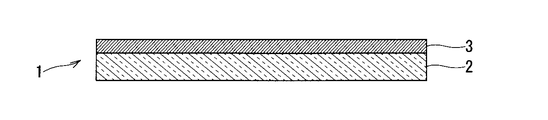
- FIG. 2 and FIG. 3 are cross-sectional views showing an example of the ceramic heat sink for pressure contact structure of the present invention.
- 1 is a ceramic heat sink for pressure contact structure
- 2 is a ceramic substrate
- 3 is a resin layer.
- the resin layer 3 there is a type provided on only one side of the ceramic substrate 2 as shown in FIG. 1, and a type provided on both sides of the ceramic substrate 2 as shown in FIG.
- the resin layer 3 may be provided on a surface where it is desired to ensure adhesion with the pressing member.
- the resin layer 3 may be provided on the entire ceramic substrate 2 so as to wrap the side surface of the ceramic substrate 2.
- the resin layer 3 may be provided on the portion of the ceramic heat sink 1 for the pressure contact structure that has the pressure contact structure, that is, the portion that receives the pressing force from the pressing members 4 and 4.
- an insertion hole such as a screw may be provided in the ceramic substrate 2.
- the ceramic substrate 2 is not particularly limited, such as an aluminum oxide (Al 2 O 3 ) substrate, an aluminum nitride (AlN) substrate, or a silicon nitride (Si 3 N 4 ) substrate.
- a ceramic substrate having a strength of 300 MPa or more is preferable.
- heat conductivity is 60 W / m * K or more.
- the ceramic substrate having a three-point bending strength of 300 MPa or more and a thermal conductivity of 60 W / m ⁇ K or more include an aluminum nitride substrate and a silicon nitride substrate.
- a ceramic substrate having high strength is preferable, and specifically, a silicon nitride substrate having a three-point bending strength of 600 MPa or more can be given.
- a resin layer having a durometer (shore) hardness (A type) of 70 or less is provided on the ceramic substrate.
- the durometer (shore) hardness (type A) is measured by a method according to JIS-K-6253, and the shore hardness is measured with a pressing time of 1 second.
- a durometer (shore) hardness (A type) of 70 or less is expressed as “A70 or less”.
- the Shore hardness of the resin layer is A70 or less, the lower limit is not particularly limited, but A10 or more is preferable. More preferably A30 ⁇ A60. If the Shore hardness is less than A10, the resin layer is too soft. If the pressing force when the pressure contact structure is taken is strong, the resin layer may be broken.
- the resin constituting the resin layer is not particularly limited as long as it has a Shore hardness of A70 or less when solidified, and is not particularly limited, such as a thermosetting resin that exhibits fluidity at 60 ° C. A resin is preferred.
- the thermosetting resin exhibiting fluidity at 60 ° C. is a material that liquefies and exhibits fluidity when the paste-like resin reaches 60 ° C. or higher.
- thermosetting resin that exhibits fluidity at 60 ° C.
- heat of 60 ° C. or higher is applied to form a pressure-contact structure, and the paste-like resin is once melted to impart fluidity, thereby providing the fineness of the ceramic substrate surface. Since the resin enters the visual unevenness, the average value of the voids existing at the interface between the ceramic substrate and the resin layer can be further reduced to 1 ⁇ m or less (including 0).
- the composition of the resin is not particularly limited, but examples of the resin exhibiting the above characteristics include a so-called phase change material.
- a second ceramic heat sink material for pressure contact structure is a ceramic heat sink material for pressure contact structure in which a resin layer is provided on a ceramic substrate, wherein the resin layer is a thermosetting resin exhibiting fluidity at 60 ° C. It is characterized by being formed by solidification.
- this second ceramic heat sink material for pressure contact structure applies a method of forming a pressure contact structure with a pressing member and solidifying the resin layer by applying heat when manufacturing a semiconductor module having a pressure contact structure. Can also be manufactured.
- the configurations of the first ceramic heat sink material for pressure contact structure and the second ceramic heat sink material for pressure contact structure preferably satisfy both, but are independently established.
- the average value of the voids existing at the interface between the ceramic substrate and the resin layer is determined by observing the interface between the ceramic substrate and the resin layer over a length of 200 ⁇ m in an arbitrary cross section, and the maximum diameter of the voids reflected there Ask for.
- the average value of the maximum diameters of individual voids is defined as “average value of voids”.
- the resin layer preferably contains inorganic filler particles. Since the resin has high insulating properties but low thermal conductivity, a resin whose thermal conductivity is improved by adding inorganic filler particles such as metal powder and ceramic powder to the resin may be used.
- the metal powder include Cu powder and Al powder
- examples of the ceramic powder include AlN powder, Si 3 N 4 powder, and MgO powder.
- AlN (aluminum nitride) powder is preferable because both insulation and thermal conductivity are good.
- the particle size of the inorganic filler particles is preferably 1/2 or less, more preferably 1/5 or less of the thickness of the resin layer. If the particle size is large, the filler particles may pop out from the resin layer when the pressure contact structure is taken, and the adhesion may be hindered.
- the content of the inorganic filler particles is preferably in the range of 20 to 60% by volume. If the amount is less than 20% by volume, the effect of addition is small. If the amount exceeds 60% by volume, the inorganic filler particles may jump out of the surface of the resin layer during press-contacting and hinder adhesion.
- the inorganic filler particles are preferably powder particles. Examples of the inorganic filler include a pointed filler such as a fiber or whisker.
- the inorganic filler particles are preferably powdery.
- the thickness of the resin layer is preferably 50 ⁇ m or less. Even if the thickness of the resin layer exceeds 50 ⁇ m, the void existing at the interface between the resin layer and the ceramic substrate can be reduced. However, if the resin layer is too thick, the heat dissipation is reduced, so that it is 50 ⁇ m or less, and further 30 ⁇ m or less. preferable.
- the lower limit value of the thickness of the resin layer is not particularly limited, but is preferably 5 ⁇ m or more. It is difficult to apply the resin paste thinly and uniformly to less than 5 ⁇ m, and from the viewpoint of manufacturability, it is preferably 5 ⁇ m or more, more preferably 10 ⁇ m or more. Note that the thickness of the resin layer may be controlled with respect to the surface having the pressure contact structure.
- the surface roughness Ra of the ceramic substrate is preferably 0.1 to 5 ⁇ m.
- the surface roughness Ra is preferably 5 ⁇ m or less.
- the surface roughness Ra is less than 0.1 ⁇ m, the surface of the ceramic substrate is too flat, and the anchor effect may not be sufficiently obtained, which may reduce the adhesion of the resin layer.
- the ceramic heat sink for pressure contact structure of the present invention is suitable for a semiconductor module, and particularly suitable for a semiconductor module in which a ceramic heat sink material for pressure contact structure is pressure contacted using a pressing member.
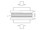
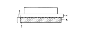
- 4 and 5 show an example of the pressure contact structure.
- 1 is a ceramic heat sink for pressure contact structure
- 4 is a pressing member
- 5 is a portion where the ceramic substrate 2 and the pressing member 4 are in direct contact.
- FIG. 4 shows an example of the pressure contact structure, which is fixed by pressing force from the upper and lower surfaces of the ceramic heat sink 1 for pressure contact via the pressing members 4 and 4.
- the ceramic heat sink 1 for pressure contact structure of the present invention has a Shore hardness. Since the soft resin layer of A70 or less is provided, the portion 5 where the pressing member 4 and the surface of the ceramic substrate 2 are in direct contact can be formed as shown in FIG.
- the portion 5 in which the pressing member 4 and the ceramic substrate 2 are in direct contact heat can be transferred between the pressing member 4 and the ceramic substrate 2 without the resin layer 3 being a thermal resistor. heat radiation since it can be improved. That is, the high thermal conductivity of the ceramic substrate 2 can be utilized.
- the portion 5 where the pressing member 4 and the ceramic substrate 2 are in direct contact is a point contact having a maximum diameter of 1 mm or less.
- the portion in direct contact is too large, the occurrence of cracks due to microscopic unevenness present on the surface of the ceramic substrate cannot be suppressed by the pressure contact structure as in the prior art. That is, the effect of providing the resin layer cannot be obtained. Therefore, point contact with a maximum diameter of 1 mm or less, and further 0.5 mm or less and 0.01 mm or less are preferable.
- the lower limit value of the point contact is not particularly limited, but is preferably 0.001 mm or more (1 ⁇ m or more). Moreover, it is preferable that a plurality of point contacts exist. When there are a plurality of small contact points, a synergistic effect can be obtained because an effect of providing a resin layer can be obtained while taking advantage of good heat dissipation of the ceramic substrate.
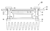
- FIG. 6 and FIG. 7 show an example of a semiconductor package having a pressure contact structure.
- reference numerals 1D, 1B and 1E are ceramic heat sinks for pressure contact structure
- 2 and 2D are ceramic substrates
- 7 are semiconductor elements
- 8 and 8A are pressing members
- 9 and 10 are insulating spacers
- 11 are heat dissipation members
- 12 and Reference numeral 13 denotes an insertion hole
- 14 denotes a fastening member (screw)
- 15 denotes a washer
- 16 denotes a hole (screwing hole).
- 6 shows a structural example in which the resin layer 3 is provided on one surface of the ceramic substrate 2D
- FIG. 7 shows a configuration example in which the resin layers 3 and 3 are provided on both surfaces of the ceramic substrate 2.
- the semiconductor module 20 includes a press-contact structure ceramic heat sink 1D provided with insertion holes 12 and 12, and a plate-shaped presser disposed facing the resin layer 3 of the press-contact structure ceramic heat sink 1D.
- a heat dissipating member (heat dissipating fin) 11 that dissipates heat generated in the element 7 and a fastening member (screw) 14 that tightens between the heat sink 1D for pressure contact structure and the heat dissipating member 11 are provided.
- a plate-like insulating spacer 9 is interposed between one surface of the semiconductor element 7 and the pressing member 8.
- a plate-like insulating spacer 10 is interposed between the other surface of the semiconductor element 7 and the heat dissipation member 11. Further, the semiconductor element 7 is sandwiched between the insulating spacer 9 and the insulating spacer 10. Further, the insulating spacer 9, the semiconductor element 7, and the insulating spacer 10 are sandwiched between the pressing member 8 disposed facing the insulating spacer 9 and the heat radiating member 11 disposed facing the insulating spacer 10. Is done.
- the ceramic heat sink 1D for pressure contact structure and the heat radiating member 11 are fastened using a fastening member 14.
- the fastening member 14 in this case is a screw, but is not limited to screwing as long as it can be fixed.
- the press-contact structure ceramic heat sink 1 ⁇ / b> D and the heat dissipating member 11 are tightened using the tightening member 14, so The member 8, the insulating spacer 9, the semiconductor element 7, and the insulating spacer 10 are pressed into contact with each other.
- the insertion holes 12 and 12 may be provided in the ceramic substrate 2D.
- the pressing member 8 is a plate-like member that comes into contact with the resin layer 3 of the ceramic heat sink 1D for pressure contact structure.
- a metal plate such as a copper plate is used.
- the pressing member 8 is interposed between the ceramic heat sink 1D for pressure contact structure and other members such as the insulating spacer 9.
- the pressing member 8 is brought into pressure contact with the semiconductor element 7 via the insulating spacer 9 by fastening the ceramic heat sink 1D for pressure contact structure and the heat radiating member 11 using the fastening member 14.
- the semiconductor element 7 is a single semiconductor element or an assembly including a plurality of semiconductor elements.
- Insulating spacers 9 and insulating spacers 10 are arranged in the vertical direction of the semiconductor element 7.
- a plate-like insulator such as a ceramic substrate is used.
- the heat radiating member 11 is a member that radiates heat generated in the semiconductor element 7.
- a hole 16 is provided above the heat dissipating member 11 in the drawing so that the tip of a screw 14 as a fastening member can be fitted together.
- a heat radiating fin is used as the heat radiating member 11, for example.
- the fastening member 14 fastens the pressure contact structure ceramic heat sink 1D and the heat radiating member 11.
- a screw is used as the fastening member 14.
- the body of the screw 14 as a fastening member is inserted into the insertion hole 12 of the ceramic heat sink 1D for pressure contact structure, and the tip of the screw 14 is inserted into the hole 16 of the heat dissipation member 11.
- the ceramic heat sink 1D for pressure contact structure and the heat radiating member 11 are tightened.
- a washer 15 is interposed between the head of the screw 14 and the ceramic heat sink 1D for pressure contact structure.
- the ceramic substrate 2D provided with the soft resin layer 3 having a Shore hardness of A70 or less and the surface of the pressing member 8 are strongly pressed.
- the resin layer 3 having flexibility of the ceramic heat sink 1D for pressure contact structure wraps microscopic irregularities present on the surface of the ceramic substrate 2D, the resin layer 3 of the ceramic heat sink 1D for pressure contact structure and the pressing member 8 is used. allowing intimate contact via.
- the resin layer 3 having flexibility can be deformed to directly contact the ceramic substrate and the pressing member.
- the pressing force at the time of pressure contact is 5 MPa or more
- the resin layer 3 having flexibility can be deformed to directly contact the ceramic substrate and the pressing member.
- the pressing force is excessively high, the ceramic substrate may be broken, so a pressing force of 5% or less of the three-point bending strength of the ceramic substrate 2D is used as a guide.
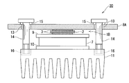
- FIG. 1 An example of a semiconductor module using the ceramic heat sink 1B for pressure contact structure in which the resin layers 3 and 3 are provided on both surfaces of the ceramic substrate 2 is shown in FIG.
- the semiconductor module 30 faces the ceramic heat sink 1B for pressure contact structure in which the resin layers 3 and 3 are provided on both front and back surfaces, and the resin layer 3 on one surface of the ceramic heat sink 1B for pressure contact structure.
- the plate-shaped pressing member 8A disposed, the semiconductor element 7 disposed facing the resin layer 3 on the other surface of the ceramic heat sink 1B for pressure contact structure, and the ceramic heat sink 1B for pressure contact structure among the surfaces of the semiconductor element 7
- a heat radiating member 11 for radiating heat generated in the semiconductor element 7 and a fastening member 14 for tightening between the pressing member 8A and the heat radiating member 11.
- a plate-like insulating spacer 9 is interposed between one surface of the semiconductor element 7 and the pressing member 8A.
- a plate-like insulating spacer 10 is interposed between the other surface of the semiconductor element 7 and the heat dissipation member 11.
- the semiconductor element 7 is sandwiched between the insulating spacer 9 and the insulating spacer 10. Further, the insulating spacer 9, the semiconductor element 7, and the insulating spacer 10 include a pressure contact structure ceramic heat sink 1 ⁇ / b> B disposed facing the insulating spacer 9 and a heat dissipation member 11 disposed facing the insulating spacer 10. It is sandwiched between. The pressing member 8 ⁇ / b> A and the heat radiating member 11 are fastened using the fastening member 14.
- the pressing member 8 ⁇ / b> A and the heat radiating member 11 are tightened using the tightening member 14, so that the pressure contact structure ceramic heat sink 1 ⁇ / b> B disposed between the pressing member 8 ⁇ / b> A and the heat radiating member 11.
- the insulating spacer 9, the semiconductor element 7, and the insulating spacer 10 are pressed against each other.
- the semiconductor module 30 shown in FIG. 7 uses a pressing member 8A provided with an insertion hole 12 instead of the ceramic heat sink 1D for pressure contact structure, as compared with the semiconductor module 20 shown in FIG.
- the difference is that a ceramic heat sink 1B for pressure contact structure in which the resin layers 3 are provided on both the front and back sides is used instead of 8, and the other points are the same. Therefore, the same reference numerals are given to the same components between the semiconductor module 30 shown in FIG. 7 and the semiconductor module 20 shown in FIG. 6, and the description of the configuration and operation thereof is omitted or simplified. To do.
- the shape and size of the insertion hole 13 are not particularly limited as long as the fastening member 14 such as a screw can be inserted or screwed. Further, the insertion hole 13 is not particularly limited with respect to the position and number of the pressing member 8A.
- the pressing member 8A presses other members such as the insulating spacer 9 through the press-contact structure ceramic heat sink 1B when the pressing member 8A and the heat radiating member 11 are tightened using the tightening member 14.
- the fastening member 14 is a member that fastens the pressing member 8 ⁇ / b> A and the heat radiating member 11.
- a screw is used as the fastening member 14.
- the body of the screw 14 as a fastening member is inserted into the washer 15 and the insertion hole 13 of the pressing member 8 ⁇ / b> A, and the tip of the screw 14 is the hole 16 of the heat dissipation member 11.
- the ceramic heat sink 1B for pressure contact structure and the heat radiating member 11 are tightened.
- a washer 15 is interposed between the head of the screw 14 and the pressing member 8A.
- the pressure contact structure ceramic heat sink 1 ⁇ / b> B, the insulating spacer 9, the semiconductor element 7, and the insulating spacer 10 disposed between the pressing member 8 ⁇ / b> A and the heat dissipation member 11 are pressed.
- the resin layer 3 on one surface of the ceramic heat sink 1B for pressure contact structure and the surface of the pressing member 8A, the resin layer 3 on the other surface of the ceramic heat sink 1B for pressure contact structure, and the surface of the insulating spacer 9 between is strongly pressed.
- the resin layer 3 having the flexibility of the ceramic heat sink 1B for pressure contact structure wraps the microscopic unevenness present on the surface of the ceramic substrate, close contact can be achieved.
- the ceramic substrate and the pressing member can be brought into direct contact by deforming the flexible resin layer.
- the pressing force is excessively high, the ceramic substrate may be broken, so a pressing force of 5% or less of the three-point bending strength of the ceramic substrate is used as a guide.
- the semiconductor module of this invention is not limited to screwing.
- a clamp that sandwiches the heat dissipation member 11 and the pressure contact structure ceramic heat sink or the heat dissipation member 11 and the pressing member can be used as the fastening member.
- a clamp it is not necessary to provide an insertion hole in the ceramic heat sink for pressure contact or the pressing member.
- a member capable of radiating heat generated from the semiconductor module may be used as a heat radiating member other than the heat radiating fins.
- a heat radiating sheet or the like can be used as the heat radiating member.
- a heat dissipation sheet for example, by using a clamp as a fastening member, the heat dissipation sheet and the ceramic heat sink for pressure contact structure are sandwiched, or the heat dissipation sheet and the pressing member are sandwiched. It is possible to form a semiconductor module having a pressure contact structure, and it is not necessary to provide an insertion hole in the ceramic heat sink or pressure member for pressure contact structure.
- the semiconductor modules 20 and 30 shown in FIGS. 6 and 7 are examples of the semiconductor module of the present invention.
- the semiconductor module of the present invention includes all of the structures that use a semiconductor element and that can press-contact a ceramic substrate provided with a resin layer and a pressing member.
- the manufacturing method of the ceramic heat sink for pressure contact structure of the present invention will be described.
- the manufacturing method of the ceramic heat sink for pressure contact structure of the present invention is not particularly limited, the following method may be mentioned as a method for obtaining it efficiently.
- a ceramic substrate preferably has a three-point bending strength of 500 MPa or more and a thermal conductivity of 60 W / m ⁇ K or more.
- the thickness of the ceramic substrate is preferably 0.2 to 1.0 mm. If the thickness is less than 0.2 mm, the ceramic substrate may be cracked when the pressure contact structure is formed. On the other hand, if the thickness exceeds 1.0 mm, the ceramic substrate itself becomes a thermal resistor, which may hinder heat dissipation.
- the surface roughness of the ceramic substrate is preferably 0.1 to 5 ⁇ m on the basis of Ra. Therefore, polishing processing such as honing processing is performed as necessary. In other words, if the surface roughness Ra is in the range of 0.1 to 5 ⁇ m on the baked surface, no particular polishing process is required.
- the inorganic filler particles are added to the resin paste.
- the average particle diameter of the inorganic filler particles is preferably 1/2 or less, more preferably 1/5 or less of the thickness of the resin layer to be formed.
- a resin layer is formed by applying a resin paste on a ceramic substrate and solidifying it.
- the resin is a thermosetting resin
- heat is applied to solidify, while when the resin is an ultraviolet curing type, the resin is cured by irradiation with ultraviolet rays.
- the resin which comprises a resin layer is a thermosetting resin which shows fluidity
- a resin having a Shore hardness of A70 or less after solidification is used. If the Shore hardness is A70 or less, a resin film may be used as the resin layer, or the resin film may be provided on the surface by thermocompression bonding.
- a pressure contact structure ceramic heat sink is sandwiched and pressed by a pressing member.
- thermosetting resin exhibiting fluidity at 60 ° C. or higher when used as the resin layer, a thermosetting resin layer exhibiting fluidity at 60 ° C. or higher is formed on the ceramic substrate, and then heat treated to solidify. To form a pressure contact structure.
- the resin layer can be filled in the gap between the pressing member and the ceramic substrate, so that the void existing at the interface between the ceramic substrate and the resin layer. the can also be zero. Furthermore, if this operation is performed in a vacuum in the mounting process of the semiconductor module, the gap between the resin layer and the contact member can be made zero.
- Example 1 (Examples 1 to 9 and Comparative Example 1)
- a silicon nitride substrate (thermal conductivity 90 W / m ⁇ K, three-point bending strength 600 MPa) having a length of 50 mm ⁇ width of 50 mm ⁇ thickness of 0.32 mm was prepared.
- the surface roughness Ra was changed by surface processing such as honing processing or polishing using a diamond grindstone.
- a silicone resin layer having a Shore hardness after curing of A70 or less on both surfaces of such a silicon nitride substrate, a ceramic heat sink for press contact structure according to each example was prepared.
- Example 2 For comparison, a ceramic heat sink for pressure contact structure having the same structure as Example 1 was prepared except that a resin layer having a Shore hardness of A100 was provided.
- the average value of gaps (voids) existing at the interface between the ceramic substrate and the resin layer was determined.
- an arbitrary interface between the ceramic substrate and the resin layer was observed over a length of 200 ⁇ m, and the maximum diameter of the voids reflected there was determined.
- the average value of the maximum diameters of the individual voids was defined as “average value of voids”.
- a silicon nitride substrate (thermal conductivity 80 W / m ⁇ K, three-point bending strength 700 MPa) having a length of 50 mm ⁇ width of 50 mm ⁇ thickness of 0.32 mm was prepared.
- the surface roughness Ra was changed by surface processing such as honing processing or polishing using a diamond grindstone.
- a thermosetting resin paste exhibiting fluidity at 60 ° C. was applied to both sides of such a silicon nitride substrate. The applied resin layer was naturally dried to obtain a resin paste layer.
- a copper plate corresponding to a pressing member is pressed at a pressure of 2 MPa, heated to a temperature of 60 to 120 ° C.
- the resin if the resin has fluidity in the pressure contact structure and then solidified, the resin will enter microscopic irregularities on the substrate surface.
- the average value of the gap at the interface between the ceramic substrate and the resin layer could be very small, 1 ⁇ m or less (including zero).
- Example 13 to 16 While using an aluminum oxide substrate (thermal conductivity 20 W / m ⁇ K, three-point bending strength 400 MPa) having a length of 50 mm ⁇ width of 50 mm ⁇ thickness of 0.635 mm, Examples 13 to 14 were used, whereas length 50 mm ⁇ width 50 mm X Resin having a Shore hardness of A70 or less on both surfaces of each substrate as Examples 15 to 16 using a 0.635 mm thick aluminum nitride substrate (thermal conductivity 170 W / m ⁇ K, three-point bending strength 500 MPa) A layer was provided. Similar to Example 1, the average value of the gaps existing at the interface between the ceramic substrate and the resin layer was determined. The results are shown in Table 3 below.
- the average value of the voids at the interface between the ceramic substrate and the resin layer can be reduced to 3 ⁇ m or less by forming a resin layer having a Shore hardness after solidification of A70 or less. did it.
- Example 17 A ceramic heat sink material for pressure contact structure similar to that of Example 2 was prepared except that the thickness of the ceramic substrate was changed to 0.20 mm and 1.0 mm. Specifically, as Example 17, a silicon nitride substrate (thermal conductivity 90 W / m ⁇ K, three-point bending strength 600 MPa) having a length of 50 mm ⁇ width of 50 mm ⁇ thickness of 0.20 mm was prepared. Measurements similar to those in Example 2 were performed. The measurement results are shown in Table 4 below.
- the thermal resistance was measured by sandwiching the oxygen heat sink for pressure contact structure of each example and comparative example from both sides with an oxygen-free copper block having a diameter of 40 mm ⁇ height of 16 mm, a heater on the upper copper block, Water-cooled cooling fins were brought into contact with the copper block. In this state, a load of 5 MPa was applied, the heater was heated and maintained at 70 ° C., and cooling water was passed through the cooling fins and maintained at 30 ° C. Temperature measuring holes for temperature measurement were provided above and below each copper block, and the heat flux was calculated.
- Comparative Example 2 uses the same silicon nitride substrate as in Example 1 except that no resin layer is provided
- Comparative Example 3 uses the same aluminum oxide substrate as Example 13 except that no resin layer is provided.
- the same measurement as in the example was performed using the same aluminum nitride substrate as in Example 15 except that the resin layer was not provided as Comparative Example 4. The results are shown in Table 5.
- Examples 1B-18B semiconductor modules were manufactured using the pressure contact structures of Examples 1 to 18.
- the semiconductor module has the structure shown in FIG.
- the pressure by screwing was 3 MPa.
- Durability was measured for each semiconductor module. Durability was confirmed by the presence or absence of cracks in the silicon nitride substrate when the semiconductor module structure was subjected to vibration that reciprocated 500 times in 50 minutes in one minute for 100 hours continuously.
- the maximum diameter of the portion where the pressing member and the ceramic substrate are in direct contact was obtained.
- the maximum diameter was measured by observing a cross section with a screw pressing pressure of 3 MPa, and calculating the average value of the voids. The results are shown in Table 6.
- the semiconductor module according to each example was excellent in durability. Further, the maximum diameter (mm) of the portion where the pressing member and the ceramic substrate are in direct contact was as small as 1 mm or less. A plurality of portions where the pressing member and the ceramic substrate were in direct contact were confirmed in any of the examples.
Landscapes
- Engineering & Computer Science (AREA)
- Physics & Mathematics (AREA)
- Thermal Sciences (AREA)
- Ceramic Engineering (AREA)
- Mechanical Engineering (AREA)
- General Engineering & Computer Science (AREA)
- Microelectronics & Electronic Packaging (AREA)
- Cooling Or The Like Of Semiconductors Or Solid State Devices (AREA)
- Chemical & Material Sciences (AREA)
Abstract
Description
(実施例1~9および比較例1)
セラミックス基板として、縦50mm×横50mm×厚さ0.32mmの窒化珪素基板(熱伝導率90W/m・K、3点曲げ強度600MPa)を用意した。次にホーニング加工やダイヤモンド砥石を使った研磨などの表面加工により表面粗さRaを変えた。このような窒化珪素基板の両面に硬化後のショア硬度がA70以下となるシリコーン樹脂層を形成することにより、各実施例に係る圧接構造用セラミックスヒートシンクを用意した。

セラミックス基板として、縦50mm×横50mm×厚さ0.32mmの窒化珪素基板(熱伝導率80W/m・K、3点曲げ強度700MPa)を用意した。次にホーニング加工やダイヤモンド砥石を使った研磨などの表面加工により表面粗さRaを変えた。このような窒化珪素基板の両面に60℃で流動性を示す熱硬化性樹脂ペーストを塗布した。塗布した樹脂層を自然乾燥させて樹脂ペースト層とした。樹脂層上に押さえ部材相当として銅板を押圧力2MPaで押さえた状態で温度60~120℃×15~30分に加熱して樹脂ペースト層を溶かして、その後、自然乾燥により固化させ樹脂層とした。各実施例について実施例1と同様にセラミックス基板と樹脂層との界面にある隙間の平均値を求めた。その結果を下記表2に示す。
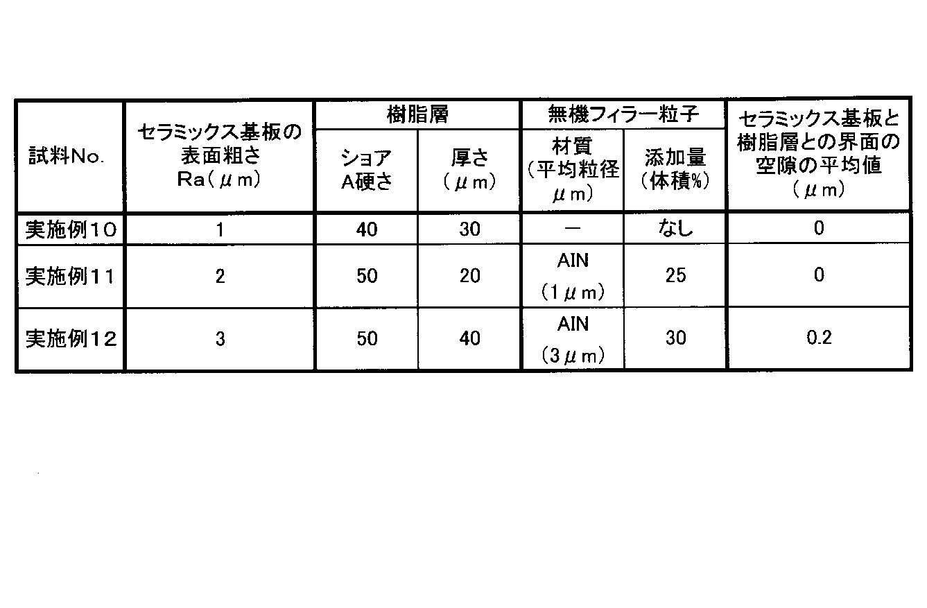
縦50mm×横50mm×厚さ0.635mmの酸化アルミニウム基板(熱伝導率20W/m・K、3点曲げ強度400MPa)を用いたものを実施例13~14とする一方、縦50mm×横50mm×厚さ0.635mmの窒化アルミニウム基板(熱伝導率170W/m・K、3点曲げ強度500MPa)を用いたものを実施例15~16として、各基板の両面にショア硬度がA70以下の樹脂層を設けた。実施例1と同様にセラミックス基板と樹脂層との界面に存在する隙間の平均値を求めた。その結果を下記表3に示す。

セラミックス基板の厚さを0.20mm、1.0mmに変えた以外は実施例2と同様の圧接構造用セラミックスヒートシンク材を用意した。具体的には、実施例17として、縦50mm×横50mm×厚さ0.20mmの窒化珪素基板(熱伝導率90W/m・K、3点曲げ強度600MPa)を用意した。実施例2と同様の測定を行った。下記表4にその測定結果を示す。

次に実施例1~18および比較例1の圧接構造用セラミックスヒートシンクを用いて熱抵抗の測定を行った。

次に、実施例1~18の圧接構造を用いて半導体モジュールを作製した。半導体モジュールは図7の構造のものとした。ねじ止めによる圧力は3MPaとした。各半導体モジュールについて耐久性を測定した。耐久性は半導体モジュール構造体を、50cm間を一分間で500回往復する振動を100時間連続で付加したときの窒化珪素基板のクラックの発生の有無で確認した。

2、2D…セラミックス基板
3…樹脂層
4…押え部材
5…セラミックス基板表面と押さえ部材が直接接触した部分
7…半導体素子
8、8A…押え部材
9、10…絶縁性スペーサ
11…放熱部材(放熱フィン)
12…セラミックス基板の挿通孔
13…押え部材の挿通孔
14…ねじ(締め付け部材)
15…ワッシャ
16…孔部
20、30…半導体モジュール
Claims (15)
- セラミックス基板上に樹脂層を設けた圧接構造用セラミックスヒートシンク材において、上記樹脂層のデュロメーター(ショア)硬さ(A型)が70以下であり、セラミックス基板と樹脂層との界面に存在する空隙の平均値が3μm以下であることを特徴とする圧接構造用セラミックスヒートシンク材。
- 前記樹脂層は60℃で流動性を示す熱硬化型樹脂が固化して形成されていることを特徴とする請求項1記載の圧接構造用セラミックスヒートシンク材。
- セラミックス基板上に樹脂層を設けた圧接構造用セラミックスヒートシンク材において、上記樹脂層は60℃で流動性を示す熱硬化型樹脂を固化して形成されたものであることを特徴とする圧接構造用セラミックスヒートシンク材。
- 前記樹脂層は無機フィラー粒子を含有していることを特徴とする請求項1または請求項3記載の圧接構造用セラミックスヒートシンク材。
- 前記樹脂層のデュロメーター(ショア)硬さ(A型)が10以上であることを特徴とする請求項1ないし請求項4のいずれか1項に記載の圧接構造用セラミックスヒートシンク材。
- 前記セラミックス基板が、窒化珪素基板、酸化アルミニウム基板、窒化アルミニウム基板のいずれか1種であることを特徴とする請求項1ないし請求項5のいずれか1項に記載の圧接構造用セラミックスヒートシンク材。
- 前記樹脂層の厚さが50μm以下であることを特徴とする請求項1ないし請求項6のいずれか1項に記載の圧接構造用セラミックスヒートシンク材。
- 前記セラミックス基板の表面粗さRaが0.1~5μmであることを特徴とする請求項1ないし請求項7のいずれか1項に記載の圧接構造用セラミックスヒートシンク材。
- 請求項1ないし請求項8のいずれか1項に記載の圧接構造用セラミックスヒートシンク材を押さえ部材によって圧接したことを特徴とする半導体モジュール。
- 前記押さえ部材により圧接構造をとったときに、押さえ部材とセラミックス基板との表面が直接接触している部分があることを特徴とする請求項9記載の半導体モジュール。
- 直接接触している部分が、最大径1mm以下の点接触であることを特徴とする請求項10記載の半導体モジュール。
- 点接触が複数箇所存在することを特徴とする請求項11記載の半導体モジュール。
- 圧接構造用セラミックスヒートシンク材を押さえ部材により圧接する構造を有する半導体モジュールの製造方法において、
樹脂層のデュロメーター(ショア)硬さ(A型)が70以下であり、セラミックス基板と樹脂層との界面に存在する空隙の平均値が3μm以下であるセラミックス基板上に樹脂層を設けた圧接構造用セラミックスヒートシンク材を用意し、
この圧接構造用セラミックスヒートシンク材を押さえ部材で圧接するときに、上記押さえ部材とセラミックス基板との表面が直接接触している部分が形成される圧力で圧接することを特徴とする半導体モジュールの製造方法。 - 圧接構造用セラミックスヒートシンク材を押さえ部材により圧接する構造を有する半導体モジュールの製造方法において、
セラミックス基板上に60℃で流動性を示す熱硬化樹脂層を形成して圧接構造用セラミックスヒートシンク材を作製する工程と、
押さえ部材によって圧接構造用セラミックスヒートシンク材を圧接する圧接工程と、
60℃以上の熱を付加して60℃で流動性を示す熱硬化樹脂層を固化させる固化工程と、
を具備することを特徴とする半導体モジュールの製造方法。 - 押さえ部材とセラミックス基板との表面が直接接触している部分が形成されていることを特徴とする請求項14記載の半導体モジュールの製造方法。
Priority Applications (4)
| Application Number | Priority Date | Filing Date | Title |
|---|---|---|---|
| JP2012545706A JP5996435B2 (ja) | 2010-11-22 | 2011-11-17 | 半導体モジュールおよび半導体モジュールの製造方法 |
| US13/988,555 US9057569B2 (en) | 2010-11-22 | 2011-11-17 | Ceramic heat sink material for pressure contact structure and semiconductor module using the same |
| CN201180055906.8A CN103222047B (zh) | 2010-11-22 | 2011-11-17 | 用于压力接触结构的陶瓷热沉材料、使用其的半导体模块和用于制造半导体模块的方法 |
| KR1020137012945A KR101472234B1 (ko) | 2010-11-22 | 2011-11-17 | 압접 구조용 세라믹 히트 싱크재, 그를 이용한 반도체 모듈 및 반도체 모듈의 제조 방법 |
Applications Claiming Priority (2)
| Application Number | Priority Date | Filing Date | Title |
|---|---|---|---|
| JP2010-260541 | 2010-11-22 | ||
| JP2010260541 | 2010-11-22 |
Publications (1)
| Publication Number | Publication Date |
|---|---|
| WO2012070463A1 true WO2012070463A1 (ja) | 2012-05-31 |
Family
ID=46145807
Family Applications (1)
| Application Number | Title | Priority Date | Filing Date |
|---|---|---|---|
| PCT/JP2011/076512 Ceased WO2012070463A1 (ja) | 2010-11-22 | 2011-11-17 | 圧接構造用セラミックスヒートシンク材およびそれを用いた半導体モジュール並びに半導体モジュールの製造方法 |
Country Status (5)
| Country | Link |
|---|---|
| US (1) | US9057569B2 (ja) |
| JP (2) | JP5996435B2 (ja) |
| KR (1) | KR101472234B1 (ja) |
| CN (1) | CN103222047B (ja) |
| WO (1) | WO2012070463A1 (ja) |
Cited By (7)
| Publication number | Priority date | Publication date | Assignee | Title |
|---|---|---|---|---|
| US20130241046A1 (en) * | 2010-11-22 | 2013-09-19 | Toshiba Materials Co., Ltd. | Ceramic heat sink material for pressure contact structure, semiconductor module using the same, and method for manufacturing semiconductor module |
| JP2014116375A (ja) * | 2012-12-07 | 2014-06-26 | Maruwa Co Ltd | 放熱構造体 |
| JP2014534645A (ja) * | 2012-10-24 | 2014-12-18 | 華為技術有限公司Huawei Technologies Co.,Ltd. | 熱パッド、熱パッドを製造する方法、放熱装置および電子装置 |
| US20150118505A1 (en) * | 2012-07-07 | 2015-04-30 | Dexerials Corporation | Method of producing heat conductive sheet |
| WO2019138762A1 (ja) * | 2018-01-12 | 2019-07-18 | Necプラットフォームズ株式会社 | 放熱構造体、および放熱方法 |
| US20220077656A1 (en) * | 2020-09-08 | 2022-03-10 | Hewlett Packard Enterprise Development Lp | Thermal management for hybrid lasers |
| CN117645493A (zh) * | 2023-11-30 | 2024-03-05 | 西南交通大学 | 一种振荡压力辅助陶瓷连接方法 |
Families Citing this family (7)
| Publication number | Priority date | Publication date | Assignee | Title |
|---|---|---|---|---|
| JP3368674B2 (ja) | 1993-08-11 | 2003-01-20 | 日産自動車株式会社 | 傘歯車の鍛造方法 |
| CN105684144B (zh) | 2013-09-10 | 2019-11-12 | 三菱电机株式会社 | 半导体装置、半导体模块 |
| US10629513B2 (en) * | 2015-06-04 | 2020-04-21 | Eaton Intelligent Power Limited | Ceramic plated materials for electrical isolation and thermal transfer |
| JP2017050493A (ja) * | 2015-09-04 | 2017-03-09 | 株式会社東芝 | 電子機器 |
| CN207869432U (zh) * | 2018-03-07 | 2018-09-14 | 东莞市国研电热材料有限公司 | 一种多温区陶瓷发热体 |
| JP7198178B2 (ja) | 2019-08-16 | 2022-12-28 | デンカ株式会社 | セラミックス基板、回路基板及びその製造方法、並びにパワーモジュール |
| CN112811922B (zh) * | 2021-01-20 | 2021-11-02 | 中国科学院上海硅酸盐研究所 | 一种覆铜板的氮化硅陶瓷基片及其制备方法 |
Citations (5)
| Publication number | Priority date | Publication date | Assignee | Title |
|---|---|---|---|---|
| JPS6079752U (ja) * | 1983-11-08 | 1985-06-03 | 株式会社東芝 | 電力用半導体スタツク |
| JPH01305548A (ja) * | 1988-05-26 | 1989-12-08 | Bergquist Co:The | 放熱取付け装置 |
| JP2003152148A (ja) * | 2001-03-19 | 2003-05-23 | Matsushita Electric Ind Co Ltd | 熱伝導性基板の製造方法 |
| JP2009081253A (ja) * | 2007-09-26 | 2009-04-16 | Nitto Shinko Kk | 絶縁シート |
| WO2011010597A1 (ja) * | 2009-07-24 | 2011-01-27 | 株式会社東芝 | 窒化珪素製絶縁シートおよびそれを用いた半導体モジュール構造体 |
Family Cites Families (23)
| Publication number | Priority date | Publication date | Assignee | Title |
|---|---|---|---|---|
| JPS5718386A (en) * | 1980-07-09 | 1982-01-30 | Mitsubishi Electric Corp | Method of flattening surface of board |
| JPS6079752A (ja) * | 1983-10-06 | 1985-05-07 | Toshiba Corp | 半導体素子搭載用基板 |
| JPH03234045A (ja) * | 1990-02-09 | 1991-10-18 | Toshiba Corp | 窒化アルミニウム基板およびこれを用いた半導体モジュール |
| JPH0794863A (ja) * | 1993-09-20 | 1995-04-07 | Fujitsu Ltd | セラミック基板の表面を平坦化する方法 |
| JP2001196512A (ja) * | 2000-01-11 | 2001-07-19 | Mitsubishi Electric Corp | 半導体装置 |
| JP3879361B2 (ja) * | 2000-03-21 | 2007-02-14 | 株式会社デンソー | 半導体装置の実装構造およびその実装方法 |
| JP5172738B2 (ja) | 2000-10-27 | 2013-03-27 | 株式会社東芝 | 半導体モジュールおよびそれを用いた電子機器 |
| JP4770059B2 (ja) * | 2001-05-24 | 2011-09-07 | パナソニック株式会社 | セラミック多層基板の製造方法 |
| JP2003192462A (ja) | 2001-12-25 | 2003-07-09 | Toshiba Corp | 窒化珪素回路基板およびその製造方法 |
| JP2003197836A (ja) * | 2001-12-27 | 2003-07-11 | Toshiba Corp | 圧接構造用スペーサおよびその製造方法 |
| JP2003321554A (ja) * | 2002-04-26 | 2003-11-14 | Polymatech Co Ltd | 熱伝導性成形体及びその製造方法 |
| JP2005116767A (ja) * | 2003-10-07 | 2005-04-28 | Ngk Spark Plug Co Ltd | 放熱部材並びに回路基板及び半導体部品 |
| JP4451746B2 (ja) * | 2004-08-31 | 2010-04-14 | 京セラ株式会社 | 電気素子冷却モジュール |
| JP5046086B2 (ja) * | 2006-09-14 | 2012-10-10 | 日立金属株式会社 | セラミックス基板、これを用いたセラミックス回路基板及び半導体モジュール |
| DE102008009510B3 (de) * | 2008-02-15 | 2009-07-16 | Danfoss Silicon Power Gmbh | Verfahren zum Niedertemperatur-Drucksintern |
| JP4798171B2 (ja) * | 2008-05-16 | 2011-10-19 | 三菱マテリアル株式会社 | パワーモジュール用基板、パワーモジュール及びパワーモジュール用基板の製造方法 |
| JP5366859B2 (ja) * | 2010-03-04 | 2013-12-11 | 株式会社東芝 | 窒化珪素基板およびそれを用いた半導体モジュール |
| US8927339B2 (en) * | 2010-11-22 | 2015-01-06 | Bridge Semiconductor Corporation | Method of making thermally enhanced semiconductor assembly with bump/base/flange heat spreader and build-up circuitry |
| KR101472234B1 (ko) * | 2010-11-22 | 2014-12-11 | 가부시끼가이샤 도시바 | 압접 구조용 세라믹 히트 싱크재, 그를 이용한 반도체 모듈 및 반도체 모듈의 제조 방법 |
| JP5502805B2 (ja) * | 2011-06-08 | 2014-05-28 | 日立オートモティブシステムズ株式会社 | パワーモジュールおよびそれを用いた電力変換装置 |
| US8569109B2 (en) * | 2011-06-30 | 2013-10-29 | Infineon Technologies Ag | Method for attaching a metal surface to a carrier, a method for attaching a chip to a chip carrier, a chip-packaging module and a packaging module |
| JP2013167583A (ja) * | 2012-02-16 | 2013-08-29 | Tatsuya Ishibashi | 衝突・反発式材料試験システム |
| JP6379497B2 (ja) * | 2014-01-28 | 2018-08-29 | 株式会社リコー | 定着部材、定着装置及び画像形成装置 |
-
2011
- 2011-11-17 KR KR1020137012945A patent/KR101472234B1/ko active Active
- 2011-11-17 CN CN201180055906.8A patent/CN103222047B/zh active Active
- 2011-11-17 JP JP2012545706A patent/JP5996435B2/ja active Active
- 2011-11-17 WO PCT/JP2011/076512 patent/WO2012070463A1/ja not_active Ceased
- 2011-11-17 US US13/988,555 patent/US9057569B2/en active Active
-
2016
- 2016-06-14 JP JP2016118119A patent/JP6224171B2/ja active Active
Patent Citations (5)
| Publication number | Priority date | Publication date | Assignee | Title |
|---|---|---|---|---|
| JPS6079752U (ja) * | 1983-11-08 | 1985-06-03 | 株式会社東芝 | 電力用半導体スタツク |
| JPH01305548A (ja) * | 1988-05-26 | 1989-12-08 | Bergquist Co:The | 放熱取付け装置 |
| JP2003152148A (ja) * | 2001-03-19 | 2003-05-23 | Matsushita Electric Ind Co Ltd | 熱伝導性基板の製造方法 |
| JP2009081253A (ja) * | 2007-09-26 | 2009-04-16 | Nitto Shinko Kk | 絶縁シート |
| WO2011010597A1 (ja) * | 2009-07-24 | 2011-01-27 | 株式会社東芝 | 窒化珪素製絶縁シートおよびそれを用いた半導体モジュール構造体 |
Cited By (13)
| Publication number | Priority date | Publication date | Assignee | Title |
|---|---|---|---|---|
| US20130241046A1 (en) * | 2010-11-22 | 2013-09-19 | Toshiba Materials Co., Ltd. | Ceramic heat sink material for pressure contact structure, semiconductor module using the same, and method for manufacturing semiconductor module |
| US9057569B2 (en) * | 2010-11-22 | 2015-06-16 | Kabushiki Kaisha Toshiba | Ceramic heat sink material for pressure contact structure and semiconductor module using the same |
| US20150118505A1 (en) * | 2012-07-07 | 2015-04-30 | Dexerials Corporation | Method of producing heat conductive sheet |
| US10336929B2 (en) * | 2012-07-07 | 2019-07-02 | Dexerials Corporation | Method of producing heat conductive sheet |
| JP2014534645A (ja) * | 2012-10-24 | 2014-12-18 | 華為技術有限公司Huawei Technologies Co.,Ltd. | 熱パッド、熱パッドを製造する方法、放熱装置および電子装置 |
| JP2014116375A (ja) * | 2012-12-07 | 2014-06-26 | Maruwa Co Ltd | 放熱構造体 |
| WO2019138762A1 (ja) * | 2018-01-12 | 2019-07-18 | Necプラットフォームズ株式会社 | 放熱構造体、および放熱方法 |
| JP2019125612A (ja) * | 2018-01-12 | 2019-07-25 | Necプラットフォームズ株式会社 | 放熱構造体、および放熱方法 |
| US11229114B2 (en) | 2018-01-12 | 2022-01-18 | Nec Platforms, Ltd. | Heat dissipation structure and heat dissipation method |
| US20220077656A1 (en) * | 2020-09-08 | 2022-03-10 | Hewlett Packard Enterprise Development Lp | Thermal management for hybrid lasers |
| US11876345B2 (en) * | 2020-09-08 | 2024-01-16 | Hewlett Packard Enterprise Development Lp | Thermal management for hybrid lasers |
| CN117645493A (zh) * | 2023-11-30 | 2024-03-05 | 西南交通大学 | 一种振荡压力辅助陶瓷连接方法 |
| CN117645493B (zh) * | 2023-11-30 | 2024-06-04 | 西南交通大学 | 一种振荡压力辅助陶瓷连接方法 |
Also Published As
| Publication number | Publication date |
|---|---|
| CN103222047B (zh) | 2016-01-06 |
| US20130241046A1 (en) | 2013-09-19 |
| KR101472234B1 (ko) | 2014-12-11 |
| CN103222047A (zh) | 2013-07-24 |
| JP2016181715A (ja) | 2016-10-13 |
| KR20130079601A (ko) | 2013-07-10 |
| US9057569B2 (en) | 2015-06-16 |
| JP5996435B2 (ja) | 2016-09-21 |
| JPWO2012070463A1 (ja) | 2014-05-19 |
| JP6224171B2 (ja) | 2017-11-01 |
Similar Documents
| Publication | Publication Date | Title |
|---|---|---|
| JP6224171B2 (ja) | 半導体モジュールの製造方法 | |
| JP5488619B2 (ja) | パワーモジュール用基板及びパワーモジュール | |
| CN107408538B (zh) | 电路基板及半导体装置 | |
| EP2833398B1 (en) | Power module substrate, and method for manufacturing a power module substrate | |
| CN104718616B (zh) | 自带散热器的功率模块用基板、自带散热器的功率模块及自带散热器的功率模块用基板的制造方法 | |
| JP5675610B2 (ja) | 窒化珪素製絶縁シートおよびそれを用いた半導体モジュール構造体 | |
| JP7151583B2 (ja) | ヒートシンク付き絶縁回路基板 | |
| EP3605601A1 (en) | Method for producing insulated circuit board with heat sink | |
| JP5699442B2 (ja) | パワーモジュール用基板及びパワーモジュール | |
| EP4120335A1 (en) | Heat sink integrated insulating circuit board | |
| KR102359146B1 (ko) | 저항기 및 저항기의 제조 방법 | |
| TW202243156A (zh) | 散熱片一體型絕緣電路基板 | |
| TWI294175B (ja) | ||
| JP2010192717A (ja) | 冷却構造 | |
| WO2019189090A1 (ja) | ヒートシンク付き絶縁回路基板の製造方法 | |
| JP2009266983A (ja) | 放熱構造及び該放熱構造の製造方法並びに該放熱構造を用いた放熱装置 | |
| JP2005285885A (ja) | 半導体装置 | |
| JP5659542B2 (ja) | 絶縁基板及びパワーモジュール | |
| TW202331949A (zh) | 金屬基材基板 | |
| JPH08222670A (ja) | 半導体素子搭載用パッケージ | |
| JP2019149514A (ja) | 放熱板付絶縁回路基板、及び、放熱板付絶縁回路基板の製造方法 | |
| JP2025159698A (ja) | 半導体装置 | |
| JP2026017137A (ja) | 電子装置および電子装置の製造方法 |
Legal Events
| Date | Code | Title | Description |
|---|---|---|---|
| 121 | Ep: the epo has been informed by wipo that ep was designated in this application |
Ref document number: 11842720 Country of ref document: EP Kind code of ref document: A1 |
|
| ENP | Entry into the national phase |
Ref document number: 2012545706 Country of ref document: JP Kind code of ref document: A |
|
| ENP | Entry into the national phase |
Ref document number: 20137012945 Country of ref document: KR Kind code of ref document: A |
|
| WWE | Wipo information: entry into national phase |
Ref document number: 13988555 Country of ref document: US |
|
| NENP | Non-entry into the national phase |
Ref country code: DE |
|
| 122 | Ep: pct application non-entry in european phase |
Ref document number: 11842720 Country of ref document: EP Kind code of ref document: A1 |