WO2012063585A1 - Source de lumière pompée à faisceau d'électrons - Google Patents
Source de lumière pompée à faisceau d'électrons Download PDFInfo
- Publication number
- WO2012063585A1 WO2012063585A1 PCT/JP2011/073292 JP2011073292W WO2012063585A1 WO 2012063585 A1 WO2012063585 A1 WO 2012063585A1 JP 2011073292 W JP2011073292 W JP 2011073292W WO 2012063585 A1 WO2012063585 A1 WO 2012063585A1
- Authority
- WO
- WIPO (PCT)
- Prior art keywords
- electron beam
- light emitting
- semiconductor light
- source
- emitting element
- Prior art date
Links
Images


Classifications
-
- H—ELECTRICITY
- H01—ELECTRIC ELEMENTS
- H01S—DEVICES USING THE PROCESS OF LIGHT AMPLIFICATION BY STIMULATED EMISSION OF RADIATION [LASER] TO AMPLIFY OR GENERATE LIGHT; DEVICES USING STIMULATED EMISSION OF ELECTROMAGNETIC RADIATION IN WAVE RANGES OTHER THAN OPTICAL
- H01S5/00—Semiconductor lasers
- H01S5/04—Processes or apparatus for excitation, e.g. pumping, e.g. by electron beams
- H01S5/041—Optical pumping
-
- B—PERFORMING OPERATIONS; TRANSPORTING
- B82—NANOTECHNOLOGY
- B82Y—SPECIFIC USES OR APPLICATIONS OF NANOSTRUCTURES; MEASUREMENT OR ANALYSIS OF NANOSTRUCTURES; MANUFACTURE OR TREATMENT OF NANOSTRUCTURES
- B82Y20/00—Nanooptics, e.g. quantum optics or photonic crystals
-
- H—ELECTRICITY
- H01—ELECTRIC ELEMENTS
- H01J—ELECTRIC DISCHARGE TUBES OR DISCHARGE LAMPS
- H01J63/00—Cathode-ray or electron-stream lamps
- H01J63/02—Details, e.g. electrode, gas filling, shape of vessel
-
- H—ELECTRICITY
- H01—ELECTRIC ELEMENTS
- H01J—ELECTRIC DISCHARGE TUBES OR DISCHARGE LAMPS
- H01J63/00—Cathode-ray or electron-stream lamps
- H01J63/06—Lamps with luminescent screen excited by the ray or stream
-
- H—ELECTRICITY
- H01—ELECTRIC ELEMENTS
- H01S—DEVICES USING THE PROCESS OF LIGHT AMPLIFICATION BY STIMULATED EMISSION OF RADIATION [LASER] TO AMPLIFY OR GENERATE LIGHT; DEVICES USING STIMULATED EMISSION OF ELECTROMAGNETIC RADIATION IN WAVE RANGES OTHER THAN OPTICAL
- H01S5/00—Semiconductor lasers
- H01S5/04—Processes or apparatus for excitation, e.g. pumping, e.g. by electron beams
-
- H—ELECTRICITY
- H01—ELECTRIC ELEMENTS
- H01L—SEMICONDUCTOR DEVICES NOT COVERED BY CLASS H10
- H01L2224/00—Indexing scheme for arrangements for connecting or disconnecting semiconductor or solid-state bodies and methods related thereto as covered by H01L24/00
- H01L2224/01—Means for bonding being attached to, or being formed on, the surface to be connected, e.g. chip-to-package, die-attach, "first-level" interconnects; Manufacturing methods related thereto
- H01L2224/42—Wire connectors; Manufacturing methods related thereto
- H01L2224/47—Structure, shape, material or disposition of the wire connectors after the connecting process
- H01L2224/48—Structure, shape, material or disposition of the wire connectors after the connecting process of an individual wire connector
- H01L2224/4805—Shape
- H01L2224/4809—Loop shape
- H01L2224/48091—Arched
-
- H—ELECTRICITY
- H01—ELECTRIC ELEMENTS
- H01S—DEVICES USING THE PROCESS OF LIGHT AMPLIFICATION BY STIMULATED EMISSION OF RADIATION [LASER] TO AMPLIFY OR GENERATE LIGHT; DEVICES USING STIMULATED EMISSION OF ELECTROMAGNETIC RADIATION IN WAVE RANGES OTHER THAN OPTICAL
- H01S5/00—Semiconductor lasers
- H01S5/02—Structural details or components not essential to laser action
- H01S5/022—Mountings; Housings
- H01S5/02208—Mountings; Housings characterised by the shape of the housings
-
- H—ELECTRICITY
- H01—ELECTRIC ELEMENTS
- H01S—DEVICES USING THE PROCESS OF LIGHT AMPLIFICATION BY STIMULATED EMISSION OF RADIATION [LASER] TO AMPLIFY OR GENERATE LIGHT; DEVICES USING STIMULATED EMISSION OF ELECTROMAGNETIC RADIATION IN WAVE RANGES OTHER THAN OPTICAL
- H01S5/00—Semiconductor lasers
- H01S5/30—Structure or shape of the active region; Materials used for the active region
- H01S5/34—Structure or shape of the active region; Materials used for the active region comprising quantum well or superlattice structures, e.g. single quantum well [SQW] lasers, multiple quantum well [MQW] lasers or graded index separate confinement heterostructure [GRINSCH] lasers
- H01S5/343—Structure or shape of the active region; Materials used for the active region comprising quantum well or superlattice structures, e.g. single quantum well [SQW] lasers, multiple quantum well [MQW] lasers or graded index separate confinement heterostructure [GRINSCH] lasers in AIIIBV compounds, e.g. AlGaAs-laser, InP-based laser
- H01S5/34333—Structure or shape of the active region; Materials used for the active region comprising quantum well or superlattice structures, e.g. single quantum well [SQW] lasers, multiple quantum well [MQW] lasers or graded index separate confinement heterostructure [GRINSCH] lasers in AIIIBV compounds, e.g. AlGaAs-laser, InP-based laser with a well layer based on Ga(In)N or Ga(In)P, e.g. blue laser
Definitions
- the present invention relates to an electron beam excitation type light source comprising an electron beam source and a semiconductor light emitting element excited by an electron beam emitted from the electron beam source.
- FIG. 12 is a cross-sectional view for explaining the outline of the configuration of an example of a conventional electron beam excitation light source.
- This electron beam excitation type light source emits laser light, and includes a vacuum container 80 having a light transmission window 81 sealed inside in a negative pressure state.
- a laser structure 85 in which light reflecting members 83 and 84 are disposed on both surfaces of the semiconductor light emitting element 82 is disposed on the inner surface of the transmission window 81, and the semiconductor light emitting element 82 is disposed on the inner surface of the bottom wall of the vacuum vessel 80.
- An electron beam source 86 for irradiating an electron beam is disposed so as to face the laser structure 85.
- the semiconductor light emitting element 82 and the electron beam source 86 are electrically connected to an electron acceleration means 87 for applying an acceleration voltage provided outside the vacuum vessel 80.
- An electron beam excitation light source having such a configuration is described in Patent Document 1.
- electrons emitted from the electron beam source 86 are accelerated by an acceleration voltage applied between the semiconductor light emitting element 82 and the electron beam source 86 to form an electron beam.
- the electron beam is incident on the semiconductor light emitting element 82 via the light reflecting member 84, light is emitted from the semiconductor light emitting element 82, and this light is resonated by the light reflecting members 83 and 84, so that laser light is emitted. Is radiated to the outside through the light transmission window 81.
- the semiconductor light emitting element 82 generates heat when irradiated with an electron beam, but one surface of the semiconductor light emitting element 82 is used as a light emitting surface, and the other surface is incident with an electron beam. Since the semiconductor light emitting device 82 is used as a surface, the semiconductor light emitting device 82 cannot be cooled from either the large surface or the other surface, and therefore it is difficult to efficiently cool the semiconductor light emitting device 82. As a result, the semiconductor light emitting element 82 generates heat to a high temperature, thereby reducing the light emission efficiency of the semiconductor light emitting element 82 and not emitting light with high output. There is a problem that it occurs.
- an electron beam is incident on one surface of the semiconductor light emitting element from an oblique direction by an electron gun, so that light is emitted from the surface on which the electron beam is incident on the semiconductor light emitting element.
- An electron beam excitation type light source has been proposed (see Patent Document 2). According to this electron beam excitation type light source, the semiconductor light emitting element can be efficiently cooled from the back surface thereof, so that the semiconductor light emitting element can be efficiently cooled, and thus the light emission efficiency of the semiconductor light emitting element is lowered. High output light is maintained without doing so.
- the present invention has been made based on the circumstances as described above, and the object thereof is to uniformly irradiate one surface of a semiconductor light emitting device with an electron beam without increasing the acceleration voltage of the electron beam.
- Another object of the present invention is to provide an electron beam excitation type light source that can obtain a high light output and can efficiently cool a semiconductor light emitting device.
- another object of the present invention is to provide an electron beam excitation light source that can irradiate one surface of a semiconductor light emitting device with an electron beam with high efficiency.
- Still another object of the present invention is to provide an electron beam excitation type light source capable of obtaining a high light output without increasing the voltage applied to the electron beam source in addition to the above object. .
- An electron beam excitation type light source of the present invention is an electron beam excitation type light source comprising an electron beam source and a semiconductor light emitting element excited by an electron beam emitted from the electron beam source.
- the electron beam source has a planar electron beam emitting portion, and is disposed around the semiconductor light emitting element, In the semiconductor light emitting device, light is emitted from a surface on which an electron beam from the electron beam source is incident.
- the electron beam emitting portion is composed of carbon nanotubes.
- the electron beam source is preferably arranged so as to surround the semiconductor light emitting element.
- the electron beam source may be formed of an annular belt surrounding the semiconductor light emitting element. Further, a plurality of the electron beam sources may be arranged at positions sandwiching the semiconductor light emitting element. In addition, a plurality of the electron beam sources each made of a partially annular belt may be arranged so as to surround the semiconductor light emitting element.
- an electric field control electrode for directing the trajectory of the electron beam emitted from the electron beam source toward the light emitting surface of the semiconductor light emitting device.
- the level of the surface on which the electron beam is incident on the semiconductor light emitting device is such that the light emission direction of the semiconductor light emitting device from the surface on which the electron beam is emitted in the electron beam emitting portion. It is preferable that the level is displaced.
- the electric field control electrode is disposed outside the electron beam source with respect to the semiconductor light emitting element, and a negative voltage is applied to the electron beam source.
- the amount of electrons emitted from the electron beam emitting portion is 25 mA / cm 2 or less.
- the area of the electron beam emitting portion on which the electron beam is emitted is larger than the area of the surface on which the electron beam is incident on the semiconductor light emitting element.
- the electron beam excitation type light source of the present invention since the electron beam source having the planar electron beam emitting portion is arranged around the semiconductor light emitting device, the electron beam is uniformly irradiated on one surface of the semiconductor light emitting device. In addition, a high light output can be obtained without increasing the acceleration voltage of the electron beam. Moreover, since light is emitted from the surface of the semiconductor light emitting device on which the electron beam from the electron beam source is incident, the semiconductor light emitting device can be cooled from the other surface of the semiconductor light emitting device. Therefore, since the semiconductor light emitting device can be efficiently cooled, the light emission efficiency of the semiconductor light emitting device is not lowered and high output light is maintained.
- the electric field control electrode allows the Since the trajectory of the electron beam emitted from the radiation source can be directed toward one surface where light is emitted from the semiconductor light emitting device, the electron beam can be incident on one surface of the semiconductor light emitting device with high efficiency. Thus, a high light output can be obtained without increasing the acceleration voltage of the electron beam.
- the amount of electrons emitted from the electron beam emitting portion is set to 25 mA / cm 2 or less, a high light output can be obtained without increasing the voltage applied to the electron beam source.
- the electron beam emitted from the electron beam emitting portion is Since the electron density becomes high when incident on the semiconductor light emitting device, higher light output can be obtained without increasing the acceleration voltage.
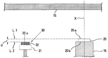
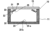
- FIG. 1A and 1B are explanatory views showing an outline of the configuration of the electron beam excitation light source according to the first embodiment of the present invention, where FIG. 1A is a side sectional view, and FIG. It is a top view which shows a state.
- This electron beam excitation type light source has a vacuum container 10 whose outer shape is sealed with a negative pressure inside and has a rectangular parallelepiped shape, and this vacuum container 10 has an opening on one side (the upper surface in FIG. 1A).
- a container base 11 and a light transmission window 15 disposed in the opening of the container base 11 and hermetically sealed to the container base 11 are configured.
- a semiconductor light emitting element 20 is arranged such that its surface (upper surface in FIG. 1A) 20a faces the light transmission window 15 apart from the light transmitting window 15.
- a planar electron beam emitting portion 32 is formed on the support substrate 31 in a region close to the semiconductor light emitting device 20 other than a region on the front surface 20 a and a region on the back surface 20 b of the semiconductor light emitting device 20.
- the electron beam source 30 is arranged so as to surround the semiconductor light emitting element 20.
- the electron beam source 30 is formed of an annular belt-like body, and the surface 32a from which the electron beam is emitted in the electron beam emitting portion 32 is oriented in the same direction as the surface 20a of the semiconductor light emitting element 20, that is, a vacuum.
- the container 10 is disposed so as to surround the semiconductor light emitting element 20 in a posture facing the light transmission window 15. In this state, the container 10 is fixed to the bottom wall of the container base 11 in the vacuum container 10 via the support member 37.
- the semiconductor light emitting element 20 and the electron beam source 30 are electrons provided to the outside of the vacuum vessel 10 for applying an acceleration voltage via a conductive wire (not shown) drawn from the inside of the vacuum vessel 10 to the outside. It is electrically connected to acceleration means (not shown). Further, the semiconductor light emitting element 20 is fixed to the bottom wall of the container base 11 in the vacuum container 10 through the high heat conductive member 16 provided on the back surface 20b.
- an insulator such as glass such as quartz glass and ceramics such as alumina can be used.
- transmit the light from the semiconductor light-emitting device 20 is used, For example, quartz glass, sapphire, etc. can be used.
- the pressure inside the vacuum vessel 10 is, for example, 10 ⁇ 4 to 10 ⁇ 6 Pa.
- An example of the dimensions of the vacuum container 10 is that the outer dimensions of the container base 11 are 40 mm ⁇ 40 mm ⁇ 20 mm, the thickness of the container base 11 is 2 mm, the opening of the container base 11 is 36 mm ⁇ 36 mm, and the light transmission window 15 The dimensions are 40 mm ⁇ 40 mm ⁇ 2 mm.
- a metal having high thermal conductivity such as copper or diamond can be used.
- the semiconductor light emitting element 20 is formed on a substrate 21 made of, for example, sapphire, a buffer layer 22 made of, for example, AlN formed on one surface of the substrate 21, and on one surface of the buffer layer 22.
- the active layer 25 has a single quantum well structure or a multiple quantum well structure.
- the substrate 21 is bonded to the high thermal conductive member 16 by brazing or the like with the active layer 25 facing the light transmission window 15 in the vacuum vessel 10.
- the thickness of the substrate 21 is, for example, 10 to 1000 ⁇ m
- the thickness of the buffer layer 22 is, for example, 100 to 1000 nm.
- the distance between the active layer 25 and the electron beam source 30 in the semiconductor light emitting device 20 is, for example, 5 to 15 mm. Further, the distance between the light emitting surface 20a of the semiconductor light emitting element 20 and the inner surface of the light transmission window 15 is, for example, 3 to 25 mm.
- the active layer 25 is a single quantum well structure or a multiple quantum well structure consisting of each In x Al y Ga 1-xy N (0 ⁇ x ⁇ 1,0 ⁇ y ⁇ 1, x + y ⁇ 1), a single or A plurality of quantum well layers 26 and a single or a plurality of barrier layers 27 are alternately stacked on the buffer layer 22 in this order.
- the thickness of each quantum well layer 26 is, for example, 0.5 to 50 nm.
- the barrier layer 27 has a composition selected such that the forbidden band width is larger than that of the quantum well layer 26.
- AlN may be used, and each thickness is larger than the well width of the quantum well layer 26.
- a large value is set, specifically, for example, 1 to 100 nm.
- the period of the quantum well layer 26 constituting the active layer 25 is appropriately set in consideration of the total thickness of the quantum well layer 26, the barrier layer 27 and the active layer 25, the acceleration voltage of the electron beam used, etc. 1 to 100.
- the semiconductor light emitting element 20 can be formed by, for example, MOCVD (metal organic chemical vapor deposition). Specifically, by using a carrier gas composed of hydrogen and nitrogen and a source gas composed of trimethylaluminum and ammonia, vapor deposition is performed on the (0001) plane of the sapphire substrate 21 to have a required thickness. After forming the buffer layer 22 made of AlN, vapor phase growth is performed on the buffer layer 22 using a carrier gas made of hydrogen gas and nitrogen gas and a source gas made of trimethylaluminum, trimethylgallium, trimethylindium and ammonia.
- MOCVD metal organic chemical vapor deposition
- the active layer 25 having a single quantum well structure or a multiple quantum well structure made of Inx Aly Ga1-xy N (0 ⁇ x ⁇ 1, 0 ⁇ y ⁇ 1, x + y ⁇ 1) having a required thickness is formed.
- the semiconductor light emitting element 20 can be formed.
- each step of forming the buffer layer 22, the quantum well layer 26, and the barrier layer 27 conditions such as a processing temperature, a processing pressure, and a growth rate of each layer are determined according to the buffer layer 22, the quantum well layer 26, and the barrier layer 27 to be formed. It can set suitably according to a composition, thickness, etc. of this.
- a processing temperature when forming the quantum well layer 26 made of InAlGaN, trimethylindium is used as a source gas in addition to the above, and the processing temperature is set lower than when the quantum well layer 26 made of AlGaN is formed. That's fine.
- the method for forming the semiconductor multilayer film is not limited to the MOCVD method, and for example, an MBE method (molecular beam epitaxy method) or the like can also be used.
- the electron beam emitter 32 in the electron beam source 30 is formed by supporting a large number of carbon nanotubes on a support substrate 31, and the support substrate 31 in the electron beam source 30 is It is fixed on a plate-like base 33.
- a net-like extraction electrode 35 for emitting electrons from the electron beam emitting unit 32 is disposed above the surface 32a from which the electron beam is emitted in the electron beam emitting unit 32 of the electron beam source 30.
- the lead electrode 35 is fixed to the base 33 via an electrode holding member 36.
- the support substrate 31 and the extraction electrode 35 are connected to the electron beam emission power source 51 provided outside the vacuum vessel 10 via a conductive wire (not shown) drawn from the inside of the vacuum vessel 10 to the outside. Are electrically connected so that the positive electrode and the support substrate 31 become the negative electrode.
- the area of the surface 32a where the electron beam is emitted from the electron beam emitter 32 is preferably larger than the area of the surface 20a where the electron beam is incident on the semiconductor light emitting device 20.
- the area of the surface 20a of the electron beam in the semiconductor light emitting element 20 is incident as S 1, when the area of the surface 32a of the electron beam in an electron beam emitting unit 32 is radiated to the S 2, the ratio S 2 / S 1 is preferably 6 or more, more preferably 10 to 30.
- FIG. 4 shows that an electron beam is emitted from the electron beam source 30 to the semiconductor light emitting device 20 under the condition that the amount of electrons emitted from the electron beam emitting portion 32 is 10 mA / cm 2 and the power efficiency of the semiconductor light emitting device 20 is 20%.
- irradiation is a graph showing the relationship between the acceleration voltage required for obtaining the light output of the ratio S 2 / S 1 and 1W.
- the acceleration voltage required to obtain the output of 1 W light is inversely proportional to the ratio S 2 / S 1 , and the electron beam emission with respect to the area S 1 of the surface 20 a of the semiconductor light emitting device 20 is achieved.
- the acceleration voltage can be set lower as the ratio S 2 / S 1 of the area S 2 of the surface 32a of the portion 32 is larger. This is considered to be because the electron density of the electron beam emitted from the electron beam emitting portion 32 increases in proportion to the ratio S 2 / S 1 when entering the surface 20 a of the semiconductor light emitting device 20. It is done.
- the outer diameter of the support substrate 31 is 25 mm
- the inner diameter is 19 mm
- the thickness is 0.1 mm
- the outer diameter of the electron beam emitting portion 32 is 24 mm
- the inner diameter is 20 mm
- the thickness is 0.
- the area of the surface from which the electron beam is emitted in the electron beam emitting portion 32 is 138 mm 2 .
- a metal material containing iron, nickel, cobalt, or chromium can be used as a material constituting the support substrate 31 .
- a method for forming the electron beam emitting portion 32 made of carbon nanotubes on the support substrate 31 is not particularly limited, and a known method can be used.
- the support substrate 31 having a metal catalyst layer formed on the surface is heated.
- a carbon source gas such as CO or acetylene
- a screen printing method or the like in which a paste containing carbon nanotube powder and an organic binder in a liquid medium is prepared, and this paste is applied to the surface of the support substrate 31 by screen printing and dried. it can.
- a metal material containing any of iron, nickel, cobalt, and chromium can be used as a material constituting the extraction electrode 35.
- the electron beam excitation light source when a voltage is applied between the electron beam source 30 and the extraction electrode 35, electrons are emitted from the electron beam emitting portion 32 of the electron beam source 30 toward the extraction electrode 35.
- the electrons travel while being accelerated toward the semiconductor light emitting element 20 by an acceleration voltage applied between the semiconductor light emitting element 20 and the electron beam source 30 and are converted into an electron beam on the surface 20a of the semiconductor light emitting element 20, that is, the activity. Incident on the surface of the layer 25.
- the semiconductor light emitting device 20 electrons in the active layer 25 are excited by the incidence of the electron beam, and as a result, light such as ultraviolet rays is emitted from the surface 20 a on which the electron beam in the semiconductor light emitting device 20 is incident. Then, the light is emitted to the outside of the vacuum vessel 10 through the light transmission window 15 in the vacuum vessel 10.
- the amount of electrons emitted from the electron beam emitting portion 32 is preferably 25 mA / cm 2 or less, more preferably 1 to 15 mA / cm 2 , and particularly preferably 5 to 10 mA / cm 2 .
- the amount of emitted electrons exceeds 25 mA / cm 2 , it is necessary to considerably increase the voltage applied to the electron beam source 30. As a result, the electron beam source 30 generates heat and causes an early failure. , May arise.
- the amount of electron beam radiation is too small, a sufficient amount of electron beam is not irradiated onto the surface 20a of the semiconductor light emitting element 20, and it may be difficult to obtain a high light output.
- the voltage applied between the electron beam source 30 and the extraction electrode 35 is preferably 1 to 5 kV. If this voltage is too low, the electron density of the electron beam emitted from the electron beam emitting section 32 is small, and it may be difficult to obtain a high light output. On the other hand, if this voltage is excessive, the electron beam source 30 may generate heat and cause a failure at an early stage.
- the acceleration voltage of the electron beam is preferably 6 to 12 kV. When the acceleration voltage is too small, electrons emitted from the electron beam emitting portion 32 are not sufficiently accelerated, and it may be difficult to obtain a high light output. On the other hand, if the acceleration voltage is excessive, X-rays are likely to be generated from the semiconductor light emitting element 20, and the semiconductor light emitting element 20 is easily damaged by the energy of the electron beam, which is not preferable.
- the electron beam source 30 formed of an annular belt having a planar electron beam emitting portion 32 surrounds the semiconductor light emitting element 20 around the semiconductor light emitting element 20.
- the surface 20a of the semiconductor light emitting element 20 can be uniformly irradiated with an electron beam, and a high light output can be obtained without increasing the acceleration voltage of the electron beam.
- the semiconductor light emitting device 20 is connected to the semiconductor light emitting device 20 from the back surface 20b via the high thermal conductive member 16. It is possible to cool. Therefore, since the semiconductor light emitting element 20 can be efficiently cooled, the light emission efficiency of the semiconductor light emitting element 20 is not lowered and high output light is maintained.
- the amount of electrons emitted from the electron beam emitter 32 is set to 25 mA / cm 2 or less, a high light output can be obtained without increasing the voltage applied to the electron beam source 30.
- the area of the surface 32a from which the electron beam is emitted in the electron beam emitting portion 32 is larger than the area of the surface 20a to which the electron beam is incident in the semiconductor light emitting device 20, the electrons emitted from the electron beam emitting portion 32. Since the line has a high electron density when incident on the surface 20a of the semiconductor light emitting device 20, a higher light output can be obtained without increasing the acceleration voltage.
- FIGS. 5A and 5B are explanatory views showing an outline of the configuration of the electron beam excitation light source according to the second embodiment of the present invention, in which FIG. 5A is a side sectional view and FIG. 5B is a light transmission window removed. It is a top view which shows a state.
- this electron beam excitation light source a plurality of (four in the illustrated example) electron beams each having a planar electron beam emitting portion 32 formed on a support substrate 31 in the peripheral region of the semiconductor light emitting element 20.
- a source 30 is arranged so as to surround the semiconductor light emitting element 20.
- each of the electron beam sources 30 is formed of a partially annular belt-like body, and the surface 32a from which the electron beam is emitted in the electron beam emitting portion 32 faces the same direction as the surface 20a of the semiconductor light emitting element 20. It is arranged to surround the semiconductor light emitting element 20 along a circle centered on the semiconductor light emitting element 20 in an attitude, that is, an attitude facing the light transmission window 15 of the vacuum vessel 10, and in this state, the vacuum is passed through the support member 37.
- the container 10 is fixed to the bottom wall of the container base 11.
- Other specific configurations are the same as those of the electron beam excitation light source according to the first embodiment.
- a plurality of electron beam sources 30 each having a planar electron beam emitting portion 32 and made of a partially annular belt-like body are disposed around the semiconductor light emitting element 20. Since the surface 20a of the semiconductor light emitting device 20 is uniformly irradiated with the electron beam, a high light output can be obtained without increasing the acceleration voltage of the electron beam. Moreover, since light is emitted from the front surface 20a of the semiconductor light emitting device 20 on which the electron beam from the electron beam source 30 is incident, the semiconductor light emitting device 20 is connected to the semiconductor light emitting device 20 from the back surface 20b via the high thermal conductive member 16. It is possible to cool. Therefore, since the semiconductor light emitting element 20 can be efficiently cooled, the light emission efficiency of the semiconductor light emitting element 20 is not lowered and high output light is maintained.
- FIG. 6A and 6B are explanatory views showing an outline of the configuration of the electron beam excitation light source according to the third embodiment of the present invention, in which FIG. 6A is a side sectional view, and FIG. It is a top view which shows a state.
- the semiconductor light emitting element 20 is disposed on the inner surface of the bottom wall of the container base 11 in the vacuum container 10, and the surface (the upper surface in FIG. 6A) 20 a is separated from the light transmission window 15.
- a plurality of (two in the illustrated example) are formed by forming rectangular planar electron beam emitting portions 32 on a rectangular support substrate 31, respectively.
- the electron beam source 30 is disposed at a position sandwiching the semiconductor light emitting element 20.
- the electron beam emitter 32 in each of the electron beam sources 30 is formed by supporting a large number of carbon nanotubes on the support substrate 31, and the support substrate 31 in each of the electron beam sources 30 is
- Each of the electron beam sources 30 fixes the semiconductor light emitting element 20 by fixing each base plate 33 to the inner surfaces of two opposite side walls of the container base 11.
- the electron beam emitting portions 32 are arranged so as to face each other at the sandwiched position.
- Other specific configurations are the same as those of the electron beam excitation light source according to the first embodiment.
- a plurality of electron beam sources 30 having a planar electron beam emitting portion 32 are arranged at a position sandwiching the semiconductor light emitting element 20 around the semiconductor light emitting element 20. Therefore, the surface 20a of the semiconductor light emitting element 20 can be uniformly irradiated with an electron beam, and a high light output can be obtained without increasing the acceleration voltage of the electron beam. Moreover, since light is emitted from the front surface 20a of the semiconductor light emitting device 20 on which the electron beam from the electron beam source 30 is incident, the semiconductor light emitting device 20 can be cooled from the back surface 20b of the semiconductor light emitting device 20. . Therefore, since the semiconductor light emitting element 20 can be efficiently cooled, the light emission efficiency of the semiconductor light emitting element 20 is not lowered and high output light is maintained. *
- FIGS. 7A and 7B are explanatory views showing an outline of the configuration of the electron beam excitation light source according to the fourth embodiment of the present invention, where FIG. 7A is a side sectional view and FIG. 7B is a light transmission window removed. It is a top view which shows a state.
- This electron beam excitation type light source has a vacuum container 10 whose outer shape is sealed in a negative pressure state and has a rectangular parallelepiped shape, and this vacuum container 10 has an opening on one side (the upper surface in FIG. 7A).
- a container base 11 and a light transmission window 15 disposed in the opening of the container base 11 and hermetically sealed to the container base 11 are configured.
- a semiconductor light emitting element 20 is arranged such that its surface (upper surface in FIG. 7A) 20a faces the light transmission window 15 with a space therebetween, and a peripheral region of the semiconductor light emitting element 20, specifically, Specifically, a planar electron beam emitting portion 32 is formed on the support substrate 31 in a region close to the semiconductor light emitting device 20 other than a region on the front surface 20 a and a region on the back surface 20 b of the semiconductor light emitting device 20.
- the electron beam source 30 is arranged so as to surround the semiconductor light emitting element 20.
- the electron beam source 30 is formed of an annular belt-like body, and the surface 32a from which the electron beam is emitted in the electron beam emitting portion 32 is oriented in the same direction as the surface 20a of the semiconductor light emitting element 20, that is, a vacuum.
- the container 10 is disposed so as to surround the semiconductor light emitting element 20 in a posture facing the light transmission window 15. In this state, the container 10 is fixed to the bottom wall of the container base 11 in the vacuum container 10 via the support member 37.
- the semiconductor light emitting element 20 and the electron beam source 30 are connected to an electron accelerating means 50 for applying an accelerating voltage provided outside the vacuum vessel 10 through a conductive wire drawn from the inside of the vacuum vessel 10 to the outside.
- the semiconductor light emitting device 20 is electrically connected so as to be a positive electrode and the electron beam source 30 is a negative electrode.
- the semiconductor light emitting element 20 is fixed to the bottom wall of the container base 11 in the vacuum container 10 via the high thermal conductive member 16 provided on the back surface 20b.
- Specific configurations of the vacuum vessel 10, the semiconductor light emitting element 20, and the electron beam source 30 are the same as those of the electron beam excitation light source according to the first embodiment.
- the orbit of the electron beam emitted from the electron beam source 30 is directed toward the surface 20 a from which light is emitted in the semiconductor light emitting device 20 at a position outside the electron beam source 30 with respect to the semiconductor light emitting device 20.
- An electric field control electrode 40 is disposed.
- the electric field control electrode 40 has a barrel portion 41 having an inner diameter larger than the outer diameter of the electron beam source 30, and a tip (the upper end in FIG. 7A) formed continuously with the barrel portion 41. ) And is arranged so as to surround the outer periphery of the electron beam source 30, and the base end of the electric field control electrode 40 is the container base 11 in the vacuum container 10. It is fixed to the bottom wall.
- the electron beam source 30 and the electric field control electrode 40 are connected to the electric field control power source 52 provided outside the vacuum vessel 10 via a conductive wire drawn from the inside of the vacuum vessel 10 to the outside.
- the positive electrode and the electric field control electrode 40 are electrically connected to be a negative electrode.
- the level L1 of the surface 20 a on which the electron beam in the semiconductor light emitting element 20 is incident is the electron beam emission of the electron beam source 30.
- the electric field control electrode 40 As a material constituting the electric field control electrode 40, a metal material containing any of iron, nickel, cobalt, chromium, aluminum, silver, copper, titanium, and zirconium can be used.
- An example of the dimensions of the electric field control electrode 40 is as follows.
- the inner diameter of the body 41 is 34 mm, the length in the axial direction is 12 mm, the inner diameter at the tip of the tapered portion 42 is 28 mm, the length in the axial direction is 3 mm, and the body 41
- the inclination of the taper portion 42 with respect to the surface is 45 °, for example, the thickness of the cylindrical body constituting the electric field control electrode 40 is 0.3 mm, and the surface of the electron beam emitting portion 32 of the electron beam source 30 where the electron beam is emitted
- the distance between the level and the level of the tip of the tapered portion 42 is 7 mm.
- the electron beam excitation light source when a voltage is applied between the electron beam source 30 and the extraction electrode 35, electrons are emitted from the electron beam emitting portion 32 of the electron beam source 30 toward the extraction electrode 35.
- the electrons are accelerated toward the semiconductor light emitting device 20 by an acceleration voltage applied between the semiconductor light emitting device 20 and the electron beam source 30, and an electron beam is formed.
- the voltage applied between the electron beam source 30 and the electric field control electrode 40 by the acceleration voltage and the electric field control power source 52 is directed toward the surface 20a where the light in the semiconductor light emitting element 20 is emitted, and as a result.
- the electron beam is incident on the surface 20 a of the semiconductor light emitting device 20, that is, the surface of the active layer 25.
- the semiconductor light emitting device 20 electrons in the active layer 25 are excited by the incidence of the electron beam, and as a result, light such as ultraviolet rays is emitted from the surface 20 a on which the electron beam in the semiconductor light emitting device 20 is incident. Then, the light is emitted to the outside of the vacuum vessel 10 through the light transmission window 15 in the vacuum vessel 10.
- the voltage applied between the electron beam source 30 and the extraction electrode 35 by the electron beam emission power source 51 is preferably 1 to 5 kV.
- the acceleration voltage of the electron beam applied by the electron acceleration means 50 is preferably 6 to 12 kV.
- the voltage applied between the electron beam source 30 and the electric field control electrode 40 by the electric field control power supply 52 is, for example, ⁇ 2 to 2 kV.
- the amount of electrons emitted from the electron beam emitter 32 is preferably 25 mA / cm 2 or less, more preferably 1 to 15 mA / cm 2 , and particularly preferably 5 to 10 mA / cm 2 .
- the electric field control electrode 40 directs the orbit of the electron beam emitted from the electron beam source 30 toward the surface 20a where the light in the semiconductor light emitting element 20 is emitted. Therefore, an electron beam can be incident on the surface 20a of the semiconductor light emitting element 20 with high efficiency, and a high light output can be obtained without increasing the acceleration voltage of the electron beam. Moreover, since light is emitted from the front surface 20a of the semiconductor light emitting device 20 on which the electron beam from the electron beam source 30 is incident, the semiconductor light emitting device 20 is connected to the semiconductor light emitting device 20 from the back surface 20b via the high thermal conductive member 16. It is possible to cool.
- the electron beam source 30 is formed of an annular band having a planar electron beam emitting portion 32, and the electron beam source 30 is arranged so as to surround the semiconductor light emitting element 20 around the semiconductor light emitting element 20. Therefore, the surface 20a of the semiconductor light emitting element 20 can be uniformly irradiated with an electron beam.
- the amount of electrons emitted from the electron beam emitter 32 is set to 25 mA / cm 2 or less, a high light output can be obtained without increasing the voltage applied to the electron beam source 30.
- the area of the surface 32a from which the electron beam is emitted in the electron beam emitting portion 32 is larger than the area of the surface 20a to which the electron beam is incident in the semiconductor light emitting device 20, the electrons emitted from the electron beam emitting portion 32. Since the line has a high electron density when incident on the surface 20a of the semiconductor light emitting device 20, a higher light output can be obtained without increasing the acceleration voltage.
- FIG. 9 is an explanatory diagram showing an outline of the configuration of an electron beam excitation light source according to a fifth embodiment of the present invention, where (a) is a side sectional view and (b) is a light transmission window removed. It is a top view which shows a state.
- this electron beam excitation light source a plurality of (four in the illustrated example) electron beams each having a planar electron beam emitting portion 32 formed on a support substrate 31 in the peripheral region of the semiconductor light emitting element 20.
- a source 30 is arranged so as to surround the semiconductor light emitting element 20.
- each of the electron beam sources 30 is formed of a partially annular belt-like body, and the surface 32a from which the electron beam is emitted in the electron beam emitting portion 32 faces the same direction as the surface 20a of the semiconductor light emitting element 20. It is arranged to surround the semiconductor light emitting element 20 along a circle centered on the semiconductor light emitting element 20 in an attitude, that is, an attitude facing the light transmission window 15 of the vacuum vessel 10, and in this state, the vacuum is passed through the support member 37.
- the container 10 is fixed to the bottom wall of the container base 11.
- each of the electric field control electrodes 40 is formed of a partial cylindrical body, and has a body 41 having an inner surface with a radius of curvature larger than the radius of curvature of the outer surface of the electron beam source 30, and the body 41 continuously.
- the formed tapered portion 42 having a radius of curvature that decreases toward the tip (upper end in FIG.
- the electron beam source 30 and the electric field control electrode 40 are connected to the electric field control power source 52 provided outside the vacuum vessel 10 via a conductive wire drawn from the inside of the vacuum vessel 10 to the outside.
- the positive electrode and the electric field control electrode 40 are electrically connected to be a negative electrode.
- Other specific configurations are the same as those of the electron beam excitation light source according to the fourth embodiment.
- each electric field control electrode 40 directs the trajectory of the electron beam emitted from each electron beam source 30 toward the surface 20a where the light in the semiconductor light emitting element 20 is emitted. Therefore, an electron beam can be incident on the surface 20a of the semiconductor light emitting element 20 with high efficiency, and a high light output can be obtained without increasing the acceleration voltage of the electron beam.
- the semiconductor light emitting device 20 since light is emitted from the front surface 20 a on which the electron beam from each electron beam source 30 in the semiconductor light emitting device 20 is incident, the semiconductor light emitting device 20 from the back surface 20 b of the semiconductor light emitting device 20 through the high thermal conductive member 16. Can be cooled.
- each of the electron beam sources 30 is formed of a partially annular belt having a planar electron beam emitting portion 32, and these electron beam sources 30 are arranged around the semiconductor light emitting element 20 to connect the semiconductor light emitting element 20. Since they are arranged so as to surround them, the surface 20a of the semiconductor light emitting element 20 can be uniformly irradiated with an electron beam.
- the electron beam source of the present invention is not particularly limited as long as it has a planar electron beam emitting portion.
- the electron beam source is not limited to a rectangular plate shape or other shapes. It may be.
- the arrangement position of the electron beam source is not particularly limited as long as the electron beam source is positioned around the semiconductor light emitting element and can enter the electron beam on the light emitting surface of the semiconductor light emitting element.
- the electron beam excitation type light source according to the third embodiment as shown in FIG.
- the electron beam source 30 has an electron beam emitting portion 32 at the semiconductor light emitting element 20 at a position sandwiching the semiconductor light emitting element 20. It may be arranged to face. Moreover, the electron beam emission part 32 in the electron beam source 30 is not limited to what consists of carbon nanotubes, The thing of various structures can be used if it is planar.
- the electric field control electrode 40 it is not essential to form the taper portion 42 in the electric field control electrode 40.
- the outer diameter and the inner diameter are uniform in the axial direction in a cylindrical shape. It may be.
- the electric field control electrode 40 may be composed of a first electrode member 40a and a second electrode member 40b which are divided vertically. In the electric field control electrode 40 having such a configuration, it is preferable that a voltage higher than that of the lower first electrode member 40a is applied to the upper second electrode member 40b.
- the trajectory of the emitted electron beam can be reliably directed toward the surface 20a from which light is emitted from the semiconductor light emitting device 20, and as a result, the electron beam is incident on the surface 20a of the semiconductor light emitting device 20 with higher efficiency. can do.
- the electric field control electrode 40 may be disposed at a position inward of the electron beam source 30 with respect to the semiconductor light emitting element 20. In this case, a positive voltage is applied to the electron beam source 30. Is done.
- the electric field control electrode 40 is disposed outside the electron beam source 30 with respect to the semiconductor light emitting element 20 in that an electron beam can be incident on the semiconductor light emitting element 20 with high efficiency. It is preferable.
Abstract
Le but de l'invention est de fournir une source de lumière pompée à faisceau d'électrons qui permette d'irradier uniformément une surface d'un élément émetteur de lumière à semi-conducteur avec des faisceaux d'électrons, qui permette d'obtenir une sortie de lumière élevée sans augmenter la tension d'accélération des faisceaux d'électrons, et qui permette de refroidir efficacement l'élément émetteur de lumière à semi-conducteur. Cette source de lumière pompée à faisceau d'électrons comprend une source de faisceaux d'électrons et un élément émetteur de lumière à semi-conducteur qui est excité par les faisceaux d'électrons émis par la source de faisceaux d'électrons. La source de lumière pompée à faisceau d'électrons est caractérisée en ce que : la source de faisceaux d'électrons possède une partie émettrice de faisceaux d'électrons plane et est disposée autour de l'élément émetteur de lumière à semi-conducteur ; et la lumière est émise depuis une surface de l'élément émetteur de lumière à semi-conducteur, le faisceau d'électrons provenant de la source de faisceaux d'électrons étant incident sur cette surface.
Priority Applications (1)
| Application Number | Priority Date | Filing Date | Title |
|---|---|---|---|
| US13/884,820 US9184559B2 (en) | 2010-11-10 | 2011-10-11 | Electron-beam-pumped light source |
Applications Claiming Priority (6)
| Application Number | Priority Date | Filing Date | Title |
|---|---|---|---|
| JP2010-251682 | 2010-11-10 | ||
| JP2010251682A JP5299405B2 (ja) | 2010-11-10 | 2010-11-10 | 電子線励起型光源 |
| JP2010251684A JP5736736B2 (ja) | 2010-11-10 | 2010-11-10 | 電子線励起型光源 |
| JP2010251683A JP5659712B2 (ja) | 2010-11-10 | 2010-11-10 | 電子線励起型光源 |
| JP2010-251684 | 2010-11-10 | ||
| JP2010-251683 | 2010-11-10 |
Publications (1)
| Publication Number | Publication Date |
|---|---|
| WO2012063585A1 true WO2012063585A1 (fr) | 2012-05-18 |
Family
ID=46050738
Family Applications (1)
| Application Number | Title | Priority Date | Filing Date |
|---|---|---|---|
| PCT/JP2011/073292 WO2012063585A1 (fr) | 2010-11-10 | 2011-10-11 | Source de lumière pompée à faisceau d'électrons |
Country Status (3)
| Country | Link |
|---|---|
| US (1) | US9184559B2 (fr) |
| TW (1) | TWI520455B (fr) |
| WO (1) | WO2012063585A1 (fr) |
Cited By (1)
| Publication number | Priority date | Publication date | Assignee | Title |
|---|---|---|---|---|
| WO2013145915A1 (fr) * | 2012-03-29 | 2013-10-03 | ウシオ電機株式会社 | Dispositif d'émission uv à excitation par faisceau d'électrons |
Families Citing this family (3)
| Publication number | Priority date | Publication date | Assignee | Title |
|---|---|---|---|---|
| US10056735B1 (en) * | 2016-05-23 | 2018-08-21 | X Development Llc | Scanning UV light source utilizing semiconductor heterostructures |
| CN112595703B (zh) * | 2020-12-09 | 2023-04-18 | 中国科学院云南天文台 | 电子束激发半导体发光性能测试平台和激发参数优化方法 |
| CN112557863B (zh) * | 2020-12-09 | 2023-05-02 | 中国科学院云南天文台 | 一种载流子转换效率测量平台和方法 |
Citations (6)
| Publication number | Priority date | Publication date | Assignee | Title |
|---|---|---|---|---|
| JPH0496281A (ja) * | 1990-08-03 | 1992-03-27 | Kawasaki Steel Corp | 半導体発光装置 |
| JPH09214027A (ja) * | 1996-02-01 | 1997-08-15 | Matsushita Electric Ind Co Ltd | 電子線励起レーザ装置 |
| JP2001015840A (ja) * | 1999-07-02 | 2001-01-19 | Agency Of Ind Science & Technol | ガス励起装置 |
| JP2006261150A (ja) * | 2005-03-15 | 2006-09-28 | Ricoh Co Ltd | 垂直共振器型面発光半導体レーザ装置および発光システムおよび光伝送システム |
| JP2006287028A (ja) * | 2005-04-01 | 2006-10-19 | Shinichi Hirabayashi | レーザー発光構造体 |
| WO2007023832A1 (fr) * | 2005-08-24 | 2007-03-01 | National Institute For Materials Science | Émetteur de lumière à l’oxyde de zinc et dispositif émetteur de lumière |
Family Cites Families (9)
| Publication number | Priority date | Publication date | Assignee | Title |
|---|---|---|---|---|
| FR2661566B1 (fr) * | 1990-04-25 | 1995-03-31 | Commissariat Energie Atomique | Laser compact a semi-conducteur du type a pompage electronique. |
| JP3667188B2 (ja) | 2000-03-03 | 2005-07-06 | キヤノン株式会社 | 電子線励起レーザー装置及びマルチ電子線励起レーザー装置 |
| US7309953B2 (en) * | 2005-01-24 | 2007-12-18 | Principia Lightworks, Inc. | Electron beam pumped laser light source for projection television |
| US20070036194A1 (en) * | 2005-08-15 | 2007-02-15 | Govorkov Sergei V | Excimer-lamp pumped semiconductor laser |
| US7737392B2 (en) * | 2006-11-09 | 2010-06-15 | The Board Of Trustees Of The University Of Illinois | Photonic crystal sensors with integrated fluid containment structure, sample handling devices incorporating same, and uses thereof for biomolecular interaction analysis |
| WO2008091844A2 (fr) * | 2007-01-22 | 2008-07-31 | Principia Lightworks, Inc. | Dalle laser à cavité verticale avec réseau de diffraction |
| US20130294467A1 (en) * | 2007-10-15 | 2013-11-07 | Jerome V. Moloney | Laser-based source for terahertz and millimeter waves |
| US7756175B2 (en) * | 2008-10-30 | 2010-07-13 | The United States Of America As Represented By The Secretary Of The Army | Pumped semiconductor laser systems and methods |
| CA2773264A1 (fr) * | 2009-09-07 | 2011-03-10 | Shingo Ono | Dispositif permettant d'emettre un rayonnement ultraviolet du vide |
-
2011
- 2011-10-11 US US13/884,820 patent/US9184559B2/en not_active Expired - Fee Related
- 2011-10-11 WO PCT/JP2011/073292 patent/WO2012063585A1/fr active Application Filing
- 2011-10-27 TW TW100139177A patent/TWI520455B/zh not_active IP Right Cessation
Patent Citations (6)
| Publication number | Priority date | Publication date | Assignee | Title |
|---|---|---|---|---|
| JPH0496281A (ja) * | 1990-08-03 | 1992-03-27 | Kawasaki Steel Corp | 半導体発光装置 |
| JPH09214027A (ja) * | 1996-02-01 | 1997-08-15 | Matsushita Electric Ind Co Ltd | 電子線励起レーザ装置 |
| JP2001015840A (ja) * | 1999-07-02 | 2001-01-19 | Agency Of Ind Science & Technol | ガス励起装置 |
| JP2006261150A (ja) * | 2005-03-15 | 2006-09-28 | Ricoh Co Ltd | 垂直共振器型面発光半導体レーザ装置および発光システムおよび光伝送システム |
| JP2006287028A (ja) * | 2005-04-01 | 2006-10-19 | Shinichi Hirabayashi | レーザー発光構造体 |
| WO2007023832A1 (fr) * | 2005-08-24 | 2007-03-01 | National Institute For Materials Science | Émetteur de lumière à l’oxyde de zinc et dispositif émetteur de lumière |
Cited By (1)
| Publication number | Priority date | Publication date | Assignee | Title |
|---|---|---|---|---|
| WO2013145915A1 (fr) * | 2012-03-29 | 2013-10-03 | ウシオ電機株式会社 | Dispositif d'émission uv à excitation par faisceau d'électrons |
Also Published As
| Publication number | Publication date |
|---|---|
| US9184559B2 (en) | 2015-11-10 |
| TWI520455B (zh) | 2016-02-01 |
| US20130322484A1 (en) | 2013-12-05 |
| TW201238189A (en) | 2012-09-16 |
Similar Documents
| Publication | Publication Date | Title |
|---|---|---|
| US9934926B2 (en) | Activation chamber, kit used in treatment device and treatment device, for lowering electron affinity | |
| US9306090B2 (en) | Composite particle, composite particle dispersion, and photovoltaic device, | |
| WO2012063585A1 (fr) | Source de lumière pompée à faisceau d'électrons | |
| JP6454017B2 (ja) | 電界放出光源 | |
| TWI427665B (zh) | X射線電子束產生器及其陰極 | |
| JP2007258119A (ja) | スピン偏極電子発生装置 | |
| JP5192097B2 (ja) | 紫外線照射装置 | |
| JP5736736B2 (ja) | 電子線励起型光源 | |
| WO2013145915A1 (fr) | Dispositif d'émission uv à excitation par faisceau d'électrons | |
| JP5659712B2 (ja) | 電子線励起型光源 | |
| JP2009021032A (ja) | X線発生管 | |
| JP5370408B2 (ja) | 電子線励起型光源装置 | |
| JP5299405B2 (ja) | 電子線励起型光源 | |
| JP2013135035A (ja) | 電子線励起型光源装置 | |
| KR20210083040A (ko) | 엑스레이 튜브 | |
| JP2015046415A (ja) | 窒化物半導体発光素子および電子線励起型光源装置 | |
| JP2012209448A (ja) | 電子線励起型光源装置 | |
| KR102283035B1 (ko) | 전자빔 증폭형 초소형 엑스선 튜브 | |
| JP2012195144A (ja) | 電子線源装置および電子線励起型光源装置 | |
| JP2012212637A (ja) | 電子線源装置および電子線励起型光源装置 | |
| JP2013033640A (ja) | 電子線励起型光源装置 | |
| JP2013149716A (ja) | 真空容器装置 | |
| JP2013222648A (ja) | 電子線放射装置 | |
| JP2006090873A (ja) | 電子線透過窓、その製造方法及び電子線照射装置 | |
| JP2014049591A (ja) | 電子線励起型光源 |
Legal Events
| Date | Code | Title | Description |
|---|---|---|---|
| 121 | Ep: the epo has been informed by wipo that ep was designated in this application |
Ref document number: 11839818 Country of ref document: EP Kind code of ref document: A1 |
|
| NENP | Non-entry into the national phase |
Ref country code: DE |
|
| WWE | Wipo information: entry into national phase |
Ref document number: 13884820 Country of ref document: US |
|
| 122 | Ep: pct application non-entry in european phase |
Ref document number: 11839818 Country of ref document: EP Kind code of ref document: A1 |