WO2012053466A1 - 表示装置およびその駆動方法 - Google Patents
表示装置およびその駆動方法 Download PDFInfo
- Publication number
- WO2012053466A1 WO2012053466A1 PCT/JP2011/073797 JP2011073797W WO2012053466A1 WO 2012053466 A1 WO2012053466 A1 WO 2012053466A1 JP 2011073797 W JP2011073797 W JP 2011073797W WO 2012053466 A1 WO2012053466 A1 WO 2012053466A1
- Authority
- WO
- WIPO (PCT)
- Prior art keywords
- shift
- unit
- signal
- period
- register
- Prior art date
- Legal status (The legal status is an assumption and is not a legal conclusion. Google has not performed a legal analysis and makes no representation as to the accuracy of the status listed.)
- Ceased
Links
Images










Classifications
-
- G—PHYSICS
- G09—EDUCATION; CRYPTOGRAPHY; DISPLAY; ADVERTISING; SEALS
- G09G—ARRANGEMENTS OR CIRCUITS FOR CONTROL OF INDICATING DEVICES USING STATIC MEANS TO PRESENT VARIABLE INFORMATION
- G09G3/00—Control arrangements or circuits, of interest only in connection with visual indicators other than cathode-ray tubes
- G09G3/20—Control arrangements or circuits, of interest only in connection with visual indicators other than cathode-ray tubes for presentation of an assembly of a number of characters, e.g. a page, by composing the assembly by combination of individual elements arranged in a matrix no fixed position being assigned to or needed to be assigned to the individual characters or partial characters
- G09G3/34—Control arrangements or circuits, of interest only in connection with visual indicators other than cathode-ray tubes for presentation of an assembly of a number of characters, e.g. a page, by composing the assembly by combination of individual elements arranged in a matrix no fixed position being assigned to or needed to be assigned to the individual characters or partial characters by control of light from an independent source
- G09G3/36—Control arrangements or circuits, of interest only in connection with visual indicators other than cathode-ray tubes for presentation of an assembly of a number of characters, e.g. a page, by composing the assembly by combination of individual elements arranged in a matrix no fixed position being assigned to or needed to be assigned to the individual characters or partial characters by control of light from an independent source using liquid crystals
- G09G3/3611—Control of matrices with row and column drivers
-
- G—PHYSICS
- G09—EDUCATION; CRYPTOGRAPHY; DISPLAY; ADVERTISING; SEALS
- G09G—ARRANGEMENTS OR CIRCUITS FOR CONTROL OF INDICATING DEVICES USING STATIC MEANS TO PRESENT VARIABLE INFORMATION
- G09G3/00—Control arrangements or circuits, of interest only in connection with visual indicators other than cathode-ray tubes
- G09G3/20—Control arrangements or circuits, of interest only in connection with visual indicators other than cathode-ray tubes for presentation of an assembly of a number of characters, e.g. a page, by composing the assembly by combination of individual elements arranged in a matrix no fixed position being assigned to or needed to be assigned to the individual characters or partial characters
- G09G3/34—Control arrangements or circuits, of interest only in connection with visual indicators other than cathode-ray tubes for presentation of an assembly of a number of characters, e.g. a page, by composing the assembly by combination of individual elements arranged in a matrix no fixed position being assigned to or needed to be assigned to the individual characters or partial characters by control of light from an independent source
- G09G3/36—Control arrangements or circuits, of interest only in connection with visual indicators other than cathode-ray tubes for presentation of an assembly of a number of characters, e.g. a page, by composing the assembly by combination of individual elements arranged in a matrix no fixed position being assigned to or needed to be assigned to the individual characters or partial characters by control of light from an independent source using liquid crystals
- G09G3/3611—Control of matrices with row and column drivers
- G09G3/3674—Details of drivers for scan electrodes
- G09G3/3677—Details of drivers for scan electrodes suitable for active matrices only
-
- G—PHYSICS
- G09—EDUCATION; CRYPTOGRAPHY; DISPLAY; ADVERTISING; SEALS
- G09G—ARRANGEMENTS OR CIRCUITS FOR CONTROL OF INDICATING DEVICES USING STATIC MEANS TO PRESENT VARIABLE INFORMATION
- G09G3/00—Control arrangements or circuits, of interest only in connection with visual indicators other than cathode-ray tubes
- G09G3/20—Control arrangements or circuits, of interest only in connection with visual indicators other than cathode-ray tubes for presentation of an assembly of a number of characters, e.g. a page, by composing the assembly by combination of individual elements arranged in a matrix no fixed position being assigned to or needed to be assigned to the individual characters or partial characters
- G09G3/34—Control arrangements or circuits, of interest only in connection with visual indicators other than cathode-ray tubes for presentation of an assembly of a number of characters, e.g. a page, by composing the assembly by combination of individual elements arranged in a matrix no fixed position being assigned to or needed to be assigned to the individual characters or partial characters by control of light from an independent source
- G09G3/36—Control arrangements or circuits, of interest only in connection with visual indicators other than cathode-ray tubes for presentation of an assembly of a number of characters, e.g. a page, by composing the assembly by combination of individual elements arranged in a matrix no fixed position being assigned to or needed to be assigned to the individual characters or partial characters by control of light from an independent source using liquid crystals
- G09G3/3611—Control of matrices with row and column drivers
- G09G3/3685—Details of drivers for data electrodes
- G09G3/3688—Details of drivers for data electrodes suitable for active matrices only
-
- G—PHYSICS
- G09—EDUCATION; CRYPTOGRAPHY; DISPLAY; ADVERTISING; SEALS
- G09G—ARRANGEMENTS OR CIRCUITS FOR CONTROL OF INDICATING DEVICES USING STATIC MEANS TO PRESENT VARIABLE INFORMATION
- G09G2310/00—Command of the display device
- G09G2310/02—Addressing, scanning or driving the display screen or processing steps related thereto
- G09G2310/0264—Details of driving circuits
- G09G2310/0283—Arrangement of drivers for different directions of scanning
-
- G—PHYSICS
- G09—EDUCATION; CRYPTOGRAPHY; DISPLAY; ADVERTISING; SEALS
- G09G—ARRANGEMENTS OR CIRCUITS FOR CONTROL OF INDICATING DEVICES USING STATIC MEANS TO PRESENT VARIABLE INFORMATION
- G09G2310/00—Command of the display device
- G09G2310/08—Details of timing specific for flat panels, other than clock recovery
-
- G—PHYSICS
- G09—EDUCATION; CRYPTOGRAPHY; DISPLAY; ADVERTISING; SEALS
- G09G—ARRANGEMENTS OR CIRCUITS FOR CONTROL OF INDICATING DEVICES USING STATIC MEANS TO PRESENT VARIABLE INFORMATION
- G09G2330/00—Aspects of power supply; Aspects of display protection and defect management
- G09G2330/02—Details of power systems and of start or stop of display operation
- G09G2330/021—Power management, e.g. power saving
Definitions
- the present invention relates to a display device and a driving method thereof, and more particularly to a display device including a driver having a bidirectional shift register and a driving method thereof.
- a general display device includes a source driver that drives a source bus line (video signal line) and a gate driver that drives a gate bus line (scanning signal line). These drivers are provided with a plurality of output terminals to be connected to a plurality of lines (source bus lines or gate bus lines) in the display unit in accordance with general-purpose resolution.
- a video signal corresponding to an image to be displayed is output from the output terminal of the source driver.
- a scanning signal is output for writing a video signal to the pixel capacitor line by line.
- a driver that is one component of a display device is often made up of a plurality of semiconductor chips.
- a panel having a resolution different from a general-purpose resolution may be employed in a display device.
- a normal driver is used to drive such a variant panel, the number of lines (for example, source bus lines) provided in the display unit and the number of output terminals provided for the driver (for example, source driver)
- the output from the driver does not match and a remainder is generated.
- FIG. 25 consider driving an SVGA type (pixel number: 800 ⁇ 600) liquid crystal panel by two source driving IC chips SD1, SD2 each having 960 output terminals.
- 960 output terminals are respectively connected to the source bus lines SL1 to SL960 in the display unit.
- 840 output terminals are connected to the source bus lines SL961 to SL1800 in the display section, respectively, but the remaining 120 output terminals are the source bus lines in the display section. It is not connected to the line (see reference numeral 9 in FIG. 25). Therefore, the output from the 120 output terminals does not contribute to image display.
- such output is referred to as “remainder output”.
- the above-mentioned drivers include a shift register.
- sampling (acquisition) of the video signal sent from the timing controller or the like to the source driver is performed by sampling pulses sequentially output from each stage of the shift register.
- each source bus line is driven based on the sampled video signal, whereby an image is displayed on the display unit.
- some drivers adopt a bidirectional shift register.
- the data shift direction in the shift register is reversed from the normal direction (forward direction) depending on the driver implementation. As a result, data sampling can be performed in the reverse order of the normal order in the driver.
- the image display position is shifted as follows when the shift direction is reversed. For example, if the shift direction of the shift register in the source driver is reversed in the configuration shown in FIG. 25, a part of the display data is taken in the line indicated by reference numeral 9 in FIG. Some of the images are missing, and the image display position is shifted as compared to when the shift direction is the forward direction.
- the order of display data given to the source driver can be changed, but a line memory for temporarily holding display data is required. Therefore, an increase in cost and an increase in current consumption are caused.
- the invention disclosed in Japanese Patent Application Laid-Open No. 2005-181982 is applied to a display device configured such that a surplus output is generated at both ends of a driver.
- the present invention cannot be applied to a display device configured to generate a surplus output only at one end side.
- the present invention provides a display device capable of correctly displaying an image regardless of the shift direction of the shift register in the driver when excessive output is generated in the driver without causing an increase in cost and an increase in current consumption. For the purpose.
- a first aspect of the present invention includes a bidirectional shift register including a display unit, a plurality of signal lines disposed in the display unit, and a plurality of output stages.
- a display device comprising: a signal line driving unit that drives the plurality of signal lines based on pulses sequentially output from the plurality of output stages; First indicating the length of the period from the start of the unit period to the time when the shift operation of the bidirectional shift register should start when the shift direction of the bidirectional shift register is the first direction.
- a register unit for storing second period length data indicating a length of a period until a time point at which an operation should be started;
- a first shift that operates the signal line driver so that the shift direction of the bidirectional shift register is the first direction.
- Shift operation start instruction for generating an operation start instruction signal and a second shift operation start instruction signal for operating the signal line driver so that the shift direction of the bidirectional shift register is the second direction.
- the shift operation start instruction signal generation unit receives a shift direction instruction signal indicating a shift direction of the bidirectional shift register, and when the shift direction instruction signal indicates the first direction, the first period length The first shift operation start instruction signal is generated based on the data, and the second shift operation start instruction is generated based on the second period length data when the shift direction instruction signal indicates the second direction. A signal is generated.
- a non-volatile memory for storing the first period length data and the second period length data;
- the first period length data and the second period length data are read from the nonvolatile memory to the register unit after power is turned on.
- a unit period length storage unit for storing unit period length data indicating the length of the unit period;
- the register unit is configured to store a negative value for at least one of the first period length data and the second period length data,
- the shift operation start instruction signal generation unit When the shift direction instruction signal indicates the first direction and the first period length data is a negative value, the shift operation start instruction signal generation unit generates the unit period length data and the first The first shift operation start instruction signal is generated based on one period length data, and when the shift direction instruction signal indicates the second direction, the second period length data is a negative value. If there is, the second shift operation start instruction signal is generated based on the unit period length data and the second period length data.
- the display unit is provided with a plurality of video signal lines as the plurality of signal lines
- the signal line driving unit is a video signal line driving unit that drives the plurality of video signal lines.
- a plurality of scanning signal lines are arranged as the plurality of signal lines
- the signal line driving unit is a scanning signal line driving unit that drives the plurality of scanning signal lines.
- the display unit includes a plurality of video signal lines and a plurality of scanning signal lines as the plurality of signal lines
- the signal line driving unit includes a video signal line driving unit that drives the plurality of video signal lines and a scanning signal line driving unit that drives the plurality of scanning signal lines.
- a seventh aspect of the present invention is the sixth aspect of the present invention, A timing signal generation unit that includes the register unit and the shift operation start instruction signal generation unit, and that generates a timing signal for controlling operations of the video signal line driving unit and the scanning signal line driving unit; Any two or more of the video signal line driving unit, the scanning signal line driving unit, and the timing signal generating unit are formed in one semiconductor chip.
- the signal line driving unit includes one or more semiconductor chips including a semiconductor chip having a dummy terminal that is an output terminal that is not connected to any of the plurality of signal lines.
- Data indicating the length of the period during which the shift operation of the bidirectional shift register is performed in the output stage corresponding to the dummy terminal among the plurality of output stages is the first period length data or the second period length data. Is stored in the register unit.
- a bidirectional shift register including a display unit, a plurality of signal lines disposed in the display unit, and a plurality of output stages.
- a display device driving method comprising: a signal line driving unit that drives the plurality of signal lines based on pulses sequentially output from the plurality of output stages;
- a shift direction instruction signal receiving step for receiving a shift direction instruction signal indicating a shift direction of the bidirectional shift register; As a signal indicating the start timing of the shift operation of the bidirectional shift register in each unit period, a first shift operation that operates the signal line driver so that the shift direction of the bidirectional shift register is the first direction.
- the display device has a period from a start time of a unit period to a time point at which a shift operation of the bidirectional shift register is to be started when the shift direction of the bidirectional shift register is the first direction.
- the shift operation of the bidirectional shift register is started from the start time of the unit period when the first period length data indicating the length and the shift direction of the bidirectional shift register are the second direction.
- a register unit for storing second period length data indicating the length of the period until the point in time;
- the shift operation start instruction signal generation step when the shift direction instruction signal indicates the first direction, the first shift operation start instruction signal is generated based on the first period length data,
- the shift direction instruction signal indicates the second direction, the second shift operation start instruction signal is generated based on the second period length data.
- the display device includes a period from a start time of a unit period (horizontal scanning period or vertical scanning period) to a start time of a shift operation in the bidirectional shift register in the signal line driver.
- Data for when the shift operation is performed in the first direction as data indicating the length (period length data) and for when the shift operation is performed in the second direction (the direction opposite to the first direction)
- a register portion capable of storing data is provided.
- the shift operation start instruction signal generation unit performs the shift operation in the first direction based on the period length data stored in the register unit according to the shift direction indicated by the shift direction instruction signal. Shift operation start instruction signal or a second shift operation start instruction signal for performing the shift operation in the second direction is generated.
- the shift operation in the bidirectional shift register is performed at a timing earlier than that when the shift operation is performed in the output stage (of the bidirectional shift register) corresponding to the remainder output (compared to when the shift operation is started from the side). It is possible to start. For this reason, display data is taken into the dummy output line in the video signal line driving unit, or the scanning signal line driving unit transfers to the dummy output line during the period in which the video signal should be written to the pixel capacitor. Output of a write pulse is prevented.
- the second aspect of the present invention it is possible to appropriately write the period length data to the nonvolatile memory according to the mode of mounting the signal line driver on the panel.
- the first shift is performed based on unit period length data indicating the length of a unit period (horizontal scanning period or vertical scanning period) and period length data set to a negative value.
- An operation start instruction signal and a second shift operation start instruction signal can be generated. For this reason, it is possible to start the shift operation in the bidirectional shift register at a timing earlier than the start time of the unit period, and the back porch during each unit period is shortened. Thereby, the length of the unit period can be shortened, the clock frequency can be reduced, and the current consumption can be reduced. If the period length data is set to an appropriate value, there will be no shift in the image display position, and no image loss will occur.
- the fourth aspect of the present invention when the shift operation in the bidirectional shift register is started from the side where the surplus output is generated in the display device including the video signal line driving unit that generates the surplus output, The display data is prevented from being taken into the line.
- the first aspect of the present invention there is no deviation in the image display position between the shift direction of the bidirectional shift register in the first direction and the second direction. Further, no image is lost regardless of the shift direction of the bidirectional shift register.
- the pixel capacitance is changed.
- a write pulse from being output from the scanning signal line driver to the dummy output line during a period in which the video signal is to be written.
- the same effect as in the first aspect of the present invention is obtained. .
- a seventh aspect of the present invention in the display device in which any two or more of the video signal line driving unit, the scanning signal line driving unit, and the timing signal generating unit are formed in one semiconductor chip. The same effect as the first aspect of the present invention can be obtained.
- the shift operation when the shift operation is started from the side where the surplus output is generated in the signal line driver (compared to when the shift operation is started from the side where the surplus output is not generated).
- the shift operation is started at a timing earlier by a period corresponding to the period during which the shift operation is performed at the output stage (of the bi-directional shift register) that corresponds to the remainder output, causing a shift in the image display position and a loss of the image. Is reliably prevented.
- the same effect as in the first aspect of the present invention can be achieved in the display device driving method.
- FIG. 2 is a block diagram illustrating a configuration of a main part related to generation of a source start pulse signal in the liquid crystal display device according to the first embodiment of the present invention. It is a block diagram which shows the whole structure of the liquid crystal display device in the said 1st Embodiment. It is a figure for demonstrating the structure of the pixel in the said 1st Embodiment. It is a block diagram which shows the function structure of the source driver in the said 1st Embodiment.
- FIG. 3 is a block diagram showing a detailed configuration of a sampling circuit in a source driver in the first embodiment. It is a block diagram which shows the function structure of the gate driver in the said 1st Embodiment.
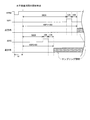
- FIG. 4 is a timing chart for explaining signals input to a timing controller in the first embodiment.
- 5 is a timing chart for explaining generation of a source start pulse signal in the first embodiment. In the said 1st Embodiment, it is a timing chart for demonstrating the signal input into the source driver when the shift direction is a forward direction.
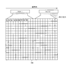
- FIG. 6 is a diagram illustrating a display order of display data to a pixel capacitor when the shift direction is a forward direction in the first embodiment.
- 5 is a timing chart for explaining signals input to the source driver when the shift direction is the reverse direction in the first embodiment.
- FIG. 6 is a diagram illustrating a writing order of display data to a pixel capacitor when the shift direction is the reverse direction in the first embodiment.
- FIG. 6 is a block diagram illustrating a configuration of a main part related to generation of a source start pulse signal in a liquid crystal display device according to a second embodiment of the present invention.
- 10 is a timing chart for explaining generation of a source start pulse signal in the second embodiment. It is a timing chart for demonstrating the effect in the said 2nd Embodiment. It is a block diagram which shows schematic structure of the gate driver in the 3rd Embodiment of this invention.
- FIG. 2 is a block diagram showing the overall configuration of the liquid crystal display device according to the first embodiment of the present invention.
- the liquid crystal display device includes a display unit 100, a timing controller 200, an EEPROM (electrically erasable read-only memory) 250, a source driver 300, and a gate driver 400.
- the EEPROM 250 is a nonvolatile memory.
- the source driver 300 includes two semiconductor chips (source driving IC chips SD1 and SD2).
- the gate driver 400 is composed of two semiconductor chips (gate driving IC chips GD1, GD2). Note that the number of semiconductor chips constituting the source driver 300 and the gate driver 400 is not limited to this.
- the liquid crystal display device will be described as adopting an SVGA type liquid crystal panel.
- the display unit 100 includes 1800 source bus lines (video signal lines) SL, 800 gate bus lines (scanning signal lines) GL, and intersections between the source bus lines and the gate bus lines. And a plurality of pixel forming portions provided. The plurality of pixel forming portions are arranged in a matrix to form a pixel array. Each pixel forming portion includes a TFT 10 that is a switching element having a gate terminal connected to a gate bus line GL that passes through a corresponding intersection and a source terminal connected to a source bus line SL that passes through the intersection.
- the liquid crystal capacitor 12 and the auxiliary capacitor 13 constitute a pixel capacitor. Note that only the components corresponding to one pixel formation portion are shown in the display portion 100 of FIG.
- One pixel forming portion forms one sub-pixel, and so-called one pixel is constituted by three sub-pixels of R (red), G (green), and B (blue).
- each sub-pixel has a long shape (vertically long shape) in the direction in which the source bus line extends, and sub-pixels of the same color continue in the direction in which the source bus line extends. It is the composition arranged.
- the timing controller 200 receives the image data DAT, a synchronization signal (horizontal synchronization signal HSYNC, vertical synchronization signal VSYNC, and clock CLK) and a horizontal shift direction instruction signal HSFT.
- the horizontal shift direction instruction signal HSFT is a signal for instructing a data shift direction in a shift register provided in the source driver 300.
- the timing controller 200 generates a source shift clock SCK, a digital video signal DV, and a latch strobe signal LS based on the image data DAT, the horizontal synchronization signal HSYNC, and the clock CLK, and outputs them.
- the timing controller 200 also receives a source start pulse signal (first source start pulse signal SSP1 or second source start pulse signal SSP2) based on the horizontal synchronization signal HSYNC, the clock CLK, and the horizontal shift direction instruction signal HSFT. Generate and output it.
- a first shift operation start instruction signal is realized by the first source start pulse signal SSP1
- a second shift operation start instruction signal is realized by the second source start pulse signal SSP2.
- the timing controller 200 further generates a gate start pulse signal GSP, a gate shift clock GCK, and a gate output enable signal GOE based on the vertical synchronization signal VSYNC and the clock CLK, and outputs them. Note that immediately after the liquid crystal display device is turned on, data stored in the EEPROM 250 is read out to a register 22 (see FIG. 1) described later in the timing controller 200.
- the source driver 300 includes a source start pulse signal (first source start pulse signal SSP1 or second source start pulse signal SSP2), a source shift clock SCK, a digital video signal DV, and a latch strobe signal output from the timing controller 200.
- LS is received, and a drive video signal is applied to each source bus line SL in order to charge the pixel capacitance of each pixel formation unit in the display unit 100.
- the gate driver 400 receives the gate start pulse signal GSP, the gate shift clock GCK, and the gate output enable signal GOE output from the timing controller 200, and sequentially applies active scanning signals to the gate bus lines GL in the display unit 100. To do.
- a driving video signal is applied to each source bus line SL, and a scanning signal is applied to each gate bus line GL, whereby an image based on image data DAT sent from the outside is displayed on the display unit 100. Is displayed.
- the source driver 300 includes a source driving IC chip SD1 and a source driving IC chip SD2.
- Each source driving IC chip is provided with 960 output terminals.
- all output terminals are connected to the source bus line SL in the display unit 100.
- the source driving IC chip SD2 840 output terminals are connected to the source bus line SL in the display unit 100, but the remaining 120 output terminals are connected to the source bus line SL in the display unit 100. Not connected. That is, in the source driving IC chip SD2, 120 extra outputs are generated.
- FIG. 4 is a block diagram showing a functional configuration of the source driver 300.
- a selection circuit 34 a buffer circuit 35 that applies the voltage selected by the selection circuit 34 to the source bus line SL as a driving video signal, and a level (grayscale voltage group) Vk corresponding to each grayscale level. And a regulated voltage generating circuit 36.
- These components are physically divided into a part included in the source driving IC chip SD1 and a part included in the source driving IC chip SD2. Further, as described above, with respect to the source driving IC chip SD2, the 120 output terminals located on the right side in FIGS. 2 and 4 are not connected to the source bus line SL in the display unit 100.
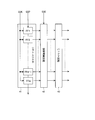
- the shift register 31 receives a source start pulse signal (first source start pulse signal SSP1 or second source start pulse signal SSP2) and a source shift clock SCK. Note that when the data shift direction in the shift register 31 is set to the forward direction (direction from FF1 to FFn), the first source start pulse signal SSP1 is input to the first-stage flip-flop FF1 of the shift register 31, and the shift is performed. When the direction is reversed (the direction from FFn to FF1), the second source start pulse signal SSP2 is input to the nth flip-flop FFn of the shift register 31.
- the shift register 31 sequentially transfers pulses included in the source start pulse signal from the input end to the output end based on the source shift clock SCK. In response to this pulse transfer, sampling pulses corresponding to the source bus lines SL are sequentially output from the shift register 31, and the sampling pulses are sequentially input to the sampling circuit 32.
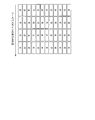
- the sampling circuit 32 samples the digital video signal DV sent from the timing controller 200 at the timing of the sampling pulse outputted from the shift register 31, and outputs it as an internal image signal d. More specifically, as shown in FIG. 5, the sampling circuit 32 includes a digital video signal DV (R) for R (red), a digital video signal DV (G) for G (green), and a digital video signal DV (G) for B (blue).
- the digital video signal DV (B) is input by separate signal lines, and they are sampled all at once by one sampling pulse. Then, internal image signals d for R (red), G (green), and B (blue) are output from the sampling circuit 32, respectively.
- the latch circuit 33 takes in the internal image signal d output from the sampling circuit 32 at the pulse timing of the latch strobe signal LS and outputs it.
- the gradation voltage generation circuit 36 generates a voltage corresponding to each gradation level based on a plurality of reference voltages supplied from a predetermined power supply circuit, and outputs these as a gradation voltage group Vk.
- the selection circuit 34 selects one of the gradation voltage groups Vk output from the gradation voltage generation circuit 36 based on the internal image signal d output from the latch circuit 33, and outputs the selected voltage. .
- the buffer circuit 35 performs impedance conversion of the voltage output from the selection circuit 34 using, for example, a voltage follower, and outputs the converted voltage to the source bus line SL as a driving video signal.
- the output from 120 output terminals (output terminals not connected to the source bus line SL) for the source driving IC chip SD2 is a dummy output.
- the gate driver 400 includes a gate driving IC chip GD1 and a gate driving IC chip GD2. Each gate driving IC chip is provided with 400 output terminals. In the present embodiment, all the output terminals of the gate driving IC chip GD1 and the gate driving IC chip GD2 are connected to the gate bus line GL in the display unit 100.
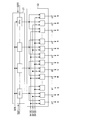
- FIG. 6 is a block diagram showing a functional configuration of the gate driver 400.
- a gate start pulse signal GSP and a gate shift clock GCK are input to the shift register 41.
- the shift register 41 Based on the gate shift clock GCK, the shift register 41 sequentially transfers pulses included in the gate start pulse signal from the input end to the output end, and sequentially outputs pulses from each stage to the logic operation circuit 42.
- the logical operation circuit 42 performs a logical operation between the pulse output from each stage of the shift register 41 and the gate output enable signal GOE.
- the output signal from the logical operation circuit 42 is level-converted by the buffer circuit 43 and applied to each gate bus line GL as a scanning signal.
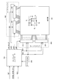
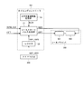
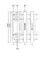
- FIG. 1 is a block diagram showing a configuration of a main part related to generation of a source start pulse signal.
- the timing controller 200 includes a source start pulse generation unit 21 and a register 22 as components for generating a source start pulse signal.
- a timing signal generation unit is realized by the timing controller 200, and a shift operation start instruction signal generation unit is realized by the source start pulse generation unit 21.
- the EEPROM 250 stores data indicating the length of a period (horizontal back porch) from the start of each horizontal scanning period to the time when shift (transfer) of data (here, the source start pulse signal) should start in the shift register 31. (Hereinafter referred to as “horizontal shift start setting data”) is stored in advance. Specifically, the horizontal shift start setting data when the shift direction of the shift register 31 is set to the forward direction is stored in the EEPROM 250 as the horizontal shift start setting data HSP1 for the forward direction, and the shift direction of the shift register 31 is set to the reverse direction. The horizontal shift start setting data is stored in the EEPROM 250 as the reverse horizontal shift start setting data HSP2.
- the first period length data is realized by the forward horizontal shift start setting data HSP1
- the second period length data is realized by the backward horizontal shift start setting data HSP2.
- the number of clocks is typically adopted as the horizontal shift start setting data, and the following description will be made on the assumption thereof.
- the register 22 is configured to store forward horizontal shift start setting data HSP1 and reverse horizontal shift start setting data HSP2.
- the forward horizontal shift start setting data HSP1 and the reverse horizontal shift start setting data HSP2 stored in advance in the EEPROM 250 are read to the register 22.
- the horizontal shift direction instruction signal HSFT is a digital signal.
- the horizontal shift direction instruction signal HSFT is set to a low level, and the shift direction of the shift register 31 is changed to the shift direction. In the reverse direction, it is assumed that the horizontal shift direction instruction signal HSFT is set to the high level.
- the source start pulse generator 21 generates a source start pulse signal (first source start pulse signal SSP1 or second source start pulse signal SSP2) based on the horizontal synchronization signal HSYNC, the clock CLK, and the horizontal shift direction instruction signal HSFT. Is generated. Specifically, if the horizontal shift direction instruction signal HSFT is at a low level, the source start pulse generator 21 refers to the forward horizontal shift start setting data HSP1 in the register 22 and refers to the horizontal synchronization signal HSYNC and the clock CLK. The first source start pulse signal SSP1 is generated based on the above.
- the source start pulse generation unit 21 refers to the horizontal shift start setting data HSP2 for reverse direction in the register 22 to generate the horizontal synchronization signal HSYNC and the clock CLK. Based on this, the second source start pulse signal SSP2 is generated.
- the shift start instruction signal receiving step is realized by the operation in which the source start pulse generator 21 receives the horizontal shift direction instruction signal HSFT, and the source start pulse generator 21 generates the source start pulse signal.
- the shift operation start instruction signal generation step is realized.
- the timing controller 200 displays display data for actual display on the display unit 100 as image data after 100 clocks have elapsed since the horizontal synchronization signal HSYNC changed from a high level to a low level. Input as DAT.
- the image data DAT consists of R data, G data, and B data, and these three data are input through separate signal lines.
- a delay occurs due to internal processing from the input of the image data DAT to the output of the digital video signal DV corresponding thereto.
- the delay time for this internal processing is defined as Td, and the time after Td has elapsed from the time when the horizontal synchronization signal HSYNC changes from high level to low level is defined as the start time of the horizontal scanning period as a unit period. Note that the method of determining the start time of the unit period is not limited to this.
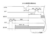
- FIG. 8 is a timing chart for explaining generation of the source start pulse signal. It is assumed that the value of the forward horizontal shift start setting data HSP1 is set to “100” and the value of the backward horizontal shift start setting data HSP2 is set to “60”. Further, it is assumed that three display data are input to the source driver 300 in a period corresponding to one clock.
- the horizontal shift direction instruction signal HSFT is at a low level
- data sampling within the source driver 300 (sampling of the digital video signal DV by the sampling circuit 32) is started after 100 clocks have elapsed from the start of the horizontal scanning period.
- the first source start pulse signal SSP1 is generated.
- the RSDS transmission method is adopted as the transmission method between the timing controller 200 and the source driver 300, as shown in FIG. 8, the first timing is reached after 98 clocks have elapsed since the start of the horizontal scanning period.
- the pulse of the source start pulse signal SSP1 rises. As shown in FIG.
- display data is input to the source driver 300 after 100 clocks have elapsed from the start of the horizontal scanning period, and sampling in the sampling circuit 32 is started in accordance with the display data input start timing.
- the display data sequentially input to the source driver 300 after 100 clocks have elapsed from the start of the horizontal scanning period is written into the pixel capacitance so as to be sequentially from the left side of the display unit 100 as shown in FIG. It is.
- an image formed as a result of writing to the pixel capacitor is displayed on the display unit 100 line by line.
- the second source start pulse signal SSP2 is generated so that sampling of data in the source driver 300 is started after 60 clocks have elapsed from the start of the horizontal scanning period. Is done.
- the second timing is reached after 58 clocks have elapsed since the start of the horizontal scanning period.
- the pulse of the source start pulse signal SSP2 rises.
- the display data is input to the source driver 300 after 100 clocks have elapsed since the start of the horizontal scanning period.
- the display data is displayed.
- Sampling by the sampling circuit 32 is started at a timing 40 clocks earlier than the input start timing. During the period of 40 clocks, sampling is performed on the line corresponding to the remainder output.
- the display data sequentially input to the source driver 300 after 100 clocks have elapsed from the start of the horizontal scanning period is written into the pixel capacitance so as to be sequentially from the right side of the display unit 100 as shown in FIG. It is. Then, an image formed as a result of writing to the pixel capacitor is displayed on the display unit 100 line by line.
- FIG. 1 1800 pieces of display data are input to the source driver 300 as a digital video signal DV per horizontal scanning period.
- the shift direction of the shift register 31 is the forward direction
- sampling of data in the source driver 300 is started in accordance with the timing at which display data input to the source driver 300 is started. Since the first to 600th stages of the shift register 31 are connected to the source bus line SL in the display unit 100, an image based on the display data is correctly displayed on the display unit 100.
- the shift direction of the shift register 31 is the reverse direction, sampling of data in the source driver 300 is performed at a timing earlier than the forward direction by a period corresponding to a period during which 120 display data are sent.
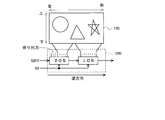
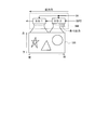
- FIG. 14 By the way, assuming that the shift direction is forward when the panel (display unit 100) and the source driver 300 (source driving IC chips SD1, SD2) are in the positional relationship as shown in FIG. 14, FIG. As shown, the shift direction is reversed when the installation position of the source driver 300 is reversed upside down from FIG. 14 or when an image reversed right and left from FIG. 14 is displayed as shown in FIG. . In FIG. 15, the letters “SD1” and “SD2” are displayed upside down in order to clarify the positional relationship between the output terminals of the source driving IC chips SD1 and SD2 and the display unit 100.
- the data sent from the timing controller 200 to the source driver 300 as the digital video signal DV is the shift direction.
- the order of the data may be the same between the forward direction and the backward direction. Therefore, processing for rearranging the order of data in the timing controller 200 is not necessary.
- the timing at which the display data is supplied to the source driver 300 as the digital video signal DV may be the same when the shift direction is the forward direction and the reverse direction. That is, a process of changing the timing of outputting display data from the timing controller 200 according to the shift direction (for example, a process of delaying) becomes unnecessary.
- FIG. 17 is a block diagram illustrating a configuration of a main part related to the generation of the source start pulse signal in the present embodiment.
- the timing controller 201 is provided with a horizontal scanning period length storage unit 23.
- the horizontal scanning period length storage unit 23 stores data indicating the length of one horizontal scanning period (hereinafter referred to as “horizontal scanning period length data”) HLEN. Note that the number of clocks is typically used as the horizontal scanning period length data, and the following description will be made on the assumption of this.
- a unit period length storage unit is realized by the horizontal scanning period length storage unit 23, and unit period length data is realized by the horizontal scanning period length data HLEN.
- the source start pulse generator 21 If the horizontal shift start setting data is set to a negative value, the source start pulse generator 21 generates the horizontal shift start setting data in the register 22 and the horizontal scanning period length data HLEN in the horizontal scanning period length storage unit 23.
- the source start pulse signal is generated based on the horizontal synchronization signal HSYNC and the clock CLK.
- the horizontal shift start setting data when the horizontal shift start setting data is set to a negative value, it is necessary to raise the pulse of the source start pulse signal at a timing earlier than the start time of each horizontal scanning period, but the horizontal scanning period length data HLEN By adding the horizontal shift start setting data, it is possible to determine how many clocks should elapse after the start of each horizontal scanning period before data sampling in the source driver 300 is started.
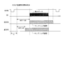
- FIG. 18 is a timing chart for explaining generation of the source start pulse signal.
- the value of the forward horizontal shift start setting data HSP1 is set to “10” and the value of the reverse horizontal shift start setting data HSP2 is set to “ ⁇ 30”.
- the horizontal shift direction instruction signal HSFT is at a low level
- the first source start pulse signal SSP1 is generated so that sampling of data in the source driver 300 is started after 10 clocks have elapsed from the start of the horizontal scanning period. Is done.
- the first timing is the timing after the elapse of 8 clocks from the start of the horizontal scanning period.
- the pulse of the source start pulse signal SSP1 rises. If the horizontal shift direction instruction signal HSFT is at a high level, the second source start pulse signal is set so that the sampling of data in the source driver 300 is started at a timing 30 clocks earlier than the start time of the horizontal scanning period. SSP2 is generated. For example, when the RSDS transmission method is adopted as the transmission method between the timing controller 201 and the source driver 300, as shown in FIG. 18, the second timing is 32 clocks earlier than the start time of the horizontal scanning period. The pulse of the source start pulse signal SSP2 rises.
- the bidirectional shift register is adopted as the shift register in the source driver.
- the bidirectional shift register is adopted as the shift register in the gate driver. . Note that it is assumed that a liquid crystal panel is an atypical panel and the number of pixels in the extending direction of the source bus line SL is 760.
- the gate driver 401 in the present embodiment is configured by two semiconductor chips (gate driving IC chips GD1, GD2). Each gate driving IC chip is provided with 400 output terminals. As for the gate driving IC chip GD1, all output terminals are connected to the gate bus line GL in the display unit 100. As for the gate driving IC chip GD2, as shown in FIG. 20, 360 output terminals are connected to the gate bus line GL in the display unit 100, but the remaining 40 output terminals are in the display unit 100. It is not connected to the gate bus line GL. In other words, in the gate driving IC chip GD2, 40 surplus outputs are generated.
- FIG. 21 is a block diagram showing a functional configuration of the gate driver 401 in the present embodiment.
- the shift register 41 has the first gate start pulse signal GSP1 or the second gate start as the gate start pulse signal.
- One of the pulse signals GSP2 is input.
- the first gate start pulse signal GSP1 is input to the first-stage flip-flop FF1 of the shift register 41, and the shift is performed.
- the second gate start pulse signal GSP2 is input to the m-th flip-flop FFm of the shift register 41.
- FIG. 22 is a block diagram showing a configuration of a main part related to generation of the gate start pulse signal.
- the timing controller 202 includes a gate start pulse generator 25 and a register 26 as components for generating a gate start pulse signal.
- a shift operation start instruction signal generation unit is realized by the gate start pulse generation unit 25.
- the vertical shift direction instruction signal VSFT is input to the timing controller 202 in place of the horizontal shift direction instruction signal HSFT in the first embodiment.
- the EEPROM 251 data indicating the length of a period (vertical back porch) from the start of each vertical scanning period to the time when shift (transfer) of data (here, the gate start pulse signal) is to be started in the shift register 41. (Hereinafter referred to as “vertical shift start setting data”) is stored in advance. Specifically, the vertical shift start setting data when the shift direction of the shift register 41 is set to the forward direction is stored in the EEPROM 251 as the vertical shift start setting data VSP1 for the forward direction, and the shift direction of the shift register 41 is set to the reverse direction.
- the vertical shift start setting data is stored in the EEPROM 251 as the reverse direction vertical shift start setting data VSP2.
- the first period length data is realized by the forward direction vertical shift start setting data VSP1
- the second period length data is realized by the reverse direction vertical shift start setting data VSP2. Note that the number of clocks is typically used as the vertical shift start setting data, and the following description will be made on the assumption of this.
- the register 26 is configured to store the vertical shift start setting data VSP1 for the forward direction and the vertical shift start setting data VSP2 for the reverse direction.
- forward vertical shift start setting data VSP1 and reverse vertical shift start setting data VSP2 stored in advance in the EEPROM 251 are read into the register 26.
- the vertical shift direction instruction signal VSFT is a digital signal, and when the shift direction of the shift register 41 is set to the forward direction, the vertical shift direction instruction signal VSFT is set to the low level, and the shift direction of the shift register 41 is changed to the shift direction. In the reverse direction, it is assumed that the vertical shift direction instruction signal VSFT is set to the high level.
- the gate start pulse generator 25 generates a gate start pulse signal (first gate start pulse signal GSP1 or second gate start pulse signal GSP2) based on the vertical synchronization signal VSYNC, the clock CLK, and the vertical shift direction instruction signal VSFT. Is generated. Specifically, if the vertical shift direction instruction signal VSFT is at a low level, the gate start pulse generating unit 25 refers to the vertical direction shift start setting data VSP1 for the forward direction in the register 26, and the vertical synchronization signal VSYNC and the clock CLK Based on this, the first gate start pulse signal GSP1 is generated.
- the gate start pulse generation unit 25 refers to the reverse direction vertical shift start setting data VSP2 in the register 26 to generate the vertical synchronization signal VSYNC and the clock CLK. Based on this, the second gate start pulse signal GSP2 is generated.
- the first shift operation start instruction signal is realized by the first gate start pulse signal GSP1
- the second shift operation start instruction signal is realized by the second gate start pulse signal GSP2. Yes.
- 800 pulses per vertical scanning period are output from the shift register 41 to the logic operation circuit 42 in the gate driver 401.
- the vertical shift start setting data VSP1 for the forward direction and the vertical shift start setting data VSP2 for the reverse direction are set to appropriate values, even if the shift direction of the shift register 41 is the forward direction, the reverse direction is reversed.
- active scanning is sequentially performed on each gate bus line GL in the display unit 100 during a period in which a driving video signal corresponding to an image of one frame (one screen) is output from the source driver 300. A signal is applied.
- the gate driver 401 produces a surplus output, the same image as when the shift direction is the forward direction can be displayed even if the shift direction of the shift register 41 is reversed.
- the gate start pulse signal is generated based on data indicating the length of one vertical scanning period and vertical shift start setting data set to a negative value.
- the length of one vertical scanning period can be shortened.
- the liquid crystal display device has been described as an example, but the present invention is not limited to this.
- the present invention can also be applied to other display devices such as organic EL (Electro Luminescence).
- each sub-pixel has a long shape (vertically long shape) in the direction in which the source bus line extends, and the sub-pixels of the same color Are arranged continuously in the direction in which the source bus line extends, and as shown in FIG. 23, each sub-pixel has a long shape (horizontal shape) in the direction in which the gate bus line extends, and the same color.
- the sub-pixels are continuously arranged in the extending direction of the gate bus line.
- three display data are sampled by one sampling pulse in the source driver.
- one display data is sampled by one sampling pulse in the source driver.
- one gate bus line is selected in one horizontal scanning period.
- the number of gate bus lines is three times that in the configuration shown in FIG. 3, so that one gate bus line is selected in one-third horizontal scanning period. . That is, in the case of the configuration shown in FIG. 23, the scanning speed of the gate bus line is three times that of the configuration shown in FIG.
- the description has been made on the assumption that the pixel configuration is the configuration shown in FIG. 3, but the present invention can also be applied to a liquid crystal display device having the pixel configuration shown in FIG. .
- a so-called “one-chip driver” in which a timing controller, a source driver, a gate driver, and the like are integrated in one semiconductor chip is sometimes used as a driving IC for a liquid crystal panel (see FIG. 24).
- Such a one-chip driver is provided with a large number of output terminals for connection to source bus lines and gate bus lines. By the way, even in a one-chip driver, a surplus output may be generated in the source driver or the gate driver. Also, the shift direction of the shift register should be reversed in the source driver and gate driver in the one-chip driver.
- the shift register is operated by operating the source driver in the same manner as in the first embodiment or the second embodiment. It is possible to perform the same image display when the shift direction is forward and reverse. Also, if there is a surplus output in the gate driver, the gate driver is operated in the same manner as in the third embodiment, so that the shift register is operated in the forward direction and in the reverse direction. It is possible to perform image display.
- Reverse-direction vertical shift start setting data HLEN ... Horizontal scanning period length data HSFT ... Horizontal shift direction instruction signal VSFT ... Vertical shift direction instruction signal SSP1 ... first source start pulse signal SSP2 ; second source start pulse signal GSP1 ... first gate start pulse signal GSP2 ; second gate start pulse signal
Landscapes
- Engineering & Computer Science (AREA)
- Chemical & Material Sciences (AREA)
- Crystallography & Structural Chemistry (AREA)
- Physics & Mathematics (AREA)
- Computer Hardware Design (AREA)
- General Physics & Mathematics (AREA)
- Theoretical Computer Science (AREA)
- Control Of Indicators Other Than Cathode Ray Tubes (AREA)
- Liquid Crystal Display Device Control (AREA)
Abstract
Description
前記双方向シフトレジスタのシフト方向が第1の方向になっているときにおける、単位期間の開始時点から前記双方向シフトレジスタのシフト動作が開始されるべき時点までの期間の長さを示す第1の期間長データと、前記双方向シフトレジスタのシフト方向が前記第1の方向とは逆方向である第2の方向になっているときにおける、単位期間の開始時点から前記双方向シフトレジスタのシフト動作が開始されるべき時点までの期間の長さを示す第2の期間長データとを格納するレジスタ部と、
各単位期間における前記双方向シフトレジスタのシフト動作の開始タイミングを示す信号として、前記双方向シフトレジスタのシフト方向が前記第1の方向となるように前記信号線駆動部を動作させる第1のシフト動作開始指示信号と、前記双方向シフトレジスタのシフト方向が前記第2の方向となるように前記信号線駆動部を動作させる第2のシフト動作開始指示信号とを生成するためのシフト動作開始指示信号生成部と
を備え、
前記シフト動作開始指示信号生成部は、前記双方向シフトレジスタのシフト方向を示すシフト方向指示信号を受け取り、前記シフト方向指示信号が前記第1の方向を示しているときには、前記第1の期間長データに基づき前記第1のシフト動作開始指示信号を生成し、前記シフト方向指示信号が前記第2の方向を示しているときには、前記第2の期間長データに基づき前記第2のシフト動作開始指示信号を生成することを特徴とする。
前記第1の期間長データおよび前記第2の期間長データを格納するための不揮発性メモリを更に備え、
前記第1の期間長データおよび前記第2の期間長データは、電源投入後に、前記不揮発性メモリから前記レジスタ部に読み出されることを特徴とする。
前記単位期間の長さを示す単位期間長データを格納する単位期間長記憶部を更に備え、
前記レジスタ部は、前記第1の期間長データおよび前記第2の期間長データの少なくとも一方について負の値を格納することができるように構成され、
前記シフト動作開始指示信号生成部は、前記シフト方向指示信号が前記第1の方向を示しているとき、前記第1の期間長データが負の値であれば、前記単位期間長データと前記第1の期間長データとに基づき前記第1のシフト動作開始指示信号を生成し、前記シフト方向指示信号が前記第2の方向を示しているとき、前記第2の期間長データが負の値であれば、前記単位期間長データと前記第2の期間長データとに基づき前記第2のシフト動作開始指示信号を生成することを特徴とする。
前記表示部には、前記複数の信号線として複数の映像信号線が配設され、
前記信号線駆動部は、前記複数の映像信号線を駆動する映像信号線駆動部であることを特徴とする。
前記表示部には、前記複数の信号線として複数の走査信号線が配設され、
前記信号線駆動部は、前記複数の走査信号線を駆動する走査信号線駆動部であることを特徴とする。
前記表示部には、前記複数の信号線として複数の映像信号線と複数の走査信号線とが配設され、
前記信号線駆動部は、前記複数の映像信号線を駆動する映像信号線駆動部と前記複数の走査信号線を駆動する走査信号線駆動部とからなることを特徴とする。
前記レジスタ部および前記シフト動作開始指示信号生成部を含み、前記映像信号線駆動部および前記走査信号線駆動部の動作を制御するためのタイミング信号を生成するタイミング信号生成部を更に備え、
前記映像信号線駆動部,前記走査信号線駆動部,および前記タイミング信号生成部のうちのいずれか2つ以上が1つの半導体チップの中に形成されていることを特徴とする。
前記信号線駆動部は、前記複数の信号線のいずれにも接続されていない出力端子であるダミー端子を有する半導体チップを含む1以上の半導体チップによって構成され、
前記複数の出力段のうち前記ダミー端子に対応する出力段において前記双方向シフトレジスタのシフト動作が行われる期間の長さを示すデータが前記第1の期間長データまたは前記第2の期間長データとして前記レジスタ部に格納されていることを特徴とする。
前記双方向シフトレジスタのシフト方向を示すシフト方向指示信号を受け取るシフト方向指示信号受信ステップと、
各単位期間における前記双方向シフトレジスタのシフト動作の開始タイミングを示す信号として、前記双方向シフトレジスタのシフト方向が第1の方向となるように前記信号線駆動部を動作させる第1のシフト動作開始指示信号または前記双方向シフトレジスタのシフト方向が前記第1の方向とは逆方向である第2の方向となるように前記信号線駆動部を動作させる第2のシフト動作開始指示信号を生成するシフト動作開始指示信号生成ステップと
を含み、
前記表示装置は、前記双方向シフトレジスタのシフト方向が前記第1の方向になっているときにおける、単位期間の開始時点から前記双方向シフトレジスタのシフト動作が開始されるべき時点までの期間の長さを示す第1の期間長データと、前記双方向シフトレジスタのシフト方向が前記第2の方向になっているときにおける、単位期間の開始時点から前記双方向シフトレジスタのシフト動作が開始されるべき時点までの期間の長さを示す第2の期間長データとを格納するレジスタ部を更に備え、
前記シフト動作開始指示信号生成ステップでは、前記シフト方向指示信号が前記第1の方向を示しているときには、前記第1の期間長データに基づき前記第1のシフト動作開始指示信号が生成され、前記シフト方向指示信号が前記第2の方向を示しているときには、前記第2の期間長データに基づき前記第2のシフト動作開始指示信号が生成されることを特徴とする。
<1.1 全体構成>
図2は、本発明の第1の実施形態に係る液晶表示装置の全体構成を示すブロック図である。この液晶表示装置は、表示部100とタイミングコントローラ200とEEPROM(電気的に消去可能な読み出し専用メモリ)250とソースドライバ300とゲートドライバ400とを備えている。EEPROM250は、不揮発性メモリである。ソースドライバ300は、2つの半導体チップ(ソース駆動用ICチップSD1,SD2)によって構成されている。ゲートドライバ400は、2つの半導体チップ(ゲート駆動用ICチップGD1,GD2)によって構成されている。なお、ソースドライバ300やゲートドライバ400を構成する半導体チップの個数については、これに限定されない。以下、この液晶表示装置はSVGA型の液晶パネルを採用しているものとして説明する。
次に、駆動部(ソースドライバ300およびゲートドライバ400)の詳細な構成について説明する。なお、以下に示す構成は一例であって、それ以外の構成にも本発明を適用することができる。
図2に示すように、ソースドライバ300は、ソース駆動用ICチップSD1とソース駆動用ICチップSD2とによって構成されている。各ソース駆動用ICチップには960個の出力端子が設けられている。ソース駆動用ICチップSD1については、全ての出力端子が表示部100内のソースバスラインSLに接続されている。ソース駆動用ICチップSD2については、840個の出力端子は表示部100内のソースバスラインSLに接続されているが、残りの120個の出力端子は表示部100内のソースバスラインSLには接続されていない。すなわち、ソース駆動用ICチップSD2においては、120個の余り出力が生じる。
図2に示すように、ゲートドライバ400は、ゲート駆動用ICチップGD1とゲート駆動用ICチップGD2とによって構成されている。各ゲート駆動用ICチップには400個の出力端子が設けられている。本実施形態においては、ゲート駆動用ICチップGD1についても、ゲート駆動用ICチップGD2についても、全ての出力端子が表示部100内のゲートバスラインGLに接続されている。
図1は、ソーススタートパルス信号の生成に関わる要部の構成を示すブロック図である。タイミングコントローラ200は、ソーススタートパルス信号を生成するための構成要素として、ソーススタートパルス生成部21とレジスタ22とを備えている。なお、本実施形態においては、タイミングコントローラ200によってタイミング信号生成部が実現され、ソーススタートパルス生成部21によってシフト動作開始指示信号生成部が実現されている。
図13を参照しつつ、本実施形態における効果について説明する。本実施形態においては、1水平走査期間につき1800個の表示データがデジタル映像信号DVとしてソースドライバ300に入力される。ここで、シフトレジスタ31のシフト方向が順方向のときには、ソースドライバ300への表示データの入力が開始されるタイミングに合わせて、ソースドライバ300内でのデータのサンプリングが開始される。シフトレジスタ31の1段目から600段目までは表示部100内のソースバスラインSLに接続されているので、表示データに基づく画像が正しく表示部100に表示される。一方、シフトレジスタ31のシフト方向が逆方向のときには、順方向のときに比べて120個の表示データが送られてくる期間に相当する期間だけ早いタイミングでソースドライバ300内でのデータのサンプリングが開始される。このため、ソース駆動用ICチップSD2において、ダミー出力用のライン(シフトレジスタ31の601段目から640段目に対応するライン)に表示データが取り込まれることはなく、シフトレジスタ31の600段目に対応するラインから正しく表示データのサンプリングが行われる。これにより、シフトレジスタ31のシフト方向が順方向のときと逆方向のときとで画像の表示位置にずれが生じることはない。また、シフトレジスタ31のシフト方向を逆方向にしたときに画像の欠落が生じることもない。以上のように、ソースドライバ300において余り出力が生じている場合にシフトレジスタ31のシフト方向が逆方向にされても、シフト方向が順方向のときと同様の画像を表示することが可能となる。
<2.1 構成など>
本実施形態においては、全体構成および駆動部の構成については上記第1の実施形態と同様であるので説明を省略する。図17は、本実施形態におけるソーススタートパルス信号の生成に関わる要部の構成を示すブロック図である。タイミングコントローラ201には、上記第1の実施形態における構成要素に加えて、水平走査期間長記憶部23が設けられている。この水平走査期間長記憶部23には、1水平走査期間の長さを示すデータ(以下、「水平走査期間長データ」という。)HLENが格納されている。なお、水平走査期間長データとしては典型的にはクロック数が採用され、以下においてもそれを前提に説明する。また、本実施形態においては、水平走査期間長記憶部23によって単位期間長記憶部が実現され、水平走査期間長データHLENによって単位期間長データが実現されている。
図19を参照しつつ、本実施形態における効果について説明する。本実施形態によれば、上記第1の実施形態と同様の効果が得られるほか、次のような効果が得られる。シフトレジスタ31のシフト方向が順方向のときには、上記第1の実施形態と同様、ソースドライバ300への表示データの入力が開始されるタイミングに合わせて、ソースドライバ300内でのデータのサンプリングが開始される。これにより、表示データに基づく画像が正しく表示部100に表示される。一方、シフトレジスタ31のシフト方向が逆方向のときには、水平走査期間の開始時点よりも30クロックだけ早いタイミングでソースドライバ300内でのデータのサンプリングが開始される。この30クロック分の期間および水平走査期間の開始時点から表示データのサンプリングが開始されるまでの10クロック分の期間(合計40クロック分の期間)には、ダミー出力用のラインにおけるデータのサンプリングが行われる。このとき、ダミー出力用のラインに表示データが取り込まれることはない。そして、ダミー出力用のラインにおけるデータのサンプリングの終了後、表示データのサンプリングが開始され、順方向のときと表示位置にずれが生じることなく画像が表示される。このように、水平シフト開始設定データの値を適宜の値に設定しておくことによって、ダミー出力用のラインにおけるデータのサンプリングを水平走査期間の開始前に行うことが可能となり、水平バックポーチが短縮される。これにより、1水平走査期間の長さの短縮,クロック周波数の低減,消費電流の低減が可能となる。
上記第1および第2の実施形態においてはソースドライバ内のシフトレジスタに双方向シフトレジスタが採用されていたが、本実施形態においてはゲートドライバ内のシフトレジスタに双方向シフトレジスタが採用されている。なお、液晶パネルには異型パネルが採用されていてソースバスラインSLの伸びる方向についての画素数が760個であると仮定する。
本実施形態におけるゲートドライバ401は、上記第1の実施形態と同様、2つの半導体チップ(ゲート駆動用ICチップGD1,GD2)によって構成されている。各ゲート駆動用ICチップには400個の出力端子が設けられている。ゲート駆動用ICチップGD1については、全ての出力端子が表示部100内のゲートバスラインGLに接続されている。ゲート駆動用ICチップGD2については、図20に示すように、360個の出力端子は表示部100内のゲートバスラインGLに接続されているが、残りの40個の出力端子は表示部100内のゲートバスラインGLには接続されていない。すなわち、ゲート駆動用ICチップGD2においては、40個の余り出力が生じる。
図22は、ゲートスタートパルス信号の生成に関わる要部の構成を示すブロック図である。本実施形態においては、タイミングコントローラ202は、ゲートスタートパルス信号を生成するための構成要素として、ゲートスタートパルス生成部25とレジスタ26とを備えている。なお、本実施形態においては、ゲートスタートパルス生成部25によってシフト動作開始指示信号生成部が実現されている。
本実施形態においては、ゲートドライバ401内で1垂直走査期間につき800個のパルスがシフトレジスタ41から論理演算回路42へと出力される。ここで、順方向用垂直シフト開始設定データVSP1および逆方向用垂直シフト開始設定データVSP2を適宜の値に設定しておくことによって、シフトレジスタ41のシフト方向が順方向であっても逆方向であっても、1フレーム分(1画面分)の画像に対応する駆動用映像信号がソースドライバ300から出力されている期間中に、表示部100内の各ゲートバスラインGLに順次にアクティブな走査信号が印加される。これにより、ゲートドライバ401において余り出力が生じている場合にシフトレジスタ41のシフト方向が逆方向にされても、シフト方向が順方向のときと同様の画像を表示することが可能となる。
上記各実施形態においては、ソースドライバまたはゲートドライバの一方において余り出力が生じている場合を例に挙げて説明した。しかしながら、本発明はこれに限定されず、ソースドライバおよびゲートドライバの双方において余り出力が生じている場合にも本発明を適用することができる。
22,26…レジスタ
25…ゲートスタートパルス生成部
31…(ソースドライバ内の)シフトレジスタ
32…サンプリング回路
41…(ゲートドライバ内の)シフトレジスタ
100…表示部
200,201,202…タイミングコントローラ
250,251…EEPROM
300…ソースドライバ
400,401…ゲートドライバ
SD1,SD2…ソース駆動用ICチップ
GD1,GD2…ゲート駆動用ICチップ
HSYNC…水平同期信号
VSYNC…垂直同期信号
HSP1…順方向用水平シフト開始設定データ
HSP2…逆方向用水平シフト開始設定データ
VSP1…順方向用垂直シフト開始設定データ
VSP2…逆方向用垂直シフト開始設定データ
HLEN…水平走査期間長データ
HSFT…水平シフト方向指示信号
VSFT…垂直シフト方向指示信号
SSP1…第1のソーススタートパルス信号
SSP2…第2のソーススタートパルス信号
GSP1…第1のゲートスタートパルス信号
GSP2…第2のゲートスタートパルス信号
Claims (9)
- 表示部と、前記表示部に配設された複数の信号線と、複数の出力段からなる双方向シフトレジスタを有し前記双方向シフトレジスタのシフト動作に伴い前記複数の出力段から順次に出力されるパルスに基づき前記複数の信号線を駆動する信号線駆動部とを備えた表示装置であって、
前記双方向シフトレジスタのシフト方向が第1の方向になっているときにおける、単位期間の開始時点から前記双方向シフトレジスタのシフト動作が開始されるべき時点までの期間の長さを示す第1の期間長データと、前記双方向シフトレジスタのシフト方向が前記第1の方向とは逆方向である第2の方向になっているときにおける、単位期間の開始時点から前記双方向シフトレジスタのシフト動作が開始されるべき時点までの期間の長さを示す第2の期間長データとを格納するレジスタ部と、
各単位期間における前記双方向シフトレジスタのシフト動作の開始タイミングを示す信号として、前記双方向シフトレジスタのシフト方向が前記第1の方向となるように前記信号線駆動部を動作させる第1のシフト動作開始指示信号と、前記双方向シフトレジスタのシフト方向が前記第2の方向となるように前記信号線駆動部を動作させる第2のシフト動作開始指示信号とを生成するためのシフト動作開始指示信号生成部と
を備え、
前記シフト動作開始指示信号生成部は、前記双方向シフトレジスタのシフト方向を示すシフト方向指示信号を受け取り、前記シフト方向指示信号が前記第1の方向を示しているときには、前記第1の期間長データに基づき前記第1のシフト動作開始指示信号を生成し、前記シフト方向指示信号が前記第2の方向を示しているときには、前記第2の期間長データに基づき前記第2のシフト動作開始指示信号を生成することを特徴とする、表示装置。 - 前記第1の期間長データおよび前記第2の期間長データを格納するための不揮発性メモリを更に備え、
前記第1の期間長データおよび前記第2の期間長データは、電源投入後に、前記不揮発性メモリから前記レジスタ部に読み出されることを特徴とする、請求項1に記載の表示装置。 - 前記単位期間の長さを示す単位期間長データを格納する単位期間長記憶部を更に備え、
前記レジスタ部は、前記第1の期間長データおよび前記第2の期間長データの少なくとも一方について負の値を格納することができるように構成され、
前記シフト動作開始指示信号生成部は、前記シフト方向指示信号が前記第1の方向を示しているとき、前記第1の期間長データが負の値であれば、前記単位期間長データと前記第1の期間長データとに基づき前記第1のシフト動作開始指示信号を生成し、前記シフト方向指示信号が前記第2の方向を示しているとき、前記第2の期間長データが負の値であれば、前記単位期間長データと前記第2の期間長データとに基づき前記第2のシフト動作開始指示信号を生成することを特徴とする、請求項1に記載の表示装置。 - 前記表示部には、前記複数の信号線として複数の映像信号線が配設され、
前記信号線駆動部は、前記複数の映像信号線を駆動する映像信号線駆動部であることを特徴とする、請求項1に記載の表示装置。 - 前記表示部には、前記複数の信号線として複数の走査信号線が配設され、
前記信号線駆動部は、前記複数の走査信号線を駆動する走査信号線駆動部であることを特徴とする、請求項1に記載の表示装置。 - 前記表示部には、前記複数の信号線として複数の映像信号線と複数の走査信号線とが配設され、
前記信号線駆動部は、前記複数の映像信号線を駆動する映像信号線駆動部と前記複数の走査信号線を駆動する走査信号線駆動部とからなることを特徴とする、請求項1に記載の表示装置。 - 前記レジスタ部および前記シフト動作開始指示信号生成部を含み、前記映像信号線駆動部および前記走査信号線駆動部の動作を制御するためのタイミング信号を生成するタイミング信号生成部を更に備え、
前記映像信号線駆動部,前記走査信号線駆動部,および前記タイミング信号生成部のうちのいずれか2つ以上が1つの半導体チップの中に形成されていることを特徴とする、請求項6に記載の表示装置。 - 前記信号線駆動部は、前記複数の信号線のいずれにも接続されていない出力端子であるダミー端子を有する半導体チップを含む1以上の半導体チップによって構成され、
前記複数の出力段のうち前記ダミー端子に対応する出力段において前記双方向シフトレジスタのシフト動作が行われる期間の長さを示すデータが前記第1の期間長データまたは前記第2の期間長データとして前記レジスタ部に格納されていることを特徴とする、請求項1に記載の表示装置。 - 表示部と、前記表示部に配設された複数の信号線と、複数の出力段からなる双方向シフトレジスタを有し前記双方向シフトレジスタのシフト動作に伴い前記複数の出力段から順次に出力されるパルスに基づき前記複数の信号線を駆動する信号線駆動部とを備えた表示装置の駆動方法であって、
前記双方向シフトレジスタのシフト方向を示すシフト方向指示信号を受け取るシフト方向指示信号受信ステップと、
各単位期間における前記双方向シフトレジスタのシフト動作の開始タイミングを示す信号として、前記双方向シフトレジスタのシフト方向が第1の方向となるように前記信号線駆動部を動作させる第1のシフト動作開始指示信号または前記双方向シフトレジスタのシフト方向が前記第1の方向とは逆方向である第2の方向となるように前記信号線駆動部を動作させる第2のシフト動作開始指示信号を生成するシフト動作開始指示信号生成ステップと
を含み、
前記表示装置は、前記双方向シフトレジスタのシフト方向が前記第1の方向になっているときにおける、単位期間の開始時点から前記双方向シフトレジスタのシフト動作が開始されるべき時点までの期間の長さを示す第1の期間長データと、前記双方向シフトレジスタのシフト方向が前記第2の方向になっているときにおける、単位期間の開始時点から前記双方向シフトレジスタのシフト動作が開始されるべき時点までの期間の長さを示す第2の期間長データとを格納するレジスタ部を更に備え、
前記シフト動作開始指示信号生成ステップでは、前記シフト方向指示信号が前記第1の方向を示しているときには、前記第1の期間長データに基づき前記第1のシフト動作開始指示信号が生成され、前記シフト方向指示信号が前記第2の方向を示しているときには、前記第2の期間長データに基づき前記第2のシフト動作開始指示信号が生成されることを特徴とする、駆動方法。
Priority Applications (2)
| Application Number | Priority Date | Filing Date | Title |
|---|---|---|---|
| CN201180050237.5A CN103155027B (zh) | 2010-10-21 | 2011-10-17 | 显示装置 |
| US13/877,921 US8922473B2 (en) | 2010-10-21 | 2011-10-17 | Display device with bidirectional shift register and method of driving same |
Applications Claiming Priority (2)
| Application Number | Priority Date | Filing Date | Title |
|---|---|---|---|
| JP2010-236294 | 2010-10-21 | ||
| JP2010236294 | 2010-10-21 |
Publications (1)
| Publication Number | Publication Date |
|---|---|
| WO2012053466A1 true WO2012053466A1 (ja) | 2012-04-26 |
Family
ID=45975178
Family Applications (1)
| Application Number | Title | Priority Date | Filing Date |
|---|---|---|---|
| PCT/JP2011/073797 Ceased WO2012053466A1 (ja) | 2010-10-21 | 2011-10-17 | 表示装置およびその駆動方法 |
Country Status (3)
| Country | Link |
|---|---|
| US (1) | US8922473B2 (ja) |
| CN (1) | CN103155027B (ja) |
| WO (1) | WO2012053466A1 (ja) |
Families Citing this family (8)
| Publication number | Priority date | Publication date | Assignee | Title |
|---|---|---|---|---|
| JP6286142B2 (ja) * | 2013-06-20 | 2018-02-28 | ラピスセミコンダクタ株式会社 | 表示装置、及びソースドライバ |
| KR102155015B1 (ko) * | 2014-09-29 | 2020-09-15 | 삼성전자주식회사 | 소스 드라이버 및 그것의 동작 방법 |
| CN105161068B (zh) * | 2015-10-19 | 2017-06-16 | 昆山龙腾光电有限公司 | 一种用于显示装置的驱动芯片和显示装置 |
| US20170221402A1 (en) * | 2016-01-29 | 2017-08-03 | Panasonic Liquid Crystal Display Co., Ltd. | Display device |
| KR102485563B1 (ko) * | 2016-02-02 | 2023-01-09 | 삼성디스플레이 주식회사 | 표시 패널 구동 장치, 이를 이용한 표시 패널 구동 방법 및 이를 포함하는 표시 장치 |
| JP2018063351A (ja) * | 2016-10-13 | 2018-04-19 | 株式会社ジャパンディスプレイ | 有機el表示装置及び有機el表示装置の駆動方法 |
| KR102753023B1 (ko) * | 2020-12-31 | 2025-01-09 | 엘지디스플레이 주식회사 | 표시장치 |
| CN113920911B (zh) * | 2021-06-25 | 2022-07-12 | 惠科股份有限公司 | 显示面板的驱动电路及方法、显示装置 |
Citations (3)
| Publication number | Priority date | Publication date | Assignee | Title |
|---|---|---|---|---|
| JPH05249927A (ja) * | 1992-03-09 | 1993-09-28 | Oki Lsi Tekunoroji Kansai:Kk | 駆動回路 |
| JPH1074062A (ja) * | 1996-08-30 | 1998-03-17 | Sanyo Electric Co Ltd | 双方向シフトレジスタ及び液晶表示装置 |
| JP2010139535A (ja) * | 2008-12-09 | 2010-06-24 | Seiko Epson Corp | 電気光学装置及び電子機器 |
Family Cites Families (8)
| Publication number | Priority date | Publication date | Assignee | Title |
|---|---|---|---|---|
| JP3167435B2 (ja) * | 1992-07-27 | 2001-05-21 | ローム株式会社 | ドライバー回路 |
| JP2002182614A (ja) * | 2000-12-11 | 2002-06-26 | Seiko Epson Corp | 半導体装置 |
| JP4679812B2 (ja) * | 2002-11-07 | 2011-05-11 | シャープ株式会社 | 走査方向制御回路および表示装置 |
| JP4044020B2 (ja) * | 2003-06-10 | 2008-02-06 | シャープ株式会社 | 双方向シフトレジスタ、および、それを備えた表示装置 |
| JP2005004120A (ja) | 2003-06-16 | 2005-01-06 | Advanced Display Inc | 表示装置及び表示制御回路 |
| JP4152934B2 (ja) * | 2003-11-25 | 2008-09-17 | シャープ株式会社 | 表示装置及びその駆動方法 |
| KR100598741B1 (ko) * | 2003-12-11 | 2006-07-10 | 엘지.필립스 엘시디 주식회사 | 액정표시장치 |
| KR101096712B1 (ko) * | 2004-12-28 | 2011-12-22 | 엘지디스플레이 주식회사 | 액정표시장치 및 이의 구동방법 |
-
2011
- 2011-10-17 CN CN201180050237.5A patent/CN103155027B/zh not_active Expired - Fee Related
- 2011-10-17 WO PCT/JP2011/073797 patent/WO2012053466A1/ja not_active Ceased
- 2011-10-17 US US13/877,921 patent/US8922473B2/en not_active Expired - Fee Related
Patent Citations (3)
| Publication number | Priority date | Publication date | Assignee | Title |
|---|---|---|---|---|
| JPH05249927A (ja) * | 1992-03-09 | 1993-09-28 | Oki Lsi Tekunoroji Kansai:Kk | 駆動回路 |
| JPH1074062A (ja) * | 1996-08-30 | 1998-03-17 | Sanyo Electric Co Ltd | 双方向シフトレジスタ及び液晶表示装置 |
| JP2010139535A (ja) * | 2008-12-09 | 2010-06-24 | Seiko Epson Corp | 電気光学装置及び電子機器 |
Also Published As
| Publication number | Publication date |
|---|---|
| CN103155027B (zh) | 2015-10-14 |
| US20130187843A1 (en) | 2013-07-25 |
| US8922473B2 (en) | 2014-12-30 |
| CN103155027A (zh) | 2013-06-12 |
Similar Documents
| Publication | Publication Date | Title |
|---|---|---|
| KR102001890B1 (ko) | 액정표시장치 | |
| KR101493276B1 (ko) | 타이밍 컨트롤러, 액정 표시 장치 및 액정 표시 장치의구동 방법 | |
| KR100883812B1 (ko) | 화상표시장치 | |
| CN101884062B (zh) | 显示装置及显示装置的驱动方法 | |
| KR101840186B1 (ko) | 액정 표시 장치 및 그 구동 방법 | |
| US8624812B2 (en) | Liquid crystal display | |
| WO2012053466A1 (ja) | 表示装置およびその駆動方法 | |
| KR101082909B1 (ko) | 게이트 구동 방법 및 그 장치와 이를 갖는 표시장치 | |
| US20060193002A1 (en) | Drive circuit chip and display device | |
| KR20060003968A (ko) | 어레이 기판과 이를 갖는 표시 장치와, 이의 구동장치 및방법 | |
| JP2011039205A (ja) | タイミングコントローラ、画像表示装置及びリセット信号出力方法 | |
| US11282466B2 (en) | Driver device | |
| KR20020067097A (ko) | 액정 표시 장치와 이의 구동 장치 및 방법 | |
| KR20190079855A (ko) | 시프트 레지스터 및 이를 포함하는 표시 장치 | |
| US20110157249A1 (en) | Reference voltage generating circuit and method for generating gamma reference voltage | |
| US8976208B2 (en) | Display apparatus and driving method thereof | |
| KR102135928B1 (ko) | 쉬프트 레지스터 및 그 제조방법, 그리고 쉬프트 레지스터를 이용한 영상 표시장치 | |
| KR101989931B1 (ko) | 액정표시장치 | |
| US8493311B2 (en) | Display device | |
| CN101162335A (zh) | 栅极驱动器、光电装置、电子设备以及驱动方法 | |
| CN1967646B (zh) | 液晶显示器的驱动装置 | |
| JP5239177B2 (ja) | 表示駆動装置及びそれを備えた表示装置 | |
| US7471278B2 (en) | Display driver, electro-optical device, and drive method | |
| JP3775188B2 (ja) | 液晶表示装置及びその液晶表示装置を備えた情報機器 | |
| KR20110078710A (ko) | 액정표시장치 |
Legal Events
| Date | Code | Title | Description |
|---|---|---|---|
| WWE | Wipo information: entry into national phase |
Ref document number: 201180050237.5 Country of ref document: CN |
|
| 121 | Ep: the epo has been informed by wipo that ep was designated in this application |
Ref document number: 11834305 Country of ref document: EP Kind code of ref document: A1 |
|
| WWE | Wipo information: entry into national phase |
Ref document number: 13877921 Country of ref document: US |
|
| NENP | Non-entry into the national phase |
Ref country code: DE |
|
| 122 | Ep: pct application non-entry in european phase |
Ref document number: 11834305 Country of ref document: EP Kind code of ref document: A1 |
|
| NENP | Non-entry into the national phase |
Ref country code: JP |