WO2012050122A1 - Soi基板 - Google Patents
Soi基板 Download PDFInfo
- Publication number
- WO2012050122A1 WO2012050122A1 PCT/JP2011/073412 JP2011073412W WO2012050122A1 WO 2012050122 A1 WO2012050122 A1 WO 2012050122A1 JP 2011073412 W JP2011073412 W JP 2011073412W WO 2012050122 A1 WO2012050122 A1 WO 2012050122A1
- Authority
- WO
- WIPO (PCT)
- Prior art keywords
- film
- soi substrate
- carbon film
- substrate
- silicon
- Prior art date
- Legal status (The legal status is an assumption and is not a legal conclusion. Google has not performed a legal analysis and makes no representation as to the accuracy of the status listed.)
- Ceased
Links
Images





Classifications
-
- H—ELECTRICITY
- H10—SEMICONDUCTOR DEVICES; ELECTRIC SOLID-STATE DEVICES NOT OTHERWISE PROVIDED FOR
- H10P—GENERIC PROCESSES OR APPARATUS FOR THE MANUFACTURE OR TREATMENT OF DEVICES COVERED BY CLASS H10
- H10P90/00—Preparation of wafers not covered by a single main group of this subclass, e.g. wafer reinforcement
- H10P90/19—Preparing inhomogeneous wafers
- H10P90/1904—Preparing vertically inhomogeneous wafers
- H10P90/1906—Preparing SOI wafers
-
- H—ELECTRICITY
- H10—SEMICONDUCTOR DEVICES; ELECTRIC SOLID-STATE DEVICES NOT OTHERWISE PROVIDED FOR
- H10D—INORGANIC ELECTRIC SEMICONDUCTOR DEVICES
- H10D30/00—Field-effect transistors [FET]
- H10D30/60—Insulated-gate field-effect transistors [IGFET]
- H10D30/67—Thin-film transistors [TFT]
- H10D30/6758—Thin-film transistors [TFT] characterised by the insulating substrates
-
- H—ELECTRICITY
- H10—SEMICONDUCTOR DEVICES; ELECTRIC SOLID-STATE DEVICES NOT OTHERWISE PROVIDED FOR
- H10P—GENERIC PROCESSES OR APPARATUS FOR THE MANUFACTURE OR TREATMENT OF DEVICES COVERED BY CLASS H10
- H10P14/00—Formation of materials, e.g. in the shape of layers or pillars
- H10P14/20—Formation of materials, e.g. in the shape of layers or pillars of semiconductor materials
- H10P14/24—Formation of materials, e.g. in the shape of layers or pillars of semiconductor materials using chemical vapour deposition [CVD]
-
- H—ELECTRICITY
- H10—SEMICONDUCTOR DEVICES; ELECTRIC SOLID-STATE DEVICES NOT OTHERWISE PROVIDED FOR
- H10P—GENERIC PROCESSES OR APPARATUS FOR THE MANUFACTURE OR TREATMENT OF DEVICES COVERED BY CLASS H10
- H10P14/00—Formation of materials, e.g. in the shape of layers or pillars
- H10P14/20—Formation of materials, e.g. in the shape of layers or pillars of semiconductor materials
- H10P14/29—Formation of materials, e.g. in the shape of layers or pillars of semiconductor materials characterised by the substrates
- H10P14/2901—Materials
- H10P14/2902—Materials being Group IVA materials
- H10P14/2905—Silicon, silicon germanium or germanium
-
- H—ELECTRICITY
- H10—SEMICONDUCTOR DEVICES; ELECTRIC SOLID-STATE DEVICES NOT OTHERWISE PROVIDED FOR
- H10P—GENERIC PROCESSES OR APPARATUS FOR THE MANUFACTURE OR TREATMENT OF DEVICES COVERED BY CLASS H10
- H10P14/00—Formation of materials, e.g. in the shape of layers or pillars
- H10P14/20—Formation of materials, e.g. in the shape of layers or pillars of semiconductor materials
- H10P14/29—Formation of materials, e.g. in the shape of layers or pillars of semiconductor materials characterised by the substrates
- H10P14/2901—Materials
- H10P14/2922—Materials being non-crystalline insulating materials, e.g. glass or polymers
-
- H—ELECTRICITY
- H10—SEMICONDUCTOR DEVICES; ELECTRIC SOLID-STATE DEVICES NOT OTHERWISE PROVIDED FOR
- H10P—GENERIC PROCESSES OR APPARATUS FOR THE MANUFACTURE OR TREATMENT OF DEVICES COVERED BY CLASS H10
- H10P14/00—Formation of materials, e.g. in the shape of layers or pillars
- H10P14/20—Formation of materials, e.g. in the shape of layers or pillars of semiconductor materials
- H10P14/32—Formation of materials, e.g. in the shape of layers or pillars of semiconductor materials characterised by intermediate layers between substrates and deposited layers
- H10P14/3202—Materials thereof
- H10P14/3204—Materials thereof being Group IVA semiconducting materials
- H10P14/3206—Carbon, e.g. diamond-like carbon
-
- H—ELECTRICITY
- H10—SEMICONDUCTOR DEVICES; ELECTRIC SOLID-STATE DEVICES NOT OTHERWISE PROVIDED FOR
- H10P—GENERIC PROCESSES OR APPARATUS FOR THE MANUFACTURE OR TREATMENT OF DEVICES COVERED BY CLASS H10
- H10P14/00—Formation of materials, e.g. in the shape of layers or pillars
- H10P14/20—Formation of materials, e.g. in the shape of layers or pillars of semiconductor materials
- H10P14/32—Formation of materials, e.g. in the shape of layers or pillars of semiconductor materials characterised by intermediate layers between substrates and deposited layers
- H10P14/3202—Materials thereof
- H10P14/3238—Materials thereof being insulating materials
-
- H—ELECTRICITY
- H10—SEMICONDUCTOR DEVICES; ELECTRIC SOLID-STATE DEVICES NOT OTHERWISE PROVIDED FOR
- H10P—GENERIC PROCESSES OR APPARATUS FOR THE MANUFACTURE OR TREATMENT OF DEVICES COVERED BY CLASS H10
- H10P14/00—Formation of materials, e.g. in the shape of layers or pillars
- H10P14/20—Formation of materials, e.g. in the shape of layers or pillars of semiconductor materials
- H10P14/32—Formation of materials, e.g. in the shape of layers or pillars of semiconductor materials characterised by intermediate layers between substrates and deposited layers
- H10P14/3242—Structure
- H10P14/3244—Layer structure
- H10P14/3248—Layer structure consisting of two layers
-
- H—ELECTRICITY
- H10—SEMICONDUCTOR DEVICES; ELECTRIC SOLID-STATE DEVICES NOT OTHERWISE PROVIDED FOR
- H10P—GENERIC PROCESSES OR APPARATUS FOR THE MANUFACTURE OR TREATMENT OF DEVICES COVERED BY CLASS H10
- H10P14/00—Formation of materials, e.g. in the shape of layers or pillars
- H10P14/20—Formation of materials, e.g. in the shape of layers or pillars of semiconductor materials
- H10P14/32—Formation of materials, e.g. in the shape of layers or pillars of semiconductor materials characterised by intermediate layers between substrates and deposited layers
- H10P14/3242—Structure
- H10P14/3256—Microstructure
-
- H—ELECTRICITY
- H10—SEMICONDUCTOR DEVICES; ELECTRIC SOLID-STATE DEVICES NOT OTHERWISE PROVIDED FOR
- H10P—GENERIC PROCESSES OR APPARATUS FOR THE MANUFACTURE OR TREATMENT OF DEVICES COVERED BY CLASS H10
- H10P14/00—Formation of materials, e.g. in the shape of layers or pillars
- H10P14/20—Formation of materials, e.g. in the shape of layers or pillars of semiconductor materials
- H10P14/34—Deposited materials, e.g. layers
- H10P14/3402—Deposited materials, e.g. layers characterised by the chemical composition
- H10P14/3404—Deposited materials, e.g. layers characterised by the chemical composition being Group IVA materials
- H10P14/3406—Carbon, e.g. diamond-like carbon
-
- H—ELECTRICITY
- H10—SEMICONDUCTOR DEVICES; ELECTRIC SOLID-STATE DEVICES NOT OTHERWISE PROVIDED FOR
- H10P—GENERIC PROCESSES OR APPARATUS FOR THE MANUFACTURE OR TREATMENT OF DEVICES COVERED BY CLASS H10
- H10P14/00—Formation of materials, e.g. in the shape of layers or pillars
- H10P14/20—Formation of materials, e.g. in the shape of layers or pillars of semiconductor materials
- H10P14/36—Formation of materials, e.g. in the shape of layers or pillars of semiconductor materials characterised by treatments done before the formation of the materials
-
- H—ELECTRICITY
- H10—SEMICONDUCTOR DEVICES; ELECTRIC SOLID-STATE DEVICES NOT OTHERWISE PROVIDED FOR
- H10P—GENERIC PROCESSES OR APPARATUS FOR THE MANUFACTURE OR TREATMENT OF DEVICES COVERED BY CLASS H10
- H10P14/00—Formation of materials, e.g. in the shape of layers or pillars
- H10P14/60—Formation of materials, e.g. in the shape of layers or pillars of insulating materials
- H10P14/63—Formation of materials, e.g. in the shape of layers or pillars of insulating materials characterised by the formation processes
- H10P14/6326—Deposition processes
- H10P14/6328—Deposition from the gas or vapour phase
- H10P14/6334—Deposition from the gas or vapour phase using decomposition or reaction of gaseous or vapour phase compounds, i.e. chemical vapour deposition
- H10P14/6338—Deposition from the gas or vapour phase using decomposition or reaction of gaseous or vapour phase compounds, i.e. chemical vapour deposition the reactions being activated by other means than plasma or thermal, e.g. photo-CVD
-
- H—ELECTRICITY
- H10—SEMICONDUCTOR DEVICES; ELECTRIC SOLID-STATE DEVICES NOT OTHERWISE PROVIDED FOR
- H10P—GENERIC PROCESSES OR APPARATUS FOR THE MANUFACTURE OR TREATMENT OF DEVICES COVERED BY CLASS H10
- H10P14/00—Formation of materials, e.g. in the shape of layers or pillars
- H10P14/60—Formation of materials, e.g. in the shape of layers or pillars of insulating materials
- H10P14/69—Inorganic materials
- H10P14/6902—Inorganic materials composed of carbon, e.g. alpha-C, diamond or hydrogen doped carbon
-
- H—ELECTRICITY
- H10—SEMICONDUCTOR DEVICES; ELECTRIC SOLID-STATE DEVICES NOT OTHERWISE PROVIDED FOR
- H10W—GENERIC PACKAGES, INTERCONNECTIONS, CONNECTORS OR OTHER CONSTRUCTIONAL DETAILS OF DEVICES COVERED BY CLASS H10
- H10W10/00—Isolation regions in semiconductor bodies between components of integrated devices
- H10W10/10—Isolation regions comprising dielectric materials
- H10W10/181—Semiconductor-on-insulator [SOI] isolation regions, e.g. buried oxide regions of SOI wafers
Definitions
- the present invention relates to a silicon-on-insulator (SOI) substrate for use in a power semiconductor device or the like, and more particularly to an SOI substrate having high insulation and high thermal conductivity.
- SOI silicon-on-insulator
- the power consumption of the CPU of the computer has been reduced.
- the insulating property of a silicon oxide film (SiO 2 ) layer used as an insulating layer (hereinafter referred to as “I layer”) of an existing SOI substrate is low, low power consumption for power converters and car electronics and It cannot be used as a low-loss power semiconductor device substrate.
- Non-Patent Document 1 Non-Patent Document 2
- MPCVD microwave plasma vapor deposition
- Patent Document 1 and Patent Document 2 disclose a technique for forming a uniform carbon film in an area of about 30 cm in diameter by surface wave plasma vapor deposition.
- a field effect transistor intended for an integrated circuit (LSI) application has been prototyped on an SOI substrate created using this method, and its operation has been confirmed (Non-patent Document 3).
- HFCVD hot filament vapor deposition
- tungsten (W) or tantalum (Ta) used as a filament during synthesis is mixed into the silicon substrate.
- the device characteristics may be affected, such as by forming defects at the silicon / diamond interface.
- a film thickness of 100 ⁇ m or more is required, so cracking or breakage due to thermal stress is a problem due to thick film formation.
- the carbon film formed by the surface wave plasma vapor deposition method has excellent characteristics such as high thermal conductivity and high insulation, and a power semiconductor device is formed on an SOI substrate using the carbon film as an I layer.
- a rare metal-free device having no cooling mechanism is realized. Since the carbon film synthesized by the surface wave plasma vapor deposition method is as thin as several hundred nm, the thermal conductivity is several tens W / mK. However, it is not sufficient and is difficult to apply to power semiconductor devices.
- the present invention has been made in view of the above circumstances, and solves the conventional problem in a SOI substrate using a carbon-based material for the I layer and free of rare metal and having no cooling mechanism. It is an object of the present invention to provide an SOI substrate with high thermal conductivity and high insulation that can be applied to an SOI substrate for devices.
- the inventors of the present invention have made a hybrid structure of a carbon film and a microcrystalline diamond film as the I layer, whereby an SOI using a carbon film as a conventional I layer. It has been found that an SOI substrate having high thermal conductivity and high insulation can be obtained by simultaneously solving both the problem of the substrate and the problem of diamond synthesis in the HFCVD method.
- the present invention has been completed based on these findings, and is as follows.
- An SOI substrate wherein the insulating layer of the SOI substrate has a hybrid structure of a carbon film and a microcrystalline diamond film.
- the hybrid structure is composed of carbon film / microcrystalline diamond film / carbon film.
- the microcrystalline diamond film is a film formed by a hot filament vapor deposition method.
- an SOI substrate having high thermal conductivity and high insulation which is a problem of a conventional SOI substrate, can be obtained, and can be used as a power semiconductor device substrate.
- FIG. 5 shows current-electric field characteristics of an SOI substrate obtained in Example 1.
- FIG. 11 shows current-electric field characteristics of an SOI substrate obtained in Example 2.
- silicone of the SOI substrate obtained by the comparative example 1 The figure which shows the electric current electric field characteristic of the SOI substrate obtained by the comparative example 1
- the SOI substrate of the present invention is characterized in that the I layer has a hybrid structure composed of a carbon film and a microcrystalline diamond film.
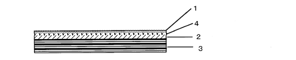
- 1 to 4 schematically show some embodiments of an SOI substrate of the present invention, in which 1 is a silicon substrate, 2 is a carbon film, and 3 is a microcrystalline diamond film. Reference numerals 4 denote silicon oxide films, respectively. That is, FIG. 1 shows an SOI substrate in which the I layer is composed of the carbon film 2 and the microcrystalline diamond film 3.
- FIG. 2 shows the SOI substrate shown in FIG. 1 between the silicon substrate 1 and the carbon film 2. 1 having a silicon oxide film 4 is shown.
- 3 shows an SOI substrate in which the I layer is composed of the carbon film 2, the microcrystalline diamond film 3, and the carbon film 2.
- FIG. 4 shows the silicon substrate 1 and the carbon film in the SOI substrate shown in FIG. A film having a silicon oxide film 4 between 2 is shown.
- a carbon film is formed on a silicon substrate having a diameter of 30 cm or more by using the surface wave plasma vapor deposition method in order to adapt to the manufacturing process of an existing silicon semiconductor device.
- a homogeneous microcrystalline diamond film having a diameter of 30 cm or more on a formed substrate hereinafter, also referred to as “carbon film / silicon substrate”
- high thermal conductivity is achieved.
- W tungsten
- Ta tantalum
- the film can prevent a defect from being formed in silicon as a device manufacturing layer, and can reduce a leakage current.
- the microcrystalline diamond film has a thick film structure of 100 ⁇ m or more in order to increase the breakdown voltage.
- a microcrystalline diamond film is formed by hot filament vapor deposition on a carbon film having a high thermal conductivity and high withstand voltage function formed by surface wave plasma vapor deposition.
- the carbon film As a film having a function of preventing the filament material from being mixed into silicon and having a high pressure resistance and high thermal conductivity, the carbon film has a flat surface and also has a high pressure resistance and high thermal conductivity function. Although it is the most suitable film, in addition to the carbon film, a silicon oxide film, an aluminum nitride film, a silicon nitride film, or the like can also be used as having the same function.
- one of the methods for manufacturing an SOI substrate of the present invention is to form a carbon film having a flat surface at an atomic level and a function of preventing entry into silicon, high pressure resistance, and high thermal conductivity on a silicon substrate.
- This is a method comprising a step of forming a film and a step of forming a microcrystalline diamond on the carbon film / silicon substrate obtained in the previous step by a hot filament vapor phase growth method. (See FIG. 1).
- the method for forming the silicon oxide film can be selected from the formation by a thermal oxidation method, a known film formation method such as a vapor phase growth method and a sputtering method.
- a carbon film having a flat surface at the atomic level and a function of high pressure resistance and high thermal conductivity after the above-described microcrystalline diamond film forming step is used.
- an SOI substrate having a hybrid structure (carbon film / microcrystalline diamond film / carbon film) of a carbon film and a microcrystalline diamond film having a high withstand voltage and high thermal conductivity can be produced (FIGS. 3 and 4). reference).
- a homogeneous microcrystalline diamond film with a diameter of 30 cm or more is laminated on the silicon / carbon film substrate with a diameter of 30 cm or more. It is also possible by the method.
- a mechanical polishing method is used to flatten the diamond surface. When this mechanical polishing is used on the carbon film surface of the silicon / carbon film substrate, defects and strains are generated in the silicon substrate for manufacturing the device. For this reason, it is necessary to form a carbon film formed on the silicon substrate by a surface wave plasma vapor deposition method that can form a flat surface at the atomic level in a self-organized manner.
- the microcrystalline diamond film requires an area of 30 cm or more in diameter
- synthesis by a hot filament vapor phase growth method can be used.
- the interface side of the microcrystalline diamond film with the substrate can be used as a bonding surface.
- an SOI substrate having a hybrid structure of carbon film / microcrystalline diamond film by the bonding method described above will be specifically described.
- a carbon film having a flat surface at an atomic level is formed on a silicon substrate by surface wave plasma vapor deposition to produce a carbon film / silicon substrate.
- a microcrystalline diamond film is formed on another silicon substrate by hot filament vapor deposition, and the silicon substrate is removed to form atoms formed at the interface between silicon and microcrystalline diamond. A level microcrystalline diamond surface is obtained.
- the obtained flat surface at the atomic level is bonded to the carbon film surface of the carbon film / silicon substrate.
- the carbon film surface and the microcrystalline diamond surface can be cleaned using an ion beam or plasma, and the carbon film surface and the microcrystalline diamond surface can be bonded together by a vacuum pressure bonding method.
- yet another method for manufacturing an SOI substrate according to the present invention includes (1) a step of first forming a carbon film having a flat surface at an atomic level on a silicon substrate by surface wave plasma vapor deposition.
- a method comprising a step of bonding a flat surface at an atomic level to the surface of the carbon film, and the method has a hybrid structure of a carbon film / microcrystalline diamond film having a high breakdown voltage and high thermal conductivity.
- An SOI substrate can be created.
- a carbon film / silicon substrate is bonded to a silicon substrate and a carbon substrate by bonding a microcrystalline diamond film formed by a hot filament vapor deposition method or a hot filament vapor deposition method.
- An SOI substrate for power semiconductors having no heat active defects and impurities and having excellent heat dissipation characteristics is produced at the interface of the film.
- the SOI substrate of the present invention has a hybrid structure of a carbon film and a microcrystalline diamond film.
- the hybrid structure of the carbon film and the microcrystalline diamond film is a diamond thin film formed by CVD, such as tungsten or tantalum. Therefore, it is possible to combine with power semiconductor devices (silicon carbide, gallium nitride, aluminum gallium nitride) other than silicon semiconductor.
- power semiconductor devices silicon carbide, gallium nitride, aluminum gallium nitride
- a hybrid structure of a carbon film and a microcrystalline diamond film can be directly formed on a semiconductor material such as silicon carbide or gallium nitride. As in the case of, it can be realized by a bonding technique used in a semiconductor process.
- ⁇ Electrical insulation> As a sample used for evaluation of electrical insulation, a sample in which an electrode having a diameter of 30 ⁇ m was formed on a microcrystalline diamond film of an SOI substrate of the present invention was used. The silicon of the SOI substrate was placed in a copper sample holder using a conductive silver paste. The measurement was performed by measuring current-voltage characteristics in a vacuum of 5 ⁇ 10 ⁇ 7 Torr. The value obtained by dividing the applied voltage by the total thickness of the microcrystalline diamond film and the carbon film was defined as the electric field, and the electric insulation was evaluated using the current-electric field characteristics. The larger the electric field where current is observed, the higher the electrical insulation.
- the thermal conductivity was measured by a thermoreflectance method.
- the silicon substrate of the SOI substrate was removed with a mixed solution of hydrofluoric acid and nitric acid to produce a self-stereoscopic structure of a microcrystalline diamond film / carbon film.
- a molybdenum thin film having a thickness of 100 nm was formed on the microcrystalline diamond surface and the carbon film surface by sputtering.
- the thermal conductivity in the direction perpendicular to the laminating direction and the laminating direction (in-plane direction) of the laminate was evaluated.
- Example 1 A 4-inch diameter wafer-like silicon substrate was used as the substrate. In order to increase the nucleation density of the carbon particles and form a uniform film, a pretreatment (nanocrystal diamond particle adhesion treatment) was performed on the substrate before the film formation.
- a colloidal solution (product name: Nanoamand, manufactured by Nano Carbon Laboratory Co., Ltd.) in which nanocrystal diamond particles having an average particle size of 5 nm are dispersed in pure water, or nanocrystal diamond particles having an average particle size of 30 nm or 40 nm (Tomei) Diamond Co., Ltd., product names MD30 and MD40) dispersed in pure water, or cluster diamond particles or graphite cluster diamond particles (Tokyo Diamond Tool Co., Ltd., product names CD and GCD, respectively), or Adamantane or a derivative thereof or a derivative thereof (each made by Idemitsu Kosan Co., Ltd.) solution was used, and the substrate was immersed in an ultrasonic cleaner.
- nanoamand manufactured by Nano Carbon Laboratory Co., Ltd.
- the substrate is immersed in ethanol for ultrasonic cleaning and dried, or these solutions are uniformly applied on the substrate by spin coating and dried.
- the uniformity of this pretreatment affects the uniformity of the carbon film after film formation.
- the number of diamond particles adhering on the substrate was 10 10 to 10 11 per cm 2 .
- the source gas a mixed gas of CH 4 , CO 2 and H 2 was used, and the concentrations of CH 4 and CO 2 were each 1 mol%.
- the gas pressure in the reaction vessel is 1.0 to 1.2 ⁇ 10 2 Pa (1.0 to 1.2 mbar), which is lower than the pressure (10 3 to 10 4 Pa) usually used for CVD synthesis of diamond, and a total of 20 A large area and uniform plasma was generated in a region wider than the substrate area by applying a microwave of ⁇ 24 kW.
- the substrate temperature during film formation can be maintained at 450 ° C. or less by adjusting the distance between the substrate and the antenna by closely contacting the Mo sample stage and the cooling stage.
- Film formation was performed for 6 hours under the above film formation conditions. A uniform and transparent carbon film was formed on the glass substrate after film formation. The film thickness was 200 nm.
- a microcrystalline diamond film was formed on the surface of the carbon film by a hot filament vapor deposition method.
- a hot filament vapor phase growth apparatus a large-area HFCVD apparatus (Sp3 Model 650) was used. Tungsten (W) was used as the filament, and the film was formed for 6 hours at a filament temperature of 2000 ° C. and a substrate temperature of 800 ° C. The film thickness was about 10 ⁇ m.
- the SOI substrate obtained in Example 1 has the structure shown in FIG.
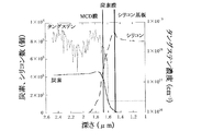
- FIG. 5 shows the evaluation results of impurities in the silicon of the SOI substrate obtained in Example 1. Tungsten was not observed in the carbon film and the silicon substrate, and it was found that the carbon film has a role to prevent tungsten from being mixed during the formation of the microcrystalline diamond film.
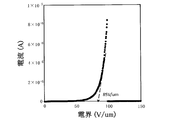
- Example 1 the current-electric field characteristics of the SOI substrate obtained in Example 1 are shown in FIG. Assuming that the electric field at which the current rapidly increases is the threshold electric field, the threshold electric field was 85 V / ⁇ m. This value is almost the same as the dielectric breakdown electric field (1 MV / cm) of single crystal diamond.
- the thermal conductivity of the SOI substrate obtained in Example 1 was 250 W / mK in the stacking direction and 110 W / mK in the direction perpendicular to the stacking direction. This value is almost the same as the reported value of microcrystalline diamond, which is one digit higher than the previously reported carbon film.
- Example 2 An SOI substrate was fabricated in the same manner as in Example 1 except that a silicon substrate on which a silicon oxide film (SiO 2 film) (thickness 20 nm) was formed was used. The structure of the SOI substrate obtained in Example 2 is shown in FIG.
- FIG. 7 shows the result of evaluating impurities in the silicon of the SOI substrate obtained in Example 2. Tungsten was not observed in the carbon film, silicon oxide film (SiO 2 film), or silicon substrate, and it was found that the carbon film has a role of preventing the entry of tungsten during the formation of the microcrystalline diamond film.
- Example 2 the current-electric field characteristics of the SOI substrate obtained in Example 2 are shown in FIG. Assuming that the electric field at which the current rapidly increases is the threshold electric field, the threshold electric field was 92 V / ⁇ m. This value is almost the same as the dielectric breakdown electric field (1 MV / cm) of single crystal diamond.
- An excellent SOI substrate for power semiconductor devices can be manufactured.
- FIG. 9 shows the results of impurity evaluation in silicon of the SOI substrate obtained in Comparative Example 1. Tungsten was observed at the interface between the microcrystalline diamond film and the silicon substrate, and was detected in the silicon substrate to a depth of 0.5 ⁇ m from the interface.
- FIG. 10 shows the current-electric field characteristics of the SOI substrate obtained in Comparative Example 1. Assuming that the electric field at which the current rapidly increases is the threshold electric field, the threshold electric field was 40 V / ⁇ m. This value was half of the dielectric breakdown electric field (100 V / ⁇ m) of single crystal diamond.
- the electric field where the leakage current of the SOI substrate of Example 1 is observed is that the SOI substrate having a hybrid structure of a carbon film and a microcrystalline diamond hybrid film as an I layer is Comparative Example 1. Compared with SOI using only the microcrystalline diamond film as an insulating layer, the electric field in which leakage current was observed increased twice. Therefore, it can be seen that an SOI substrate having a hybrid structure of a carbon film and a microcrystalline diamond film as an I layer can ensure insulation with a thickness half that of a microcrystalline diamond film alone. .
- Example 3 In Example 1 and Example 2, by forming a similar 200 nm carbon film on the microcrystalline diamond film, the electric field at which leakage current was observed was doubled. That is, it can be seen that by forming the structures of FIGS. 3 and 4, an SOI substrate having a leakage electric field of about 120 V / ⁇ m and about 130 V / ⁇ m can be manufactured. Further, the thermal conductivity was improved by 8 times in the film forming direction of the value of the carbon film and 3 times in the direction perpendicular to the film forming direction (in-plane direction).
- the SOI substrate having a hybrid structure of a carbon film and a microcrystalline diamond film or a film having a hybrid structure of a carbon film and a microcrystalline diamond film according to the present invention has a high insulating property and a high thermal conductivity. This is a very important technology because it can be used for all power semiconductor devices such as electric vehicles, hybrid vehicles, and inverters for motor control.
Landscapes
- Recrystallisation Techniques (AREA)
- Chemical Vapour Deposition (AREA)
Abstract
Description
一方、表面波プラズマ気相成長法により、直径30cm程度の面積に均一な炭素膜を形成する技術が、特許文献1および特許文献2に開示されている。この方法を用いて作成したSOI基板上に、集積回路(LSI)用途を目的とした電界効果トランジスタが試作され、動作が確認されている(非特許文献3)。
一方、前述の表面波プラズマ気相成長法により形成された炭素膜は高熱伝導性かつ高絶縁性という優れた特性を有するもの、該炭素膜をI層として用いたSOI基板上にパワー半導体デバイスを作製することで、レアメタルフリーで冷却機構を有しないデバイス実現する場合、表面波プラズマ気相成長法で合成した炭素膜の膜厚が数100nmと薄いために熱伝導度が数10W/mKであって充分なものとはいえず、パワー半導体デバイスへの応用は難しいという課題がある。
本発明は、これらの知見に基づいて完成するに至ったものであり、以下のとおりのものである。
[2]前記ハイブリット構造が、炭素膜/マイクロ結晶ダイヤモンド膜で構成されていることを特徴とする前記[1]のSOI基板。
[3]前記ハイブリット構造が、炭素膜/マイクロ結晶ダイヤモンド膜/炭素膜で構成されていることを特徴とする前記[1]のSOI基板。
[4]前記炭素膜が、表面波プラズマ気相成長法で形成された膜であることを特徴とする前記[1]~[3]のいずれかのSOI基板。
[5]前記マイクロ結晶ダイヤモンド膜が、熱フィラメント気相成長法で形成された膜であることを特徴とする前記[1]~[4]のいずれかのSOI基板。
[6]前記炭素膜上に、熱フィラメント気相成長法によりマイクロ結晶ダイヤモンド膜が形成されていることを特徴とする前記[1]~[5]のいずれかのSOI基板。
[7]前記炭素膜上に、熱フィラメント気相成長法で形成されたマイクロ結晶ダイヤモンド膜を張り合わせることにより形成されたことを特徴とする前記[5]のSOI基板。
[8]シリコン基板と炭素膜の界面にシリコン酸化膜を有することを特徴とする前記[1]~[7]のいずれかのSOI基板。
図1~図4は、本発明のSOI基板の実施形態の幾つかを模式的に示すものであって、図中、1は、シリコン基板、2は、炭素膜、3は、マイクロ結晶ダイヤモンド膜、4は、シリコン酸化膜、をそれぞれ示している。
すなわち、図1は、I層が、炭素膜2及びマイクロ結晶ダイヤモンド膜3からなるSOI基板を示しており、図2は、図1に示すSOI基板において、シリコン基板1と炭素膜2の間に、シリコン酸化膜4を有するものを示している。また、図3は、I層が、炭素膜2、マイクロ結晶ダイヤモンド膜3及び炭素膜2からなるSOI基板を示しており、図4は、図3に示すSOI基板において、シリコン基板1と炭素膜2の間に、シリコン酸化膜4を有するものを示している。
炭素膜とマイクロ結晶ダイヤモンド膜を張り合わせるためには、両膜の張り合わせ面が、原子レベルで平坦であることが必要条件である。一般的に、ダイヤモンド表面の平坦化には、機械的な研磨方法が用いられている。
この機械的研磨を、シリコン/炭素膜基板の炭素膜表面に用いた場合、デバイスを作製するシリコン基板に欠陥やひずみが生じてしまう。このため、原子レベルで平坦な表面が自己組織化的に形成できる表面波プラズマ気相成長法により成膜された炭素膜を、シリコン基板上に形成する必要がある。
(1)まずシリコン基板に表面波プラズマ気相成長法で、原子レベルで平坦な表面を有する炭素膜を成膜し、炭素膜/シリコン基板を製造する。
(2)次に、熱フィラメント気相成長法で、別のシリコン基板上にマイクロ結晶ダイヤモンド膜を成膜し、シリコン基板を除去することで、シリコンとマイクロ結晶ダイヤモンドの界面に形成された、原子レベルで平坦なマイクロ結晶ダイヤモンド表面を得る。
(3)次いで、得られた原子レベルで平坦な表面を、前記炭素膜/シリコン基板の炭素膜表面に張り合わせる。張り合わせには、イオンビームやプラズマを用いて該炭素膜表面およびマイクロ結晶ダイヤモンド表面洗浄を行い、真空加圧貼付け方式で、炭素膜表面とマイクロ結晶ダイヤモンド表面とを張り合わせることができる。
したがって、本発明のSOI基板の作製方法のさらにもう1つは、(1)まずシリコン基板に表面波プラズマ気相成長法で、原子レベルで平坦な表面を有する炭素膜を成膜する工程と、(2)熱フィラメント気相成長法で、シリコン基板上にマイクロ結晶ダイヤモンド膜を成膜し、機械的研磨方法で、マイクロ結晶ダイヤモンド表面を原子レベルでの平坦化とシリコンの除去を行う工程と、(3)の原子レベルで平坦な表面を、前記炭素膜表面に張り合わせる工程とからなる方法であり、該方法により、高耐圧かつ高熱伝導性の炭素膜/マイクロ結晶ダイヤモンド膜のハイブリット構造を有するSOI基板が作成できる。
なお、実施例における炭素膜の製造方法は、特許文献1および特許文献2で開示されている方法を用いた。
《不純物評価》
本発明のSOI基板のシリコン基板中のタングステンの評価は、二次イオン質量分析法により行った。測定は、一次イオンにO2 +を用い、加速電圧を3kVとした。測定時の真空度は3×10⁻⁹Torrである。
電気絶縁性の評価に用いた試料として、本発明のSOI基板のマイクロ結晶ダイヤモンド膜上に直径30μmの電極を形成したものを用いた。SOI基板のシリコンは導電性の銀ペーストを用いて銅製の試料ホルダーに設置した。測定は、5×10⁻⁷Torrの真空中で、電流-電圧特性を測定した。印加電圧をマイクロ結晶ダイヤモンドの膜厚と炭素膜の膜厚の合計膜厚で割った値を電界とし、電流-電界特性を用いて、電気絶縁性を評価した。電流が観測される電界が大きい程電気絶縁性が高いことを意味する。
熱伝導度の測定は、サーモリフレクタンス法で評価した。試料は、SOI基板のシリコン基板をフッ酸と硝酸の混合液で除去し、マイクロ結晶ダイヤモンド膜/炭素膜の自立体構造を作製した。このマイクロ結晶ダイヤモンド/炭素膜自立体構造マイクロ結晶ダイヤモンド面と炭素膜面にスパッタリング法で厚さ100nmのモリブデン薄膜を形成した。
熱伝導度は、積層体の積層方向および積層方向に対して垂直方向(面内方向)の熱伝導度を評価した。
基板として4インチ径のウェハ状のシリコン基板を用いた。炭素粒子の核形成密度を高め均一な成膜とするために、成膜前の基板に前処理(ナノクリスタルダイヤモンド粒子付着処理)を行った。
この前処理には平均粒径5nmのナノクリスタルダイヤモンド粒子を純水中に分散させたコロイド溶液(有限会社ナノ炭素研究所製 製品名ナノアマンド)または平均粒径30nm又は40nmのナノクリスタルダイヤモンド粒子(トーメイダイヤ株式会社製 製品名各々MD30およびMD40)を純水中に分散させた溶液、あるいはクラスターダイヤモンド粒子またはグラファイトクラスターダイヤモンド粒子(東京ダイヤモンド工具製作所製 製品名各々CDおよびGCD)を分散させたエタノール、あるいはアダマンタンまたはその誘導体あるいはそれらの誘導体(各々出光興産株式会社製)溶液を用い,これに基板を浸して超音波洗浄器にかけた。
その後、基板をエタノール中に浸して超音波洗浄を行い、乾燥させるか、またはこれらの溶液をスピンコートによって基板上に均一に塗布し、乾燥させる。この前処理の均一性が成膜後の炭素膜の均一性に影響する。この場合、基板上に付着するダイヤモンド粒子は、1cm2当たり、1010~1011個であった。
以上の成膜条件の下、6時間成膜を行った。成膜後のガラス基板上には、均一かつ透明な炭素膜が形成された。この膜の膜厚は、200nmであった。
基板として、シリコン酸化膜(SiO2膜)(厚さ20nm)を形成したシリコン基板を用いた以外は、実施例1と同様にしてSOI基板を作製した。実施例2で得られたSOI基板の構造を図2に示す。
マイクロ結晶ダイヤモンドのみをI層(絶縁層)としたSOI基板を作製した。基板には、シリコン基板を用いた。
マイクロ結晶ダイヤモンド膜の成膜の前処理として、ダイヤモンド粒子でシリコン基板に傷付け処理をおこなった。熱フィラメント気相成長装置は、大面積HFCVD装置(sp3社製 Model 650)を用いた。フィラメントにはタングステン(W)を用い、フィラメント温度2000℃、基板温度800℃で、6時間の成膜をおこなった。この膜の膜厚は、約10μmであった。
実施例1及び実施例2において、マイクロ結晶ダイヤモンド膜に、さらに同様の200nmの炭素膜を形成することで、リーク電流が観測される電界が2倍となった。つまり、図3および図4の構造を形成することで、リーク電界が約120V/μmおよび約130V/μmのSOI基板が作製できることがわかる。また、熱伝導性は、炭素膜の値の成膜方向は8倍、成膜方向と垂直方向(面内方向)は3倍と改善された。
2:炭素膜
3:マイクロ結晶ダイヤモンド膜
4:シリコン酸化膜
Claims (8)
- SOI基板の絶縁層が、炭素膜とマイクロ結晶ダイヤモンド膜のハイブリット構造を有することを特徴とするSOI基板。
- 前記ハイブリット構造が、炭素膜/マイクロ結晶ダイヤモンド膜で構成されていることを特徴とする請求項1に記載のSOI基板。
- 前記ハイブリット構造が、炭素膜/マイクロ結晶ダイヤモンド膜/炭素膜で構成されていることを特徴とする請求項1に記載のSOI基板。
- 前記炭素膜が、表面波プラズマ気相成長法で形成された膜であることを特徴とする請求項1~3のいずれか1項に記載のSOI基板。
- 前記マイクロ結晶ダイヤモンド膜層が、熱フィラメント気相成長法で形成された膜であることを特徴とする請求項1~4のいずれか1項に記載のSOI基板。
- 前記炭素膜上に、熱フィラメント気相成長法によりマイクロ結晶ダイヤモンド膜が形成されていることを特徴とする請求項1~5のいずれか1項に記載のSOI基板。
- 前記炭素膜上に、熱フィラメント気相成長法で形成されたマイクロ結晶ダイヤモンド膜を張り合わせることにより形成されたことを特徴とする請求項5に記載のSOI基板。
- シリコン基板と炭素膜の界面にシリコン酸化膜を有することを特徴とする請求項1~7のいずれか1項に記載のSOI基板。
Priority Applications (2)
| Application Number | Priority Date | Filing Date | Title |
|---|---|---|---|
| DE112011103476T DE112011103476T5 (de) | 2010-10-14 | 2011-10-12 | SOI-Substrat |
| JP2012538690A JP5665202B2 (ja) | 2010-10-14 | 2011-10-12 | Soi基板 |
Applications Claiming Priority (2)
| Application Number | Priority Date | Filing Date | Title |
|---|---|---|---|
| JP2010231041 | 2010-10-14 | ||
| JP2010-231041 | 2010-10-14 |
Publications (1)
| Publication Number | Publication Date |
|---|---|
| WO2012050122A1 true WO2012050122A1 (ja) | 2012-04-19 |
Family
ID=45938349
Family Applications (1)
| Application Number | Title | Priority Date | Filing Date |
|---|---|---|---|
| PCT/JP2011/073412 Ceased WO2012050122A1 (ja) | 2010-10-14 | 2011-10-12 | Soi基板 |
Country Status (3)
| Country | Link |
|---|---|
| JP (1) | JP5665202B2 (ja) |
| DE (1) | DE112011103476T5 (ja) |
| WO (1) | WO2012050122A1 (ja) |
Cited By (1)
| Publication number | Priority date | Publication date | Assignee | Title |
|---|---|---|---|---|
| JPWO2020250815A1 (ja) * | 2019-06-14 | 2020-12-17 |
Citations (4)
| Publication number | Priority date | Publication date | Assignee | Title |
|---|---|---|---|---|
| JPS63150926A (ja) * | 1986-12-15 | 1988-06-23 | Ricoh Co Ltd | ダイヤモンド状炭素膜の製膜法 |
| JP2006228963A (ja) * | 2005-02-17 | 2006-08-31 | Kobe Steel Ltd | 半導体ウエハの製造方法 |
| WO2008057055A1 (en) * | 2006-11-10 | 2008-05-15 | Agency For Science, Technology And Research | A micromechanical structure and a method of fabricating a micromechanical structure |
| JP2010202911A (ja) * | 2009-03-02 | 2010-09-16 | Mitsubishi Materials Corp | 炭素膜、炭素膜の製造方法及びcmpパッドコンディショナー |
Family Cites Families (3)
| Publication number | Priority date | Publication date | Assignee | Title |
|---|---|---|---|---|
| JP4538587B2 (ja) * | 2004-04-19 | 2010-09-08 | 独立行政法人産業技術総合研究所 | 積層体及びその製造方法並びに該積層体を備えた光デバイス、光学ガラス、腕時計、電子回路基板、研磨用工具 |
| WO2007004647A1 (ja) | 2005-07-04 | 2007-01-11 | National Institute Of Advanced Industrial Science And Technology | 炭素膜 |
| JP2011241463A (ja) * | 2010-05-20 | 2011-12-01 | Toyota Motor Corp | 硬質炭素膜層を備えた層構造体およびその層構造を表面に備えたバルブリフター |
-
2011
- 2011-10-12 WO PCT/JP2011/073412 patent/WO2012050122A1/ja not_active Ceased
- 2011-10-12 DE DE112011103476T patent/DE112011103476T5/de not_active Withdrawn
- 2011-10-12 JP JP2012538690A patent/JP5665202B2/ja not_active Expired - Fee Related
Patent Citations (4)
| Publication number | Priority date | Publication date | Assignee | Title |
|---|---|---|---|---|
| JPS63150926A (ja) * | 1986-12-15 | 1988-06-23 | Ricoh Co Ltd | ダイヤモンド状炭素膜の製膜法 |
| JP2006228963A (ja) * | 2005-02-17 | 2006-08-31 | Kobe Steel Ltd | 半導体ウエハの製造方法 |
| WO2008057055A1 (en) * | 2006-11-10 | 2008-05-15 | Agency For Science, Technology And Research | A micromechanical structure and a method of fabricating a micromechanical structure |
| JP2010202911A (ja) * | 2009-03-02 | 2010-09-16 | Mitsubishi Materials Corp | 炭素膜、炭素膜の製造方法及びcmpパッドコンディショナー |
Cited By (4)
| Publication number | Priority date | Publication date | Assignee | Title |
|---|---|---|---|---|
| JPWO2020250815A1 (ja) * | 2019-06-14 | 2020-12-17 | ||
| WO2020250815A1 (ja) * | 2019-06-14 | 2020-12-17 | Tdk株式会社 | 電子部品内蔵基板及びこれを用いた回路モジュール |
| JP7439833B2 (ja) | 2019-06-14 | 2024-02-28 | Tdk株式会社 | 電子部品内蔵基板及びこれを用いた回路モジュール |
| US12243841B2 (en) | 2019-06-14 | 2025-03-04 | Tdk Corporation | Electronic component embedded substrate and circuit module using the same |
Also Published As
| Publication number | Publication date |
|---|---|
| JPWO2012050122A1 (ja) | 2014-02-24 |
| JP5665202B2 (ja) | 2015-02-04 |
| DE112011103476T5 (de) | 2013-08-01 |
Similar Documents
| Publication | Publication Date | Title |
|---|---|---|
| CN113690298A (zh) | 半导体复合衬底、半导体器件及制备方法 | |
| CN109722641B (zh) | 金刚石/石墨烯复合导热膜及其制备方法和散热系统 | |
| US11139427B2 (en) | Bonded body and elastic wave element | |
| JP2018049868A (ja) | 半導体積層構造体および半導体デバイス | |
| WO2013002212A1 (ja) | 複合基板およびその製造方法 | |
| JP2000331899A (ja) | Soiウェーハの製造方法およびsoiウェーハ | |
| JP2020105038A (ja) | 半導体基板、半導体基板の製造方法およびそれを用いた半導体装置 | |
| TW202015334A (zh) | 接合體及彈性波元件 | |
| CN104319447A (zh) | 一种基于石墨烯的多层共面波导传输线及其制备方法 | |
| JP2024147519A (ja) | 低い抵抗率の多結晶ベース基板又はウエハ | |
| JP2011529632A (ja) | 真性ダイアモンド層及びドープダイアモンド層で被覆されたセミコンダクター・オン・インシュレータ基板 | |
| JP5665202B2 (ja) | Soi基板 | |
| WO2024103727A1 (zh) | 碳化硅外延片及其制备方法和应用 | |
| KR20170093601A (ko) | 그래핀 코팅 방열부재의 제조방법과 이에 의하여 제조된 방열부재 | |
| CN113594110B (zh) | 一种半导体器件及其制备方法 | |
| KR20170056390A (ko) | 밴드갭을 갖는 그래핀 박막 제조방법 및 이에 의해 제조된 그래핀 박막을 포함하는 박막 트랜지스터 | |
| CN101872718B (zh) | 石墨烯晶片的制备方法 | |
| CN107785304A (zh) | 以氮化物薄膜为绝缘埋层的soi材料及其制备方法 | |
| JP2025065001A (ja) | 高抵抗率多結晶シリコンカーバイド(SiC)基板、及びその製造方法 | |
| Serikawa et al. | High-mobility poly-Si thin film transistors fabricated on stainless-steel foils by low-temperature processes using sputter-depositions | |
| US7148079B1 (en) | Diamond like carbon silicon on insulator substrates and methods of fabrication thereof | |
| CN118737992A (zh) | 导热复合组件及其制备方法和应用 | |
| CN116314274A (zh) | 一种具有p沟道的GaN基HEMT器件的制备方法 | |
| CN105977197A (zh) | 基于非晶化与尺度效应的SiN埋绝缘层上晶圆级单轴应变SiGe的制作方法 | |
| TWI743932B (zh) | 半導體基板及其製造方法 |
Legal Events
| Date | Code | Title | Description |
|---|---|---|---|
| 121 | Ep: the epo has been informed by wipo that ep was designated in this application |
Ref document number: 11832557 Country of ref document: EP Kind code of ref document: A1 |
|
| WWE | Wipo information: entry into national phase |
Ref document number: 1120111034768 Country of ref document: DE Ref document number: 112011103476 Country of ref document: DE |
|
| ENP | Entry into the national phase |
Ref document number: 2012538690 Country of ref document: JP Kind code of ref document: A |
|
| 122 | Ep: pct application non-entry in european phase |
Ref document number: 11832557 Country of ref document: EP Kind code of ref document: A1 |