WO2012043787A1 - 電気素子パッケージ - Google Patents
電気素子パッケージ Download PDFInfo
- Publication number
- WO2012043787A1 WO2012043787A1 PCT/JP2011/072527 JP2011072527W WO2012043787A1 WO 2012043787 A1 WO2012043787 A1 WO 2012043787A1 JP 2011072527 W JP2011072527 W JP 2011072527W WO 2012043787 A1 WO2012043787 A1 WO 2012043787A1
- Authority
- WO
- WIPO (PCT)
- Prior art keywords
- glass frit
- glass
- substrate
- organic
- electrode
- Prior art date
- Legal status (The legal status is an assumption and is not a legal conclusion. Google has not performed a legal analysis and makes no representation as to the accuracy of the status listed.)
- Ceased
Links
Images







Classifications
-
- C—CHEMISTRY; METALLURGY
- C03—GLASS; MINERAL OR SLAG WOOL
- C03C—CHEMICAL COMPOSITION OF GLASSES, GLAZES OR VITREOUS ENAMELS; SURFACE TREATMENT OF GLASS; SURFACE TREATMENT OF FIBRES OR FILAMENTS MADE FROM GLASS, MINERALS OR SLAGS; JOINING GLASS TO GLASS OR OTHER MATERIALS
- C03C8/00—Enamels; Glazes; Fusion seal compositions being frit compositions having non-frit additions
- C03C8/02—Frit compositions, i.e. in a powdered or comminuted form
- C03C8/08—Frit compositions, i.e. in a powdered or comminuted form containing phosphorus
-
- B—PERFORMING OPERATIONS; TRANSPORTING
- B65—CONVEYING; PACKING; STORING; HANDLING THIN OR FILAMENTARY MATERIAL
- B65D—CONTAINERS FOR STORAGE OR TRANSPORT OF ARTICLES OR MATERIALS, e.g. BAGS, BARRELS, BOTTLES, BOXES, CANS, CARTONS, CRATES, DRUMS, JARS, TANKS, HOPPERS, FORWARDING CONTAINERS; ACCESSORIES, CLOSURES, OR FITTINGS THEREFOR; PACKAGING ELEMENTS; PACKAGES
- B65D85/00—Containers, packaging elements or packages, specially adapted for particular articles or materials
-
- C—CHEMISTRY; METALLURGY
- C03—GLASS; MINERAL OR SLAG WOOL
- C03C—CHEMICAL COMPOSITION OF GLASSES, GLAZES OR VITREOUS ENAMELS; SURFACE TREATMENT OF GLASS; SURFACE TREATMENT OF FIBRES OR FILAMENTS MADE FROM GLASS, MINERALS OR SLAGS; JOINING GLASS TO GLASS OR OTHER MATERIALS
- C03C3/00—Glass compositions
- C03C3/12—Silica-free oxide glass compositions
- C03C3/16—Silica-free oxide glass compositions containing phosphorus
- C03C3/19—Silica-free oxide glass compositions containing phosphorus containing boron
-
- C—CHEMISTRY; METALLURGY
- C03—GLASS; MINERAL OR SLAG WOOL
- C03C—CHEMICAL COMPOSITION OF GLASSES, GLAZES OR VITREOUS ENAMELS; SURFACE TREATMENT OF GLASS; SURFACE TREATMENT OF FIBRES OR FILAMENTS MADE FROM GLASS, MINERALS OR SLAGS; JOINING GLASS TO GLASS OR OTHER MATERIALS
- C03C8/00—Enamels; Glazes; Fusion seal compositions being frit compositions having non-frit additions
- C03C8/24—Fusion seal compositions being frit compositions having non-frit additions, i.e. for use as seals between dissimilar materials, e.g. glass and metal; Glass solders
-
- H—ELECTRICITY
- H05—ELECTRIC TECHNIQUES NOT OTHERWISE PROVIDED FOR
- H05B—ELECTRIC HEATING; ELECTRIC LIGHT SOURCES NOT OTHERWISE PROVIDED FOR; CIRCUIT ARRANGEMENTS FOR ELECTRIC LIGHT SOURCES, IN GENERAL
- H05B33/00—Electroluminescent light sources
- H05B33/02—Details
- H05B33/04—Sealing arrangements, e.g. against humidity
-
- H—ELECTRICITY
- H10—SEMICONDUCTOR DEVICES; ELECTRIC SOLID-STATE DEVICES NOT OTHERWISE PROVIDED FOR
- H10K—ORGANIC ELECTRIC SOLID-STATE DEVICES
- H10K50/00—Organic light-emitting devices
- H10K50/80—Constructional details
- H10K50/84—Passivation; Containers; Encapsulations
- H10K50/842—Containers
- H10K50/8426—Peripheral sealing arrangements, e.g. adhesives, sealants
-
- H—ELECTRICITY
- H10—SEMICONDUCTOR DEVICES; ELECTRIC SOLID-STATE DEVICES NOT OTHERWISE PROVIDED FOR
- H10K—ORGANIC ELECTRIC SOLID-STATE DEVICES
- H10K50/00—Organic light-emitting devices
- H10K50/80—Constructional details
- H10K50/84—Passivation; Containers; Encapsulations
- H10K50/844—Encapsulations
- H10K50/8445—Encapsulations multilayered coatings having a repetitive structure, e.g. having multiple organic-inorganic bilayers
-
- H—ELECTRICITY
- H10—SEMICONDUCTOR DEVICES; ELECTRIC SOLID-STATE DEVICES NOT OTHERWISE PROVIDED FOR
- H10K—ORGANIC ELECTRIC SOLID-STATE DEVICES
- H10K50/00—Organic light-emitting devices
- H10K50/80—Constructional details
- H10K50/85—Arrangements for extracting light from the devices
- H10K50/858—Arrangements for extracting light from the devices comprising refractive means, e.g. lenses
-
- H—ELECTRICITY
- H10—SEMICONDUCTOR DEVICES; ELECTRIC SOLID-STATE DEVICES NOT OTHERWISE PROVIDED FOR
- H10K—ORGANIC ELECTRIC SOLID-STATE DEVICES
- H10K59/00—Integrated devices, or assemblies of multiple devices, comprising at least one organic light-emitting element covered by group H10K50/00
- H10K59/80—Constructional details
- H10K59/87—Passivation; Containers; Encapsulations
- H10K59/871—Self-supporting sealing arrangements
- H10K59/8722—Peripheral sealing arrangements, e.g. adhesives, sealants
Definitions
- the present invention relates to an electric element package in which an electric element sensitive to the surrounding environment such as an organic EL is hermetically sealed in order to prevent deterioration due to oxygen or moisture in the surrounding environment.
- organic EL display devices organic EL displays
- organic EL displays have been researched and developed, and have already been put into practical use in some fields such as small display devices used for mobile phones and the like.
- the organic EL element (organic EL layer) used in this organic EL display device is a sensitive element that easily deteriorates when exposed to oxygen and moisture in the surrounding environment. Therefore, in practical use, the organic EL layer is incorporated in an organic EL display device in a hermetically sealed state, thereby maintaining the display quality of the device and extending its life.
- the sealing substrate is disposed oppositely on the element substrate on which the organic EL layer is disposed, and is disposed on the element substrate in this state.
- the gap between the element substrate and the sealing substrate is hermetically sealed with glass frit so as to surround the periphery of the organic EL layer.
- the glass frit is heated and softened by irradiating laser light from the sealing substrate side, so that the glass frit is welded to the element substrate and the sealing substrate to form an airtight sealing structure.
- an electrode for example, an ITO electrode
- an electrode for supplying electric power to the organic EL layer from the outside by the irradiation heat of the laser light or the organic EL layer may be damaged.
- an electrode for supplying electric power from the outside to the organic EL layer is disposed below the glass frit. Therefore, if no thermal countermeasures are taken against the heat of laser light irradiation, the electrode located under the glass frit is undesirably heated by the heat of laser light irradiation, resulting in thermal damage and possibly disconnection. is there. Further, when the electrode is heated in this manner, the heat is transmitted to the organic EL layer through the electrode, and there is a possibility that the organic EL layer may be thermally damaged.
- Patent Documents 1 and 2 a metal layer and an improvement layer for improving adhesive strength are arranged on the substrate side where the organic EL element is arranged, and glass frit is welded to the improvement layer.
- the substrate on which the organic EL layer is disposed and the substrate opposite to the substrate are bonded.
- Patent Documents 1 and 2 when a metal layer functioning as a reflective film that reflects laser light is used, if a glass frit is directly welded to the metal layer, the adhesive force between the two Cannot be maintained sufficiently. Therefore, it is essential to interpose an improvement layer for improving the adhesive force between the metal layer and the glass frit.
- the metal layer when the metal layer is in contact with the electrode connected to the organic EL element, there is a problem that the metal layer and the electrode are electrically connected to each other. Therefore, an insulating layer is provided between the metal layer and the electrode. It is essential to intervene. Therefore, the problem that the freedom degree of design of an organic EL element package falls may arise.
- the organic EL element has been described as an example.
- an electric element other than the organic EL element is easily affected by the external environment and can be used by being hermetically sealed with a glass frit. Problems can arise. Further, not only the display device but also other fields such as a lighting device and a solar battery may cause the same problem when using the electric element package.
- the present invention makes it possible to damage the electrodes and the electric elements as much as possible by the irradiation heat of the laser light applied when the glass frit is welded while ensuring the degree of freedom in designing the electric element packages. It is a technical problem to reduce it to a minimum.
- the present invention devised to solve the above problems includes an element substrate on which an electric element is arranged, a sealing substrate facing the surface of the element substrate on the electric element side with a space therebetween, and the electric element.
- an electronic device package having a glass frit that hermetically seals a gap between the device substrate and the sealing substrate so as to surround the periphery
- the electronic device package is disposed between the device substrate and the glass frit, and the glass frit is It is characterized by having a protective film for protecting the electrode from laser light irradiated during welding.
- this invention includes the 1st invention shown below and the 2nd invention as a specific example.
- an element substrate on which an electric element is arranged, a sealing substrate facing the electric element side surface of the element substrate with a space therebetween, and the element substrate so as to surround the electric element.
- a glass frit that hermetically seals a gap between the sealing substrate and the reflective substrate that is disposed between the element substrate and the glass frit and reflects a laser beam irradiated when the glass frit is welded
- the reflective film is characterized by comprising a dielectric multilayer film in which low-refractive index dielectric layers and high-refractive index dielectric layers are alternately stacked.
- the dielectric film in which the reflection film that reflects the laser light irradiated when the glass frit is welded is formed by alternately laminating low refractive index dielectric layers and high refractive index dielectric layers. Formed from a film. Since the dielectric layer constituting the dielectric multilayer film has excellent adhesion to the glass frit, in addition to the dielectric multilayer film, only a new adhesive strength improvement has been made to increase the adhesion to the glass frit. Even without providing a layer, it is possible to maintain good adhesion with the glass frit.
- the dielectric layers constituting the dielectric multilayer film are not electrically conductive, it is possible to maintain electrical insulation between the electrodes connected to the electric elements without providing an insulating layer separately. It becomes. Therefore, since it is not an essential condition to separately provide an adhesive strength improving layer for improving the adhesive strength with the glass frit or an insulating layer, a degree of freedom in designing the electric element package is ensured.
- the dielectric multilayer film as described above by adjusting the material selection and film thickness of each of the low refractive index dielectric layer and the high refractive index dielectric layer, A high reflectance can be easily realized. Therefore, when laser light is irradiated during frit glass welding, the laser light is reliably reflected to the frit glass side by the dielectric multilayer film, and is effectively used for heating the frit glass. Therefore, the laser light that passes through the dielectric multilayer film and irradiates the electrodes and the like is reduced as much as possible, so that it is ensured that the electrodes and electrical elements are unduly heated by the laser light and cause thermal damage. Can be prevented.
- the dielectric multilayer film may be directly welded to the glass frit, or the dielectric multilayer film may be directly formed on the electrode connected to the electric element.
- the dielectric multilayer film has a high adhesive force with the glass frit and has an insulating property. Therefore, the dielectric multilayer film is directly welded to the glass frit or formed directly on the electrode connected to the electric element. can do. In this way, the configuration of the electric element package is simplified, and the manufacture becomes easy.
- the refractive index of the low refractive index dielectric layer is preferably 1.6 or less, and the refractive index of the high refractive index dielectric layer is preferably 1.7 or more.
- the refractive index difference between the low refractive index dielectric layer and the high refractive index dielectric layer can be kept moderate, and the reflectance with respect to the laser beam can be maintained well.
- the dielectric multilayer film preferably has a reflectivity of 50% or more with respect to laser light.
- the glass frit may contain 80 to 99.7% by mass of inorganic powder containing SnO-containing glass powder and 0.3 to 20% by mass of pigment.
- SnO-containing glass powder means glass powder containing SnO in an amount of 20 mol% or more as a glass composition.
- the “inorganic powder” means an inorganic material powder other than the pigment, and usually means a mixture of glass powder and a refractory filler.
- the glass frit contains SnO-containing glass powder
- the softening point of the glass powder is lowered and the softening point of the entire glass frit is also lowered.
- this inorganic powder containing SnO containing glass powder is made into the said numerical range, since the softening point of a glass frit will fall moderately, welding (sealing) by a laser beam can be completed in a short time, and the welding strength Can also be increased. If the content of the inorganic powder is less than 80% by mass, the softening flow of the glass frit becomes poor when welding with laser light, and it becomes difficult to maintain high welding strength.
- the glass frit contains 0.3 to 20% by mass of pigment. If the pigment content is regulated to 0.3% by mass or more, the glass frit can easily absorb the laser beam, and the irradiation heat of the laser beam can be efficiently applied to the glass frit. Therefore, it becomes easy to locally heat only the part to be welded in the glass frit, and thermal damage to the electrode and the electric element can be prevented. On the other hand, if the pigment content is controlled to 20% by mass or less, it is possible to prevent the glass frit from devitrifying when the glass frit is welded by the irradiation heat of the laser beam.
- the SnO-containing glass powder may contain SnO 35 to 70% and P 2 O 5 10 to 30% in terms of glass composition.
- an element substrate on which the electric element is arranged, a sealing substrate facing the surface of the element substrate on the electric element side with a space therebetween, and the periphery of the electric element are surrounded.
- the electric element package having a glass frit that hermetically seals a gap between the element substrate and the sealing substrate, the electric element package is disposed between the element substrate and the glass frit and irradiated when the glass frit is welded. It is characterized by having a metal oxide film for protecting the electrode from laser light.
- the metal oxide film is formed between the element substrate and the glass frit. Therefore, when the glass frit is melted by irradiating the glass frit with laser light, that is, at the time of laser welding. It is possible to avoid the contact between the glass frit and the electrode as much as possible while suppressing the heat generated by the laser light irradiation.
- the thickness of the metal oxide film is preferably 10 to 500 nm. In this way, it is possible to reliably protect the electrode while preventing peeling between the glass frit and the metal oxide film after laser welding.
- the metal oxide film is preferably any one of SiO 2 , ZrO 2 , Y 2 O 3 , TiO 2 , Al 2 O 3 , Ta 2 O 5 , and Nb 2 O 5 . These metal oxide films are particularly excellent in adhesion to glass frit and insulation.
- the metal oxide film is preferably welded directly to the glass frit or formed directly on the electrode connected to the electric element.
- the configuration of the electric element package is simplified, and the manufacturing efficiency of the electric element package is improved.
- the metal oxide film is excellent in adhesion with the glass frit and insulative. For this reason, the metal oxide film can be directly welded to the glass frit, or the metal oxide film can be directly formed on the electrode connected to the electric element.
- the glass frit preferably contains 80 to 99.95% by mass of inorganic powder containing SnO-containing glass powder and 0.05 to 20% by mass of pigment. If it does in this way, since glass frit contains SnO containing glass powder, the softening point of glass powder will fall and the softening point of glass frit will also fall. And if the inorganic powder containing this SnO containing glass powder is made into the said numerical value range, since the softening point of a glass frit will fall moderately, laser welding can be completed in a short time and welding strength can also be raised.
- the SnO-containing glass powder contains 35% to 70% SnO and 10% to 30% P 2 O 5 in terms of glass composition. In this way, it becomes easy to improve the water resistance of the glass frit while maintaining the low melting point characteristics of the glass frit.
- the present invention it is possible to prevent the electrode and the electric element from being damaged as much as possible by the irradiation heat of the laser beam applied at the time of welding the glass frit while ensuring the degree of freedom in designing the electric element package. Can be reduced.
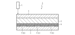
- FIG. 2 is a cross-sectional view taken along the line AA in FIG.
- FIG. 4 is a cross-sectional view taken along line AA in FIG. 3.
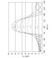
- It is a graph which shows the simulation result of the frequency characteristic of the reflectance in a dielectric multilayer film.
- It is a graph which shows the measurement result of the frequency characteristic of the reflectance in a dielectric multilayer.
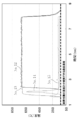
- It is a graph which shows the measurement result of the temperature of the electrode at the time of laser welding.
- FIG. 1 is a longitudinal sectional view showing a schematic configuration of an organic EL element package according to the present embodiment.
- the organic EL element package 1 includes an element substrate 3 on which an organic EL layer 2 is formed, a sealing substrate 4 facing the surface of the element substrate 3 on the organic EL layer 2 side with a space therebetween, and an organic EL layer 2.
- a glass frit 5 that hermetically seals (seals) the gap between the element substrate 3 and the sealing substrate 4 while surrounding the frame in a frame shape is provided as a basic configuration.
- the element substrate 3 and the sealing substrate 4 are made of, for example, a glass substrate having a plate thickness of 0.05 to 0.7 mm.
- the element substrate 3 is provided with a first electrode 6 and a second electrode 7 connected to both the front and back sides of the organic EL layer 2.
- the electrodes 6 and 7 are guided from the organic EL layer 2 to the outside of the package 1 through the lower part of the glass frit 5 to supply power to the organic EL layer 2.
- the electrodes 6 and 7 are branched according to a predetermined pattern as shown in FIG.
- the first electrode 6 on the back surface side of the organic EL layer 2 is formed of, for example, a transparent electrode film (ITO film), and the second electrode 7 on the surface side of the organic EL layer is formed of, for example, a metal electrode film such as aluminum. Formed with.
- Both the first electrode 6 and the second electrode 7 may be formed of a transparent electrode film.
- the glass frit 5 is irradiated from the sealing substrate 4 side with the laser light emitted from the laser L, and the glass frit 5 is heated and softened to thereby form the element substrate 3 and the sealing substrate.
- the package 1 is hermetically sealed.
- the laser L for example, an infrared laser (wavelength 700 to 2500 nm) is used.
- the electrodes 6 and 7 when the electrodes 6 and 7 are heated by the irradiation heat of the laser light during the welding of the glass frit 5, the electrodes 6 and 7 may be thermally damaged.
- the heat is transmitted to the organic EL layer 2 through the electrodes 6 and 7, and the organic EL layer 2 may be thermally damaged. Therefore, in the present embodiment, the dielectric multilayer film 8 functioning as a reflection film is interposed between the glass frit 5 and the electrodes 6 and 7, and the laser light is transmitted to the glass frit 5 on the opposite side of the electrodes 6 and 7. Reflected to the side.
- This dielectric multilayer film 8 is formed by alternately laminating low refractive index dielectric layers and high refractive index dielectric layers, and has a reflectance of 50% in the wavelength band (for example, 808 nm) of the laser light to be used. It is set above (preferably 90% or more).
- the low refractive index dielectric layer is formed of a material having a refractive index of 1.6 or less, preferably a refractive index of 1.33 to 1.6.
- these materials include silica (SiO 2 ), alumina (Al 2 O 3 ), lanthanum fluoride (LaF 3 ), magnesium fluoride (MgF 2 ), and aluminum hexafluoride sodium (Na 3 AlF 6 ). Is mentioned.
- the refractive index of the low refractive index dielectric layer is n1
- the thickness is d1
- the wavelength of the laser beam is ⁇
- the optical film thickness (n1 ⁇ d1) of the low refractive index dielectric layer is ⁇ / 4.
- the high refractive index dielectric layer is formed of a material having a refractive index of 1.7 or more, preferably a refractive index of 1.7 to 2.5.
- these materials include titanium oxide (TiO 2 ), zirconium oxide (ZrO 2 ), tantalum pentoxide (Ta 2 O 5 ), niobium pentoxide (Nb 2 O 5 ), and lanthanum oxide (La 2 O 3 ).
- the refractive index of the high refractive index dielectric layer is n2
- the thickness is d2
- the wavelength of the laser beam is ⁇
- the optical film thickness (n2 ⁇ d2) of the high refractive index dielectric layer is an integral multiple of ⁇ / 4. Is set to be Note that SiO 2 can be used when a laser beam with ⁇ of 1200 nm or more is used, and GeO 2 can be used when a laser beam with ⁇ of 1700 nm or more is used.
- the dielectric multilayer film 8 is preferably formed by laminating a total of four or more low refractive index dielectric layers and high refractive index dielectric layers.
- the dielectric multilayer film 8 preferably has different thermal expansion coefficients between the low refractive index dielectric layer and the high refractive index dielectric layer. In this way, compared to the case where the laser light reflecting film is formed as a single layer, the stress due to thermal expansion during welding by the laser light is greatly relieved, and cracks are less likely to occur in the film. As a result, it is possible to reliably prevent oxygen and moisture from entering from the dielectric multilayer film 8 portion. This is due to the following reason. That is, when a multilayer film is formed on a substrate having a low thermal expansion coefficient such as glass, a multilayer structure in which internal stress layers and tensile stress layers are alternately stacked, and the entire multilayer film is formed.
- the internal stress of a multilayer film formed on a substrate having a low thermal expansion coefficient (37 ⁇ 10 ⁇ 7 / ° C. or less) such as alkali-free glass exhibits the above-described characteristics.
- the material of the glass frit 5 for example, a material containing 80 to 99.7% by mass of inorganic powder containing SnO-containing glass powder and 0.3 to 20% by mass of pigment can be used.
- the content of the inorganic powder is preferably 90 to 99% by mass, more preferably 95 to 99% by mass, and particularly preferably 97 to 99% by mass.
- the content of the inorganic powder is small, the softening flow of the glass frit 5 becomes poor at the time of welding, and it becomes difficult to increase the welding strength.
- the content of the inorganic powder is more than 99.9% by mass, the relative pigment content decreases, and the laser light absorption performance of the glass frit 5 itself decreases.
- there is too much content of a pigment there exists a possibility that the thermal stability of glass may fall.
- the average particle diameter D 50 of the SnO-containing glass powder is preferably less than 15 ⁇ m, more preferably 0.5 to 10 ⁇ m, and particularly preferably 1 to 5 ⁇ m.
- the average particle diameter D 50 of the SnO-containing glass powder is preferably less than 15 [mu] m, easily narrowing the gap between the element substrate 3 and the sealing substrate 4.
- the time required for laser welding is shortened, and even if there is a difference in thermal expansion coefficient between the element substrate 3 or the sealing substrate 4 and the glass frit 5, a crack or the like is generated at the welded portion of the glass frit 5. Is less likely to occur.
- the “average particle diameter D 50 ” refers to a value measured by the laser diffraction method, and in the volume-based cumulative particle size distribution curve when measured by the laser diffraction method, the accumulated amount is accumulated from the smaller particle.
- the particle diameter is 50%.
- the maximum particle diameter Dmax of the SnO-containing glass powder is preferably 30 ⁇ m or less, more preferably 20 ⁇ m or less, and particularly preferably 10 ⁇ m or less.
- the maximum particle diameter Dmax of the SnO-containing glass powder is regulated to 30 ⁇ m or less, the gap between the element substrate 3 and the sealing substrate 4 can be easily narrowed as in the case where the average particle diameter is regulated, and the glass frit is reduced. Cracks and the like are less likely to occur at the welded portion 5.
- the “maximum particle diameter D max ” indicates a value measured by the laser diffraction method. In the volume-based cumulative particle size distribution curve measured by the laser diffraction method, the accumulated amount is accumulated from the smaller particle. The particle diameter is 99%.
- the SnO-containing glass preferably contains SnO 35 to 70% and P 2 O 5 10 to 30% as a glass composition.
- the reason for limiting the glass composition range as described above is shown below. In the description of the glass composition range, “%” indicates mol% unless otherwise specified.
- SnO is a component that lowers the melting point of glass.
- the content is preferably 35% or more, more preferably 35 to 70%, still more preferably 40 to 70%, and most preferably 50 to 68%.
- the SnO content is 50% or more, the glass tends to soften and flow during laser welding. If the content of SnO is less than 35%, the viscosity of the glass becomes too high, and laser welding becomes difficult with a desired laser output. On the other hand, if the SnO content is more than 70%, vitrification tends to be difficult.
- P 2 O 5 is a glass-forming oxide and is a component that increases the thermal stability of glass.
- the content is preferably 10 to 30%, more preferably 15 to 27%, and particularly preferably 15 to 25%.
- the thermal stability of the glass tends to be lowered.
- the content of P 2 O 5 is more than 30%, the weather resistance of the glass is lowered, and it is difficult to ensure the long-term reliability of the organic EL element package 1.
- ZnO is an intermediate oxide and a component that stabilizes the glass.
- the content is preferably 0 to 30%, more preferably 1 to 20%, and particularly preferably 1 to 15%. When there is more content of ZnO than 30%, the thermal stability of glass will fall easily.
- B 2 O 3 is a glass-forming oxide, a component that stabilizes the glass, and at the same time, a component that improves the weather resistance of the glass.
- the content is preferably 0 to 20%, more preferably 1 to 20%, and particularly preferably 2 to 15%.
- the viscosity of the glass becomes too high, and it becomes difficult to perform laser welding with a desired laser output.
- Al 2 O 3 is an intermediate oxide and a component that stabilizes the glass.
- Al 2 O 3 is a component that lowers the thermal expansion coefficient of glass. Its content is preferably 0.1 to 10%, particularly preferably 0.5 to 5%. When the content of Al 2 O 3 is more than 10%, the softening point of the glass powder is unreasonably raised and laser welding becomes difficult with a desired laser output.
- SiO 2 is a glass-forming oxide and is a component that stabilizes the glass. Its content is preferably 0 to 15%, particularly preferably 0 to 5%. When the content of SiO 2 is more than 15%, the softening point of the glass powder is undesirably increased, and it becomes difficult to perform laser welding with a desired laser output.
- In 2 O 3 is a component that enhances the thermal stability of the glass, and its content is preferably 0 to 5%. When the content of In 2 O 3 is more than 5%, the batch cost increases.
- Ta 2 O 5 is a component that enhances the thermal stability of the glass, and its content is preferably 0 to 5%. When the content of Ta 2 O 5 is more than 5%, the softening point of the glass powder is unreasonably raised and it becomes difficult to perform laser welding with a desired laser output.
- La 2 O 3 is a component that enhances the thermal stability of the glass and is a component that enhances the weather resistance of the glass.
- the content is preferably 0 to 15%, more preferably 0 to 10%, and particularly preferably 0 to 5%. When the content of La 2 O 3 is more than 15%, batch cost soars.
- MoO 3 is a component that enhances the thermal stability of the glass, and its content is preferably 0 to 5%. When the content of MoO 3 is more than 5%, the softening point of the glass powder is unreasonably raised, and laser welding becomes difficult at a desired laser output.
- WO 3 is a component that enhances the thermal stability of the glass, and its content is preferably 0 to 5%. When the content of WO 3 is more than 5%, the softening point of the glass powder is unreasonably raised, and it becomes difficult to perform laser welding with a desired laser output.
- Li 2 O is a component that lowers the melting point of glass, and its content is preferably 0 to 5%.
- the content of Li 2 O is more than 5%, the thermal stability of the glass tends to decrease.
- Na 2 O is a component that lowers the melting point of glass, and its content is preferably 0 to 10%, particularly preferably 0 to 5%. When the content of Na 2 O is greater than 10%, thermal stability of the glass tends to decrease.
- K 2 O is a component that lowers the melting point of glass, and its content is preferably 0 to 5%. When the content of K 2 O is more than 5%, the thermal stability of the glass tends to decrease.
- MgO is a component that enhances the thermal stability of the glass, and its content is preferably 0 to 15%. When the content of MgO is more than 15%, the softening point of the glass powder is unreasonably raised and it becomes difficult to perform laser welding with a desired laser output.
- BaO is a component that enhances the thermal stability of the glass, and its content is preferably 0 to 10%. When there is more content of BaO than 10%, the component balance of a glass composition will be impaired and it will become easy to devitrify glass conversely.
- F 2 is a component that lowers the melting point of the glass, and its content is preferably 0 to 5%. When the content of F 2 is greater than 5%, the thermal stability of the glass tends to decrease.
- the total amount of F 2 is preferably 10% or less.
- the content of the transition metal oxide is preferably 10% or less, more preferably 5% or less, and particularly substantially. Is preferably zero.
- substantially zero refers to the case where the content of the transition metal oxide in the glass composition is 3000 ppm (mass) or less, preferably 1000 ppm (mass) or less.
- SnO containing glass powder does not contain PbO substantially from an environmental viewpoint.
- substantially no PbO refers to the case where the content of PbO in the glass composition is 1000 ppm (mass) or less.
- the pigment is preferably an inorganic pigment, one or two selected from carbon, Co 3 O 4 , CuO, Cr 2 O 3 , Fe 2 O 3 , MnO 2 , SnO, TinO 2n-1 (n is an integer).
- carbon is particularly preferable.
- These pigments have excellent color developability and good laser light absorption.
- the pigment preferably contains substantially no Cr-based oxide from the environmental viewpoint.
- substantially free of Cr-based oxide refers to a case where the content of Cr-based oxide in the pigment is 1000 ppm (mass) or less.
- the average particle diameter D 50 of the pigment is preferably from 0.1 to 3 ⁇ m, particularly preferably from 0.3 to 1 ⁇ m.
- the maximum particle diameter D max of the pigment is preferably 0.5 to 10 ⁇ m, particularly 1 to 5 ⁇ m. If the particle size of the pigment is too large, it is difficult to uniformly disperse the pigment in the glass frit 5, and the glass may not be locally softened and flowed during laser welding. Even if the particle size of the pigment is too small, the pigments tend to aggregate together, so that there is a possibility that the glass does not soften and flow locally during laser welding.
- the average particle diameter D 50 of the primary particles of the pigment is preferably 1 to 5000 nm, 3 to 1000 nm, 5 to 500 nm, and particularly preferably 10 to 100 nm. If the primary particles of the pigment are too small, the pigments tend to aggregate together, making it difficult to uniformly disperse the pigment in the glass frit 5, and the glass frit 5 does not soften and flow locally during laser sealing. There is a fear. Even if the primary particles of the pigment are too large, it is difficult to uniformly disperse the pigment in the glass frit 5, and the glass frit 5 may not be locally softened and flowed during laser sealing.
- the inorganic powder containing the SnO-containing glass powder contains a refractory filler.
- the mixing ratio of the SnO-containing glass powder and the refractory filler in the inorganic powder is preferably 40 to 100%: 0 to 60%, particularly 50 to 90%: 10 to 50% by volume. When there is more content of a refractory filler than 60 volume%, the ratio of SnO containing glass powder will become relatively small, and the efficiency of laser welding will fall easily.
- Refractory fillers include zircon, zirconia, tin oxide, quartz, ⁇ -spodumene, cordierite, mullite, quartz glass, ⁇ -eucryptite, ⁇ -quartz, zirconium phosphate, zirconium phosphate tungstate, tungstic acid
- a compound having a basic structure of [AB 2 (MO 4 ) 3 ] such as zirconium and NbZr (PO 4 ) 3 ;
- A Li, Na, K, Mg, Ca, Sr, Ba, Zn, Cu, Ni, Mn etc.
- B Zr, Ti, Sn, Nb, Al, Sc, Y etc.
- M P, Si, W, Mo etc.
- these solid solutions can be used.
- the maximum particle diameter Dmax of the refractory filler is preferably 30 ⁇ m or less, more preferably 20 ⁇ m or less, and particularly preferably 10 ⁇ m or less. If the maximum particle diameter Dmax of the refractory filler is larger than 30 ⁇ m, a portion having a thickness of 30 ⁇ m or more is generated in the welded portion of the glass frit 5. Therefore, in the organic EL element package 1, the element substrate 3 and the sealing substrate 4 And the organic EL element package 1, that is, the organic EL display device, is difficult to reduce in thickness. Moreover, when the maximum particle diameter Dmax of the refractory filler is regulated to 30 ⁇ m or less, the gap between the element substrate 3 and the sealing substrate 4 can be easily narrowed.
- the time required for laser welding is shortened, and even if there is a difference in thermal expansion coefficient between the element substrate 3 or the sealing substrate 4 and the glass frit 5, a crack or the like is generated at the welded portion of the glass frit 5. Is less likely to occur.
- the softening point is preferably 450 ° C or lower, more preferably 420 ° C or lower, and particularly preferably 400 ° C or lower.
- the lower limit of the softening point is not particularly limited, but it is preferable to limit the softening point to 300 ° C. or higher in consideration of the thermal stability of the glass.
- the “softening point” refers to a value measured with a macro-type differential thermal analysis (DTA) apparatus in a nitrogen atmosphere, DTA starts measurement from room temperature, and the rate of temperature rise is 10 ° C./min. .
- mold DTA apparatus points out the temperature (Ts) of the 4th bending point shown in FIG.
- active matrix driving in which an active element such as a TFT is arranged and driven in each pixel is employed in the organic EL display device as a driving method.
- non-alkali glass for example, OA-10G manufactured by Nippon Electric Glass Co., Ltd.
- the thermal expansion coefficient of alkali-free glass is 40 ⁇ 10 ⁇ 7 / ° C. or less, but the thermal expansion coefficient of glass frit is often 76 to 83 ⁇ 10 ⁇ 7 / ° C. Therefore, it has been difficult to strictly match the thermal expansion coefficient of the glass frit with that of the alkali-free glass.
- the SnO-containing glass powder has a good compatibility with a low-expansion refractory filler, particularly NbZr (PO 4 ) 3 , zirconium phosphate, and thus significantly reduces the thermal expansion coefficient of the glass frit 5. It becomes possible. Therefore, if these refractory fillers are used, the thermal expansion coefficient of the glass frit 5 can be easily adjusted to 75 ⁇ 10 ⁇ 7 / ° C. or less.
- the thermal expansion coefficient of the glass frit 5 is more preferably 65 ⁇ 10 ⁇ 7 / ° C. or less, further preferably 55 ⁇ 10 ⁇ 7 / ° C. or less, particularly 49 ⁇ 10 ⁇ 7 / ° C. C. or lower is preferable.
- thermal expansion coefficient refers to an average value measured in a temperature range of 30 to 250 ° C. by a push rod type thermal expansion coefficient measurement (TMA) apparatus.
- a paste-like glass frit 5 is applied to the peripheral edge of the sealing substrate 4 with a thickness of, for example, 15 ⁇ m, and then temporarily baked to be temporarily cured on the sealing substrate 4.
- the organic EL layer 2 is formed, and the second electrode 7 is formed thereon with a predetermined pattern.
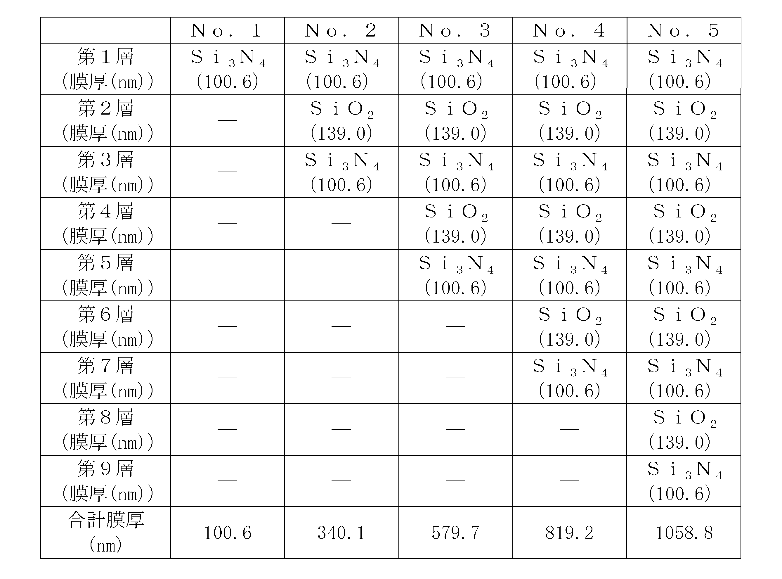
- a SiO 2 film (low refractive index layer) with a thickness of 139 nm and a Si 3 N 4 film (high with a thickness of 100.6 nm) are formed on the periphery of the element substrate 3 so as to straddle the electrodes 6 and 7.
- a total of nine layers are formed alternately with the refractive index layer), and the dielectric multilayer film 8 is formed.
- the dielectric multilayer film 8 is formed by alternately laminating low refractive index layers and high refractive index layers by, for example, CVD, sputtering, vacuum deposition, or the like.
- the element substrate 3 and the sealing substrate 4 are disposed to face each other, the glass frit 5 and the dielectric multilayer film 8 are brought into contact with each other, and then the glass frit 5 is irradiated with laser light from the sealing substrate 4 side. Then, the glass frit 5 is melted, and the glass frit 5 and the dielectric multilayer film 8 are directly welded. As a result, the entire outer periphery of the element substrate 3 and the sealing substrate 4 is joined, and the organic EL layer 2 is hermetically sealed.
- each dielectric layer constituting the dielectric multilayer film 8 can maintain better adhesion with the glass frit 5 than the metal layer. Therefore, in addition to the dielectric multilayer film 8, the adhesive force with the glass frit 5 can be favorably maintained without providing a new layer only in order to increase the adhesive force with the glass frit 5.
- each dielectric layer constituting the dielectric multilayer film 8 has no electrical conductivity, there is no electrical connection between the electrodes 6 and 7 connected to the organic EL layer 2 without providing an insulating layer separately. Insulation can be kept. Accordingly, it is not an essential condition to separately provide an improvement layer for improving the adhesive strength with the glass frit 5 or an insulating layer, so that the degree of freedom in designing the organic EL element package 1 can be ensured.
- the laser light emitted from the laser L can be obtained by adjusting the material selection and the film thickness of the low refractive index dielectric layer and the high refractive index dielectric layer. In this wavelength band, it is possible to easily realize an excellent reflectance. Therefore, when laser light is irradiated to the glass frit 5 from the sealing substrate 4 side during the welding of the glass frit 5, the laser light is reliably reflected to the glass frit 5 side by the dielectric multilayer film 8, and the glass frit 5 is heated. It is used effectively. Accordingly, the laser light that passes through the dielectric multilayer film 8 and is applied to the electrodes 6 and 7 is reduced as much as possible. Therefore, the electrodes 6 and 7 and the organic EL layer 2 are unduly heated by the laser light, It is possible to reliably prevent a situation in which heat damage occurs.
- the first invention is not limited to the above-described embodiment, and can be implemented in various forms.
- the case where the dielectric multilayer film 8 is formed directly on the electrodes 6 and 7 has been described, but an insulating layer may be interposed.
- an intermediate layer may be interposed between the dielectric multilayer film 8 and the glass frit 5.
- the first electrode 6 and the second electrode 7 are exemplified by a transparent electrode made of ITO or a metal electrode made of Al, but other transparent electrodes such as IZO, AZO, Ti, Ag, etc. Other metal electrodes such as Cu, Cr, and Mo may be used.
- the organic EL element package (organic EL display device) has been described as an example.
- the present invention is similarly applied to an electric element package used for other devices such as an organic EL lighting device and a solar battery. be able to.
- glass frits can be used in addition to the glass frit exemplified above. Specifically, for example, glass frit containing glass powder containing V 2 O 5 and ⁇ -eucryptite or zirconium tungstate phosphate, glass frit containing glass powder containing Bi 2 O 3 and cordierite or willemite is used. May be.
- FIG. 3 is a longitudinal sectional view showing a schematic configuration of the organic EL element package according to the present embodiment.
- the organic EL element package 1 includes an element substrate 3 on which an organic EL layer 2 is formed, a sealing substrate 4 facing the surface of the element substrate 3 on the organic EL layer 2 side with a space therebetween, and an organic EL layer 2.
- a glass frit 5 that hermetically seals the gap between the element substrate 3 and the sealing substrate 4 while surrounding the frame in a frame shape is provided as a basic configuration.
- the element substrate 3 and the sealing substrate 4 are made of, for example, a 0.05 to 2 mm glass substrate.
- the sealing substrate 4 may be formed with a certain thickness of digging.
- the element substrate 3 is provided with a first electrode 6 and a second electrode 7 connected to both the front and back sides of the organic EL layer 2.
- the electrodes 6 and 7 are guided from the organic EL layer 2 to the outside of the organic EL element package 1 through the lower part of the glass frit 5 to supply electric power to the organic EL layer 2.
- the electrodes 6 and 7 are branched according to a predetermined pattern as shown in FIG.
- the first electrode 6 on the back side of the organic EL layer 2 is formed of, for example, a transparent electrode film (ITO film), and the second electrode 7 on the front side of the organic EL layer is, for example, a metal electrode film such as aluminum. Formed with.
- Both the first electrode 6 and the second electrode 7 may be formed of a transparent electrode film.
- the laser light emitted from the laser L is irradiated onto the glass frit 5 from the sealing substrate 4 side, and the glass frit 5 is heated and softened to flow to seal the element substrate 3.
- the laser L for example, a near infrared semiconductor laser (wavelength 800 to 1100 nm) is used.
- the electrodes 6 and 7 may be thermally damaged.
- the heat is transmitted to the organic EL layer 2 through the electrodes 6 and 7, and the organic EL layer 2 may be thermally damaged. Therefore, in the present embodiment, the metal oxide film 9 functioning as a protective film is interposed between the glass frit 5 and the electrodes 6 and 7 to protect the electrodes 6 and 7 from laser light. .
- the metal oxide film 9 functioning as a protective layer is preferably one that has excellent adhesion to the glass frit 5 and the electrodes 6 and 7 and exhibits insulation properties. These materials, SiO 2, ZrO 2, Y 2 O 3, TiO 2, Al 2 O 3, Ta 2 O 5, and Nb 2 O 5 and the like.
- the film thickness of the metal oxide film 9 is preferably 5 to 500 nm, 10 to 300 nm, particularly 30 to 300 nm.
- the thickness of the metal oxide film 9 is smaller than 5 nm, the effect of protecting the electrodes 6 and 7 is reduced.
- it is larger than 500 nm, the amount of stress due to the difference in thermal expansion between the glass frit 5 and the metal oxide film 9 becomes large, and peeling between the glass frit 5 and the metal oxide film 9 tends to occur after laser welding. .
- the manufacturing cost of the electric element package increases.
- the glass frit 5 a glass frit containing 80 to 99.95% by mass of an inorganic powder containing SnO-containing glass powder and 0.05 to 20% by mass of a pigment is preferable.
- the content of the inorganic powder is preferably 90 to 99.95% by mass, 95 to 99.95% by mass, and particularly preferably 99 to 99.95% by mass.
- the content of the inorganic powder is small, the softening flow of the glass frit 5 becomes poor during laser welding, and it becomes difficult to increase the welding strength.
- the content of the inorganic powder is higher than 99.95% by mass, the content of the pigment is relatively decreased, and thus the laser beam absorption performance of the glass frit 5 is lowered.
- the glass frit easily absorbs laser light, so that the efficiency of laser welding is improved and it is easy to prevent thermal damage to electrodes and electric elements. .
- the pigment content is restricted to 20% by mass or less, it is easy to prevent the glass frit from devitrifying during laser welding.
- the average particle diameter D 50 of SnO-containing glass powder, the maximum particle diameter D max , and preferred embodiments of the glass composition are the same as described above, and detailed description thereof is omitted for convenience.
- the softening point of the SnO-containing glass powder is preferably the same as described above.
- the pigment is preferably an inorganic pigment, one or two selected from carbon, Co 3 O 4 , CuO, Cr 2 O 3 , Fe 2 O 3 , MnO 2 , SnO, and Ti n O 2n-1 (n is an integer).
- carbon is particularly preferable.
- carbon amorphous carbon and griffite are preferable. These pigments have excellent color developability and good laser light absorption performance.
- the average particle diameter D 50 of the pigment, the average particle diameter D 50 of the primary particles of the pigment is preferably in the same manner as described above. And it is preferable that a pigment does not contain Cr type oxide substantially from an environmental viewpoint.
- the glass frit 5 preferably further contains a refractory filler. In this way, the thermal expansion coefficient of the glass frit 5 can be reduced, and the mechanical strength of the glass frit 5 can be increased.
- the mixing ratio of the SnO-containing glass powder and the refractory filler in the inorganic powder is preferably adjusted in the same manner as described above.
- a preferred embodiment of the material of the refractory filler and the maximum particle diameter Dmax is the same as described above.
- the preferable range of the thermal expansion coefficient of the glass frit 5 is the same as described above.
- the glass frit 5 is preferably used after being kneaded with a vehicle and processed into a paste material. If it does in this way, workability
- the vehicle usually includes a resin binder and a solvent.
- the resin binder and the solvent are preferably the same as described above, and detailed description thereof is omitted for convenience.
- laser welding is preferably performed in an inert atmosphere, particularly preferably in an N 2 atmosphere. If it does in this way, it will become easy to prevent the situation which SnO containing glass powder changes in the case of laser welding.
- a paste-like glass frit 5 is applied to the peripheral edge of the sealing substrate 4 with, for example, a screen printer with a thickness of about 40 ⁇ m and a width of about 0.6 mm, and then dried and baked to obtain a paste.
- the glass frit is softened and fluidized to firmly adhere to the sealing substrate 4.
- the height of the glass frit 5 after firing is, for example, about 15 ⁇ m.
- the first electrode 6 is formed in a predetermined pattern with a thickness of 150 nm, for example, SiO 2 with a thickness of 100 nm, for example, is formed in a region facing the peripheral portion where the glass frit 5 is printed and fired.
- Two films 9 are formed.
- the SiO 2 film 9 is formed by, for example, a CVD method, a sputtering method, a vacuum vapor deposition method, or the like.
- the organic EL layer 2 is formed, and the second electrode 7 is formed thereon with a predetermined pattern.
- the element substrate 3 and the sealing substrate 4 are arranged to face each other, the glass frit 5 and the SiO 2 film 9 are brought into contact with each other, and then the glass frit 5 is irradiated with laser light from the sealing substrate 4 side. Then, the glass frit 5 is melted and softened and fluidized to directly weld the glass frit 5 and the SiO 2 film 9. Thereby, the element substrate 3 and the sealing substrate 4 are joined along the outer periphery, and the organic EL layer 2 is hermetically sealed.
- 2nd invention is not limited to said embodiment, It can implement with a various form.
- the SiO 2 film 9 is formed on the first electrode 6 has been described in the above embodiment, it may be formed on the glass frit 5 on the sealing substrate 4 side.
- the first electrode 6 and the second electrode 7 are exemplified by a transparent electrode made of ITO or a metal electrode made of Al, but other transparent electrodes such as IZO, AZO, FTO and ZnO, , Ti, Ag, Cu, Cr, Mo and other metal electrodes such as multilayer films thereof may be used.
- the organic EL element package (organic EL display device) has been described as an example, but the present invention is similarly applied to an electric element package used for other devices such as an organic EL lighting device and a solar battery. be able to.
- glass frits can be used in addition to the glass frit exemplified above. Specifically, for example, glass frit containing glass powder containing V 2 O 5 and ⁇ -eucryptite, glass frit containing glass powder containing Bi 2 O 3 and cordierite or willemite may be used.
- the first invention will be described in detail based on examples.
- the first invention is not limited to the following examples.
- the following examples are merely illustrative.
- Table 1 shows the design values of the film configurations of Examples (No. 2 to No. 4) of the dielectric multilayer film used in the electrical element package according to the first invention.
- Table 1 a single-layer dielectric film is shown as a comparative example (No. 1).
- the dielectric multilayer film having a film structure as shown in Table 1 shows the wavelength characteristic of reflectance as shown in FIG.
- the wavelength characteristic of the reflectance is improved as the number of layers is increased as compared with the three-layered example (No. 2), and the nine-layered example (No. 5).
- the maximum reflectivity reaches about 90%.
- the reflectance with respect to infrared laser light having a wavelength of 808 nm is maximized.
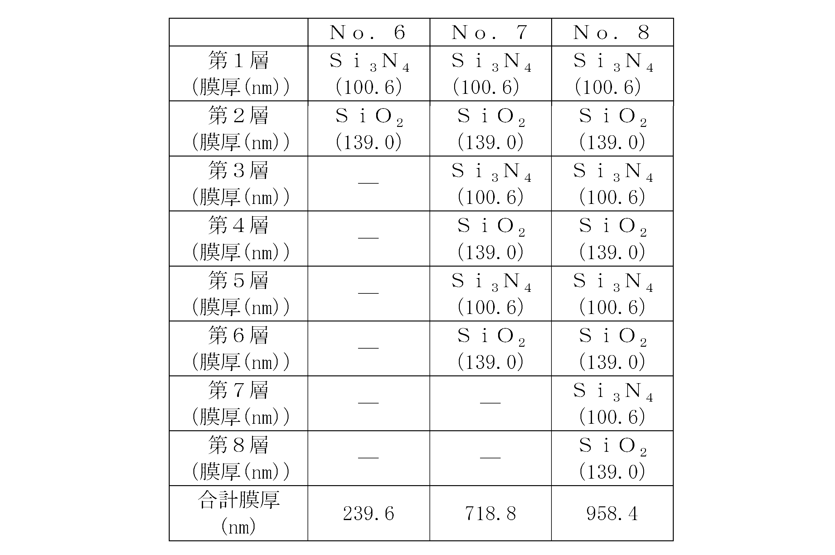
- Table 2 shows examples of film configurations of Examples (No. 6 to No. 8) of dielectric multilayer films used in the electrical element package according to the first invention.
- the frequency characteristics of the reflectance in this example are as shown in FIG.
- the reflectance is maximum near the wavelength of 808 nm, and the example consisting of 8 layers (No. 8). Then, the maximum reflectance of about 70% is realized.
- a paste-like glass frit is printed on the peripheral edge of a glass substrate having a length of 40 mm, a width of 50 mm, and a thickness of 0.5 mm by screen printing to a thickness of 15 ⁇ m, followed by temporary firing at 500 ° C. for 1 hour, Once cured, a sealing substrate was produced.
- the glass frit one containing 99% by mass of inorganic powder and 1% by mass of pigment was used.
- the inorganic powder contained in the glass frit contains 60% by volume of SnO glass powder and 40% by volume of refractory filler.
- SnO-based glass powder contains SnO 59%, P 2 O 5 20%, ZnO 5%, B 2 O 3 15%, and Al 2 O 3 1% in terms of glass composition.
- the glass powder has an average particle diameter D 50 of 2.5 [mu] m, maximum particle diameter D max is 7 [mu] m.
- Refractory filler consists zirconium phosphate powder, the average particle diameter D 50 of 2 [mu] m, maximum particle diameter D max is 8 [mu] m.
- the pigment contained in the glass frit consists of carbon powder, the average particle diameter D 50 of 0.5 [mu] m, maximum particle diameter D max is 3 [mu] m.
- a first electrode made of ITO is formed to a thickness of 150 nm on a glass substrate having a length of 40 mm, a width of 50 mm, and a thickness of 0.5 mm.
- a first electrode made of an organic EL layer and Al is formed on the glass substrate. Two electrodes were respectively formed by vacuum deposition to produce an element substrate.
- a laser beam having a wavelength of 808 nm is irradiated from the sealing substrate side to weld a glass frit to perform hermetic sealing.
- the laser beam irradiation was performed while moving the laser beam with an output of 20 W to the periphery of the glass substrate at 5 mm / s.
- thermometer The temperature measurement during the laser welding was first performed on the first electrode made of ITO.
- temperature measurement (1) As a comparative example, a dielectric multilayer film is not disposed on the first electrode (No. 9), (2) As an example, a two-layer dielectric multilayer film having the same configuration as the above example (No. 6) is arranged on the first electrode (No. 10), and (3) the first An eight-layer dielectric multilayer film having the same configuration as that of the above-described embodiment (No. 8) is disposed on the electrode (No. 11). Went against. The result is shown in FIG.
- the temperature of the first electrode (ITO) of the comparative example (No. 9) in which the dielectric multilayer film is not disposed exceeds 400 ° C., whereas the dielectric multilayer film is disposed.
- the temperatures of the first electrodes in the examples (No. 10 to No. 11) are lower than 400 ° C.
- the temperature of the second electrode is lowered to about 220 ° C., which is sufficient for preventing thermal damage of the first electrode. Can be recognized.
- temperature measurement at the time of laser welding was performed on the second electrode made of Al.
- temperature measurement (1) As a comparative example, a dielectric multilayer film is not disposed on the second electrode (No. 12), (2) As an example, a two-layer dielectric multilayer film having the same configuration as the above example (No. 6) is disposed on the second electrode (No. 13), (3) A six-layer dielectric multilayer film having the same structure as that of the above-described embodiment (No. 7) is arranged on the second electrode (No. 14), and (4) on the second electrode.
- the test was carried out on an arrangement (No. 15) in which an eight-layer dielectric multilayer film having the same configuration as that of the above-mentioned Example (No. 8) was arranged. The result is shown in FIG.
- the temperature of the second electrode (Al) of the comparative example (No. 12) in which the dielectric multilayer film is not disposed rises to about 700 ° C.
- the dielectric multilayer film The temperature of the second electrode in Examples (Nos. 13 to 15) in which is arranged is lower than this.
- the temperature of the second electrode is up to about 150 ° C. Since it is lowered, it can be recognized that there is a sufficient effect in preventing thermal damage of the second electrode.
- the electrode material is ITO, (1) As a comparative example, a dielectric multilayer film is not disposed on the electrode (No. 16), (2) As an example, a two-layer dielectric multilayer film having the same configuration as the above example (No. 6) is disposed on the electrode (No. 17), (3) An electrode was inspected on an electrode (No. 18) in which an eight-layer dielectric multilayer film having the same configuration as that of the above-described Example (No.
- the examples in which the dielectric multilayer film is provided on the electrode (No. 17 to No. .18) has a higher frit glass temperature.
- the laser light is reflected to the frit glass side by the dielectric multilayer film, and the laser light is effectively used for heating the frit glass. Can be recognized.
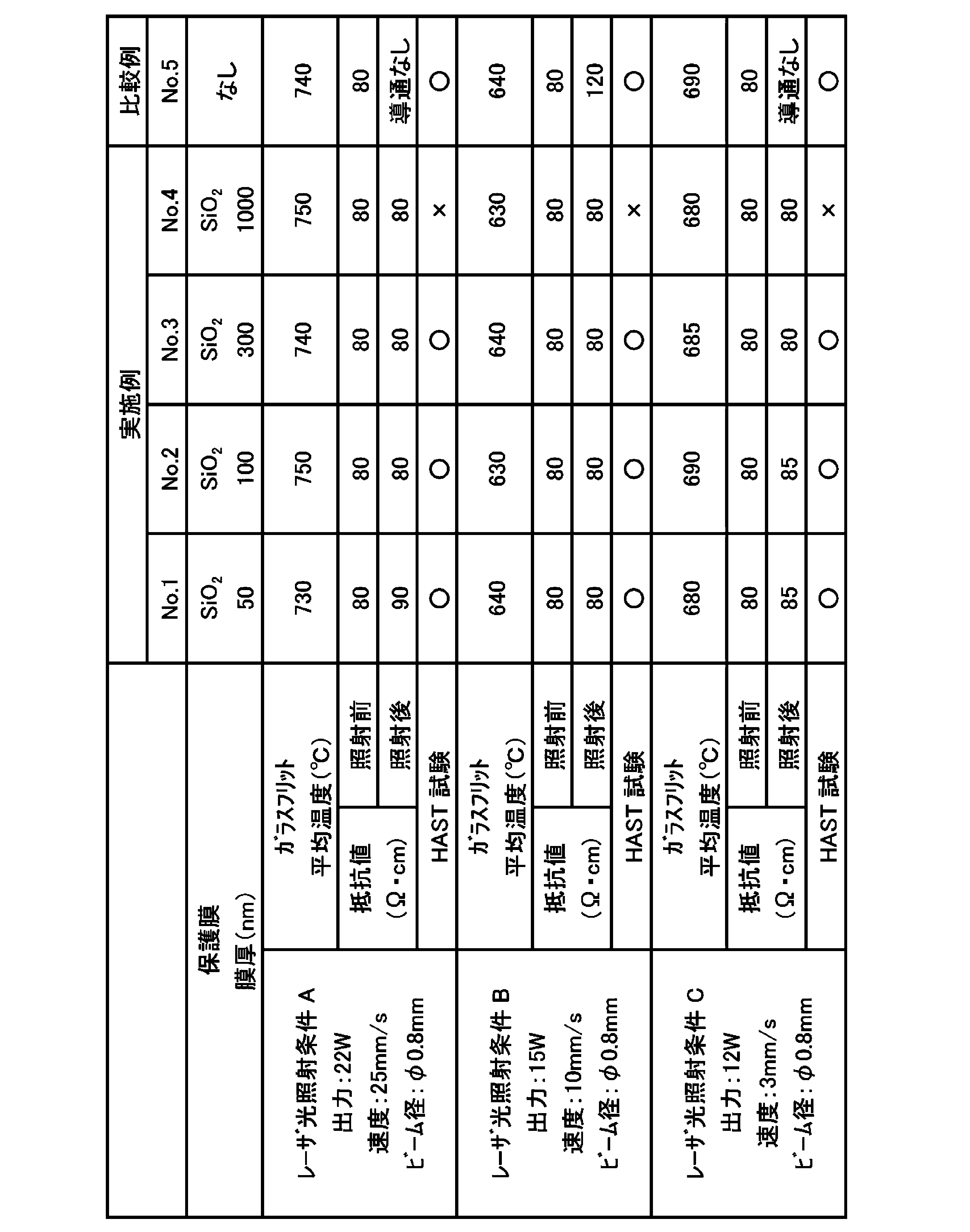
- Table 4 shows examples of the second invention (sample Nos. 1 to 4) and comparative examples (sample No. 5).
- the glass frit and the vehicle were kneaded so that the viscosity was about 150 Pa ⁇ s (25 ° C., Shear rate: 4), and then kneaded with a three-roll mill until uniform, to obtain a paste.
- a glass frit containing 99.75% by mass of inorganic powder and 0.25% by mass of pigment was used.
- the inorganic powder contained in the glass frit includes 60% by volume of SnO-based glass powder and 40% by volume of refractory filler.
- the SnO-based glass powder has a glass composition of mol%, SnO 59%, P 2 O 5.
- a material containing 20%, ZnO 5%, B 2 O 3 15%, Al 2 O 3 1% was used.
- the average particle diameter D 50 of the glass powder is 2 [mu] m, maximum particle diameter D max was 5 [mu] m.
- the refractory filler was made of zirconium phosphate powder, the average particle diameter D 50 was 1.5 ⁇ m, and the maximum particle diameter D max was 3.5 ⁇ m.
- Pigment contained in the glass frit consists of carbon powder, the average particle diameter D 50 of the primary particles were from about 30 nm.
- Polyethylene carbonate resin (MW: 129000) was used as the resin component of the vehicle, and propylene carbonate was used as the solvent component.
- the softening point of the glass frit was 400 ° C., and the thermal expansion coefficient of the glass frit was 49 ⁇ 10 ⁇ 7 / ° C. (measurement temperature range: 30 to 300 ° C.).
- the softening point is a value measured with a DTA apparatus
- the thermal expansion coefficient is a value measured with a TMA apparatus.
- a paste-like glass frit adjusted as described above was applied to the peripheral edge of a glass substrate (40 mm long ⁇ 50 mm wide ⁇ 0.5 mm thick) (OA-10G manufactured by Nippon Electric Glass Co., Ltd.) by screen printing to obtain a thickness of about: After printing to 30 ⁇ m and width: about 0.6 mm, it is dried in air atmosphere at 120 ° C. for 30 minutes, and baked in nitrogen atmosphere at 480 ° C. for 10 minutes. The resin component in the paste was decomposed and volatilized, and the glass frit was fixed to the glass substrate to produce a sealing substrate. The thickness of the glass frit after firing was about 16 ⁇ m. When the surface roughness of the glass frit after firing was measured, the Ra value was 0.5 ⁇ m and the RMS value was 0.8 ⁇ m.
- a glass frit is formed.
- a SiO 2 film was formed to a thickness of 50, 100, 300, or 1000 nm within the range to be fixed.
- a SiO 2 film having a width of about 1 mm was formed so that the glass frit and the ITO film were not in contact with each other.
- an organic EL layer and a second electrode made of Al were formed on the glass substrate by a vacuum vapor deposition method, thereby producing an element substrate.
- laser light having a wavelength of 808 nm was irradiated along the glass frit from the sealing substrate side to weld the sealing substrate and the element substrate. .
- the laser light irradiation conditions are as described in the table.
- the temperature of the glass frit at the time of laser light irradiation was measured.
- the electrical resistance of the ITO film directly under the glass frit was measured to evaluate the presence or absence of thermal degradation of the ITO film.
- HAST test Highly Accelerated Temperature and Humidity Stress Test
- x The conditions of the HAST test were 121 ° C., 100% RH, 2 atm, and 24 hours.
- sample No. In No. 5 since the SiO 2 film was not formed, the resistance value of the ITO film increased after laser light irradiation. In particular, under the laser light irradiation conditions A and C, the ITO film was severely thermally damaged, and thus the resistance value of the ITO film could not be measured.
Landscapes
- Chemical & Material Sciences (AREA)
- Engineering & Computer Science (AREA)
- Geochemistry & Mineralogy (AREA)
- Life Sciences & Earth Sciences (AREA)
- Chemical Kinetics & Catalysis (AREA)
- General Chemical & Material Sciences (AREA)
- Materials Engineering (AREA)
- Organic Chemistry (AREA)
- Optics & Photonics (AREA)
- Physics & Mathematics (AREA)
- Mechanical Engineering (AREA)
- Inorganic Chemistry (AREA)
- Glass Compositions (AREA)
- Electroluminescent Light Sources (AREA)
Abstract
Description
A:Li、Na、K、Mg、Ca、Sr、Ba、Zn、Cu、Ni、Mn等
B:Zr、Ti、Sn、Nb、Al、Sc、Y等
M:P、Si、W、Mo等
若しくはこれらの固溶体が使用可能である。
第一の発明に係る電気素子パッケージに使用する誘電体多層膜の実施例(No.2~No.4)の膜構成の設計値を表1に示す。なお、表1において、比較例(No.1)として単層の誘電体膜を示す。
第一の発明に係る電気素子パッケージに使用する誘電体多層膜の実施例(No.6~No.8)の膜構成の実例を表2に示す。
縦40mm×横50mm×厚み0.5mmのガラス基板の周縁部にペースト状のガラスフリットをスクリーン印刷により15μmの厚みで印刷した後、500℃で1時間に亘って仮焼成を行い、ガラスフリットを一旦硬化させ、封止基板を製作した。
(1)比較例として第1電極の上に誘電体多層膜を配置していないもの(No.9)、
(2)実施例として第1電極の上に上記の実施例(No.6)と同様の構成の2層の誘電体多層膜を配置したもの(No.10)、および、(3)第1電極の上に上記の実施例(No.8)と同様の構成の8層の誘電体多層膜を配置したもの(No.11)
に対して行った。その結果を図7に示す。
(1)比較例として第2電極の上に誘電体多層膜を配置していないもの(No.12)、
(2)実施例として第2電極の上に上記の実施例(No.6)と同様の構成の2層の誘電体多層膜を配置したもの(No.13)、
(3)第2電極の上に上記の実施例(No.7)と同様の構成の6層の誘電体多層膜を配置したもの(No.14)、および
(4)第2電極の上に上記の実施例(No.8)と同様の構成の8層の誘電体多層膜を配置したもの(No.15)に対して行った。その結果を図8に示す。
レーザ溶着時に、出力12Wのレーザ光をガラス基板の周縁に、3mm/sで移動させながら照射し、ガラスフリットを溶融させ、このときの電極の熱損傷の有無を検査した。詳細には、電極材料はITOとし、
(1)比較例として電極の上に誘電体多層膜を配置していないもの(No.16)、
(2)実施例として電極の上に上記の実施例(No.6)と同様の構成の2層の誘電体多層膜を配置したもの(No.17)、
(3)電極の上に上記の実施例(No.8)と同様の構成の8層の誘電体多層膜を配置したもの(No.18)に対して、電極の検査を行った。なお、電極が熱損傷を来たしているか否かの判断は、導通の有無で判断した。すなわち、電極が導通状態を維持している場合を熱損傷「なし」と、電極が非導通状態である場合を熱損傷「あり」とした。これは、電極が熱損傷を来たせば、線路の途中で断線するためである。その結果を表3に示す。

2 有機EL層
3 素子基板
4 封止基板
5 ガラスフリット
6 第1電極
7 第2電極
8 誘電体多層膜
9 金属酸化物膜(SiO2膜)
L レーザ
Claims (15)
- 電気素子が配置された素子基板と、該素子基板の前記電気素子側の表面に間隔を置いて対向する封止基板と、前記電気素子の周囲を囲むように前記素子基板と前記封止基板との間の隙間を気密封止するガラスフリットを有する電子素子パッケージにおいて、
前記素子基板と前記ガラスフリットの間に配置され、且つ前記ガラスフリットを溶着する際に照射されるレーザ光から電極を保護するための保護膜を有することを特徴とする電気素子パッケージ。 - 電気素子が配置された素子基板と、該素子基板の前記電気素子側の表面に間隔を置いて対向する封止基板と、前記電気素子の周囲を囲むように前記素子基板と前記封止基板との間の隙間を気密封止するガラスフリットを有する電子素子パッケージにおいて、
前記素子基板と前記ガラスフリットの間に配置され、前記ガラスフリットを溶着する際に照射されるレーザ光を反射する反射膜を有し、
前記反射膜が、低屈折率誘電体層と、高屈折率誘電体層とを交互に積層した誘電体多層膜からなることを特徴とする電気素子パッケージ。 - 前記誘電体多層膜が、前記ガラスフリットに直接溶着されていることを特徴とする請求項2に記載の電気素子パッケージ。
- 前記誘電体多層膜が、前記電気素子に接続された電極の上に直接形成されていることを特徴とする請求項2又は3に記載の電気素子パッケージ。
- 前記低屈折率誘電体層の屈折率が、1.6以下であって、前記高屈折率誘電体層の屈折率が、1.7以上であることを特徴とする請求項2~4のいずれか1項に記載の電気素子パッケージ。
- 前記誘電体多層膜が、前記レーザ光に対する反射率が50%以上であることを特徴とする請求項2~5のいずれか1項に記載の電気素子パッケージ。
- 前記ガラスフリットが、SnO含有ガラス粉末を含む無機粉末 80~99.7質量%と、顔料 0.3~20質量%とを含有することを特徴とする請求項2~6のいずれか1項に記載の電気素子パッケージ。
- 前記SnO含有ガラス粉末が、ガラス組成として、モル%で、SnO 35~70%、P2O5 10~30%を含有することを特徴とする請求項7に記載の電気素子パッケージ。
- 電気素子が配置された素子基板と、該素子基板の前記電気素子側の表面に間隔を置いて対向する封止基板と、前記電気素子の周囲を囲むように前記素子基板と前記封止基板との間の隙間を気密封止するガラスフリットを有する電気素子パッケージにおいて、
前記素子基板と前記ガラスフリットの間に配置され、且つ前記ガラスフリットを溶着する際に照射されるレーザ光から電極を保護するための金属酸化物膜を有することを特徴とする電気素子パッケージ。 - 前記金属酸化物膜の厚みが10~500nmであることを特徴とする請求項9に記載の電気素子パッケージ。
- 前記金属酸化物膜が、SiO2、ZrO2、Y2O3、TiO2、Al2O3、Ta2O5、Nb2O5のいずれかであることを特徴とする請求項9又は10に記載の電気素子パッケージ。
- 前記金属酸化物膜が、前記ガラスフリットに直接溶着されていることを特徴とする請求項9~11のいずれか1項に記載の電気素子パッケージ。
- 前記金属酸化物膜が、前記電気素子に接続された電極の上に直接形成されていることを特徴とする請求項9~12のいずれかに記載の電気素子パッケージ。
- 前記ガラスフリットが、SnO含有ガラス粉末を含む無機粉末 80~99.95質量%と、顔料 0.05~20質量%とを含有することを特徴とする請求項9~13のいずれか1項に記載の電気素子パッケージ。
- 前記SnO含有ガラス粉末が、ガラス組成として、モル%で、SnO 35~70%、P2O5 10~30%を含有することを特徴とする請求項14に記載の電気素子パッケージ。
Priority Applications (3)
| Application Number | Priority Date | Filing Date | Title |
|---|---|---|---|
| KR1020127027084A KR20130119319A (ko) | 2010-10-01 | 2011-09-30 | 전기소자 패키지 |
| US13/876,662 US20130213852A1 (en) | 2010-10-01 | 2011-09-30 | Electrical element package |
| CN2011800240885A CN102893700A (zh) | 2010-10-01 | 2011-09-30 | 电气元件封装体 |
Applications Claiming Priority (4)
| Application Number | Priority Date | Filing Date | Title |
|---|---|---|---|
| JP2010-223888 | 2010-10-01 | ||
| JP2010223888A JP2012079550A (ja) | 2010-10-01 | 2010-10-01 | 電気素子パッケージ |
| JP2010261986A JP2012113968A (ja) | 2010-11-25 | 2010-11-25 | 電気素子パッケージ |
| JP2010-261986 | 2010-11-25 |
Publications (1)
| Publication Number | Publication Date |
|---|---|
| WO2012043787A1 true WO2012043787A1 (ja) | 2012-04-05 |
Family
ID=45893224
Family Applications (1)
| Application Number | Title | Priority Date | Filing Date |
|---|---|---|---|
| PCT/JP2011/072527 Ceased WO2012043787A1 (ja) | 2010-10-01 | 2011-09-30 | 電気素子パッケージ |
Country Status (5)
| Country | Link |
|---|---|
| US (1) | US20130213852A1 (ja) |
| KR (1) | KR20130119319A (ja) |
| CN (1) | CN102893700A (ja) |
| TW (1) | TW201216458A (ja) |
| WO (1) | WO2012043787A1 (ja) |
Cited By (1)
| Publication number | Priority date | Publication date | Assignee | Title |
|---|---|---|---|---|
| JP2024023685A (ja) * | 2011-11-28 | 2024-02-21 | 株式会社半導体エネルギー研究所 | 発光装置及び発光モジュール |
Families Citing this family (25)
| Publication number | Priority date | Publication date | Assignee | Title |
|---|---|---|---|---|
| KR102038844B1 (ko) * | 2011-06-16 | 2019-10-31 | 가부시키가이샤 한도오따이 에네루기 켄큐쇼 | 밀봉체의 제작 방법 및 밀봉체, 그리고 발광 장치의 제작 방법 및 발광 장치 |
| KR20140016170A (ko) | 2012-07-30 | 2014-02-07 | 가부시키가이샤 한도오따이 에네루기 켄큐쇼 | 밀봉체 및 유기 전계 발광 장치 |
| CN103219474B (zh) * | 2013-03-25 | 2016-03-23 | 京东方科技集团股份有限公司 | 一种基板封装方法 |
| KR102072805B1 (ko) * | 2013-04-15 | 2020-02-04 | 삼성디스플레이 주식회사 | 유기발광표시장치 및 그의 제조방법 |
| CN103500799B (zh) * | 2013-09-24 | 2015-10-14 | 京东方科技集团股份有限公司 | 一种oled器件的封装结构和封装方法 |
| CN104716266B (zh) * | 2013-12-13 | 2017-10-17 | 昆山国显光电有限公司 | 一种窄边框有机发光显示器 |
| KR102205356B1 (ko) * | 2014-01-29 | 2021-01-21 | 삼성디스플레이 주식회사 | 표시 패널 및 이의 제조 방법 |
| EP3111490A1 (en) * | 2014-02-28 | 2017-01-04 | Corning Incorporated | Flexible display device packages and methods of manufacturing |
| CN104091900B (zh) * | 2014-05-20 | 2016-08-17 | 四川虹视显示技术有限公司 | 一种oled线阵式激光封装装置 |
| US20150372251A1 (en) * | 2014-06-19 | 2015-12-24 | Toshishige Fujii | Electric element package |
| TWI686968B (zh) * | 2015-02-26 | 2020-03-01 | 日商日本電氣硝子股份有限公司 | 氣密封裝及其製造方法 |
| JP2018537395A (ja) * | 2015-11-24 | 2018-12-20 | コーニング インコーポレイテッド | 粒子膜開始薄肉レーザ溶接部を有する封止デバイスハウジングおよび関連の方法 |
| CN105448956B (zh) * | 2015-12-30 | 2019-01-25 | 昆山国显光电有限公司 | 一种有机发光显示装置及其制备方法 |
| KR20170079877A (ko) * | 2015-12-31 | 2017-07-10 | 주식회사 동진쎄미켐 | 접착필름의 봉지 기술을 이용한 유기전자소자 및 이의 제조 방법 |
| US10531555B1 (en) * | 2016-03-22 | 2020-01-07 | The United States Of America As Represented By The Secretary Of The Army | Tungsten oxide thermal shield |
| CN105739154B (zh) * | 2016-04-29 | 2019-09-27 | 上海天马有机发光显示技术有限公司 | 一种显示面板以及电子设备 |
| JP6913276B2 (ja) * | 2017-01-26 | 2021-08-04 | 日本電気硝子株式会社 | 気密パッケージ |
| CN109390352A (zh) | 2017-08-09 | 2019-02-26 | 昆山国显光电有限公司 | 阵列基板及其制造方法、显示面板及其制造方法 |
| CN107591495B (zh) * | 2017-08-18 | 2019-06-25 | 武汉华星光电半导体显示技术有限公司 | 熔接金属板及显示装置 |
| JP7168903B2 (ja) * | 2018-09-06 | 2022-11-10 | 日本電気硝子株式会社 | 気密パッケージ |
| WO2021166568A1 (ja) * | 2020-02-18 | 2021-08-26 | 日本電気硝子株式会社 | ガラス組成物及び封着材料 |
| WO2021199613A1 (ja) * | 2020-03-31 | 2021-10-07 | 日本電気硝子株式会社 | 接合体の製造方法及び接合体 |
| CN111477705B (zh) * | 2020-04-15 | 2022-03-18 | 中国科学院电工研究所 | 一种去除晶硅光伏组件背面有机粘结胶膜的方法 |
| US11086170B1 (en) * | 2020-05-20 | 2021-08-10 | Himax Display, Inc. | Display device |
| JP7616507B2 (ja) * | 2020-09-09 | 2025-01-17 | 日本電気硝子株式会社 | ガラス組成物及び封着材料 |
Citations (4)
| Publication number | Priority date | Publication date | Assignee | Title |
|---|---|---|---|---|
| JP2007200883A (ja) * | 2006-01-23 | 2007-08-09 | Samsung Sdi Co Ltd | 有機電界発光表示装置及びその製造方法 |
| WO2008007504A1 (fr) * | 2006-07-11 | 2008-01-17 | Nippon Electric Glass Co., Ltd. | Composition de verre pour l'étanchéité et matériau étanche |
| JP2008288376A (ja) * | 2007-05-17 | 2008-11-27 | Toshiba Matsushita Display Technology Co Ltd | 表示装置および表示装置の製造方法 |
| JP2009076437A (ja) * | 2007-08-31 | 2009-04-09 | Toshiba Matsushita Display Technology Co Ltd | 表示装置 |
Family Cites Families (2)
| Publication number | Priority date | Publication date | Assignee | Title |
|---|---|---|---|---|
| KR100685852B1 (ko) * | 2006-01-23 | 2007-02-22 | 삼성에스디아이 주식회사 | 유기전계발광표시장치 및 그 제조방법 |
| US20090058293A1 (en) * | 2007-08-31 | 2009-03-05 | Norihisa Maeda | Display device |
-
2011
- 2011-09-30 CN CN2011800240885A patent/CN102893700A/zh active Pending
- 2011-09-30 KR KR1020127027084A patent/KR20130119319A/ko not_active Withdrawn
- 2011-09-30 TW TW100135621A patent/TW201216458A/zh unknown
- 2011-09-30 US US13/876,662 patent/US20130213852A1/en not_active Abandoned
- 2011-09-30 WO PCT/JP2011/072527 patent/WO2012043787A1/ja not_active Ceased
Patent Citations (4)
| Publication number | Priority date | Publication date | Assignee | Title |
|---|---|---|---|---|
| JP2007200883A (ja) * | 2006-01-23 | 2007-08-09 | Samsung Sdi Co Ltd | 有機電界発光表示装置及びその製造方法 |
| WO2008007504A1 (fr) * | 2006-07-11 | 2008-01-17 | Nippon Electric Glass Co., Ltd. | Composition de verre pour l'étanchéité et matériau étanche |
| JP2008288376A (ja) * | 2007-05-17 | 2008-11-27 | Toshiba Matsushita Display Technology Co Ltd | 表示装置および表示装置の製造方法 |
| JP2009076437A (ja) * | 2007-08-31 | 2009-04-09 | Toshiba Matsushita Display Technology Co Ltd | 表示装置 |
Cited By (2)
| Publication number | Priority date | Publication date | Assignee | Title |
|---|---|---|---|---|
| JP2024023685A (ja) * | 2011-11-28 | 2024-02-21 | 株式会社半導体エネルギー研究所 | 発光装置及び発光モジュール |
| JP7581471B2 (ja) | 2011-11-28 | 2024-11-12 | 株式会社半導体エネルギー研究所 | 発光装置及び発光モジュール |
Also Published As
| Publication number | Publication date |
|---|---|
| TW201216458A (en) | 2012-04-16 |
| KR20130119319A (ko) | 2013-10-31 |
| CN102893700A (zh) | 2013-01-23 |
| US20130213852A1 (en) | 2013-08-22 |
Similar Documents
| Publication | Publication Date | Title |
|---|---|---|
| WO2012043787A1 (ja) | 電気素子パッケージ | |
| JP2012079550A (ja) | 電気素子パッケージ | |
| US10026923B2 (en) | Electronic component, method for producing same, and sealing material paste used in same | |
| CN102471151B (zh) | 带密封材料层的玻璃构件以及使用该构件的电子器件及其制造方法 | |
| CN102245525B (zh) | 密封玻璃、带密封材料层的玻璃构件以及电子器件及其制造方法 | |
| CN102792413B (zh) | 电子器件及其制造方法 | |
| CN102172101B (zh) | 电子器件用基板及其制造方法、使用该基板的电子器件及其制造方法以及有机led元件用基板 | |
| US20150380330A1 (en) | Package substrate, package, and electronic device | |
| CN103328402B (zh) | 带封接材料层的玻璃构件和使用其的电子装置及其制造方法 | |
| US20140023803A1 (en) | Airtight member and its production process | |
| CN102224115A (zh) | 带密封材料层的玻璃构件以及使用该构件的电子器件及其制造方法 | |
| JP2012113968A (ja) | 電気素子パッケージ | |
| JP2013239609A (ja) | 気密部材とその製造方法 | |
| JP2024041707A (ja) | 封着材料層付きガラス基板及び気密パッケージの製造方法 | |
| WO2010137667A1 (ja) | 封着材料層付きガラス部材とそれを用いた電子デバイスおよびその製造方法 | |
| CN108883971A (zh) | 玻璃粉末及使用其的密封材料 | |
| WO2012077771A1 (ja) | 反射鏡およびその製造方法 | |
| JP6090703B2 (ja) | 複合封着材料 | |
| JP2012121110A (ja) | Mems素子パッケージ | |
| JPWO2018216587A1 (ja) | 気密パッケージの製造方法及び気密パッケージ | |
| CN110268516A (zh) | 封装件基体以及使用了该封装件基体的气密封装件 | |
| WO2012046817A1 (ja) | 電子デバイス及びその製造方法 |
Legal Events
| Date | Code | Title | Description |
|---|---|---|---|
| WWE | Wipo information: entry into national phase |
Ref document number: 201180024088.5 Country of ref document: CN |
|
| 121 | Ep: the epo has been informed by wipo that ep was designated in this application |
Ref document number: 11829340 Country of ref document: EP Kind code of ref document: A1 |
|
| ENP | Entry into the national phase |
Ref document number: 20127027084 Country of ref document: KR Kind code of ref document: A |
|
| NENP | Non-entry into the national phase |
Ref country code: DE |
|
| WWE | Wipo information: entry into national phase |
Ref document number: 13876662 Country of ref document: US |
|
| 122 | Ep: pct application non-entry in european phase |
Ref document number: 11829340 Country of ref document: EP Kind code of ref document: A1 |