WO2012043508A1 - 太陽電池及びその製造方法 - Google Patents
太陽電池及びその製造方法 Download PDFInfo
- Publication number
- WO2012043508A1 WO2012043508A1 PCT/JP2011/071953 JP2011071953W WO2012043508A1 WO 2012043508 A1 WO2012043508 A1 WO 2012043508A1 JP 2011071953 W JP2011071953 W JP 2011071953W WO 2012043508 A1 WO2012043508 A1 WO 2012043508A1
- Authority
- WO
- WIPO (PCT)
- Prior art keywords
- solar cell
- semiconductor substrate
- electrode
- edge
- mark
- Prior art date
- Legal status (The legal status is an assumption and is not a legal conclusion. Google has not performed a legal analysis and makes no representation as to the accuracy of the status listed.)
- Ceased
Links
Images

Classifications
-
- H—ELECTRICITY
- H10—SEMICONDUCTOR DEVICES; ELECTRIC SOLID-STATE DEVICES NOT OTHERWISE PROVIDED FOR
- H10F—INORGANIC SEMICONDUCTOR DEVICES SENSITIVE TO INFRARED RADIATION, LIGHT, ELECTROMAGNETIC RADIATION OF SHORTER WAVELENGTH OR CORPUSCULAR RADIATION
- H10F10/00—Individual photovoltaic cells, e.g. solar cells
- H10F10/10—Individual photovoltaic cells, e.g. solar cells having potential barriers
- H10F10/14—Photovoltaic cells having only PN homojunction potential barriers
- H10F10/146—Back-junction photovoltaic cells, e.g. having interdigitated base-emitter regions on the back side
-
- H—ELECTRICITY
- H10—SEMICONDUCTOR DEVICES; ELECTRIC SOLID-STATE DEVICES NOT OTHERWISE PROVIDED FOR
- H10F—INORGANIC SEMICONDUCTOR DEVICES SENSITIVE TO INFRARED RADIATION, LIGHT, ELECTROMAGNETIC RADIATION OF SHORTER WAVELENGTH OR CORPUSCULAR RADIATION
- H10F77/00—Constructional details of devices covered by this subclass
- H10F77/20—Electrodes
- H10F77/206—Electrodes for devices having potential barriers
- H10F77/211—Electrodes for devices having potential barriers for photovoltaic cells
- H10F77/219—Arrangements for electrodes of back-contact photovoltaic cells
-
- Y—GENERAL TAGGING OF NEW TECHNOLOGICAL DEVELOPMENTS; GENERAL TAGGING OF CROSS-SECTIONAL TECHNOLOGIES SPANNING OVER SEVERAL SECTIONS OF THE IPC; TECHNICAL SUBJECTS COVERED BY FORMER USPC CROSS-REFERENCE ART COLLECTIONS [XRACs] AND DIGESTS
- Y02—TECHNOLOGIES OR APPLICATIONS FOR MITIGATION OR ADAPTATION AGAINST CLIMATE CHANGE
- Y02E—REDUCTION OF GREENHOUSE GAS [GHG] EMISSIONS, RELATED TO ENERGY GENERATION, TRANSMISSION OR DISTRIBUTION
- Y02E10/00—Energy generation through renewable energy sources
- Y02E10/50—Photovoltaic [PV] energy
- Y02E10/547—Monocrystalline silicon PV cells
Definitions
- the present invention relates to a solar cell and a manufacturing method thereof.
- Patent Document 1 proposes a so-called back junction type solar cell having a p-type region and an n-type region on the back side.
- this back junction solar cell it is not always necessary to provide an electrode for collecting carriers on the light receiving surface. For this reason, in the back junction solar cell, the light receiving efficiency can be improved. Therefore, more improved conversion efficiency can be realized.
- the p-type region and the n-type region are formed on the back surface with high definition. For this reason, when manufacturing a back junction solar cell, it is necessary to form the p-type region and the n-type region after accurately detecting the position of the semiconductor substrate.
- a direction for detecting the position of the semiconductor substrate for example, by detecting the position of the end surface of the semiconductor substrate, by detecting the position of the semiconductor substrate, or by detecting the position of the alignment mark formed on the semiconductor substrate
- a method for detecting the position of the semiconductor substrate may be used.
- the method of detecting the position of the semiconductor substrate by detecting the position of the alignment mark formed on the semiconductor substrate is particularly useful because it can detect the position of the semiconductor substrate with high accuracy. .
- alignment marks 101a to 101d are formed at the center of each of four edge portions as alignment marks used when inspecting a manufactured solar cell 100. Are listed. However, when alignment marks 101a to 101d are provided at the center of each of the four edge portions, there is a problem that the photoelectric conversion efficiency of the solar cell is lowered.
- the solar cell according to the present invention includes a semiconductor substrate, a first electrode, and a second electrode.
- the semiconductor substrate includes first and second edge portions facing each other.
- the first electrode is provided on one main surface of the semiconductor substrate.
- the first electrode includes a first portion located at the first edge portion, and a plurality of first linear portions extending from the first portion toward the second edge portion side.
- Have The second electrode is provided on one main surface of the semiconductor substrate.
- the second electrode includes a second portion located at the second edge, and a plurality of second linear portions extending from the second portion toward the first edge.
- Have The semiconductor substrate has a mark on one main surface.
- the manufacturing method of the solar cell according to the present invention includes first and second end edges facing each other, and a plurality of one end faces provided on one of the first and second end edges.
- a semiconductor substrate having an alignment mark, a first portion provided on one main surface of the semiconductor substrate and positioned at the first edge, and a second edge from the first portion
- a first electrode having a plurality of first linear portions extending toward the surface, and a second portion provided on one main surface of the semiconductor substrate and positioned at the second edge portion
- a second electrode having a plurality of second linear portions extending from the second portion toward the first edge portion side.
- the first and second electrodes are formed based on the positions of the semiconductor substrates detected by detecting the positions of the plurality of alignment marks.
- a solar cell having improved photoelectric conversion efficiency can be provided.
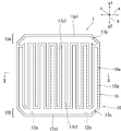
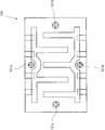
- FIG. 1 is a schematic plan view of a solar cell according to a first embodiment.
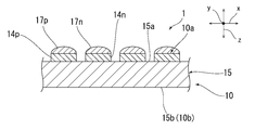
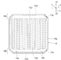
- FIG. 2 is a schematic cross-sectional view taken along line II-II in FIG. 1 is a schematic plan view of a semiconductor substrate according to a first embodiment. It is a schematic plan view of the solar cell according to the second embodiment. It is a schematic plan view of a solar cell according to a third embodiment. It is schematic-drawing sectional drawing of the solar cell which concerns on 4th Embodiment. 2 is a schematic plan view of a solar cell described in Patent Document 1.
- FIG. 1 is a schematic plan view of a solar cell according to a first embodiment.
- FIG. 2 is a schematic cross-sectional view taken along line II-II in FIG. 1 is a schematic plan view of a semiconductor substrate according to a first embodiment. It is a schematic plan view of the solar cell according to the second embodiment. It is a schematic plan view of a solar cell according to a third embodiment. It is schematic-drawing sectional drawing of the solar
- the solar cell 1 of this embodiment can also be used independently, when the solar cell 1 single-piece
- the solar cell 1 includes a solar cell substrate 10.
- the solar cell substrate 10 includes a semiconductor substrate 15, an n-type amorphous semiconductor layer 14n disposed in the first region of the back surface 15a of the semiconductor substrate 15, and a p-type amorphous semiconductor layer disposed on the second region. 14p.
- the semiconductor substrate 15 is made of single crystal silicon.
- the semiconductor substrate 15 has a rectangular shape with chamfered corners.
- the semiconductor substrate 15 includes a pair of end edge portions 15A and 15B facing in the y direction (one direction) and a pair of ends facing in the x direction (other direction) orthogonal to the y direction. And an edge.
- the semiconductor substrate 15 may have a quadrangular shape that does not have chamfered portions at corners.
- the semiconductor substrate 15 has a back surface 15a and a light receiving surface 15b.
- the semiconductor substrate 15 generates carriers by receiving light at the light receiving surface 15b.
- the carriers are holes and electrons that are generated when light is absorbed by the semiconductor substrate 15.
- the semiconductor substrate 15 is composed of a substrate made of a crystalline semiconductor having n-type or p-type conductivity.
- Specific examples of the crystalline semiconductor include crystalline silicon such as single crystal silicon and polycrystalline silicon.
- the semiconductor substrate 15 is formed of a substrate made of crystalline silicon having n-type conductivity.
- the n-type amorphous semiconductor layer 14n is formed on the first region of the back surface 15a of the semiconductor substrate 15, and the p-type amorphous semiconductor layer 14p is formed on the second region of the back surface 15a of the semiconductor substrate 15. Yes.
- each of the n-type amorphous semiconductor layer 14n and the p-type amorphous semiconductor layer 14p is formed in a comb shape.
- the back surface 10a of the solar cell substrate 10 is constituted by the surface of the n-type amorphous semiconductor layer 14n and the p-type amorphous semiconductor layer 14p and the exposed portion of the back surface 15a.
- the light receiving surface 10 b of the solar cell substrate 10 is constituted by the light receiving surface 15 b of the semiconductor substrate 15.
- the light-receiving surface 10b of the solar cell substrate 10 can also be constituted by a light-receiving surface of a passivation layer or an antireflection layer formed on substantially the entire surface of the light-receiving surface 15b of the semiconductor substrate 15.
- a semiconductor layer or a protective layer may be formed on the light receiving surface 15 b of the semiconductor substrate 15.
- a protective layer having a function as a film may be laminated in this order.
- the light receiving surface 10b of the solar cell substrate 10 is constituted by the surface of the protective layer.
- the n-type amorphous semiconductor layer 14n is formed of n-type amorphous silicon containing hydrogen.
- the p-type amorphous semiconductor layer 14p is formed of p-type amorphous silicon containing hydrogen.
- the thicknesses of the p-type and n-type amorphous semiconductor layers 14p and 14n are not particularly limited, but can be, for example, about 20 to 500 mm.
- an i-type amorphous semiconductor layer may be interposed between the semiconductor substrate 15 and the n-type amorphous semiconductor layer 14n and between the semiconductor substrate 15 and the p-type amorphous semiconductor layer 14p.
- the i-type amorphous semiconductor layer is preferably composed of an i-type amorphous silicon layer containing hydrogen.
- the thickness of the i-type amorphous silicon layer is preferably a thickness that does not substantially contribute to power generation, for example, about several to 250 inches.
- a p-side electrode 17p is provided on the p-type amorphous semiconductor layer 14p.
- an n-side electrode 17n is provided on the n-type amorphous semiconductor layer 14n.
- Each of the p-side electrode 17p and the n-side electrode 17n is arranged at a predetermined interval so as not to be electrically short-circuited.
- each of the p-side electrode 17p and the n-side electrode 17n has a comb-like shape.
- the p-side electrode 17p has a p-side bus bar portion 17p1 and a plurality of p-side finger portions 17p2.
- the p-side bus bar portion 17p1 is located at the edge portion 15A on the y1 side of the semiconductor substrate 15.
- the p-side bus bar portion 17p1 is formed in a linear shape extending along the x direction.
- the plurality of p-side finger portions 17p2 extend along the y direction from the p-side bus bar portion 17p1 toward the y2 side.
- the n-side electrode 17n has an n-side bus bar portion 17n1 and a plurality of n-side finger portions 17n2.
- the n-side bus bar portion 17n1 is located at the edge portion 15B on the y2 side of the semiconductor substrate 15.
- the n-side bus bar portion 17n1 is formed in a linear shape extending along the x direction.
- the plurality of n-side finger portions 17n2 extend along the y direction from the n-side bus bar portion 17n1 toward the y1 side.
- the plurality of n-side finger portions 17n2 and the plurality of p-side finger portions 17p2 are alternately arranged in the x direction.
- the n-side electrode 17n is an electrode that collects electrons that are majority carriers.
- the p-side electrode 17p is an electrode that collects holes that are minority carriers.
- each of the p-side electrode 17p and the n-side electrode 17n is not particularly limited.
- Each of the p-side electrode 17p and the n-side electrode 17n can be formed of, for example, a metal such as Ag, Cu, Au, Pt, Al, Sn, or Pd or an alloy containing one or more of these metals.
- the formation method of each of the p-side electrode 17p and the n-side electrode 17n is not particularly limited.
- Each of the p-side electrode 17p and the n-side electrode 17n may be formed, for example, by applying a resin-type conductive paste containing a conductive filler made of metal, an alloy, or the like, or formed by plating. May be.
- Each of the p-side electrode 17p and the n-side electrode 17n may be formed by a vapor deposition method, a sputtering method, or the like.
- a plurality of alignment marks are provided on the back surface 15 a of the semiconductor substrate 15.
- two alignment marks 12a and 12b are provided on the back surface 15a.
- the alignment marks 12a and 12b are provided on one end edge of the end edges 15A and 15B.
- the alignment marks 12a and 12b are not provided on the other edge portion.
- the alignment marks 12a and 12b are provided on the edge portion 15B where the n-side bus bar portion 17n1 of the n-side electrode 17n that collects majority carriers is disposed. More specifically, the alignment marks 12a and 12b are formed below the n-side bus bar portion 17n1 at the end edge portion 15B.
- each of the alignment marks 12a and 12b includes a recess formed on the back surface 15a of the semiconductor substrate 15 located in a portion hidden by the n-side bus bar portion 17n1.
- This recess has a depth larger than the thickness of the n-type amorphous semiconductor layer 14n. That is, the alignment marks 12a and 12b provided on the back surface 15a of the semiconductor substrate 15 are formed when the n-type and p-type amorphous semiconductor layers 14n and 14p are formed, and the n-side electrode 17n and the p-side electrode 17p are formed. In addition, it is formed to a depth that can be confirmed from the outside.
- the position of the semiconductor substrate 15 can be detected using the alignment marks 12a and 12b.
- the alignment marks 12a and 12b may be visible after the n-side electrode 17n and the p-side electrode 17p are formed, or may not be visible.
- the marks 12a and 12b are formed even after the electrodes are formed. Visible. In this case, the marks 12a and 12b can also be used as product information marks.
- the alignment mark is not limited to the one composed only of the concave portion.
- the alignment mark may include another layer formed on the back surface of the semiconductor substrate.
- the planar shape of the alignment marks 12a and 12b is not particularly limited.
- the alignment marks 12a and 12b may have a shape in which a plurality of line segments intersect such as a cross shape, for example, or may have a dot shape.
- the alignment marks 12a and 12b may have a circular shape, or may have other shapes such as a triangular shape and a rectangular shape.
- alignment marks 12 a and 12 b are formed on the back surface 15 a of the semiconductor substrate 15.
- the method for forming the alignment marks 12a and 12b is not particularly limited.
- the alignment marks 12a and 12b can be formed by removal processing by various methods such as laser irradiation, etching, or mechanical processing.
- the n-type amorphous semiconductor layer 14n is formed on the first region of the back surface 15a, and the p-type amorphous semiconductor layer 14p is formed on the second region.
- the n-type amorphous semiconductor layer 14n and the p-type amorphous semiconductor layer 14p can be formed by, for example, a CVD (Chemical Vapor Deposition) method.
- the alignment marks 12a and 12b are detected using detection means such as an imaging device, and n is determined based on the detection position.
- a type amorphous semiconductor layer 14n and a p type amorphous semiconductor layer 14p are formed. Therefore, the n-type amorphous semiconductor layer 14n and the p-type amorphous semiconductor layer 14p can be formed with high positional accuracy. Therefore, the interval between the n-type amorphous semiconductor layer 14n and the p-type amorphous semiconductor layer 14p can be reduced. Therefore, the solar cell 1 with higher photoelectric conversion efficiency can be manufactured.
- n-side electrode 17n and a p-side electrode 17p are formed.
- the n-side electrode 17n and the p-side electrode 17p can be formed by, for example, a thin film forming method such as a vacuum deposition method, a sputtering method, or a plating method, or a method using a conductive paste.
- the step of forming the n-side electrode 17n and the p-side electrode 17p as in the step of forming the n-type amorphous semiconductor layer 14n and the p-type amorphous semiconductor layer 14p, detection means such as an imaging device is used. Then, the alignment marks 12a and 12b are detected, and the n-side electrode 17n and the p-side electrode 17p are formed based on the detected positions. For this reason, the n-side electrode 17n and the p-side electrode 17p can be formed with high positional accuracy. Therefore, the solar cell 1 with higher photoelectric conversion efficiency can be manufactured.
- both the plurality of alignment marks 12a and 12b are formed on one of the edge portions 15A and 15B.
- membrane formed on alignment mark 12a, 12b is the same. For this reason, detection errors of the alignment marks 12a and 12b due to the difference in the film surface are unlikely to occur, and highly accurate position detection is possible. Therefore, the n-side electrode 17n and the p-side electrode 17p can be formed with high positional accuracy. Therefore, the photoelectric conversion efficiency of the solar cell 1 can be increased.
- both the alignment marks 12a and 12b are formed on one of the end edges 15A and 15B, so that the alignment mark of the end edge 15A and the alignment mark of the end edge 15B are different. I am letting. Specifically, the number of alignment marks is made different. And the edge part 15A and the edge part 15B can be identified by making the number of alignment marks different. For this reason, the orientation of the semiconductor substrate 15 can be easily determined. Therefore, it is possible to reduce misidentification of the orientation of the semiconductor substrate 15 in the manufacturing process of the solar cell. Such an effect can be obtained not only by the number of alignment marks but also by changing the shape, color, and the like.
- the alignment marks 12a and 12b are provided on the edge 15B where the n-side electrode 17n is provided. Since the n-side electrode 17n is an electrode that collects electrons that are majority carriers, the edge portion 15B has a small influence on the collection of minority carriers that greatly affects the photoelectric conversion characteristics. For this reason, by forming the alignment marks 12a and 12b on the electrode side that collects majority carriers, the photoelectric conversion efficiency of the solar cell 1 is unlikely to decrease even when a structural defect occurs in the edge 15B. Accordingly, it is possible to effectively suppress a decrease in photoelectric conversion efficiency due to the formation of the alignment marks 12a and 12b on the semiconductor substrate 15.
- the n-side bus bar portion 17n1 is formed on the region where the alignment marks 12a and 12b are formed. For this reason, the area
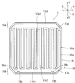
- FIG. 4 is a schematic plan view of the solar cell according to the second embodiment.
- the alignment marks 12a and 12b are provided under the n-side bus bar portion 17n1 .
- the present invention is not limited to this configuration.
- the alignment marks 12a and 12b may be formed in a region where the n-side electrode 17n and the p-side electrode 17p are not formed.
- notches 18a and 18b are formed in the n-side bus bar portion 17n1
- alignment marks 12a and 12b are formed in the notches 18a and 18b.
- the p-type amorphous semiconductor layer 14p nor the n-type amorphous semiconductor layer 14n is formed on the alignment marks 12a and 12b. For this reason, the depth of the alignment marks 12a and 12b can be made shallow. Therefore, it is possible to effectively suppress the occurrence of structural defects in the semiconductor substrate 15.
- FIG. 5 is a schematic plan view of a solar cell according to the third embodiment.
- the mark is not limited to the alignment mark.
- one product information mark 12c may be formed, or in addition to the alignment marks 12a and 12b of the first embodiment, a product information mark 12c may be formed. .
- the product information mark 12c is a mark that can identify some information about the solar cell 1 such as the date of manufacture, the production line, the lot number, the type of semiconductor substrate used, the lot number, and the like.
- the product information mark 12c may be, for example, an enumeration of numbers or a figure such as a barcode or a QR code (registered trademark).
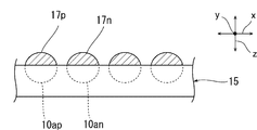
- FIG. 6 is a schematic cross-sectional view of a solar cell according to the fourth embodiment.
- the present invention is not limited to this configuration.
- a p-type dopant diffusion region 10 ap in which a p-type dopant is diffused and an n-type dopant diffusion region 10 an in which an n-type dopant is diffused are exposed on the surface.
- the n-side electrode 17n and the p-side electrode 17p may be formed immediately above the semiconductor substrate 15 using the semiconductor substrate 15 that is formed.
- the alignment marks 12a and 12b are used when forming the n-side electrode 17n and the p-side electrode 17p, and are also positioned when forming the p-type dopant diffusion region 10ap and the n-type dopant diffusion region 10an. Used as an indicator.
Landscapes
- Photovoltaic Devices (AREA)
Abstract
【課題】光電変換効率の高い太陽電池を提供する。 【解決手段】太陽電池1は、半導体基板15と、第1の電極17nと、第2の電極17pとを備えている。半導体基板15は、互いに対向している第1及び第2の端縁部15A,15Bを含む。第1の電極17nは、第1の端縁部15Bに位置している第1の部分17n1と、複数の第1の線状部17n2とを有する。第2の電極17pは、第2の端縁部15Aに位置している第2の部分17p1と、複数の第2の線状部17p2とを有する。半導体基板15は、一の主面15aにマーク12a、12bを有する。マーク12a、12bは、第1及び第2の端縁部15A,15Bの一方に形成されている。
Description
本発明は、太陽電池及びその製造方法に関する。
近年、環境に対する負荷が小さなエネルギー源として、太陽電池が大いに注目されている。このため、太陽電池に関する研究開発が活発に行われている。なかでも、太陽電池の変換効率を如何に高めるかが重要な課題となってきている。従って、向上した変換効率を有する太陽電池やその製造方法の研究開発が特に盛んに行われている。
変換効率が高い太陽電池としては、例えば下記の特許文献1などにおいて、裏面側にp型領域及びn型領域を有する所謂裏面接合型の太陽電池が提案されている。この裏面接合型の太陽電池では、キャリアを収集するための電極を受光面に設ける必要が必ずしもない。このため、裏面接合型の太陽電池では、光の受光効率を向上することができる。従って、より向上した変換効率を実現し得る。
ところで、裏面接合型太陽電池は、裏面にp型領域及びn型領域が高精細に形成される。このため裏面接合型太陽電池の製造に際しては、半導体基板の位置を正確に検出した上でp型領域、n型領域を形成する必要がある。
半導体基板の位置を検出する方向としては、例えば、半導体基板の端面の位置を検出することにより、半導体基板の位置を検出する方法や、半導体基板に形成したアライメントマークの位置を検出することにより、半導体基板の位置を検出する方法などが挙げられる。なかでも、半導体基板に形成したアライメントマークの位置を検出することにより、半導体基板の位置を検出する方法は、半導体基板の位置を高精度に検出することができる方法であるため、特に有用である。
半導体基板にアライメントマークを形成するに際しては、半導体基板のどの部位にアライメントマークを形成するかが大きな問題となる。例えば特許文献1には、図7に示すように、製造された太陽電池100の検査時に用いるアライメントマークとして、4つの端縁部のそれぞれの中央部に、アライメントマーク101a~101dを形成することが記載されている。しかしながら、4つの端縁部のそれぞれの中央部にアライメントマーク101a~101dを設けた場合、太陽電池の光電変換効率が低くなるという問題がある。
また、アライメントマーク以外のマークを半導体基板に形成する場合にも同様に、半導体基板のどの部位にマークを形成するかが問題となる。
本発明に係る太陽電池は、半導体基板と、第1の電極と、第2の電極とを備えている。半導体基板は、互いに対向している第1及び第2の端縁部を含む。第1の電極は、半導体基板の一の主面上に設けられている。第1の電極は、第1の端縁部に位置している第1の部分と、第1の部分から第2の端縁部側に向かって延びている複数の第1の線状部とを有する。第2の電極は、半導体基板の一の主面上に設けられている。第2の電極は、第2の端縁部に位置している第2の部分と、第2の部分から第1の端縁部側に向かって延びている複数の第2の線状部とを有する。半導体基板は、一の主面にマークを有する。
本発明に係る太陽電池の製造方法は、互いに対向している第1及び第2の端縁部を含み、一の主面において、第1及び第2の端縁部の一方に設けられた複数のアライメントマークを有する半導体基板と、半導体基板の一の主面上に設けられ、第1の端縁部に位置している第1の部分と、第1の部分から第2の端縁部側に向かって延びている複数の第1の線状部とを有する第1の電極と、半導体基板の一の主面上に設けられ、第2の端縁部に位置している第2の部分と、第2の部分から第1の端縁部側に向かって延びている複数の第2の線状部とを有する第2の電極とを備える太陽電池の製造方法に関する。本発明に係る太陽電池の製造方法では、複数のアライメントマークの位置を検出することにより検出した半導体基板の位置に基づいて第1及び第2の電極を形成する。
本発明によれば、改善された光電変換効率を有する太陽電池を提供することができる。
(第1の実施形態)
以下、本発明を実施した好ましい形態について、図1に示す太陽電池1を例に挙げて説明する。但し、太陽電池1は、単なる例示である。本発明に係る太陽電池及びその製造方法は、太陽電池1及びその製造方法に何ら限定されない。
以下、本発明を実施した好ましい形態について、図1に示す太陽電池1を例に挙げて説明する。但し、太陽電池1は、単なる例示である。本発明に係る太陽電池及びその製造方法は、太陽電池1及びその製造方法に何ら限定されない。
また、実施形態等において参照する各図面において、実質的に同一の機能を有する部材は同一の符号で参照することとする。また、実施形態等において参照する図面は、模式的に記載されたものである。図面に描画された物体の寸法の比率などは、現実の物体の寸法の比率などとは異なる場合がある。図面相互間においても、物体の寸法比率等が異なる場合がある。具体的な物体の寸法比率等は、以下の説明を参酌して判断されるべきである。
なお、本実施形態の太陽電池1は、単独で用いることもできるが、太陽電池1単体では、十分に大きな出力が得られない場合は、太陽電池1は、複数の太陽電池1が配線材により接続された太陽電池モジュールとして利用されることもある。
図1及び図2に示されるように、太陽電池1は、太陽電池基板10を備えている。太陽電池基板10は、半導体基板15と、半導体基板15の裏面15aの第1領域に配されたn型非晶質半導体層14nと、第2領域上に配されたp型非晶質半導体層14pとを備えている。
本実施形態では、半導体基板15は単結晶シリコンからなる。半導体基板15は、角部が面取り状である矩形状である。このため、半導体基板15は、y方向(一の方向)に対向している一対の端縁部15A,15Bと、y方向に直交するx方向(他の方向)に対向している一対の端縁部とを有している。なお、半導体基板15は、角部に面取り部を有さない四角形状の形状を有していてもよい。
半導体基板15は、裏面15aと、受光面15bとを有する。半導体基板15は、受光面15bにおいて、光を受光することによってキャリアを生成する。ここで、キャリアとは、光が半導体基板15に吸収されることにより生成される正孔及び電子のことである。半導体基板15は、n型またはp型の導電型を有する結晶性半導体からなる基板により構成されている。結晶性半導体の具体例としては、例えば、単結晶シリコン、多結晶シリコンなどの結晶シリコンが挙げられる。以下、本実施形態では、半導体基板15が、n型の導電性を有する結晶シリコンからなる基板により構成されている場合について説明する。
n型非晶質半導体層14nは、半導体基板15の裏面15aの第1領域上に形成され、p型非晶質半導体層14pは、半導体基板15の裏面15aの第2領域上に形成されている。例えば、n型非晶質半導体層14nとp型非晶質半導体層14pとのそれぞれは、くし歯状に形成されている。これらn型非晶質半導体層14n及びp型非晶質半導体層14pの表面と、裏面15aの露出部とによって、太陽電池基板10の裏面10aが構成されている。一方、太陽電池基板10の受光面10bは、半導体基板15の受光面15bによって構成されている。なお、太陽電池基板10の受光面10bは、半導体基板15の受光面15bの略全面上に形成されたパッシベーション層または反射防止層の受光面によって構成することもできる。
例えば、半導体基板15の受光面15bの上に、半導体層や保護層などが形成されていてもよい。例えば、受光面15bの上に、実質的に発電に寄与しない程度の厚みのi型非晶質半導体層と、半導体基板15と同じ導電型であるn型の非晶質半導体層と、反射抑制膜としての機能を兼ね備えた保護層とをこの順番で積層してもよい。その場合は、太陽電池基板10の受光面10bは、保護層の表面により構成されることとなる。
本実施形態において、n型非晶質半導体層14nは、水素を含むn型のアモルファスシリコンにより形成されている。一方、p型非晶質半導体層14pは、水素を含むp型のアモルファスシリコンにより形成されている。p型及びn型非晶質半導体層14p、14nのそれぞれの厚みは、特に限定されないが、例えば、20Å~500Å程度とすることができる。
なお、半導体基板15とn型非晶質半導体層14nとの間、及び半導体基板15とp型非晶質半導体層14pとの間のそれぞれに、i型非晶質半導体層を介在させてもよい。この場合、i型非晶質半導体層は、水素を含むi型のアモルファスシリコン層により構成されていることが好ましい。i型のアモルファスシリコン層の厚みは、例えば数Å~250Å程度の、発電に実質的に寄与しない程度の厚みであることが好ましい。
図2に示されるように、p型非晶質半導体層14pの上には、p側電極17pが設けられている。一方、n型非晶質半導体層14nの上には、n側電極17nが設けられている。
p側電極17p及びn側電極17nのそれぞれは、電気的に短絡しないよう互いに所定の間隔を隔てて配されている。例えば、p側電極17p及びn側電極17nのそれぞれは、くし歯状の形状にされている。p側電極17pは、p側バスバー部17p1と、複数のp側フィンガー部17p2とを有する。p側バスバー部17p1は、半導体基板15のy1側の端縁部15Aに位置している。p側バスバー部17p1は、x方向に沿って延びる線状に形成されている。複数のp側フィンガー部17p2は、p側バスバー部17p1から、y2側に向かって、y方向に沿って延びている。
n側電極17nは、n側バスバー部17n1と、複数のn側フィンガー部17n2とを有する。n側バスバー部17n1は、半導体基板15のy2側の端縁部15Bに位置している。n側バスバー部17n1は、x方向に沿って延びる線状に形成されている。複数のn側フィンガー部17n2は、n側バスバー部17n1から、y1側に向かって、y方向に沿って延びている。複数のn側フィンガー部17n2と複数のp側フィンガー部17p2とは、x方向において交互に配列されている。
上述の通り、本実施形態では、半導体基板15がn型であるため、n側電極17nが、多数キャリアである電子を収集する電極である。一方、p側電極17pが、少数キャリアである正孔を収集する電極である。
p側電極17p及びn側電極17nのそれぞれの材質は特に限定されない。p側電極17p及びn側電極17nのそれぞれは、例えば、Ag,Cu,Au,Pt,Al,Sn,Pdなどの金属やそれらの金属の一種以上を含む合金により形成することができる。p側電極17p及びn側電極17nのそれぞれの形成方法も特に限定されない。p側電極17p及びn側電極17nのそれぞれは、例えば、金属や合金などからなる導電性フィラーを含む樹脂型の導電性ペーストを塗布することにより形成されていてもよいし、めっきにより形成されていてもよい。また、p側電極17p及びn側電極17nのそれぞれは、蒸着法やスパッタ法等によって形成されていてもよい。
本実施形態において、図3に示されるように、半導体基板15の裏面15aには、複数のアライメントマークが設けられている。具体的には、裏面15aには、2つのアライメントマーク12a、12bが設けられている。アライメントマーク12a、12bは、端縁部15A及び15Bのうちの一方の端縁部に設けられている。アライメントマーク12a、12bは、他方の端縁部には設けられていない。具体的には、本実施形態では、アライメントマーク12a、12bは、多数キャリアを収集するn側電極17nのn側バスバー部17n1が配置されている端縁部15Bに設けられている。より具体的には、アライメントマーク12a、12bは、端縁部15Bにおいて、n側バスバー部17n1の下に形成されている。
本実施形態においては、アライメントマーク12a、12bのそれぞれは、n側バスバー部17n1に隠れる部分に位置する半導体基板15の裏面15aに形成された凹部を含む。この凹部は、n型非晶質半導体層14nの厚みよりも大きな深さを有する。すなわち、半導体基板15の裏面15aに設けられているアライメントマーク12a、12bは、n型及びp型非晶質半導体層14n、14pが形成され、n側電極17n及びp側電極17pを形成する際にも外部から確認可能な深さに形成されている。このため、n側電極17n及びp側電極17pの形成に際しても、アライメントマーク12a、12bを用いて半導体基板15の位置を検出することができる。なお、アライメントマーク12a、12bは、n側電極17n及びp側電極17p形成後において視認可能であってもよいし、視認不能であってもよい。マーク12a,12bに含まれる凹部の深さを、その上に積層される層全体の厚み、例えば非晶質半導体層及び電極の合計厚みより大きくすることで、電極形成後もマーク12a,12bが視認可能となる。この場合、マーク12a,12bは、製品情報マークとしても使用することができる。
本発明において、アライメントマークは、凹部のみからなるものに限定されない。例えば、アライメントマークは、半導体基板の裏面の上に形成された他の層を含んでいても良い。
アライメントマーク12a、12bの平面形状は、特に限定されない。アライメントマーク12a、12bは、例えば、十文字状等の、複数の線分が交差した形状を有していてもよいし、ドット状の形状を有していてもよい。或いは、アライメントマーク12a、12bは、円形状の形状を有していてもよいし、三角形状、矩形状等他の形状を有していてもよい。
次に、太陽電池1の製造方法の一例について説明する。
まず、半導体基板15の裏面15aにアライメントマーク12a、12bを形成する。アライメントマーク12a、12bの形成方法は、特に限定されない。アライメントマーク12a、12bは、例えば、レーザーの照射や、エッチング或いは機械的加工など種々の方法による除去加工により形成することができる。
次に、裏面15aの第1領域上にn型非晶質半導体層14nを形成し、第2領域上にp型非晶質半導体層14pを形成する。n型非晶質半導体層14n及びp型非晶質半導体層14pは、例えば、CVD(Chemical Vapor Deposition)法などにより形成することができる。
このn型非晶質半導体層14n及びp型非晶質半導体層14pを形成する工程においては、撮像装置などの検出手段を用いてアライメントマーク12a、12bを検出し、その検出位置に基づいてn型非晶質半導体層14n及びp型非晶質半導体層14pを形成する。このため、n型非晶質半導体層14n及びp型非晶質半導体層14pを高い位置精度で形成することができる。よって、n型非晶質半導体層14nとp型非晶質半導体層14pとの間の間隔を小さくすることができる。従って、光電変換効率がより高い太陽電池1の製造が可能となる。
次に、n側電極17n及びp側電極17pを形成する。n側電極17n及びp側電極17pは、例えば、真空蒸着法、スパッタリング法、めっき法などの薄膜形成方法や、導電性ペーストを用いた方法などにより形成することができる。
このn側電極17n及びp側電極17pを形成する工程においても、n型非晶質半導体層14n及びp型非晶質半導体層14pを形成する工程と同様に、撮像装置などの検出手段を用いてアライメントマーク12a、12bを検出し、その検出位置に基づいてn側電極17n及びp側電極17pを形成する。このため、n側電極17n及びp側電極17pを高い位置精度で形成することができる。従って、光電変換効率がより高い太陽電池1の製造が可能となる。
以上説明したように、本実施形態では、複数のアライメントマーク12a、12bの両方を端縁部15A,15Bのうちの一方に形成している。同じ端縁部の場合、アライメントマーク12a、12bの上に形成される膜の構成は同じである。このため、膜面の相違に起因するアライメントマーク12a、12bの検出誤差は生じにくく、高精度な位置検出が可能となる。よって、n側電極17n及びp側電極17pを高い位置精度で形成することができる。従って、太陽電池1の光電変換効率を高めることができる。
また、本実施形態は、複数のアライメントマーク12a、12bの両方を端縁部15A,15Bのうちの一方に形成することで、端縁部15Aのアライメンマークと端縁部15Bのアライメントマークを相違させている。具体的にはアライメントマークの数を相違させている。そして、アライメントマークの数を相違させることで、端縁部15Aと端縁部15Bとを識別可能としている。このため、半導体基板15の向きの判別が容易となる。従って、太陽電池の製造工程における半導体基板15の向き判別ミスを少なくすることができる。尚、このような効果は、アライメントマークの数だけでなく、形状、色等を変えることによっても得ることができる。
また、本実施形態では、n側電極17nが設けられている端縁部15Bにアライメントマーク12a、12bが設けられている。n側電極17nは、多数キャリアである電子を収集する電極であるため、端縁部15Bは、光電変換特性に大きな影響を与える少数キャリアの収集に与える影響が小さい。このため、多数キャリアを収集する電極側にアライメントマーク12a、12bを形成することによって、端縁部15Bに構造欠陥が生じた場合であっても、太陽電池1の光電変換効率が低下しにくい。従って、半導体基板15にアライメントマーク12a、12bを形成することによる光電変換効率の低下を効果的に抑制することができる。
また、本実施形態では、アライメントマーク12a、12bが形成されている領域の上に、n側バスバー部17n1が形成されている。このため、キャリアの収集可能な領域が広い。従って、より高い光電変換効率を実現することができる。
なお、さらに高い光電変換効率を得る観点からは、形成するアライメントマークの数量を1つにすることが好ましい。しかしながら、この場合は、半導体基板の位置を二次元的に確定することが困難となる。半導体基板15の位置を二次元的に正確に検出できるようにする観点からは、本実施形態のように、アライメントマークを複数設けることが好ましい。
以下、本発明を実施した好ましい形態の他の例について説明する。なお、以下の説明において、上記第1の実施形態と実質的に共通の機能を有する部材を共通の符号で参照し、説明を省略する。
(第2の実施形態)
図4は、第2の実施形態に係る太陽電池の略図的平面図である。
図4は、第2の実施形態に係る太陽電池の略図的平面図である。
上記第1の実施形態では、アライメントマーク12a、12bがn側バスバー部17n1の下に設けられている例について説明した。但し、本発明は、この構成に限定されない。例えば、図4に示されるように、アライメントマーク12a、12bは、n側電極17n及びp側電極17pが形成されていない領域に形成されていてもよい。
具体的には、本実施形態では、n側バスバー部17n1に切欠部18a、18bが形成されており、その切欠部18a、18bにアライメントマーク12a、12bが形成されている。アライメントマーク12a、12bの上には、p型非晶質半導体層14p及びn型非晶質半導体層14nも形成されていない。このため、アライメントマーク12a、12bの深さを浅くすることができる。従って、半導体基板15に構造欠陥が生じることを効果的に抑制することができる。
(第3の実施形態)
図5は、第3の実施形態に係る太陽電池の略図的平面図である。
図5は、第3の実施形態に係る太陽電池の略図的平面図である。
上記第1の実施形態では、複数のアライメントマーク12a、12bを形成する例について説明した。但し、本発明において、マークは、アライメントマークに限定されない。例えば、図5に示されるように、一つの製品情報マーク12cを形成してもよいし、上記第1の実施形態のアライメントマーク12a、12bに加えて、製品情報マーク12cを形成してもよい。
なお、製品情報マーク12cとは、製造年月日、製造ライン、ロット番号、使用した半導体基板の種類、ロット番号などの太陽電池1に関する何らかの情報が識別可能なマークである。製品情報マーク12cは、例えば、数字の羅列であってもよいし、バーコードやQRコード(登録商標)などの図形であってもよい。
(第4の実施形態)
図6は、第4の実施形態に係る太陽電池の略図的断面図である。
図6は、第4の実施形態に係る太陽電池の略図的断面図である。
上記第1の実施形態では、太陽電池基板10が、半導体基板15と、n型非晶質半導体層14nと、p型非晶質半導体層14pとにより構成されている例について説明した。但し、本発明は、この構成に限定されない。例えば、図6に示すように、p型のドーパントが拡散しているp型ドーパント拡散領域10apと、n型のドーパントが拡散しているn型ドーパント拡散領域10anとが表面に露出するように形成されている半導体基板15を用い、半導体基板15の直上にn側電極17nとp側電極17pとを形成してもよい。この場合は、アライメントマーク12a、12bは、n側電極17n及びp側電極17pの形成の際に用いられると共に、p型ドーパント拡散領域10ap及びn型ドーパント拡散領域10anの形成の際にも位置決めの指標として用いられる。
1…太陽電池
10…太陽電池基板
10an…n型ドーパント拡散領域
10ap…p型ドーパント拡散領域
12a、12b…アライメントマーク
12c…製品情報マーク
14n…n型非晶質半導体層
14p…p型非晶質半導体層
15…半導体基板
15A,15B…端縁部
15a…半導体基板の裏面
15b…半導体基板の受光面
17n…n側電極
17p…p側電極
17n1…n側バスバー部
17p1…p側バスバー部
17n2…n側フィンガー部
17p2…p側フィンガー部
10…太陽電池基板
10an…n型ドーパント拡散領域
10ap…p型ドーパント拡散領域
12a、12b…アライメントマーク
12c…製品情報マーク
14n…n型非晶質半導体層
14p…p型非晶質半導体層
15…半導体基板
15A,15B…端縁部
15a…半導体基板の裏面
15b…半導体基板の受光面
17n…n側電極
17p…p側電極
17n1…n側バスバー部
17p1…p側バスバー部
17n2…n側フィンガー部
17p2…p側フィンガー部
Claims (13)
- 互いに対向する第1の端縁部及び第2の端縁部を含む半導体基板と、
前記半導体基板の一の主面上に設けられ、前記第1の端縁部に位置している第1の部分と、前記第1の部分から前記第2の端縁部側に向かって延びている複数の第1の線状部とを有する第1の電極と、
前記半導体基板の前記一の主面上に設けられ、前記第2の端縁部に位置している第2の部分と、前記第2の部分から前記第1の端縁部側に向かって延びている複数の第2の線状部とを有する第2の電極と、
を備え、
前記半導体基板は、前記一の主面にマークを有する、
太陽電池。 - 請求項1の太陽電池であって、
前記マークは、前記半導体基板に設けられた凹部を含む。 - 請求項1または2に記載の太陽電池であって、
前記マークは、前記第1の端縁部及び第2の端縁部の一方に設けられている。 - 請求項1~3のいずれか一項に記載の太陽電池であって、
前記第1の電極は、多数キャリアを収集する電極であり、
前記第2の電極は、少数キャリアを収集する電極であり、
前記マークは、前記第1の端縁部に形成されている。 - 請求項1~4のいずれか一項に記載の太陽電池であって、
前記マークは、アライメントマークを含む。 - 請求項1~4のいずれか一項に記載の太陽電池であって、
前記マークは、製品情報マークを含む。 - 請求項1~6のいずれか一項に記載の太陽電池であって、
前記マークは、第1または第2の端縁部の、前記第1または第2の部分が設けられている部分以外の部分に形成されている。 - 請求項1~6のいずれか一項に記載の太陽電池であって、
前記マークは、前記第1または第2の部分の下に形成されている。 - 請求項1~8のいずれか一項に記載の太陽電池であって、
前記半導体基板と前記第1の電極との間に配された、第1の導電型を有する第1の半導体層と、
前記半導体基板と前記第2の電極との間に配された、第2の導電型を有する第2の半導体層と、を備える。 - 請求項9に記載の太陽電池であって、
前記マークは、前記第1及び第2の半導体層のうちの一方の半導体層の下に配されており、当該一方の半導体層の厚みよりも深い凹部を含む。 - 請求項1~8のいずれか一項に記載の太陽電池であって、
前記半導体基板は、前記一の主面に露出しているp型ドーパント拡散領域及びn型ドーパント拡散領域とを有し、
前記第1の電極が、前記p型ドーパント拡散領域及び前記n型ドーパント拡散領域のうちの一方の上に設けられ、
前記第2の電極が、前記p型ドーパント拡散領域及び前記n型ドーパント拡散領域のうちの他方の上に設けられている。 - 互いに対向する第1の端縁部及び第2の端縁部を含む半導体基板の一の主面に、アライメントマークを形成する工程と、
前記半導体基板の前記一の主面上に、前記第1の端縁部に位置している第1の部分と、前記第1の部分から前記第2の端縁部側に向かって延びている複数の第1の線状部とを有する第1の電極を形成する工程と、
前記半導体基板の前記一の主面上に、前記第2の端縁部に位置している第2の部分と、前記第2の部分から前記第1の端縁部側に向かって延びている複数の第2の線状部とを有する第2の電極を形成する工程と、を含み、
前記アライメントマークの位置を検出することにより検出した前記半導体基板の位置に基づいて、前記第1及び第2の電極を形成する、太陽電池の製造方法。 - 請求項12に記載の太陽電池の製造方法であって、
前記アライメントマークを、前記第1の端縁部及び第2の端縁部の一方の端縁部に形成する。
Applications Claiming Priority (2)
| Application Number | Priority Date | Filing Date | Title |
|---|---|---|---|
| JP2010215559A JP2012069881A (ja) | 2010-09-27 | 2010-09-27 | 太陽電池及びその製造方法 |
| JP2010-215559 | 2010-09-27 |
Publications (1)
| Publication Number | Publication Date |
|---|---|
| WO2012043508A1 true WO2012043508A1 (ja) | 2012-04-05 |
Family
ID=45892949
Family Applications (1)
| Application Number | Title | Priority Date | Filing Date |
|---|---|---|---|
| PCT/JP2011/071953 Ceased WO2012043508A1 (ja) | 2010-09-27 | 2011-09-27 | 太陽電池及びその製造方法 |
Country Status (2)
| Country | Link |
|---|---|
| JP (1) | JP2012069881A (ja) |
| WO (1) | WO2012043508A1 (ja) |
Cited By (1)
| Publication number | Priority date | Publication date | Assignee | Title |
|---|---|---|---|---|
| CN111948558A (zh) * | 2019-05-16 | 2020-11-17 | 丰田自动车株式会社 | 电池的检查方法、电池的检查装置以及电池 |
Families Citing this family (2)
| Publication number | Priority date | Publication date | Assignee | Title |
|---|---|---|---|---|
| JP7626615B2 (ja) * | 2020-12-25 | 2025-02-04 | 株式会社カネカ | 太陽電池ユニットおよび太陽電池ユニットの製造方法 |
| CN117117011A (zh) | 2023-09-19 | 2023-11-24 | 晶科能源(海宁)有限公司 | 一种电池片及光伏组件 |
Citations (5)
| Publication number | Priority date | Publication date | Assignee | Title |
|---|---|---|---|---|
| WO2006117980A1 (ja) * | 2005-04-26 | 2006-11-09 | Shin-Etsu Handotai Co., Ltd. | 太陽電池の製造方法及び太陽電池並びに半導体装置の製造方法 |
| WO2008090718A1 (ja) * | 2007-01-25 | 2008-07-31 | Sharp Kabushiki Kaisha | 太陽電池セル、太陽電池アレイおよび太陽電池モジュールならびに太陽電池アレイの製造方法 |
| WO2010068331A1 (en) * | 2008-12-10 | 2010-06-17 | Applied Materials, Inc. | Enhanced vision system for screen printing pattern alignment |
| JP2010205913A (ja) * | 2009-03-03 | 2010-09-16 | Sharp Corp | 太陽電池モジュールの製造方法、および太陽電池モジュールの製造装置 |
| WO2011090169A1 (ja) * | 2010-01-22 | 2011-07-28 | シャープ株式会社 | 裏面電極型太陽電池セル、配線シート、配線シート付き太陽電池セル、太陽電池モジュールおよび配線シート付き太陽電池セルの製造方法 |
-
2010
- 2010-09-27 JP JP2010215559A patent/JP2012069881A/ja not_active Withdrawn
-
2011
- 2011-09-27 WO PCT/JP2011/071953 patent/WO2012043508A1/ja not_active Ceased
Patent Citations (5)
| Publication number | Priority date | Publication date | Assignee | Title |
|---|---|---|---|---|
| WO2006117980A1 (ja) * | 2005-04-26 | 2006-11-09 | Shin-Etsu Handotai Co., Ltd. | 太陽電池の製造方法及び太陽電池並びに半導体装置の製造方法 |
| WO2008090718A1 (ja) * | 2007-01-25 | 2008-07-31 | Sharp Kabushiki Kaisha | 太陽電池セル、太陽電池アレイおよび太陽電池モジュールならびに太陽電池アレイの製造方法 |
| WO2010068331A1 (en) * | 2008-12-10 | 2010-06-17 | Applied Materials, Inc. | Enhanced vision system for screen printing pattern alignment |
| JP2010205913A (ja) * | 2009-03-03 | 2010-09-16 | Sharp Corp | 太陽電池モジュールの製造方法、および太陽電池モジュールの製造装置 |
| WO2011090169A1 (ja) * | 2010-01-22 | 2011-07-28 | シャープ株式会社 | 裏面電極型太陽電池セル、配線シート、配線シート付き太陽電池セル、太陽電池モジュールおよび配線シート付き太陽電池セルの製造方法 |
Cited By (2)
| Publication number | Priority date | Publication date | Assignee | Title |
|---|---|---|---|---|
| CN111948558A (zh) * | 2019-05-16 | 2020-11-17 | 丰田自动车株式会社 | 电池的检查方法、电池的检查装置以及电池 |
| CN111948558B (zh) * | 2019-05-16 | 2023-12-08 | 丰田自动车株式会社 | 电池的检查方法、电池的检查装置以及电池 |
Also Published As
| Publication number | Publication date |
|---|---|
| JP2012069881A (ja) | 2012-04-05 |
Similar Documents
| Publication | Publication Date | Title |
|---|---|---|
| JP7146805B2 (ja) | 太陽電池およびその太陽電池を備えた電子機器 | |
| CN102157612B (zh) | 太阳能电池及其制造方法 | |
| JP5820265B2 (ja) | 裏面電極型太陽電池及びその製造方法 | |
| JP2013219065A (ja) | 太陽電池及び太陽電池の製造方法 | |
| JPWO2013098955A1 (ja) | 太陽電池及びその製造方法 | |
| JP2009188355A (ja) | 太陽電池 | |
| JP6089306B2 (ja) | 太陽電池及びその製造方法 | |
| JP2012074415A (ja) | 太陽電池の製造方法 | |
| JPWO2012132835A1 (ja) | 太陽電池 | |
| JP2010283201A (ja) | 太陽電池セル、配線シート付き太陽電池セルおよび太陽電池モジュール | |
| CN120417557A (zh) | 太阳能电池和太阳能电池的制备方法 | |
| WO2012043625A1 (ja) | 太陽電池、太陽電池モジュール及び太陽電池の製造方法 | |
| JP5974300B2 (ja) | 太陽電池及びその製造方法 | |
| JP4656996B2 (ja) | 太陽電池 | |
| JP2012069881A (ja) | 太陽電池及びその製造方法 | |
| WO2013038768A1 (ja) | 太陽電池及びその製造方法 | |
| JP2015053303A (ja) | 太陽電池セル、太陽電池モジュール、および太陽電池セルの製造方法。 | |
| CN107710420B (zh) | 光电转换装置 | |
| JP2012049183A (ja) | 太陽電池及びその製造方法 | |
| TW201322467A (zh) | 太陽能電池、太陽能電池組及其製備方法 | |
| JP5172783B2 (ja) | 配線シート付き太陽電池セルおよび太陽電池モジュール | |
| JP2005260157A (ja) | 太陽電池セルおよび太陽電池モジュール | |
| WO2013027591A1 (ja) | 太陽電池及び太陽電池モジュール | |
| WO2012132595A1 (ja) | 太陽電池 | |
| JPWO2012132834A1 (ja) | 太陽電池及び太陽電池の製造方法 |
Legal Events
| Date | Code | Title | Description |
|---|---|---|---|
| 121 | Ep: the epo has been informed by wipo that ep was designated in this application |
Ref document number: 11829061 Country of ref document: EP Kind code of ref document: A1 |
|
| NENP | Non-entry into the national phase |
Ref country code: DE |
|
| 122 | Ep: pct application non-entry in european phase |
Ref document number: 11829061 Country of ref document: EP Kind code of ref document: A1 |