WO2012023243A1 - 光ピックアップ装置 - Google Patents
光ピックアップ装置 Download PDFInfo
- Publication number
- WO2012023243A1 WO2012023243A1 PCT/JP2011/004268 JP2011004268W WO2012023243A1 WO 2012023243 A1 WO2012023243 A1 WO 2012023243A1 JP 2011004268 W JP2011004268 W JP 2011004268W WO 2012023243 A1 WO2012023243 A1 WO 2012023243A1
- Authority
- WO
- WIPO (PCT)
- Prior art keywords
- housing
- cover
- optical pickup
- pickup device
- covering member
- Prior art date
- Legal status (The legal status is an assumption and is not a legal conclusion. Google has not performed a legal analysis and makes no representation as to the accuracy of the status listed.)
- Ceased
Links
Images




Classifications
-
- G—PHYSICS
- G11—INFORMATION STORAGE
- G11B—INFORMATION STORAGE BASED ON RELATIVE MOVEMENT BETWEEN RECORD CARRIER AND TRANSDUCER
- G11B7/00—Recording or reproducing by optical means, e.g. recording using a thermal beam of optical radiation by modifying optical properties or the physical structure, reproducing using an optical beam at lower power by sensing optical properties; Record carriers therefor
- G11B7/08—Disposition or mounting of heads or light sources relatively to record carriers
- G11B7/085—Disposition or mounting of heads or light sources relatively to record carriers with provision for moving the light beam into, or out of, its operative position or across tracks, otherwise than during the transducing operation, e.g. for adjustment or preliminary positioning or track change or selection
- G11B7/0857—Arrangements for mechanically moving the whole head
- G11B7/08582—Sled-type positioners
-
- G—PHYSICS
- G11—INFORMATION STORAGE
- G11B—INFORMATION STORAGE BASED ON RELATIVE MOVEMENT BETWEEN RECORD CARRIER AND TRANSDUCER
- G11B7/00—Recording or reproducing by optical means, e.g. recording using a thermal beam of optical radiation by modifying optical properties or the physical structure, reproducing using an optical beam at lower power by sensing optical properties; Record carriers therefor
- G11B7/12—Heads, e.g. forming of the optical beam spot or modulation of the optical beam
- G11B7/22—Apparatus or processes for the manufacture of optical heads, e.g. assembly
Definitions
- the present invention relates to an optical pickup device.
- the present invention relates to an optical pickup device in which a main surface of a housing is covered by a covering member.
- the optical pickup device has a function of irradiating the optical disc with laser light of a predetermined wavelength emitted from the light emitting element, and detecting the laser light reflected by the information recording layer of the optical disc with a light receiving element (Japanese Patent Application Laid-Open No. 2001-147118). As a result, the information reading operation or the writing operation is performed on the optical disc.
- a plurality of optical elements are housed in a housing.
- a flexible wiring board connected to the optical element, a control element, and the like are disposed on the top surface of the housing.
- the flexible wiring board and the control element are covered with a covering member obtained by forming a metal plate such as stainless steel into a predetermined shape.
- the covering member described above is fixed to the main surface of the housing by using an engagement means such as a screw mechanism or a hook provided at the end.
- an engagement means such as a screw mechanism or a hook provided at the end.
- the vicinity of the central part of the covering member may be deformed so as to expand outward.
- the reason for this is that the processing accuracy of the housing manufactured by injection molding a resin material or a metal material is low. Furthermore, it is one of the causes that the thermal expansion coefficients of the covering member and the housing are different.
- the outer dimensions of the optical pickup device may vary, and there may be a defect if the covering member is largely deformed.
- the optical pickup device in which the covering member bulges outward is disposed in a small space such as the inside of a notebook computer, the optical pickup device bulges outward when the optical pickup device moves under use conditions. There is also a possibility that the covering member may contact other parts.
- the present invention has been made in view of such problems, and an object of the present invention is to provide an optical pickup device in which deformation of a covering material for covering a housing is suppressed.
- An optical pickup device comprises a housing having a first main surface on which an objective lens is disposed and a second main surface facing the first main surface, an optical element housed in the housing, and the objective And a covering member for covering the first main surface of the housing in an area excluding a lens, the covering member being screwed at least in the vicinity of both ends in the longitudinal direction, and at the middle portion in the longitudinal direction It is characterized by having an engaging portion.
- the longitudinally intermediate portion of the covering member is engaged with the housing by the engaging portion. Therefore, even if the processing accuracy of the housing is not good, the outward expansion of the covering member is suppressed.
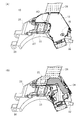
- FIG. 1 is a view showing the optical pickup device of the present invention, where (A) is a perspective view showing the optical pickup device in a state where a cover is provided, and (B) is an optical pickup device in a state where the cover is removed. It is a perspective view shown.
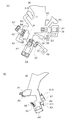
- FIG. 2A is a view showing a cover provided in the optical pickup device of the present invention
- FIG. 2B is a perspective view showing the cover in a state in which front and back are inverted.
- FIG. 3 is a view showing the optical pickup device of the present invention, and is a perspective view showing a structure in which the engaging portion of the cover engages with the projecting portion of the housing.
- FIG. 4 is a view showing the optical pickup device of the present invention, and is a perspective view showing a structure in which the engaging portion of the cover engages with the opening of the housing.
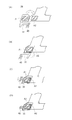
- FIG. 5 is a view showing a flexible wiring board used in the optical pickup device of the present invention, (A) is a plan view showing a state in which the flexible wiring board is developed, and (B) is a flexible state in which it is incorporated in a housing. It is a perspective view showing a wiring board.
- FIG. 6 is a cross-sectional view showing a structure in which a cover covers a portion where a package is disposed in the optical pickup device of the present invention.
- 7 is a perspective view showing a structure in which the flexible wiring board used in the optical pickup device of the present invention is bent.
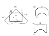
- FIG. 9 is a view showing the outer shape of the optical pickup device of the present invention.
- 10 is a view partially showing an optical disk apparatus incorporating the optical pickup device of the present invention.
- FIG. 11 is a view showing the outer shape of the optical pickup device of the present invention.
- FIG. 1A is a perspective view showing the optical pickup device of the present embodiment
- FIG. 1B is a perspective view showing the optical pickup device 10 with the cover 13 (covering member) removed.
- the main surface on which the objective lens 33 is exposed is referred to as the upper surface
- the main surface facing the upper surface is referred to as the lower surface.
- the shape of the housing 28 will be described later, it has a BOX shape, and the bottom surface has a thick bottom plate, and a side wall is provided vertically from the periphery of the bottom plate.
- the bottom plate defines the lens side as the front side and the opposite side as the back side.
- the storage side of the side wall is the inside, and the opposing surface is the outside. Furthermore, although the planar shape of the housing 28 is various, as shown in FIGS. 9 (B) and 9 (C), there is a shape in which two corners of a rectangle or a rectangle are cut if the curved portion is ignored.
- the optical pickup device 10 focuses laser light of BD (Blu-ray Disc), DVD (Digital Versatile Disc) or CD (Compact Disc) standard on the information recording layer of the optical disc (information recording medium), and this information recording is performed. It has a function of receiving the reflected light from the layer and converting it into an electrical signal.
- the optical pickup device 10 incorporates, for example, a light emitting chip for BD and a light emitting chip for DVD and CD.
- laser light emitted from the optical pickup device 10 laser light of BD standard (blue-violet wavelength band 400 nm to 420 nm), laser light of DVD standard (red wavelength band 645 nm to 675 nm) and laser light of CD standard (infrared) Wavelength band 765 nm to 805 nm).
- the optical pickup device 10 does not necessarily have to correspond to laser beams of three types of standards, and may be of a type that supports laser beams of one or two standards.
- the optical pickup device 10 covers the upper surface of a housing 28, various optical elements contained in the housing 28, a flexible wiring board 26 electrically connected to the optical element, and the housing 28 on which the objective lens 33 is disposed. And a cover 13. Incidentally, as shown in FIG. 1A, the actuator AT in which the objective lens is incorporated is exposed from the cover 13.
- the housing 28 is made of a resin material or a metal material (for example, magnesium) integrally formed by injection molding, and various optical elements are disposed on the inside and the side.
- Guide holes 30 and guide grooves 32 are provided at both end portions of the housing 28. Under use conditions, a guide shaft is inserted into the guide hole 30 and another guide shaft is engaged with the guide groove 32. Then, the optical pickup device 10 moves in the radial direction of the disc along these guide axes.
- the housing 28 has the storage space for the actuator outer shape.
- An actuator for movably holding the objective lens 33 is disposed on the top surface of the housing 28. Further, the flexible wiring board 26 is fixed to the upper surface of the housing 28 in a folded state.
- the housing 28 is provided with a laser device that emits laser light, a PDIC that receives laser light, a diffraction grating, a prism, an anamorphic lens, a mirror, and the like.
- the cover 13 is formed by bending a thin metal plate made of a metal material such as stainless steel into a predetermined shape, and covers the upper surface of the housing 28. Specifically, most of the area of the upper surface of the housing 28 is covered by the cover 13 except for the place where the actuator supporting the objective lens 33 is disposed.
- the internal space of the housing 28 in which the optical element such as a prism is incorporated is sealed by the cover 13, so that the intrusion of dust and the like from the outside into the internal space is suppressed. Furthermore, the penetration of light from the outside into the internal space of the housing 28 is also suppressed.
- the cover 13 is shaped by pressing a metal plate cut into a predetermined shape, so the dimensional accuracy is very high.
- the cover 13 is provided with a hole and an engagement portion for fixing by a screw mechanism, and the cover 13 is fixed at a predetermined position on the upper surface of the housing 28. This matter will be described later with reference to FIG. Further, an opening 15 is provided by partially opening the cover 13. The opening 15 is used to adjust the position of the built-in optical element.
- the flexible wiring board 26 connects the optical element incorporated in the optical pickup device 10 to the outside.
- the flexible wiring board 26 is fixed to the upper surface portion of the housing 28 in a state in which the flexible wiring board 26 is folded and folded a plurality of times. The specific configuration of the flexible wiring board 26 will be described later with reference to FIG.
- the flexible wiring board 34 connects the DVD, which is one of the first optical elements, and the LD for CD, and the package 22 incorporating the control element for controlling this LD, and the wiring patterns are formed on both main surfaces of the base material. Is formed.
- the wiring patterns formed on both sides of the flexible wiring substrate 34 are formed thicker than the wiring patterns formed on the flexible wiring substrate 26.
- FIG. 2A is a perspective view showing the upper surface of the cover 13
- FIG. 2B is a perspective view showing the cover 13 in a state in which the front and back are reversed.
- the cover 13 is disposed on a cover 13G for covering the upper surface of the housing, a step 13F obtained by bending the cover 13G into a step shape, a hole 13E provided at an end of the cover 13 and a peripheral portion of the cover 13G. Provided with the engaged portions 13A-13D. Furthermore, the inner end of the portion where the step portion of the cover 13 is rolled is fixed to the housing 28 or the actuator AT via an adhesive AD such as epoxy resin.
- the engaging portions 13A-13C are continuous in a state of being bent 90 degrees from the covering portion 13G, and have an L shape. These engaging portions 13A-13C engage from the outside to a portion where the side surface of the housing is partially protruded.
- the engaging portions 13A and 13B are provided near the end of the cover 13 in the longitudinal direction, and the engaging portion 13C is provided near the middle portion. Although three engaging portions 13A-13C are provided here, the number of engaging portions may be two or less, or four or more.
- the hole 13E is provided at the end of the cover 13 in order to be fixed to the upper surface of the housing by a screw mechanism.
- the holes 13E are provided only at one end, but the holes 13E may be disposed at both ends in the longitudinal direction.
- the engaging portion 13D is bent by 90 degrees continuously with the peripheral portion of the covering portion 13G, and is provided near the central portion in the longitudinal direction of the cover 13.
- the other engaging portion 13A or the like engages with the side surface of the housing, while the engaging portion 13D engages with the opening provided on the upper surface of the housing.
- the shape of the engaging portion 13D is different from that of the other engaging portions 13A and the like.
- the engaging portion 13A and the like have an L-shape that protrudes along the outer shape in order to engage with the protrusion obtained by projecting the side surface of the housing.
- the engaging portion 13D has an L shape which protrudes toward the outside of the cover 13.
- the engaging portion 13D has such a shape in order to suppress the swelling of the covering portion 13G. Further, by forming the engaging portion 13D in such a shape, the cover 13 can be easily fitted into the housing.
- a hole 13E for screwing is provided in the vicinity of one end in the longitudinal direction of the cover 13, and an engagement portion 13A is disposed in the vicinity of the other end.
- the relative position between the cover 13 and the housing is determined by screwing the hole 13E.
- the engaging portion 13A in the vicinity of the other end of the cover 13, even if the actual shape of the housing is uneven, it can be coped with by the elastic deformation of the engaging portion 13A.
- FIG. 3 a structure in which the engaging portion 13B of the cover 13 engages with the housing 28 will be described.
- the shape which the engaging part 13B engages is demonstrated, the shape which the engaging parts 13A and 13C shown to FIG. 2 (B) engage is also the same.
- the engaging portion 13B is provided by continuously bending the peripheral portion of the covering portion 13G of the cover 13 by 90 degrees.
- a projecting portion 31 is provided by partially protruding the portion corresponding to the engaging portion 13B outside the side wall of the housing 28 to the outside. Then, the cover 13 is incorporated into the housing 28 such that the inner side of the engaging portion 13B engages with the projecting portion 31 from the side and the lower side.
- the cover 13 is fixed in the thickness direction and the surface direction of the housing 28 by engaging the substantially L-shaped engaging portion 13B with the projecting portion of the housing 28.
- an opening 35 is provided by partially opening the upper center portion of the housing 28.
- the engaging portion 13D of the cover 13 is inserted into and engaged with the opening 35.
- the distal end portion 13H of the engaging portion 13D is bent outward so as to be parallel to the covering portion 13G. Therefore, when the engaging portion 13D is inserted into the opening 35, the tip end 13H of the engaging portion 13D contacts the inner wall of the housing 28 from the inside.
- the tip 13 H of the engaging portion 13 D provided near the central portion of the cover 13 is engaged with the opening 35 provided on the upper surface of the housing 28. Therefore, even if the central portion of the cover 13 tries to expand outward, the engaging portion 13D engaged with the inner wall of the opening 35 acts like a hook and the expansion thereof is prevented.
- the opening 35 is disposed near the central portion of the upper surface of the housing 28.
- engaging portion 13D is provided in the vicinity of the central portion of the cover 13, but a plurality of engaging portions 13D having similar shapes may be provided in the vicinity of the central portion of the cover 13. good.
- FIG. 5A is a plan view showing the flexible wiring board 26 in an expanded state
- FIG. 5B is a perspective view showing the flexible wiring board 26 in a state of being incorporated into the optical pickup device.
- the flexible wiring board 26 is shown with the surface on which the single layer wiring pattern is exposed as the upper surface, and in FIG. 5A and FIG. Is shown. Further, in FIG. 5A, a portion where the flexible wiring board 26 is bent is indicated by a dotted line.
- the flexible wiring board 26 is provided with a portion on which the optical elements constituting the optical pickup device 10 are mounted.
- a control element mounting unit A1 on which control elements for controlling the DVD LD and the CD LD are mounted a chip element mounting unit A2, a BD LD mounting unit A3, a PDIC mounting unit A4, an FMD mounting unit A5, A package mounting portion A6, a package mounting portion A7, a chip element mounting portion A8, a connection terminal portion A9, a connection terminal portion A10, and a chip element mounting portion A11 are provided on the flexible wiring board 26.
- Each of these parts is continuous via the wiring portion 11 of the flexible wiring board 26.
- the wiring portion 11 is formed the widest and the longest in the flexible wiring board 26.
- the one end, that is, the periphery where the chip element mounting portion A2 is provided is a rectangular area of a certain size.
- two branch wiring portions B1 and B2 are provided on the right side, and a wiring portion 11 is integrally provided on the upper side. From the left side, four branch wiring portions B3 to B6 are provided.
- Chip element mounting portions A2, A8 and A11 are provided in the wiring portions B1, B4 and B5, and chip-type resistors, capacitors or coils are mounted by solder connection.
- a package mounting portion A6 is provided in the wiring portion B7 branched from the wiring portion B5, and a volume resistance which determines the sensitivity of the FMD is disposed in the package fixed thereto.
- the wiring portion B4 includes a package mounting portion A7, in which a package incorporating a superimposed IC for placing a superimposed frequency on the current supplied to the BD LD is mounted.
- the wiring portions B1 and B3 are provided with connection terminal portions A9 and A10, in which pads made of a wiring pattern are provided, and the portions for electrically connecting with a motor or the like incorporated in the housing is there.
- the reinforcing plate 36 is made of a resin material (for example, an epoxy resin containing a fibrous filler) having a mechanical strength stronger than the base of the flexible wiring board 26. Furthermore, the reinforcing plate 36 is attached to the main surface of the base on which the wiring pattern is not provided. Here, the reinforcing plate 36 is shown by a hatched area.
- the flexible wiring board 26 By reinforcing the flexible wiring board 26 with the reinforcing plate 36, it becomes possible to stably fix the chip parts to be soldered and the like. Furthermore, since deformation and deflection of the flexible wiring board 26 are suppressed, the flexible wiring board 26 can be fixed to the housing with high accuracy.
- the flexible wiring board 26 having the above-described configuration is incorporated in the optical pickup device in a state where a plurality of bending processes are performed.
- the control element mounting portion A1 and the chip element mounting portion A2 are superimposed, and this matter will be described later with reference to FIG.
- the BD LD mounting portion A3, the chip element mounting portion A11, the chip element mounting portion A8, and the package mounting portion A7 are in a folded state, the details of which will be described later with reference to FIGS. 6 and 7.
- the FMD mounting portion A5 is bent so that the FMD faces inward
- the package mounting portion A6 beyond that is also bent so as to face inward.
- the connection terminal portion A10 is also bent so that the wiring pattern faces inward.
- the flexible wiring board 26 in a bent state is disposed on the upper surface of the housing 28 and covered with the cover 13.
- the fixing portion 38, the chip element mounting portion A2 and the control element mounting portion A1 are triple-stacked by bending the flexible wiring board 26.
- the overlapping structure will be described later with reference to FIG.
- a package 22 in which a control element for controlling the laser device is resin-sealed is mounted on the top surface of the control element mounting portion A1. And the cover 13 which covers this package 22 is made into the protrusion area 29 by providing the level
- the insertion portion 40 continuous with the fixing portion 38 of the flexible wiring board 26 and the hole 13 E of the cover 13 are fixed to the housing 28 in common using the screw 16. By this, the housing 28, the flexible wiring board 26, and the cover 13 are fixed to each other.
- a control element (LDD) for controlling the current supplied to the DVD and the CD LD is fixed in a package state.
- a chip component which is a noise countermeasure component of this LDD is fixed.
- an “L-shaped” fixing portion 38 extends roughly from the control element mounting portion A 1, and a distal end portion of the fixing portion 38 is provided with an insertion portion 40 for fixing.
- the insertion portion 40 is provided with an opening that enables screwing.
- control element mounting portion A1 is bent 180 degrees at the boundary defined between the chip element mounting portion A2 and the control element mounting portion A1 and the chip element mounting portion A2 are superimposed.
- the fixing portion 38 is bent 180 degrees at the boundary between the fixing portion 38 and the control element mounting portion A1, and the fixing portion 38 and the control element mounting portion A1 are superimposed.
- the flexible wiring board 26 is fixed to the housing by fastening means such as screws inserted into the insertion portion 40 (see FIG. 6).
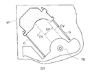
- FIG. 8 shows a part of a portable PC and a station type PC in which the optical pickup device 10 of FIG. 1 is mounted.
- the optical disc mounting table DT shown in FIG. 8 faces.
- the outside of the table DT is a BOX (MT) made of metal, and its thickness is as thin as 1 cm or less.
- a portion shown by a circle in this figure is a disk area (DA) in which the disk is arranged, and at its center is a turntable (TB) on which the disk is fixed.
- the part of the disc area (DA) is mostly made of resin, and a printed circuit board or the like is mounted on the back side.
- a cover (CV) made of metal is disposed.
- This cover (CV) is U-shaped. That is, the cover (CV) is a U-shape including the lower protrusion X, the upper protrusion Y, and the bottom Z, and an open portion (OP) in which the cover is not provided between the two protrusions. It is.
- the opening portion OP has a width that allows at least the objective lens 33 to be exposed, and is elongated in the radial direction, and the optical pickup device 10 is provided in this portion. This is an area where the optical pickup device 10 moves in the radial direction, and is open because light needs to enter and exit.
- the cover (CV) may be made of the same material as the resin cover in the disc area (DA).
- the guide shaft is inserted into the guide hole 30 and the guide groove 32, and when the optical pickup device 10 is moved, the direction of arrow B in FIG.
- the open portion of the cover (CV) has a width that allows the objective lens 33 and the holder portion of the objective lens to be exposed, and the other is covered with the cover (CV) and the resin cover of the disc area.
- a control IC 22 is disposed on the upper side of the actuator provided with the objective lens 33 with respect to the paper surface.
- the portion here is a bent portion of the flexible sheet, and at the same time an electronic component such as an IC is disposed and protrudes upward as compared with other areas.
- the portion here is the area surrounded by the dotted line in FIG. 8, which is an open portion with the cover cut away, and can be thicker than other areas. If mounting is performed in another area, the thickness of the optical pickup device 10 in the cover part is increased, so a flexible sheet or IC 22 is provided in the dotted line part, and the surface of the cover (CV) slightly bulges in the thickness direction from the middle ing.
- the thickness of the optical pick-up apparatus 10 becomes thin by that much. As a matter of course, it is a range that does not hit the optical disc. Also, as described above, it may be said that it is provided with the same degree of projection as the top of the objective lens 33.
- the flexible sheet is folded at this portion to form several layers. In addition, it is bent a lot more than other parts. Further, by bending, the pattern for disposing the IC 22 is arranged to face upward.
- the conductive pattern is thicker than the other parts by being provided with components such as a chip element, an IC, a variable resistor, and a variable capacitor. Therefore, in FIG. 1 (A), the cover 13 is formed protruding in a projecting manner.
- a flexible sheet is formed by the conductive pattern of one side one layer, it is possible to arrange a conductive pattern on the surface by folding, and prepare a multilayer sheet in which a conductive pattern is formed on both sides. There is also no.
- the planar outer shape of the optical pickup device 10 may be any shape such as a rectangle, a circle or the like.
- the planar outer shape of the optical pickup device 10 may be any shape such as a rectangle, a circle or the like.
- the angle S1 or S2 is cut to increase the moving distance of the objective lens 33 as much as possible.
- the part is curved.
- FIG. 9B is completed. This is a form in which two corners of a rectangle are cut out, and the long side L1 which is not cut off by the corners is cut by the radius of the turntable.
- the radius of the turntable may be provided on the long side L1 in a rectangular shape as shown in FIG. 9C.
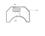
- FIG. 11 schematically shows the cover 13 of FIG.
- the objective lens 33 or the holder of the objective lens is disposed on the curved side at the center line indicated by the dotted line.
- the cover 13 is covered on the right side of the center line of the portion excluding the holder. And the upper side of the holder is raised.
- the cover 13 is capable of adjusting the position of the optical element through the hole 15, and at the same time, the flexible sheet provided on the bulging portion and the electronic parts mounted thereon have the internal components by the bulging of the cover. Protection is possible. In addition, a short circuit can be suppressed.
Landscapes
- Physics & Mathematics (AREA)
- Optics & Photonics (AREA)
- Optical Head (AREA)
Abstract
Description
13 カバー
13A 係合部
13B 係合部
13C 係合部
13D 係合部
13E 孔部
13F 段差部
15 開口部
16 ネジ
22 パッケージ
26 フレキシブル配線基板
28 ハウジング
29 突出領域
30 ガイド孔
31 突出部
32 ガイド溝
33 対物レンズ
34 フレキシブル配線基板
35 開口部
36 補強板
38 固定部
40 挿通部
B1、B2、B3、B4、B5、B6、B7 配線部
Claims (8)
- 対物レンズが配置される第1主面と前記第1主面に対向する第2主面とを備えたハウジングと、
前記ハウジングに収納される光学素子と、
前記対物レンズを除外した領域の前記ハウジングの前記第1主面を被覆する被覆部材と、を備え、
前記被覆部材は、長手方向の両端付近の少なくとも一方がネジ止めされると共に、長手方向の中間部に係合部を有することを特徴とする光ピックアップ装置。 - 前記被覆部材には、長手方向の一端付近に設けられて前記ハウジングの側面に係合する第1係合部と、長手方向の他端付近に設けられて前記ハウジングにネジ止めされる孔部と、長方向の中間部に配置されて前記ハウジングに係合する第2係合部と、が設けられることを特徴とする請求項1に記載の光ピックアップ装置。
- 前記第2係合部の先端部は、前記ハウジングの前記第1主面に設けた開口部に挿入されることを特徴とする請求項2に記載の光ピックアップ装置。
- 前記第2係合部の前記先端部は、前記ハウジングの内壁に係合ことをする請求項2または請求項3に記載の光ピックアップ装置。
- 前記ハウジングの前記第1主面には、前記光学素子と電気的に接続されるフレキシブル配線基板が配置され、
前記フレキシブル配線基板は、折り畳まれた状態で、前記被覆部材により被覆されることを特徴とする請求項1から請求項4の何れかに記載の光ピックアップ装置。 - フレキシブル配線基板に設けられた挿通部と、前記被覆部材の孔部とが、同一のネジにより前記ハウジングに固定されることを特徴とする請求項2から請求項5の何れかに記載の光ピックアップ装置。
- 前記ハウジングの前記第1主面には、前記光学素子を制御する制御素子が配置され、
前記制御素子を覆う部分の前記被覆部材には、外側に湾曲する段差加工が施されていることを特徴とする請求項1から請求項6の何れかに記載の光ピックアップ装置。 - 前記被覆部材の前記段差加工が設けられた部分の内側の端部を、接着剤を介して前記ハウジングに固定することを特徴とする請求項7に記載の光ピックアップ装置。
Priority Applications (3)
| Application Number | Priority Date | Filing Date | Title |
|---|---|---|---|
| CN201180004321.3A CN102667931B (zh) | 2010-08-18 | 2011-07-28 | 光拾取装置 |
| US13/501,412 US8819710B2 (en) | 2010-08-18 | 2011-07-28 | Optical pickup device |
| JP2012529478A JP5214063B2 (ja) | 2010-08-18 | 2011-07-28 | 光ピックアップ装置 |
Applications Claiming Priority (2)
| Application Number | Priority Date | Filing Date | Title |
|---|---|---|---|
| JP2010-182924 | 2010-08-18 | ||
| JP2010182924 | 2010-08-18 |
Publications (1)
| Publication Number | Publication Date |
|---|---|
| WO2012023243A1 true WO2012023243A1 (ja) | 2012-02-23 |
Family
ID=45604914
Family Applications (1)
| Application Number | Title | Priority Date | Filing Date |
|---|---|---|---|
| PCT/JP2011/004268 Ceased WO2012023243A1 (ja) | 2010-08-18 | 2011-07-28 | 光ピックアップ装置 |
Country Status (4)
| Country | Link |
|---|---|
| US (1) | US8819710B2 (ja) |
| JP (2) | JP5214063B2 (ja) |
| CN (1) | CN102667931B (ja) |
| WO (1) | WO2012023243A1 (ja) |
Families Citing this family (2)
| Publication number | Priority date | Publication date | Assignee | Title |
|---|---|---|---|---|
| JP5370383B2 (ja) * | 2011-01-28 | 2013-12-18 | 船井電機株式会社 | 光学素子ホルダ及びそれを備えた光ピックアップ |
| JP6634896B2 (ja) * | 2016-03-09 | 2020-01-22 | 株式会社リコー | 光照射装置、画像読取装置および画像形成装置 |
Citations (3)
| Publication number | Priority date | Publication date | Assignee | Title |
|---|---|---|---|---|
| JPH0357723U (ja) * | 1989-10-03 | 1991-06-04 | ||
| JP2006012261A (ja) * | 2004-06-24 | 2006-01-12 | Sony Corp | 光ピックアップ及びディスクドライブ装置 |
| JP2007102826A (ja) * | 2005-09-30 | 2007-04-19 | Sanyo Electric Co Ltd | 光ピックアップ装置およびその製造方法 |
Family Cites Families (4)
| Publication number | Priority date | Publication date | Assignee | Title |
|---|---|---|---|---|
| JP2611004B2 (ja) | 1989-07-27 | 1997-05-21 | 豊田合成株式会社 | 燃料注入口 |
| JPH09231597A (ja) | 1996-02-21 | 1997-09-05 | Sony Corp | 光学ピックアップ装置 |
| JP4413026B2 (ja) | 2004-01-30 | 2010-02-10 | 三洋電機株式会社 | 光ディスク装置 |
| JP2008257831A (ja) * | 2007-04-09 | 2008-10-23 | Sanyo Electric Co Ltd | 光ピックアップ装置 |
-
2011
- 2011-07-28 US US13/501,412 patent/US8819710B2/en not_active Expired - Fee Related
- 2011-07-28 WO PCT/JP2011/004268 patent/WO2012023243A1/ja not_active Ceased
- 2011-07-28 CN CN201180004321.3A patent/CN102667931B/zh not_active Expired - Fee Related
- 2011-07-28 JP JP2012529478A patent/JP5214063B2/ja not_active Expired - Fee Related
-
2012
- 2012-12-27 JP JP2012284111A patent/JP2013093095A/ja not_active Withdrawn
Patent Citations (3)
| Publication number | Priority date | Publication date | Assignee | Title |
|---|---|---|---|---|
| JPH0357723U (ja) * | 1989-10-03 | 1991-06-04 | ||
| JP2006012261A (ja) * | 2004-06-24 | 2006-01-12 | Sony Corp | 光ピックアップ及びディスクドライブ装置 |
| JP2007102826A (ja) * | 2005-09-30 | 2007-04-19 | Sanyo Electric Co Ltd | 光ピックアップ装置およびその製造方法 |
Also Published As
| Publication number | Publication date |
|---|---|
| US20120204199A1 (en) | 2012-08-09 |
| CN102667931A (zh) | 2012-09-12 |
| JP2013093095A (ja) | 2013-05-16 |
| JPWO2012023243A1 (ja) | 2013-10-28 |
| JP5214063B2 (ja) | 2013-06-19 |
| CN102667931B (zh) | 2015-05-13 |
| US8819710B2 (en) | 2014-08-26 |
Similar Documents
| Publication | Publication Date | Title |
|---|---|---|
| JP5214063B2 (ja) | 光ピックアップ装置 | |
| US6931650B2 (en) | Pickup device and disk drive | |
| CN102959629B (zh) | 光盘驱动装置及布线构造 | |
| JP2007318075A (ja) | 光学デバイス,光学デバイスの製造方法および光ピックアップ装置ならびに光ディスクドライブ装置 | |
| JP2004146441A (ja) | 半導体レーザ装置 | |
| JP5873996B2 (ja) | 光ディスク駆動装置および配線構造 | |
| US8619537B2 (en) | Optical pickup device and method of manufacturing the same | |
| CN102959630B (zh) | 光盘驱动装置 | |
| JP5338788B2 (ja) | レーザホルダ、及び、それを備えた光ピックアップ | |
| JP2012043498A (ja) | 光ピックアップ装置およびその製造方法 | |
| JP5360302B2 (ja) | 光ディスク装置 | |
| CN100461279C (zh) | 光学头及光盘驱动装置 | |
| JP2007109343A (ja) | フレキシブル・ケーブルの位置決め構造および磁気ディスク装置 | |
| JP2012027982A (ja) | 光ピックアップ装置 | |
| JP4595824B2 (ja) | 光ピックアップ装置および光ディスク装置 | |
| JP5395523B2 (ja) | 光ディスク装置 | |
| JP2012043511A (ja) | 光ピックアップ装置およびその製造方法 | |
| JP2013145613A (ja) | 光ディスク装置、および、それに用いる光ピックアップ | |
| WO2013190953A1 (ja) | 光ピックアップ装置およびそれを備えた光ディスク装置 | |
| JP2015164081A (ja) | 光ピックアップ装置 | |
| JP2015164082A (ja) | 光ピックアップ装置 | |
| JP2013145614A (ja) | 光ディスク装置、および、それに用いる光ピックアップ | |
| WO2013157333A1 (ja) | 光ピックアップ装置 | |
| JP2015164080A (ja) | 光ピックアップ装置およびそれを備えた光ディスク装置 | |
| JP2015122130A (ja) | 光ピックアップ装置 |
Legal Events
| Date | Code | Title | Description |
|---|---|---|---|
| WWE | Wipo information: entry into national phase |
Ref document number: 2012529478 Country of ref document: JP |
|
| 121 | Ep: the epo has been informed by wipo that ep was designated in this application |
Ref document number: 11817894 Country of ref document: EP Kind code of ref document: A1 |
|
| WWE | Wipo information: entry into national phase |
Ref document number: 13501412 Country of ref document: US |
|
| NENP | Non-entry into the national phase |
Ref country code: DE |
|
| 122 | Ep: pct application non-entry in european phase |
Ref document number: 11817894 Country of ref document: EP Kind code of ref document: A1 |