WO2012015046A1 - X線応力測定装置 - Google Patents
X線応力測定装置 Download PDFInfo
- Publication number
- WO2012015046A1 WO2012015046A1 PCT/JP2011/067517 JP2011067517W WO2012015046A1 WO 2012015046 A1 WO2012015046 A1 WO 2012015046A1 JP 2011067517 W JP2011067517 W JP 2011067517W WO 2012015046 A1 WO2012015046 A1 WO 2012015046A1
- Authority
- WO
- WIPO (PCT)
- Prior art keywords
- ray
- pair
- stress
- generation means
- dimensional
- Prior art date
- Legal status (The legal status is an assumption and is not a legal conclusion. Google has not performed a legal analysis and makes no representation as to the accuracy of the status listed.)
- Ceased
Links
Images






Classifications
-
- G—PHYSICS
- G01—MEASURING; TESTING
- G01N—INVESTIGATING OR ANALYSING MATERIALS BY DETERMINING THEIR CHEMICAL OR PHYSICAL PROPERTIES
- G01N23/00—Investigating or analysing materials by the use of wave or particle radiation, e.g. X-rays or neutrons, not covered by groups G01N3/00 – G01N17/00, G01N21/00 or G01N22/00
- G01N23/20—Investigating or analysing materials by the use of wave or particle radiation, e.g. X-rays or neutrons, not covered by groups G01N3/00 – G01N17/00, G01N21/00 or G01N22/00 by using diffraction of the radiation by the materials, e.g. for investigating crystal structure; by using scattering of the radiation by the materials, e.g. for investigating non-crystalline materials; by using reflection of the radiation by the materials
- G01N23/207—Diffractometry using detectors, e.g. using a probe in a central position and one or more displaceable detectors in circumferential positions
-
- G—PHYSICS
- G01—MEASURING; TESTING
- G01L—MEASURING FORCE, STRESS, TORQUE, WORK, MECHANICAL POWER, MECHANICAL EFFICIENCY, OR FLUID PRESSURE
- G01L1/00—Measuring force or stress, in general
- G01L1/25—Measuring force or stress, in general using wave or particle radiation, e.g. X-rays, microwaves, neutrons
-
- G—PHYSICS
- G01—MEASURING; TESTING
- G01L—MEASURING FORCE, STRESS, TORQUE, WORK, MECHANICAL POWER, MECHANICAL EFFICIENCY, OR FLUID PRESSURE
- G01L1/00—Measuring force or stress, in general
- G01L1/25—Measuring force or stress, in general using wave or particle radiation, e.g. X-rays, microwaves, neutrons
- G01L1/255—Measuring force or stress, in general using wave or particle radiation, e.g. X-rays, microwaves, neutrons using acoustic waves, or acoustic emission
-
- G—PHYSICS
- G01—MEASURING; TESTING
- G01N—INVESTIGATING OR ANALYSING MATERIALS BY DETERMINING THEIR CHEMICAL OR PHYSICAL PROPERTIES
- G01N23/00—Investigating or analysing materials by the use of wave or particle radiation, e.g. X-rays or neutrons, not covered by groups G01N3/00 – G01N17/00, G01N21/00 or G01N22/00
- G01N23/20—Investigating or analysing materials by the use of wave or particle radiation, e.g. X-rays or neutrons, not covered by groups G01N3/00 – G01N17/00, G01N21/00 or G01N22/00 by using diffraction of the radiation by the materials, e.g. for investigating crystal structure; by using scattering of the radiation by the materials, e.g. for investigating non-crystalline materials; by using reflection of the radiation by the materials
- G01N23/20075—Investigating or analysing materials by the use of wave or particle radiation, e.g. X-rays or neutrons, not covered by groups G01N3/00 – G01N17/00, G01N21/00 or G01N22/00 by using diffraction of the radiation by the materials, e.g. for investigating crystal structure; by using scattering of the radiation by the materials, e.g. for investigating non-crystalline materials; by using reflection of the radiation by the materials by measuring interferences of X-rays, e.g. Borrmann effect
-
- G—PHYSICS
- G01—MEASURING; TESTING
- G01B—MEASURING LENGTH, THICKNESS OR SIMILAR LINEAR DIMENSIONS; MEASURING ANGLES; MEASURING AREAS; MEASURING IRREGULARITIES OF SURFACES OR CONTOURS
- G01B15/00—Measuring arrangements characterised by the use of electromagnetic waves or particle radiation, e.g. by the use of microwaves, X-rays, gamma rays or electrons
-
- G—PHYSICS
- G01—MEASURING; TESTING
- G01L—MEASURING FORCE, STRESS, TORQUE, WORK, MECHANICAL POWER, MECHANICAL EFFICIENCY, OR FLUID PRESSURE
- G01L1/00—Measuring force or stress, in general
-
- G—PHYSICS
- G01—MEASURING; TESTING
- G01N—INVESTIGATING OR ANALYSING MATERIALS BY DETERMINING THEIR CHEMICAL OR PHYSICAL PROPERTIES
- G01N23/00—Investigating or analysing materials by the use of wave or particle radiation, e.g. X-rays or neutrons, not covered by groups G01N3/00 – G01N17/00, G01N21/00 or G01N22/00
- G01N23/20—Investigating or analysing materials by the use of wave or particle radiation, e.g. X-rays or neutrons, not covered by groups G01N3/00 – G01N17/00, G01N21/00 or G01N22/00 by using diffraction of the radiation by the materials, e.g. for investigating crystal structure; by using scattering of the radiation by the materials, e.g. for investigating non-crystalline materials; by using reflection of the radiation by the materials
Definitions
- the present invention relates to an X-ray stress measurement apparatus that measures the stress of a sample using X-rays, and in particular, can be realized as a portable apparatus because it can be configured to be relatively small and lightweight.
- the present invention relates to an X-ray stress measurement apparatus.
- an imaging plate such as a photosensitive film
- IP imaging plate
- various types of semiconductors have been used.
- X-ray detectors have been developed. For example, in Patent Document 2 below, a photon count mode (PCM) detector having a plurality of pixels, a cadmium zinc telluride (CZT) detector, an ASIC chip mounted with one or more readout circuits, and A combination of these has already been disclosed.
- PCM photon count mode
- CZT cadmium zinc telluride
- Patent Document 3 a method of monitoring a dose collected by a pixel and an X-ray detection apparatus therefor are already known in an apparatus provided with a plurality of such pixels (pixels).
- Patent Document 4 an X-ray imaging apparatus using a semiconductor X-ray array detector is already known.
- Patent Document 4 discloses a structure in which a detector is made compact and a dead space is not generated when a plurality of unit pixel detectors are arranged.
- the above-described conventional technology particularly the portable handheld X-ray diffractometer of Patent Document 1 described above, includes a plurality of semiconductors in order to detect an X-ray pattern (particularly Debye ring) diffracted by a sample. Requires a two-dimensional (area) X-ray detector or a one-dimensional (linear) detector.
- a semiconductor X-ray detector is expensive, and when combined with its related parts, it is relatively large, and is not necessarily suitable for constructing a portable handheld device. It is not configured.
- the present invention has been achieved in view of the above-described problems in the prior art, and is an X-ray stress measurement apparatus that measures the stress of a sample using X-rays, and in particular, miniaturization of the apparatus. It is an object of the present invention to provide a handheld X-ray stress measurement device that has a configuration suitable for weight reduction and is actually portable.
- an X-ray stress measuring apparatus for measuring a stress of a sample, at least at a desired angle with respect to the surface of the sample for measuring the stress.
- a pair of X-ray generation means for incident X-ray beams having an arbitrary fixed angle on the inclined plane and an incident X-ray beam from the pair of X-ray generation means
- An X-ray sensor unit for detecting a plurality of Debye rings, and a battery unit for supplying electric power to the X-ray generation unit and the semiconductor X-ray sensor unit.
- the angle formed by the mutual X-ray beams of the pair of X-ray generation means is preferably in the range of 20 degrees to 170 degrees, Furthermore, it is preferably 90 degrees.
- the X-ray sensor unit is composed of a two-dimensional X-ray detector, and further, the Debye ring detected by the two-dimensional X-ray detector causes the ring to come from any of the pair of X-ray generation means. It is preferable that a unit for determining whether the beam is caused by an X-ray beam incident on the sample is provided. Further, the two-dimensional X-ray detector is a space sandwiched between the pair of X-ray generation units. It is preferable that they are fixed at a preset position and angle with respect to the pair of X-ray generation means.
- the X-ray sensor unit is constituted by a one-dimensional X-ray detector, and the pair of X-ray generation means is further selected over time.
- the one-dimensional X-ray detector is provided in the space between the pair of X-ray generation means and the pair of X-ray generation means. It is preferably fixed at a position and angle set in advance.
- the X-ray stress measuring apparatus described above may further include a radiation shield member that houses the X-ray sensor unit together with the pair of X-ray generating means.
- a grip portion is integrally attached to the radiation shield member.
- a trigger for instructing an X-ray stress measurement operation of the X-ray stress measuring device is disposed at a position close to the gripping portion, and the battery means is disposed on the gripping portion.
- the battery means is a rechargeable battery.
- the apparatus has a configuration suitable for reducing the size and weight of the apparatus, and therefore, it is extremely excellent that it is possible to provide an actually portable handheld X-ray stress measurement apparatus. Show the effect.
- FIG. 1 shows an overall configuration of an X-ray stress measuring apparatus according to the present invention.
- reference numerals 10 and 10 ' denote an X-ray tube which is a pair of small X-ray sources provided in the apparatus, and each extends from an X-ray extraction window to form an X-ray optical path.
- Collimators 11 and 11 ′ As target material which comprises the X-ray tube 10, chromium, cobalt, iron, copper, molybdenum, or another metal material is mentioned, for example.
- slits 12 and 12 'for attaching the X-ray beam from the X-ray source to a beam having a desired diameter are attached to the tip portions of the collimators 11 and 11'.
- a filter material and a monochromator are disposed inside the collimators 11 and 11 ′, and therefore, a monochromatic X-ray beam can be obtained from the above-described X-ray source. .
- the X-ray beams (the X-ray and the X′-line, respectively) from the pair of X-ray tubes, that is, the first X-ray tube 10 and the second X-ray tube 10 ′, as is clear from the drawing,
- the X-ray beams are incident on the surface of the sample S while maintaining an arbitrary fixed angle.
- the arbitrary fixed angle formed by the pair of X-ray beams is in the range of 20 degrees to 170 degrees, and particularly preferably in the range of 70 degrees to 110 degrees.
- the light beams are incident on the surface of the sample S in directions that form an angle of 90 degrees with each other.
- the two-dimensional (area) X-ray sensor 20 includes an X-ray beam (X-ray, X ′) from the pair of X-ray tubes, that is, the first X-ray tube 10 and the second X-ray tube 10 ′.
- X-ray, X ′ X-ray beam
- the Debye rings C and C ′ diffiffraction cone
- reference numerals 13 and 13 ′ denote high voltage generators for supplying a high voltage to the first X-ray tube 10 and the second X-ray tube 10 ′, respectively. Yes. Although not shown here, each of them is composed of, for example, a large number of chip capacitors and chip diodes alternately connected on a ceramic substrate (for example, a Cockcroft-Wolton high voltage boost rectifier circuit), and the high voltage cables 14, 14 respectively. An X-ray beam is generated by supplying a high voltage to the X-ray tubes 10 and 10 'via the.
- Reference numeral 25 in the figure will be described in detail later, but a diffraction X-ray image detected by the two-dimensional (area) X-ray sensor 20, that is, part of Debye rings C and C ′.
- This is a signal processing unit for inputting an electrical signal, performing a predetermined process, and outputting the signal.
- the signal processing unit can include a CPU (Central Processing Unit), various memories, and the like.
- reference numeral 26 denotes a signal cable for transmitting an electrical signal from the X-ray sensor 20 to the signal processing unit 25.
- the components described above are covered with a resin molded product mixed with heavy metals such as tungsten (W), tantalum (Ta), and lead (Pb), for example, thereby constituting the radiation shield 100. Yes.
- a small gas pump may be disposed inside the radiation shield 100 so that the optical path of the X-ray beam (X-ray, X′-ray) can be maintained in a vacuum state. .
- a control unit 300 including a foldable display unit (for example, a liquid crystal display device) 310 is integrally attached behind the radiation shield (cover) 100 described above.
- the control unit 300 includes a control unit 320 (for example, including a CPU (Central Processing Unit) and various memories) for controlling the entire X-ray stress measurement apparatus, and although not illustrated, An input unit (various input buttons and the like) necessary for the operation is provided, and the input unit is configured.
- the display unit 310 displays the Debye ring C and C ′ (diffraction cone) images obtained by the two-dimensional (area) X-ray sensor 20 and the measurement / analysis results obtained by the signal processing unit 25. Can be displayed.
- an X-ray stress measurement operation is performed on the apparatus while the user holds the apparatus together with a power supply unit 400 for supplying necessary power to each unit of the apparatus described above.
- a trigger (switch) 450 for instructing is attached to the grip portion 460 integrally.
- symbol 410 of a figure is a storage battery (for example, rechargeable battery) which comprises the power supply part 400, and the code
- This is a power converter for inputting AC power (via adapters indicated by reference numerals 440 and 445 in the figure) through a connectable outlet 430 and converting it into DC power, and thus storing the storage battery 410.
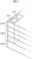
- FIG. 2 attached here shows an example of the detailed structure of the X-ray sensor unit 20 described above.
- reference numeral 210 denotes, for example, CdTe, CdZnTe, or other so-called semiconductor X-ray sensor unit, and as is apparent from the figure, it is formed in, for example, a substantially square shape of 172 ⁇ m ⁇ 172 ⁇ m. A large number (for example, 487 ⁇ 487) of pixels 211 and 211 are formed.
- an X-ray detection unit is formed at the center of each pixel, and a bias electrode for applying a negative potential is formed on one surface (upper side in the figure) of ITO (Indium Tin Oxide). )
- other transparent materials reference numeral 212 in FIG. 3
- the other surface lower surface in the figure
- Reference numeral 213) is formed.
- a reading unit 220 made of a so-called ASIC (Application Specific Integrated Circuit) having the same shape is provided on the lower surface of the semiconductor X-ray sensor unit 210 described above.
- the reading unit 220 is configured by stacking a plurality of layers (in this example, three layers), and is electrically connected between each layer by Si through vias (electrodes penetrating vertically inside the silicon semiconductor chip). By connecting them together, various circuits are three-dimensionally configured.
- a number of pads corresponding to each pixel are further provided below the readout unit 220, and further led to the wiring unit 230 including wire bonding pads.
- the number of outputs is reduced by, for example, a parallel / serial converter, a channel switch, a multiplexer, or the like provided in the interior, and via a terminal (cable) provided on the side wall. Is output.
- FIG. 3 attached includes an X-ray sensor including the above-described semiconductor X-ray sensor unit 210, the readout unit 220, the X-ray sensor 20 including the wiring unit 230, and the signal processing unit 25 described above.
- the circuit structure of the whole stress measuring device is shown. That is, reference numeral 211 in the figure indicates the bias electrode made of the above-described transparent ITO, 212 indicates the ground electrode, and 213 indicates the detection electrode.
- Reference numeral 221 in the figure denotes an amplifier for amplifying the detection signal to a desired amplitude, 222 denotes a waveform shaping circuit for shaping the waveform of the amplified signal, and 223 denotes the waveform shaping circuit.
- a comparison circuit for comparing the output of the comparison circuit with the comparison reference voltage V Ref , and 224 indicates a counting circuit for counting the output from the comparison circuit.
- the wiring unit 230 is provided with the wire bonding pad 231 described above.
- detection signals from a number of X-ray sensors (pixels) constituting the semiconductor X-ray sensor unit 210 are guided to the reading unit 220 disposed on the back surface thereof.
- the data is input to the information processing apparatus 25 including, for example, a CPU via the wiring unit 230.
- the information processing apparatus 25 executes the stress measurement / analysis process described below based on the diffraction X-ray information thus obtained, and further displays the result on the display unit (display device) 310.
- FIG. 4A shows a state in which the pair of X-ray tubes 10 and 10 ′ is viewed from the side.
- the pair of X-ray tubes 10 and 10 ′ are placed on the surface of the sample S.
- the X-ray beam and the X′-ray beam are respectively incident on the surface inclined at the angle ⁇ .
- FIG. 4B shows a state seen from the direction of arrow B in FIG.
- the angle ⁇ formed by the beam incident on the surface of the sample S from ' is set to an arbitrary fixed angle.
- the angle ⁇ formed by the pair of X-ray tube beams is fixed to one angle in the range of about 20 to 170 degrees, but may be fixed to 90 degrees, for example. When they are set to be perpendicular to each other (90 degrees), as a result, as shown in FIG. 4 (B), due to the incidence of both X-ray beams, the Debye ring C, C ′ (diffraction cone) is generated.
- the above-described two-dimensional (area) X-ray sensor 20 is disposed at a position where the pair of Debye rings C and C ′ are adjacent to or intersect each other. That is, the above-described pair of X-ray tubes (the first X-ray tube 10 and the second X-ray tube 10 ′) are arranged at a preset position and angle with respect to the semiconductor X-ray sensor unit 20.
- these are arranged symmetrically with respect to the center of the semiconductor X-ray sensor unit 20.
- Debye rings C and C ′ (diffraction cones) formed at intersecting positions can be simultaneously detected on the semiconductor X-ray sensor unit 10, and the Debye rings C and C ′ By comparing the radius or the angle of the cone ( ⁇ -2 ⁇ , ⁇ -2 ⁇ ′), it is possible to detect the presence or absence of stress in the sample S along with its direction. Alternatively, the size can be measured by comparing with the radius of the Debye ring or the cone angle ( ⁇ 2 ⁇ ) measured in advance without stress.
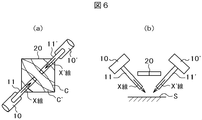
- FIGS. 5A and 5B, FIGS. 6A and 6B, and FIGS. 7A and 7B the above-described semiconductor X-ray sensor unit 20 and a pair of X-ray tubes ( Various arrangements of the first X-ray tube 10 and the second X-ray tube 10 ′) and the Debye rings C, C ′ obtained on the sensor 20 are shown. That is, FIG. 5A shows a case where a pair of X-ray tubes 10 and 10 ′ are arranged at the center on both sides of the semiconductor X-ray sensor unit 20, and X-rays and X′-rays enter the sample surface.
- FIG. 6A shows a pair of X-ray tubes 10 and 10 ′ arranged along a diagonal line of the semiconductor X-ray sensor unit 20.
- Debye rings C and C ′ are obtained along diagonal lines orthogonal to the diagonal lines, respectively.
- FIG. 7A when a pair of X-ray tubes 10 and 10 ′ are arranged along one side of the semiconductor X-ray sensor unit 20, the semiconductor X-ray sensor unit 20 is mutually connected. It can be seen that the Debye rings C and C ′ can be obtained along the diagonal line perpendicular to each other.
- the arrangement relationship between the semiconductor X-ray sensor unit 20 and the pair of X-ray tubes (the first X-ray tube 10 and the second X-ray tube 10 ′), that is, the semiconductor X-ray sensor unit 20 Since the inclination angle with respect to the X-ray and X′-ray, the distance from each pixel on the surface, etc. are already set in advance, the position of the pixel for detecting the diffracted X-ray on the semiconductor X-ray sensor unit 20 (x, According to y), the radius of the Debye rings C and C ′ or the angle of the cone ( ⁇ 2 ⁇ , ⁇ 2 ⁇ ′) can be easily specified.
- the semiconductor X-ray sensor unit 20 From the diffracted X-rays actually detected above, the radius of the Debye rings C and C ′ or the cone angles ( ⁇ 2 ⁇ , ⁇ 2 ⁇ ′) can be determined relatively easily.
- the X-ray beam detected by the pixel is one of the plurality of Debye rings C and C ′ described above. It is important to specify whether it belongs to.
- the Debye ring identification can also be executed by the information processing device 25 described above. Therefore, the Debye ring identification method when the Debye rings C and C ′ are orthogonal to each other will be described in detail below. Explained.
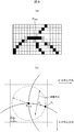
- FIG. 8A is an enlarged view showing a part of pixels formed in large numbers on the surface of the semiconductor X-ray sensor unit 20.
- the entire sensor surface is divided into a plurality of regions, and among the pixels in the region, the pixel having the strongest X-ray intensity (for example, a pixel at a point where two Debye rings C and C ′ overlap each other).
- P MAX X-ray intensity
- the next X-ray intensity for example, the maximum X
- r for example, about 20 pixels.
- a pixel (P 1 ) having an X-ray intensity that is about half of the line intensity is searched for, and a normal line direction is obtained by drawing a perpendicular to the midpoint between these two points.
- a normal line direction is obtained by drawing a perpendicular to the midpoint between these two points.
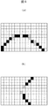
- the plurality of Debye rings detected on the surface of the semiconductor X-ray sensor unit 20 are (1) Debye ring C centered on the first X-ray tube 10 and (2) Second X-rays.
- Debye ring C ′ centered on the tube 10 ′, (3) a part resulting from both the X-ray tubes 10 and 10 ′, and (4) a part to be related to any X-ray tube are categorized. Therefore, when analyzing the Debye ring C centered on the first X-ray tube 10, as shown in the attached FIG. 9A, from a plurality of debye rings detected on the surface of the sensor unit 20, The above (2) to (4) are removed, and the above (1) Debye ring C is taken out.
- FIG. 10 in the embodiment shown in FIG. 1, in particular, as the semiconductor X-ray sensor unit, a one-dimensional linear sensor 20 ′ is used instead of the two-dimensional (area) X-ray sensor 20 described above. Some of the adopted configurations are shown. However, the other components in the figure are substantially the same as described above, and a detailed description thereof is omitted here.
- Debye rings C and C ′ (diffraction cones) formed at positions close to or intersecting each other can be detected on the semiconductor X-ray sensor unit 10, and these debye rings C and C ′. It is possible to measure the stress by measuring the radius.
- the semiconductor X-ray sensor unit by configuring the semiconductor X-ray sensor unit by adopting a one-dimensional (linear sensor) 20 ′ instead of the two-dimensional (area) X-ray sensor 20, Further downsizing and weight reduction are possible.
- the stress is measured by using the detection signal obtained from each pixel of the semiconductor X-ray sensor unit 20, the X-ray beam detected by the pixel includes the plurality of Debye rings C, It is important to specify which of C ′ belongs.
- a switch 132 is attached to the output terminal 131 of one high voltage generator 13 as shown in FIG. Then, the high voltage from one high voltage generator 13 is switched by a switch 132 attached to the output terminal 131, whereby the first X-ray tube 10 and the second X-ray tube 10 are connected via the high voltage cables 14 and 14. Sequentially supplied to the X-ray tube 10 '.
- the switching of the switch 132 is controlled, for example, in response to pressing of the trigger (switch) 450 and the control unit 320 uses the clock signal. According to this, since the first X-ray tube 10 and the second X-ray tube 10 ′ generate X-ray beams in different time zones, the one-dimensional (linear sensor) 20 ′ becomes respectively.
- a plurality of Debye rings C and C ′ can be selectively measured in a time zone. That is, even if the one-dimensional (linear sensor) 20 ′ is adopted as the semiconductor X-ray sensor unit, any one of the plurality of Debye rings C and C ′ (that is, X-rays from the first X-ray tube 10 or It is possible to reliably specify and measure whether it belongs to the X ′ line from the second X-ray tube 10 ′, and the number of high voltage generators 13 provided in the apparatus may be one. Therefore, it is particularly suitable for reducing the size and weight of the device.
- a two-dimensional (area) X-ray detector or a one-dimensional (linear) line detector that is relatively large when its related parts are combined is effectively used. This makes it possible to reduce the size and weight of the apparatus, and thus to provide an excellent effect that it is possible to provide an actually portable handheld X-ray stress measuring apparatus.
- the signal processing unit 25 for inputting a part of the Debye rings C and C ′ as an electric signal, performing a predetermined process, and outputting the electric signal is provided on the radiation shield 100.
- the present invention is not limited to this, and it may be arranged outside thereof.
- an inclination angle ⁇ with respect to the sample surface can be freely set at the distal end portion where the radiation shield 100 comes into contact with the surface of the sample S, and further, confidentiality inside the shield is ensured.
- the radiation shield 100 is further provided with an imaging means (for example, a CCD camera) for imaging the surface together with a light source that illuminates the surface of the sample.
- an imaging means for example, a CCD camera
- An image of the sample surface captured by the imaging means can be displayed on the display unit (for example, a liquid crystal display device) 310.
- the display unit for example, a liquid crystal display device
Landscapes
- Physics & Mathematics (AREA)
- Chemical & Material Sciences (AREA)
- General Physics & Mathematics (AREA)
- Health & Medical Sciences (AREA)
- Biochemistry (AREA)
- Crystallography & Structural Chemistry (AREA)
- Life Sciences & Earth Sciences (AREA)
- Analytical Chemistry (AREA)
- General Health & Medical Sciences (AREA)
- Immunology (AREA)
- Pathology (AREA)
- Toxicology (AREA)
- Acoustics & Sound (AREA)
- Analysing Materials By The Use Of Radiation (AREA)
- Measurement Of Radiation (AREA)
Abstract
Description
Claims (12)
- 試料の応力を測定するためのX線応力測定装置であって、少なくとも、
応力を測定する前記試料の表面に対して所望の角度で傾斜する平面上において、互いのX線ビームのなす角度を任意の固定角度としたX線ビームを入射する一対のX線発生手段と、
前記一対のX線発生手段からの入射X線ビームにより発生する複数のデバイリングを検出するためのX線センサ部と、そして、
前記X線発生手段及び前記半導体X線センサ部に電力を供給する電池手段とを備えているものにおいて、
前記X線センサ部は、ただ一個の二次元X線検出器又は一次元X線検出器からなり、かつ、前記少なくとも一対のX線発生手段からの入射X線ビームにより発生する複数のデバイリングが互いに隣接し、又は、交差する位置に配置されていることを特徴とするX線応力測定装置。 - 前記請求項1に記載したX線応力測定装置において、前記一対のX線発生手段の前記互いのX線ビームのなす角度は、20度~170度の範囲内であることを特徴とするX線応力測定装置。
- 前記請求項2に記載したX線応力測定装置において、前記一対のX線発生手段の前記互いのX線ビームのなす角度は、90度であることを特徴とするX線応力測定装置。
- 前記請求項1に記載したX線応力測定装置において、前記X線センサ部は二次元X線検出器により構成されると共に、更に、前記二次元X線検出器により検出されるデバイリングにより、当該リングが前記一対のX線発生手段の何れから試料に入射したX線ビームに起因するものであるかを判定する手段を備えていることを特徴とするX線応力測定装置。
- 前記請求項4に記載したX線応力測定装置において、前記二次元X線検出器は、前記一対のX線発生手段により挟まれた空間内において、当該一対のX線発生手段に対して予め設定された位置及び角度で、固定されていることを特徴とするX線応力測定装置。
- 前記請求項1に記載したX線応力測定装置において、前記X線センサ部は一次元X線検出器により構成されると共に、更に、前記一対のX線発生手段を、時間上で選択的に駆動するための手段を備えていることを特徴とするX線応力測定装置。
- 前記請求項6に記載したX線応力測定装置において、前記一次元X線検出器は、前記一対のX線発生手段との間の空間内において、当該一対のX線発生手段に対して予め設定された位置及び角度で、固定されていることを特徴とするX線応力測定装置。
- 前記請求項1に記載したX線応力測定装置において、更に、その内部に前記一対のX線発生手段と共に、前記X線センサ部を収納した放射線シールド部材を備えていることを特徴とするX線応力測定装置。
- 前記請求項8に記載したX線応力測定装置において、更に、前記放射線シールド部材には、把持部が一体的に取り付けられていることを特徴とするX線応力測定装置。
- 前記請求項9に記載したX線応力測定装置において、更に、前記把持部に近接した位置に、前記X線応力測定装置のX線応力測定動作を指示するためのトリガーが配置されていることを特徴とするX線応力測定装置。
- 前記請求項9に記載したX線応力測定装置において、更に、前記把持部には前記電池手段が内蔵されており、かつ、前記電池手段はリチャージャブルバッテリであることを特徴とするX線応力測定装置。
- 前記請求項8に記載したX線応力測定装置において、更に、前記放射線シールド部材の外部には、前記X線応力測定装置によるX線応力測定の結果を表示する表示部を備えていることを特徴とするX線応力測定装置。
Priority Applications (3)
| Application Number | Priority Date | Filing Date | Title |
|---|---|---|---|
| CA2806826A CA2806826C (en) | 2010-07-30 | 2011-07-29 | X-ray stress measuring apparatus |
| US13/812,575 US9146203B2 (en) | 2010-07-30 | 2011-07-29 | X-ray stress measuring apparatus |
| JP2012526600A JP5560338B2 (ja) | 2010-07-30 | 2011-07-29 | X線応力測定装置 |
Applications Claiming Priority (2)
| Application Number | Priority Date | Filing Date | Title |
|---|---|---|---|
| JP2010172594 | 2010-07-30 | ||
| JP2010-172594 | 2010-07-30 |
Publications (1)
| Publication Number | Publication Date |
|---|---|
| WO2012015046A1 true WO2012015046A1 (ja) | 2012-02-02 |
Family
ID=45530245
Family Applications (1)
| Application Number | Title | Priority Date | Filing Date |
|---|---|---|---|
| PCT/JP2011/067517 Ceased WO2012015046A1 (ja) | 2010-07-30 | 2011-07-29 | X線応力測定装置 |
Country Status (4)
| Country | Link |
|---|---|
| US (1) | US9146203B2 (ja) |
| JP (1) | JP5560338B2 (ja) |
| CA (1) | CA2806826C (ja) |
| WO (1) | WO2012015046A1 (ja) |
Cited By (2)
| Publication number | Priority date | Publication date | Assignee | Title |
|---|---|---|---|---|
| DE102013214397A1 (de) | 2012-07-25 | 2014-01-30 | Rigaku Corporation | Röntgenstrahl-Spannungsmessverfahren und Vorrichtung |
| JP2023538446A (ja) * | 2020-08-24 | 2023-09-07 | マルバーン パナリティカル ビー ヴィ | X線回折分析装置用x線検出器 |
Families Citing this family (5)
| Publication number | Priority date | Publication date | Assignee | Title |
|---|---|---|---|---|
| USD750783S1 (en) * | 2014-02-19 | 2016-03-01 | Rigaku Corporation | X-ray residual stress measuring instrument |
| US9870960B2 (en) | 2014-12-18 | 2018-01-16 | International Business Machines Corporation | Capacitance monitoring using X-ray diffraction |
| US9939393B2 (en) * | 2015-09-28 | 2018-04-10 | United Technologies Corporation | Detection of crystallographic properties in aerospace components |
| CN110261015A (zh) * | 2019-06-21 | 2019-09-20 | 招商局重庆交通科研设计院有限公司 | 锚索预应力自动测量系统及方法 |
| CN115598157B (zh) * | 2021-06-25 | 2025-04-11 | 中国兵器工业第五九研究所 | 一种基于阵列探测的短波长特征x射线衍射装置和方法 |
Citations (8)
| Publication number | Priority date | Publication date | Assignee | Title |
|---|---|---|---|---|
| JPS49119686A (ja) * | 1973-03-15 | 1974-11-15 | ||
| JPS5131255A (ja) * | 1974-09-10 | 1976-03-17 | Rigaku Denki Co Ltd | Atsuenhizumisokuteisochi |
| JPS63134942A (ja) * | 1986-11-27 | 1988-06-07 | Nkk Corp | メツキ鋼板の表層皮膜の機器分析法 |
| JPH02266249A (ja) * | 1989-04-06 | 1990-10-31 | Oki Electric Ind Co Ltd | 結晶面のx線回折測定方法 |
| JPH04189451A (ja) * | 1990-11-20 | 1992-07-07 | Nippon Steel Corp | シャフト付き歯車の表面加工及び評価装置 |
| JPH10185842A (ja) * | 1996-12-20 | 1998-07-14 | Toshiba Fa Syst Eng Kk | X線検査装置 |
| JP2002039970A (ja) * | 2000-07-28 | 2002-02-06 | Rigaku Corp | X線装置 |
| JP2007530979A (ja) * | 2005-03-21 | 2007-11-01 | アリベックス インコーポレイテッド | デジタルx線カメラ |
Family Cites Families (8)
| Publication number | Priority date | Publication date | Assignee | Title |
|---|---|---|---|---|
| US4489425A (en) * | 1983-01-14 | 1984-12-18 | Science Applications, Inc. | Means and method for determining residual stress on a polycrystalline sample by X-ray diffraction |
| JP3732244B2 (ja) | 1994-09-30 | 2006-01-05 | 株式会社島津製作所 | X線撮像装置 |
| JP2003066151A (ja) | 2001-08-30 | 2003-03-05 | Acrorad Co Ltd | 放射線画像検出装置 |
| US7170049B2 (en) | 2003-12-30 | 2007-01-30 | Dxray, Inc. | Pixelated cadmium zinc telluride based photon counting mode detector |
| EP1716434B1 (en) | 2004-02-11 | 2012-05-30 | Philips Intellectual Property & Standards GmbH | X-ray detector with photogates and dose control |
| US7224769B2 (en) | 2004-02-20 | 2007-05-29 | Aribex, Inc. | Digital x-ray camera |
| US7590220B1 (en) * | 2008-03-10 | 2009-09-15 | General Electric Company | X-ray inspection and detection system and method |
| US7646847B2 (en) | 2008-05-01 | 2010-01-12 | Bruker Axs Inc. | Handheld two-dimensional X-ray diffractometer |
-
2011
- 2011-07-29 CA CA2806826A patent/CA2806826C/en not_active Expired - Fee Related
- 2011-07-29 WO PCT/JP2011/067517 patent/WO2012015046A1/ja not_active Ceased
- 2011-07-29 US US13/812,575 patent/US9146203B2/en not_active Expired - Fee Related
- 2011-07-29 JP JP2012526600A patent/JP5560338B2/ja not_active Expired - Fee Related
Patent Citations (8)
| Publication number | Priority date | Publication date | Assignee | Title |
|---|---|---|---|---|
| JPS49119686A (ja) * | 1973-03-15 | 1974-11-15 | ||
| JPS5131255A (ja) * | 1974-09-10 | 1976-03-17 | Rigaku Denki Co Ltd | Atsuenhizumisokuteisochi |
| JPS63134942A (ja) * | 1986-11-27 | 1988-06-07 | Nkk Corp | メツキ鋼板の表層皮膜の機器分析法 |
| JPH02266249A (ja) * | 1989-04-06 | 1990-10-31 | Oki Electric Ind Co Ltd | 結晶面のx線回折測定方法 |
| JPH04189451A (ja) * | 1990-11-20 | 1992-07-07 | Nippon Steel Corp | シャフト付き歯車の表面加工及び評価装置 |
| JPH10185842A (ja) * | 1996-12-20 | 1998-07-14 | Toshiba Fa Syst Eng Kk | X線検査装置 |
| JP2002039970A (ja) * | 2000-07-28 | 2002-02-06 | Rigaku Corp | X線装置 |
| JP2007530979A (ja) * | 2005-03-21 | 2007-11-01 | アリベックス インコーポレイテッド | デジタルx線カメラ |
Cited By (4)
| Publication number | Priority date | Publication date | Assignee | Title |
|---|---|---|---|---|
| DE102013214397A1 (de) | 2012-07-25 | 2014-01-30 | Rigaku Corporation | Röntgenstrahl-Spannungsmessverfahren und Vorrichtung |
| US8953743B2 (en) | 2012-07-25 | 2015-02-10 | Rigaku Corporation | X-ray stress measurement method and apparatus |
| JP2023538446A (ja) * | 2020-08-24 | 2023-09-07 | マルバーン パナリティカル ビー ヴィ | X線回折分析装置用x線検出器 |
| JP7851297B2 (ja) | 2020-08-24 | 2026-04-24 | マルバーン パナリティカル ビー ヴィ | X線回折分析装置用x線検出器 |
Also Published As
| Publication number | Publication date |
|---|---|
| JPWO2012015046A1 (ja) | 2013-09-12 |
| US9146203B2 (en) | 2015-09-29 |
| CA2806826A1 (en) | 2012-02-02 |
| JP5560338B2 (ja) | 2014-07-23 |
| CA2806826C (en) | 2016-01-05 |
| US20130121470A1 (en) | 2013-05-16 |
Similar Documents
| Publication | Publication Date | Title |
|---|---|---|
| JP5560338B2 (ja) | X線応力測定装置 | |
| US7498583B2 (en) | Radiation imaging apparatus | |
| US7615757B2 (en) | Semiconductor radiological detector and semiconductor radiological imaging apparatus | |
| US9306108B2 (en) | Radiation detector | |
| CN103654814B (zh) | 放射线检测装置 | |
| CN103876766A (zh) | 利用相位步进进行差分相位对比成像的x射线拍摄系统 | |
| US20150021487A1 (en) | Two-dimensional image detecting system | |
| RU2647206C1 (ru) | Сенсорное устройство и система визуализации для обнаружения сигналов излучения | |
| CN111743556A (zh) | 放射线图像捕获装置和放射线图像捕获系统 | |
| KR20150005593A (ko) | X선 평판검출기의 제조방법 및 x선 평판검출기용 tft 어레이 기판 | |
| JP2008268038A (ja) | 半導体放射線検出器及び産業用x線ct装置 | |
| CN105051900B (zh) | 集成的二极管das探测器 | |
| JP4934826B2 (ja) | 放射線画像検出モジュールおよび放射線画像検出装置 | |
| JPWO2012015053A1 (ja) | X線回折方法及びその装置 | |
| US20050111617A1 (en) | Mammography apparatus and detecting unit | |
| CN112928108A (zh) | 用于探测器的读出芯片 | |
| JP2017518498A (ja) | モジュライメージング検出器asic | |
| JP5136736B2 (ja) | 放射線画像検出モジュールおよび放射線画像検出装置 | |
| JP2015141037A (ja) | 放射線検出器 | |
| EP4483213A1 (en) | Radiation detector and detection method | |
| JP2005121528A (ja) | 2次元イメージ素子及びそれを利用した2次元イメージ検出装置並びにx線分析装置 | |
| CN115317006A (zh) | 一种平板探测器及成像系统 | |
| JP2007155565A (ja) | 放射線画像検出モジュール | |
| JP6749723B2 (ja) | 放射線撮像装置、放射線撮像システム及び放射線撮像装置の制御方法 | |
| JP5457971B2 (ja) | 半導体x線検出器 |
Legal Events
| Date | Code | Title | Description |
|---|---|---|---|
| 121 | Ep: the epo has been informed by wipo that ep was designated in this application |
Ref document number: 11812635 Country of ref document: EP Kind code of ref document: A1 |
|
| ENP | Entry into the national phase |
Ref document number: 2806826 Country of ref document: CA |
|
| WWE | Wipo information: entry into national phase |
Ref document number: 13812575 Country of ref document: US |
|
| WWE | Wipo information: entry into national phase |
Ref document number: 2012526600 Country of ref document: JP |
|
| NENP | Non-entry into the national phase |
Ref country code: DE |
|
| 122 | Ep: pct application non-entry in european phase |
Ref document number: 11812635 Country of ref document: EP Kind code of ref document: A1 |