WO2012011585A1 - 光電変換セル及びアレイとその読み出し方法と回路 - Google Patents
光電変換セル及びアレイとその読み出し方法と回路 Download PDFInfo
- Publication number
- WO2012011585A1 WO2012011585A1 PCT/JP2011/066753 JP2011066753W WO2012011585A1 WO 2012011585 A1 WO2012011585 A1 WO 2012011585A1 JP 2011066753 W JP2011066753 W JP 2011066753W WO 2012011585 A1 WO2012011585 A1 WO 2012011585A1
- Authority
- WO
- WIPO (PCT)
- Prior art keywords
- semiconductor region
- photoelectric conversion
- potential
- cell
- output
- Prior art date
- Legal status (The legal status is an assumption and is not a legal conclusion. Google has not performed a legal analysis and makes no representation as to the accuracy of the status listed.)
- Ceased
Links
Images


Classifications
-
- H—ELECTRICITY
- H10—SEMICONDUCTOR DEVICES; ELECTRIC SOLID-STATE DEVICES NOT OTHERWISE PROVIDED FOR
- H10F—INORGANIC SEMICONDUCTOR DEVICES SENSITIVE TO INFRARED RADIATION, LIGHT, ELECTROMAGNETIC RADIATION OF SHORTER WAVELENGTH OR CORPUSCULAR RADIATION
- H10F39/00—Integrated devices, or assemblies of multiple devices, comprising at least one element covered by group H10F30/00, e.g. radiation detectors comprising photodiode arrays
- H10F39/80—Constructional details of image sensors
- H10F39/803—Pixels having integrated switching, control, storage or amplification elements
-
- H—ELECTRICITY
- H04—ELECTRIC COMMUNICATION TECHNIQUE
- H04N—PICTORIAL COMMUNICATION, e.g. TELEVISION
- H04N25/00—Circuitry of solid-state image sensors [SSIS]; Control thereof
- H04N25/60—Noise processing, e.g. detecting, correcting, reducing or removing noise
- H04N25/63—Noise processing, e.g. detecting, correcting, reducing or removing noise applied to dark current
-
- H—ELECTRICITY
- H10—SEMICONDUCTOR DEVICES; ELECTRIC SOLID-STATE DEVICES NOT OTHERWISE PROVIDED FOR
- H10F—INORGANIC SEMICONDUCTOR DEVICES SENSITIVE TO INFRARED RADIATION, LIGHT, ELECTROMAGNETIC RADIATION OF SHORTER WAVELENGTH OR CORPUSCULAR RADIATION
- H10F30/00—Individual radiation-sensitive semiconductor devices in which radiation controls the flow of current through the devices, e.g. photodetectors
- H10F30/20—Individual radiation-sensitive semiconductor devices in which radiation controls the flow of current through the devices, e.g. photodetectors the devices having potential barriers, e.g. phototransistors
- H10F30/21—Individual radiation-sensitive semiconductor devices in which radiation controls the flow of current through the devices, e.g. photodetectors the devices having potential barriers, e.g. phototransistors the devices being sensitive to infrared, visible or ultraviolet radiation
- H10F30/22—Individual radiation-sensitive semiconductor devices in which radiation controls the flow of current through the devices, e.g. photodetectors the devices having potential barriers, e.g. phototransistors the devices being sensitive to infrared, visible or ultraviolet radiation the devices having only one potential barrier, e.g. photodiodes
- H10F30/221—Individual radiation-sensitive semiconductor devices in which radiation controls the flow of current through the devices, e.g. photodetectors the devices having potential barriers, e.g. phototransistors the devices being sensitive to infrared, visible or ultraviolet radiation the devices having only one potential barrier, e.g. photodiodes the potential barrier being a PN homojunction
-
- H—ELECTRICITY
- H10—SEMICONDUCTOR DEVICES; ELECTRIC SOLID-STATE DEVICES NOT OTHERWISE PROVIDED FOR
- H10F—INORGANIC SEMICONDUCTOR DEVICES SENSITIVE TO INFRARED RADIATION, LIGHT, ELECTROMAGNETIC RADIATION OF SHORTER WAVELENGTH OR CORPUSCULAR RADIATION
- H10F39/00—Integrated devices, or assemblies of multiple devices, comprising at least one element covered by group H10F30/00, e.g. radiation detectors comprising photodiode arrays
- H10F39/10—Integrated devices
- H10F39/107—Integrated devices having multiple elements covered by H10F30/00 in a repetitive configuration, e.g. radiation detectors comprising photodiode arrays
Definitions
- the present invention relates to a photoelectric conversion cell for converting light into an electric signal and an array using the photoelectric conversion cell. Further, the present invention relates to those reading techniques.
- the dark current of the phototransistor increased equivalently due to the leakage current flowing between the collector and the isolation region and the substrate.
- the collector of the non-selected phototransistor connected to one bit line is subjected to a change in voltage when the selected phototransistor is read, and is disturbed each time another phototransistor connected to that bitline is read. It was. For this reason, there is a limit to accurate detection without information mutual interference between pixels or information detection with low illuminance.
- the thickness in the depth direction of the collector cannot be increased sufficiently, so that photoelectric conversion is performed with high sensitivity to a wavelength sensitivity close to the band gap energy of the semiconductor forming the collector. This is difficult with a semiconductor having a small light absorption coefficient in the infrared region, such as silicon.
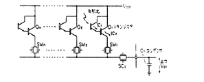
- a bipolar transistor switch for turning on / off individual collectors of the phototransistors as pixels of the phototransistor one-dimensional array 49 is connected to each collector of the one-dimensional array 48, and is common in the one-dimensional array.
- a one-dimensional linear sensor array technology for reading out photocurrent from the emitter of a connected phototransistor has been disclosed (refer to FIG. 5 of Patent Document 1. In addition, unnecessary numbers are omitted in the description).
- the collector of the phototransistor when the collector of the phototransistor is connected to the switch in the off state, the collector is in a floating potential state. When the collector of another phototransistor is connected to this, the floating potential is changed to that of the other phototransistor.
- Disturbances are generated by interacting with the accumulation state of optical information, so multiple arrays of this one-dimensional array are simply connected in two dimensions in order to create a two-dimensional array that is not in view of the two-dimensional array. It is difficult to realize a two-dimensional array with little interaction of pixel information.
- Patent Document 1 As shown in FIG. 3 (refer to FIG. 6 of Patent Document 1; numbers unnecessary for description are deleted), individual phototransistors as pixels of the phototransistor one-dimensional array 53 are shown.
- 1-dimensional linear sensor array technology for reading out photocurrent from the collectors of the phototransistors connected in common in the one-dimensional array by connecting to the individual collectors of the one-dimensional array of bipolar transistor switches for turning the emitter on / off .
- the two-dimensional array is not originally placed in the field of view, but when the emitter of the phototransistor is connected to the switch in the off state, the emitter is in a floating potential state to realize the two-dimensional array.
- an electric capacity coupled with the base of each phototransistor is provided to form a pixel, and an address is selected by a pulse applied to the base via this electric capacity and a change in the emitter potential, and a photo
- An array configuration in which the collectors of the transistors are set to a common potential has been disclosed (see FIG. 1 (a) of Non-Patent Document 2 for FIG. 4).
- this method also disturbs all non-selected pixels in which the above-mentioned capacitance is connected to one address selection line. Therefore, there is a limit to the detection of the low illuminance image signal.
- This address selection method for providing an electric capacity coupled to the base is also disclosed in FIGS. 1, 2, 3, 3, 12, 17, 20, 21, and 33 of Patent Document 2.
- FIG. 5 is a one-dimensional phototransistor array disclosed in FIG. 1 of Patent Document 3 (numbers unnecessary for explanation are deleted).
- Each of the one-dimensional phototransistors 1a, 1b, ---, and 1f The emitters are connected to the drains of the readout switches FET2a, 2b, ---, 2f and the charging switches FET3a, 3b, ---, 3f.
- the sources of the charging switch FET are collectively connected to the recharging voltage VBB .
- Lines 3 to 5 in the lower left column on page 2 of the specification indicate that the recharge switch will allow one clock time or more to elapse after reading is completed. Even with a linear sensor, two selection lines are required for each pixel. ing.
- address selection pulse noise applied to the gates of the FET 2 and FET 3 to the image signal output terminal 4 is added with the same sign as the image signal through the gate-source capacitance of the FET, and the low illumination image signal is hidden by the noise.
- FIG. 6 is a one-dimensional phototransistor array disclosed in FIG. 1 of Patent Document 4 (numbers unnecessary for the explanation are deleted), and an analog switch is used to select each pixel.
- An analog switch must apply both positive and negative transition pulses to its gate, and the pulse noise of the same sign as the readout signal must be the same as the image signal through the gate-source capacitance. In addition, the low light signal is hidden in the noise.
- the potential of the signal output line changes, it changes to the internal potential of the pixel, which not only restricts the operation of the circuit connected to the signal output line, but also causes noise in the signal output line to be read into the pixel. .
- two wires are required for each pixel, and since it is a pixel configuration that does not put the 2D array into view, it is a pixel configuration for a 2D array. Is inappropriate.
- JP 60-198959 A "Image Sensor” Japanese Unexamined Patent Publication No. 8-191143 "Photoelectric Conversion Device” Japanese Patent Laid-Open No. 2-155363 "Image Sensor” Japanese Patent Laid-Open No. 1-288181 "Semiconductor Image Sensor Device”
- the present invention is based on the above prior art.
- a photoelectric conversion cell is configured with a combination of a photoelectric conversion element and a selection element in which external noise does not easily enter, and various solutions of the above combination that are not easily affected by address selection pulse noise at the time of array reading.
- a means Means that satisfy at least one of the following 1) to 8) are provided.
- the first electric signal output unit of the photoelectric conversion element having the first electric signal output unit and the second electric signal output unit is provided in the common region.
- the photoelectric conversion cell has a configuration in which an address is selected on the second electric signal output unit side and an electric signal is extracted on the same output unit side.
- the photoelectric conversion element is a phototransistor
- a photoelectric conversion cell configuration in which an address is selected on the emitter (second electric signal output unit) side and an electric signal is extracted from the emitter side is employed.
- the collectors are phototransistors
- the collectors are formed in a common region in units of columns or rows, or an array configuration.
- the entire array portion excluding peripheral circuits can be formed in a common region or the substrate itself, and the thickness of the common region or substrate can be increased, so that detection of long wavelength light is possible. If the collectors of most photoelectric conversion elements in the array are not separated, the density of the array can be improved. Note that when the common flow region is formed by pn junction separation or dielectric separation from the substrate, blooming between pixels can be reduced.
- a photoelectric conversion element having an amplification function is used to realize F).
- a phototransistor or a photoelectric conversion element in which an amplification element such as a transistor that amplifies the electric output is combined is used.
- a cell selection element that controls the potential of the second electric signal output unit at the time of reading is connected to the second electric signal output unit of the photoelectric conversion element.
- the photoelectric conversion cell is configured. This “connection” includes a case where another element is interposed between the cell selection element and the second electric signal output portion of the photoelectric conversion element.
- the photoelectric conversion cell may be abbreviated as a cell. For example, when a bipolar transistor is used as a cell selection element, if the emitter and the photoelectric conversion element are phototransistors, the phototransistor emitter is connected. If the cell selection element is a field effect transistor, the source and the phototransistor emitter are connected. To do.
- This cell configuration reverses the sign that the cell selection pulse is superimposed on the readout electrical signal as feedthrough noise between the base / collector or gate / drain. For this reason, it becomes easy to separate the driving noise and the readout electric signal.
- a cell is constituted by a photoelectric conversion element (for example, a phototransistor) and a cell selection element.
- the cell corresponds to the pixel.
- the two-dimensional array of the present invention is formed by two-dimensionally arranging the cells of the present invention.
- the collector or drain of the selection element of each cell is connected to the electrical signal readout line of the two-dimensional array, so that the influence of the voltage change of the electrical signal readout line on the in-cell potential can be reduced.
- a photoelectric conversion element having an amplification function As one photoelectric conversion cell of the present invention, A photoelectric conversion element having an amplification function; A first transistor; It is made up of at least The photoelectric conversion element has a first electric signal output unit and a second electric signal output unit, The first transistor includes a first output unit, a second output unit, a current flowing between the first output unit and the second output unit, or a third control unit for controlling the resistance between the first output unit and the second output unit.
- the second electric signal output unit of the photoelectric conversion element has a potential difference polarity that allows an electric signal current to easily flow and a potential difference polarity that does not easily flow to the first electric signal output unit,
- the current flowing between the first output unit and the second output unit or the resistance between the first output unit and the second output unit is controlled mainly by the voltage or current between the third control unit and the second output unit,
- the second electrical signal output unit is connected to the second output unit, the first output unit is a first cell output unit, the third control unit is a first cell selection unit, By driving the first cell selection unit in the potential direction of the potential difference polarity in which the electric signal current easily flows, the electric signal of the photoelectric conversion cell is read from the first cell output unit and driven in the opposite direction to perform photoelectric conversion. Shut off the electrical signal of the cell from the first cell output, A photoelectric conversion cell A1 is provided.
- cut off the electric signal of the photoelectric conversion cell from the first cell output unit means that the electric signal of the photoelectric conversion cell is not read from the first cell output unit by setting the first transistor in a high resistance state. Means. A state in which a leak current that does not significantly affect the array operation described later flows through the first transistor is allowed.
- the first transistor serves as the cell selection element.
- the first output unit is connected to the electrical signal readout line when constituting an array.
- the photoelectric conversion element is a photoelectric conversion element capable of amplifying a photocurrent or reading a charge (accumulated charge) charged / discharged by the photocurrent as a current in order to realize high sensitivity even at low illuminance. It is called a “photoelectric conversion element having a function”. For example, a phototransistor or a bipolar transistor connected to the phototransistor and further provided with a current amplification function is used.
- a combination of a photo-resistor whose resistance changes with light irradiation and a diode or bipolar transistor, a photo field-effect transistor whose gate threshold voltage or drain-source current changes with light irradiation, or the gate potential as a reference by light irradiation A field-effect transistor that changes as viewed from the potential and a diode, if necessary, can be used.
- the potential direction of the potential difference polarity in which the electric signal current easily flows means, for example, when the photoelectric conversion element constituting the cell is a phototransistor, the second electric signal output unit is the emitter of the phototransistor.
- the potential change in the direction in which the emitter-base junction becomes the forward direction is referred to as “the potential direction of the potential difference polarity in which the electric signal current easily flows”.
- the second electrical signal output unit of the photoelectric conversion element that constitutes the cell is a diode
- the second electrical signal output unit of the photoelectric conversion element that constitutes the cell changes the potential in the direction in which the diode is in the forward direction.
- the source of a field effect transistor it means a potential change that changes in the same direction as the conductivity type of the source or channel (in the negative direction if n-type). It is not the absolute value of the potential but the direction of change.
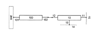
- FIG. 7 shows a schematic connection diagram of the cell A1.
- the second electric signal output unit 102 of the photoelectric conversion element 100 is connected to the second output unit 12 of the first transistor 10, and the first output unit 11 of the first transistor 10 serves as a first cell output unit.
- the third control unit 13 of the first transistor is connected to the first selection line 14 as the first cell selection unit of the cell, and the first cell output unit is configured to read the electric signal.
- the first output line 15 corresponding to the line is connected.
- the second electric signal output unit 102 of the photoelectric conversion element 100 is likely to flow a photocurrent or an amplified current (hereinafter collectively referred to as “electric signal current”) to the first electric signal output unit 101. It has a potential direction of a potential difference polarity and a potential direction of a potential difference polarity that is difficult to flow.
- the cell A1 is read by driving to the second selection potential in the potential direction of the potential difference polarity where the current easily flows, and the photoelectric conversion element 100 is connected to the first output line 15 (first output by driving to the first selection potential in the opposite direction.
- Output line 15, second output line 17, and third output line 18 are one of the above-mentioned “electrical signal readout lines”. (Including the state of leakage current that does not give)
- the first electric signal output unit 101 is connected to the first cell bias potential.
- the first electric signal output unit 101 is often provided in common with other cells.
- the second electric signal output unit potential of the photoelectric conversion element 100 is read at the second cell potential determined by the second selection potential. It is.
- the difference between the second cell potential and the second selection potential at the time of reading is the base-emitter voltage Vbe1 when the first transistor 10 is a bipolar transistor, and the first transistor 10 is a field effect transistor (FET). In some cases, it is the gate-source voltage Vgs1, and this value varies somewhat depending on the read current, but is less susceptible to changes in the potential of the first output line 15 to which the first cell output unit is connected.
- the first transistor 10 when the first transistor 10 is a field effect transistor, it is in the vicinity of the saturation region (region showing constant current output characteristics), and when the first transistor 10 is a bipolar transistor, it is active region (region showing constant current output characteristics). ) This effect is significant when operating in the vicinity.
- the cell A1 or the reading method of the configuration of the present invention can control the second cell potential, the reading accuracy is high, and the first output line 15 is not easily affected by the potential change of the first output line 15. It is difficult to receive disturbance from the first output line 15 such as noise superimposed on the first output line 15 and voltage change of a sense circuit connected to the first output line 15 at the time of reading.
- Current one of the selected pulse noises.
- a transient current caused by the pulse applied to the third control unit 13 flows from the third control unit 13 to the first output unit 15 through the parasitic capacitance existing therebetween.
- Vth1 is the gate threshold voltage of the first transistor and is negative in the case of the p channel, n Positive for channel.
- a current readout type sense amplifier is connected to the first output line 15, the sense amplifier has a signal input and a reference potential input, and the reference potential input includes the above-mentioned “(Vselect2-Vth1) on the first selection potential side. Connect the potential.
- the first transistor 10 is a field effect transistor, the operating point of the transistor moves from the saturation region to the triode region (non-saturation region). Even in such a case, the influence of the potential fluctuation on the potential change in the photoelectric conversion cell A1 is small.
- X first cell selection units of the plurality of photoelectric conversion cells A1 are connected to the first selection line 14 in the first direction, and the plurality of cells A1 are connected to the X A plurality of Y-connected first selection lines 14 are arranged in a second direction intersecting the first direction.
- the first cell output portions of the cells A1 adjacent in the second direction are connected to each other by the first output line 15 in the second direction.
- one first selection line 14 is selected from a plurality of first selection lines 14 extending in the first direction and arranged in the second direction, and a plurality of first selection lines 14 are selected.
- One first output line 15 is further selected from the first output lines 15, and an address (x, y) is specified. At this time, if one of the first selection lines 14 is selected and driven from the first selection potential to the second selection potential, electric signals are sent from all the photoelectric conversion cells A1 connected to the first selection line 14 to the photoelectric conversion cells. Read from all the first output lines 15 to which A1 is connected. In this case, a plurality of sense amplifiers are preferably connected to all the first output lines 15 (parallel reading), and their outputs are scanned. If the sense amplifier is not a current detection type but a charge or voltage detection type, the first output line 15 is sequentially connected to one or a few sense amplifiers to obtain scan output from one or a few sense amplifiers. be able to.
- a plurality of second output lines 17 are sequentially connected to the two-dimensionally arranged photoelectric conversion cell, and the two-dimensionally arranged photoelectric conversion cell B1 is read out.
- B2 the two are collectively referred to as photoelectric conversion cell B.
- a second transistor is further provided in the cell A1. That is, A photoelectric conversion element having an amplification function; A first transistor; A second transistor; It is made up of at least The photoelectric conversion element has a first electric signal output unit and a second electric signal output unit,
- the first transistor includes a first output unit, a second output unit, a current flowing between the first output unit and the second output unit, or a third control unit for controlling the resistance between the first output unit and the second output unit.
- the second transistor includes a fourth output unit, a fifth output unit, a current flowing between the fourth output unit and the fifth output unit or a resistance between the fourth output unit and the fifth output unit.
- the second electric signal output unit of the photoelectric conversion element has a potential difference polarity that allows an electric signal current to easily flow and a potential difference polarity that does not easily flow to the first electric signal output unit,
- the current flowing between the first output unit and the second output unit of the first transistor or the resistance between the first output unit and the second output unit is mainly a voltage or current between the third control unit and the second output unit.
- the second electrical signal output unit is connected to the second output unit of the first transistor;
- the fifth output of the second transistor is connected to the first output of the first transistor;
- the fourth output of the second transistor is a second cell output,
- the third control unit of the first transistor is a first cell selection unit,
- the sixth control unit of the second transistor is a second cell selection unit,
- the second cell selection unit is driven in a potential direction in which the second transistor is conductive, and the first cell selection unit is driven in a potential direction of a potential difference polarity in which the electric signal current easily flows.
- a photoelectric conversion cell B1 is provided.
- the object of the present invention is also achieved in the photoelectric conversion cell B2 in which the positions of the first transistor and the second transistor are exchanged in the photoelectric conversion cell B1. That is, A photoelectric conversion element having an amplification function; A first transistor; A second transistor; It is made up of at least The photoelectric conversion element has a first electric signal output unit and a second electric signal output unit, The first transistor includes a first output unit, a second output unit, a current flowing between the first output unit and the second output unit, or a third control unit for controlling the resistance between the first output unit and the second output unit.
- the second transistor includes a fourth output unit, a fifth output unit, a current flowing between the fourth output unit and the fifth output unit or a resistance between the fourth output unit and the fifth output unit.
- the second electric signal output unit of the photoelectric conversion element has a potential difference polarity that allows an electric signal current to easily flow and a potential difference polarity that does not easily flow to the first electric signal output unit,
- the current flowing between the first output unit and the second output unit of the first transistor or the resistance between the first output unit and the second output unit is mainly a voltage or current between the third control unit and the second output unit.
- the second electrical signal output unit is connected to the fourth output unit of the second transistor;
- the second output of the first transistor is connected to the fifth output of the second transistor;
- the first output part of the first transistor is a second cell output part,
- the third control unit of the first transistor is a first cell selection unit,
- the sixth control unit of the second transistor is a second cell selection unit,
- the second cell selection unit is driven in a potential direction in which the second transistor is conductive, and the first cell selection unit is driven in a potential direction of a potential difference polarity in which the electric signal current easily flows.
- cut off the electric signal of the photoelectric conversion cell from the second cell output unit means that the electric signal of the photoelectric conversion cell is not read from the second cell output unit with the first transistor or the second transistor in a high resistance state.
- Means state A state in which a leak current that does not greatly affect the array operation described later flows through the first and second transistors is allowed.
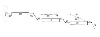
- FIG. 8 shows a schematic connection diagram of the photoelectric conversion cell B1.
- the second electric signal output unit 102 of the photoelectric conversion element 100 is connected to the second output unit 12 of the first transistor 10,
- the fifth output unit 25 of the second transistor 20 is connected to the first output unit 11 of the first transistor 10, and the fourth output unit 24 serves as the second cell output unit of the photoelectric conversion cell B1.
- the first electric signal output unit 101 of the photoelectric conversion element 100 is given a first cell bias potential 2010.
- the third control unit 13 of the first transistor 10 is connected to the first selection line 14 as the first cell selection unit of the photoelectric conversion cell B1
- the second The sixth control unit 26 of the transistor 20 is connected to the second selection line 16 of the array as the second cell selection unit of the photoelectric conversion cell B1
- the fourth cell output unit 24 is connected to the second output line 17 of the array.
- the second output line 17 can have an array configuration in which all necessary photoelectric conversion cells B1 in the array are connected by one, but the second output line 17 is provided for each photoelectric conversion cell B1 group (for example, every other column). )
- a plurality of connected cables may be provided.
- the second electric signal output unit 102 of the photoelectric conversion element 100 has a potential direction of a potential difference polarity in which an electric signal current easily flows and a potential direction of a potential difference polarity in which the electric signal current does not easily flow with respect to the first electric signal output unit 101.
- the third control unit 13 of the first transistor 10 is driven from the first selection potential to the second selection potential in the potential direction of the potential difference polarity in which the electric signal current easily flows.
- the sixth control unit 26 of the second transistor 20 is driven from the third selection potential to the fourth selection potential in the direction in which the second transistor 20 is conducted, thereby reading the photoelectric conversion cell B1.
- Driving the third control unit 13 of the first transistor 10 to the first selection potential in the reverse direction or driving the sixth control unit 26 of the second transistor 20 to the third selection potential at which the second transistor 20 is cut off To electrically cut off the photoelectric conversion element 100 from the second cell output unit.
- the first electric signal output unit 101 is often supplied with the first cell bias potential 2010.
- the third control unit 13 of the first transistor 10 is driven from the first selection potential to the second selection potential, and the second electric signal output unit potential of the photoelectric conversion element 100 Is read at the second cell potential determined by the second selection potential.
- the difference between the second cell potential and the second selection potential is the base-emitter voltage Vbe1 when the first transistor 10 is a bipolar transistor, and the gate when the first transistor 10 is a field effect transistor (FET).
- a source-to-source voltage Vgs1 varies somewhat depending on the read current, but is less susceptible to changes in the potential of the first output unit 11 of the first transistor 10. In particular, when the first transistor 10 is a field effect transistor, this effect is great when operated near the saturation region, and when the first transistor 10 is a bipolar transistor, it is operated near the active region (constant current output region).
- Vth1 is the gate threshold voltage of the first transistor 10 and is negative in the case of the p channel, Positive for n channels.
- a current readout type sense amplifier is connected to the second output line 17, the sense amplifier has a signal input and a reference potential input, and the reference potential input includes the above-mentioned “(Vselect2-Vth1) on the first selection potential side.
- the reference potential can be set. In this potential setting, when the first transistor 10 is a field effect transistor, the operating point of the transistor moves from the saturated region to the triode region (non-saturated region). The influence of the potential fluctuation on the potential change inside the photoelectric conversion cell B1 is still mitigated.
- the photoelectric conversion cell B1 or B2 can reduce the number of sense amplifiers, but requires a total of three wires, two cell selection lines and one cell output line.
- the present invention provides the following photoelectric conversion cell C1 as a novel photoelectric conversion cell capable of reducing the number of wirings. Further, since the photoelectric conversion cell C1 can set the noise accompanying the selection of the third output line 18 described below in a time series different from the signal, the influence of the noise can be almost eliminated.
- the seventh input part of the third element is connected to the first output part 11 of the first transistor 10 of the photoelectric conversion cell A1, and the eighth output part of the third element is used as the third cell output part of the photoelectric conversion cell.
- the photoelectric conversion cell C1 is configured.
- the third element is implemented by a rectifying element or a bipolar transistor, and when the third element is a rectifying element, the seventh input part is one end of the rectifying element, the eighth output part is the other end of the rectifying element, and the third element When the element is a bipolar transistor, the seventh input section is the base of the bipolar transistor, and the eighth output section is the emitter of the bipolar transistor.
- the photoelectric conversion cell is selected based on the potential of the third cell output unit and the potential of the third control unit.
- the collector (the ninth output section) is supplied with a third cell bias potential (2030 in FIG. 9) or connected to the base to perform a diode operation.
- the third cell bias potential may be shared with the first cell bias potential.
- the rectifying element can be composed of a pn junction, a hetero junction, and a Schottky junction.
- a photoelectric conversion element having an amplification function When describing the configuration of the photoelectric conversion cell C1, A photoelectric conversion element having an amplification function; A first transistor; A third element; It is made up of at least The photoelectric conversion element has a first electric signal output unit and a second electric signal output unit, The first transistor includes a first output unit, a second output unit, a current flowing between the first output unit and the second output unit, or a third control unit for controlling the resistance between the first output unit and the second output unit.
- the third element has at least a seventh input unit and an eighth output unit
- the second electric signal output unit of the photoelectric conversion element has a potential difference polarity that allows an electric signal current to easily flow and a potential difference polarity that does not easily flow to the first electric signal output unit
- the current flowing between the first output unit and the second output unit of the first transistor or the resistance between the first output unit and the second output unit is mainly a voltage or current between the third control unit and the second output unit.
- the second electrical signal output unit is connected to the second output unit of the first transistor;
- the first output of the first transistor is connected to the seventh input of the third element;
- the eighth output part of the third element is a third cell output part,
- the third control unit of the first transistor is a first cell selection unit,
- the third cell output unit is driven to a potential (sixth potential) in a direction in which the third element conducts, and the first cell selection unit is driven in a potential direction of the potential difference polarity (the second potential)
- the electrical signal of the photoelectric conversion cell is read from the third cell output unit by driving to the selection potential), and the electrical signal of the photoelectric conversion cell is driven to the third cell by driving in the opposite direction (the first selection potential).
- the potential in the direction in which the third element conducts means that when the third element is a rectifying element by changing the third cell output unit from the fifth potential to the sixth potential, the junction is in order.
- the third element is a transistor biased in the direction, it is a potential in the direction in which the emitter junction is forward-biased (sixth potential).
- the potential in the direction in which the third element is cut off is
- the third element is a rectifying element by changing the third cell output unit from the sixth potential to the fifth potential
- the junction is reverse-biased, and when the third element is a transistor of the third element
- the emitter junction has a potential (fifth potential) in the direction in which it is reverse-biased.
- the change in potential is important.
- shut off the electrical output of the photoelectric conversion cell from the third cell output unit means that the electrical signal of the photoelectric conversion cell is read from the third cell output unit with the first transistor or the third element in a high resistance state. It means that there is no state. A state in which a leak current that does not greatly affect the array operation described later flows through the first transistor and the third element is allowed.
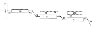
- FIG. 9 is a schematic connection diagram of the photoelectric conversion cell C1.
- the second electric signal output unit 102 of the photoelectric conversion element 100 is connected to the second output unit 12 of the first transistor 10,
- the seventh input part 37 of the third element 30 is connected to the first output part 11 of the first transistor 10, and the eighth output part 38 becomes the third cell output part of the photoelectric conversion cell C1.
- the first cell bias potential 2010 is applied to the first electric signal output unit 101 of the photoelectric conversion element 100.
- the third element 30 is a bipolar transistor
- a third cell bias 2030 is applied to the ninth output section 39 (collector).
- the third cell bias can be common to the first cell bias 2010.
- the third control unit 13 of the first transistor 10 is connected to the first selection line 14 as the first cell selection unit of the photoelectric conversion cell C1
- the third The eighth output section 38 of the element 30 is a third cell output section and is connected to the third output line 18 of the array.
- the third output lines 18 of the array are arranged in parallel in a number close to the number of photoelectric conversion cells provided in the first direction of the array.
- the dummy photoelectric conversion cell provided as a countermeasure for the peripheral pattern effect of lithography does not necessarily need to be connected to the third output line 18. The same applies to other arrays.
- the second electric signal output unit 102 of the photoelectric conversion element 100 has a potential difference polarity in which the electric signal current (photocurrent or current obtained by amplifying it) of the photoelectric conversion element 100 easily flows to the first electric signal output unit 101.
- the third cell output unit of the photoelectric conversion cell C1 is driven from the fifth output potential to the sixth output potential through the third output line 18 to which the photoelectric conversion cell C1 is connected.
- the change from the fifth output potential to the sixth output potential is a change in the direction in which the seventh input unit 37 and the eighth output unit 38 of the third element 30 are electrically connected.
- the third output line 18 is put in a floating state,
- the first cell selection unit of the photoelectric conversion cell C1 that is the third control unit 13 of the first transistor 10 through the first selection line 14 is connected to the electric signal current (photocurrent or photoelectric current) of the photoelectric conversion element 100 from the first selection potential.
- the photoelectric conversion cell C1 is read by driving to the second selection potential in the potential direction of the potential difference polarity in which the amplified current) easily flows.
- the third control unit 13 of the first transistor 10 is driven from the first selection potential to the second selection potential, and the second electric signal output unit potential of the photoelectric conversion element 100 Is read at the second cell potential determined by the second selection potential.
- the difference between the second cell potential and the second selection potential is the base-emitter voltage Vbe1 when the first transistor 10 is a bipolar transistor, and the gate when the first transistor 10 is a field effect transistor (FET).
- a source-to-source voltage Vgs1 varies somewhat depending on the read current, but is less susceptible to changes in the potential of the first output unit 11 of the first transistor 10. In particular, when the first transistor 10 is a field effect transistor, this effect is great when operated near the saturation region, and when the first transistor 10 is a bipolar transistor, it is operated near the active region (constant current output region).
- the resistance of the first transistor 10 viewed from the second electric signal output terminal 102 of the photoelectric conversion element 100 increases as the read current of the electric signal decreases, and the read time decreases.
- Vth1 is the gate threshold voltage of the first transistor 10 and is negative in the case of the p channel
- Vbe3 is a base-emitter voltage when the third element 30 is a bipolar transistor
- Vd is a forward voltage when the third element 30 is a rectifying element.
- a current readout type sense amplifier is connected to the third output line 18, and the sense amplifier has a signal input and a reference potential input, and the reference potential input includes “(Vselect2-Vth1-Vbe (or Vd))”. It is possible to connect the “potential on the first selection side”.
- the first transistor 10 is a field effect transistor, the operating point of the transistor moves from the saturated region to the triode region (non-saturated region). The influence of the potential fluctuation on the potential change inside the photoelectric conversion cell C1 is still small.
- the photoelectric conversion cell A1 constitutes the following array. That is, A plurality of first selection lines extending in a first direction; A plurality of first output lines extending in a second direction intersecting the first direction; It is composed of at least a plurality of photoelectric conversion cells A1,
- the photoelectric conversion cell A1 has a first cell selection unit and a first cell output unit, The plurality of photoelectric conversion cells A1 are arranged in the first direction and the second direction, The first cell selection units of the plurality of photoelectric conversion cells A1 arranged in the first direction and forming one row are respectively connected to one of the plurality of first selection lines,
- the photoelectric conversion array R1A wherein first cell output portions of the plurality of photoelectric conversion cells arranged in the second direction and forming one column are respectively connected to one of the plurality of first output lines.
- the photoelectric conversion cell B1 or B2 constitutes the following array. That is, A plurality of first selection lines extending in a first direction; A plurality of second selection lines extending in a second direction intersecting the first direction; At least one second output line and a plurality of photoelectric conversion cells B1 or a plurality of photoelectric conversion cells B2 are configured at least,
- the photoelectric conversion cell B1 or B2 has a first cell selection unit, a second cell selection unit, and a second cell output unit,
- the plurality of photoelectric conversion cells B1 or B2 are arranged in the first direction and the second direction,
- the first cell selectors of the plurality of photoelectric conversion cells B1 or B2 arranged in the first direction and forming one row are respectively connected to one of the plurality of first selection lines
- the second cell selectors of the plurality of photoelectric conversion cells B1 or B2 arranged in the second direction and forming one column are respectively connected to one of the plurality of second selection lines,
- the photoelectric conversion array R1B1 when it is necessary to distinguish between the types of photoelectric conversion cells, in the present invention, when the photoelectric conversion cell is B1, the photoelectric conversion array R1B1 is called, and when the photoelectric conversion cell is B2, the photoelectric conversion array R1B2 is called.
- the photoelectric conversion cell C1 comprises the following array. That is, A plurality of first selection lines extending in a first direction; A plurality of third output lines extending in a second direction intersecting the first direction; It consists of at least a plurality of photoelectric conversion cells C1,
- the photoelectric conversion cell C1 has a first cell selection unit and a third cell output unit, The plurality of photoelectric conversion cells C1 are arranged in the first direction and the second direction, The first cell selection units of the plurality of photoelectric conversion cells C1 arranged in the first direction and forming one row are respectively connected to one of the plurality of first selection lines, A photoelectric conversion array R1C, wherein third cell output portions of the plurality of photoelectric conversion cells arranged in the second direction and forming one column are respectively connected to one of the plurality of third output lines.
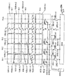
- FIG. 10 shows an example of the array of the present invention in which m photoelectric conversion cells (A1 or C1) are arranged in the first direction and n photoelectric conversion cells (A1 or C1) are arranged in the second direction.
- the number of photoelectric conversion cells in the array was m ⁇ n.
- the photoelectric conversion array is represented by 1000, and according to its position, 1000-1-1, 1000-2-1, 1000-3-1, 1000-4-1, ---, 1000-m- 1, 1000-1-2, 1000-2-2, 1000-3-2, ---, 1000-m-2, 1000-1-3, 1000-2-3, 1000-3-3,- -, 1000-m-3, ---, 1000-ij (not shown), ---, 1000-mn, and a hyphen at the end.
- 14-1, 14-2, 14-3, ---, and 14-n indicate the first selection line, and in many cases, n photoelectric conversion cells arranged in the second direction are prepared.
- Each of the first selection lines 14-1, 14-2, 14-3, ---, and 14-n is electrically connected to the first cell selection unit of the photoelectric conversion cells arranged in the same row.
- 15-1, 15-2, 15-3, ---, and 15-m indicate the first output lines, and the number m of photoelectric conversion cells arranged in the first direction is often prepared.
- Each of the first output lines 15-1, 15-2, 15-3, ---, and 15-m is connected to the first cell output unit of the photoelectric conversion cell arranged in the same column.
- the first output lines of 15-1, 15-2, 15-3, ---, 15-m are 18-1, 18-2, 18-3 when the photoelectric conversion cell A1 is changed to the photoelectric conversion cell C1.
- ---, 18-m third output line (shown in parentheses in FIG. 10).
- the photoelectric conversion cells arranged as dummy cells or the like have first selection lines 14-1, 14-2, 14-3, ---, 14-n or first output lines 15-1, 15-2, 15-3.
- ---, and 15-m may not be electrically connected, so the number of photoelectric conversion cells arranged in the second direction or the first direction does not necessarily match the number of first selection lines or the number of first output lines. .
- the selection of the address (i, j) of the photoelectric conversion array 1000 is performed by selecting one first selection line selected from the plurality of first selection lines 14-1, 14-2, 14-3, ---, 14-n. This is performed at the intersection of 14-j and one first output line 15-i selected from the plurality of first output lines 15-1, 15-2, 15-3, ---, 15-m.
- the first selection potential is supplied to the plurality of first selection lines 14-1, 14-2, 14-3, ---, 14-n,
- the second selection potential (usually pulsed) from the first selection potential to the selected first selection line 14-j, the electrical signals of the individual photoelectric conversion cells are sequentially extracted.
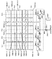
- FIG. 11 shows an example of the array of the present invention in which m photoelectric conversion cells (B1 or B2) are arranged in the first direction and n photoelectric conversion cells (B1 or B2) are arranged in the second direction.
- the number of photoelectric conversion cells in the array was m ⁇ n.
- the photoelectric conversion array is denoted by 1002, and according to its position, 1002-1-1, 1002-2-1, 1002-3-1, 1002-4-1, ---, 1002-m- 1, 1002-1-2, 1002-2-2, 1002-3-2, ---, 1002-m-2, 1002-1-3, 1002-2-3, 1002-3-3,- -, 1002-m-3, ---, 1002-ij (not shown), ---, 1002-mn, and a hyphen at the end.
- 14-1, 14-2, 14-3, ---, and 14-n indicate the first selection line, and in many cases, n photoelectric conversion cells arranged in the second direction are prepared.
- Each of the first selection lines 14-1, 14-2, 14-3, ---, and 14-n is electrically connected to the first cell selection unit of the photoelectric conversion cells arranged in the same row.
- 16-1, 16-2, 16-3, ---, 16-m indicate the second selection line, and in many cases, the number m of photoelectric conversion cells arranged in the first direction is prepared.
- the second selection lines 16-1, 16-2, 16-3, ---, and 16-m are connected to the second cell selection unit of the photoelectric conversion cells arranged in the same column.
- 17-1 and 17-2 are examples in which there are two second output lines. Electric signal outputs of two photoelectric conversion cells can be obtained simultaneously from these two second output lines 17-1 and 17-2. . For example, if selection lines connected to neighboring photoelectric conversion cells are selected at the same time, the difference between the electric signals of adjacent photoelectric conversion cells from these two second output lines 17-1 and 17-2 can be calculated in real time. Is also possible. When there is one second output line, the electric signal output from the photoelectric conversion cell can be sequentially obtained as a serial output.
- the photoelectric conversion cells arranged as dummy cells or the like include first selection lines 14-1, 14-2, 14-3, ---, 14-n, second selection lines 16-1, 16-2, 16-3. , ---, 16-m or the second output lines 17-1, 17-2 may not be electrically connected, so the number of photoelectric conversion cells arranged in the second direction or the first direction and the first selection line or It does not match the number of second selection lines.
- the selection of the address (i, j) of the photoelectric conversion array 1002 is performed by one first selection line selected from the plurality of first selection lines 14-1, 14-2, 14-3, ---, 14-n. This is performed at the intersection of 14-j and one second selection line 16-i selected from the plurality of second selection lines 16-1, 16-2, 16-3, ---, 16-m.
- the plurality of first selection lines 14-1, 14-2, 14-3, ---, 14-n, second selection lines 16-1, 16-2, 16 -3, ---, and 16-m are supplied with the first selection potential and the third selection potential, respectively, and the selected first selection line 14-j and the selected second selection line
- the second selection potential (normal pulse shape) and the fourth selection potential (normal pulse shape) from the first selection potential, the third selection potential, and the fourth selection potential (normal pulse shape) Take out sequentially.
- the photoelectric conversion element when the photoelectric conversion element is a phototransistor, a signal is not extracted from the collector but a signal is extracted from the emitter, thereby avoiding a read delay due to stray capacitance between the collector, the isolation region, and the substrate, and a delay due to the mirror effect.
- the address selection can be performed together with the current amplification by performing the address selection by the emitter.
- pixel information can be read with sensitivity close to the dark current limit.
- ⁇ Disturbance such as voltage fluctuation caused by noise and voltage fluctuations in the signal output line at the time of readout inside the readout pixel or other pixels can be suppressed by the way of connection between the selection element and the photoelectric conversion element.
- the rising noise of the address selection pulse pulse applied to the first selection line, the second selection line, or the third output line
- the noise and signal Easy to separate.
- the read signal can be cut out by strobe processing or the like to avoid the influence of noise.
- the amplification type photoelectric conversion element and the above configuration enable a photoelectric conversion cell and a two-dimensional array with high sensitivity and a large dynamic range.
- the semiconductor region in which the photoelectric conversion element is provided (the first semiconductor region in the following embodiment) is not required at least between individual photoelectric conversion cells, the semiconductor has a wavelength close to the long wavelength limit of photoelectric conversion of the semiconductor. Photoelectric conversion can be performed up to light.
- the transistor constituting the photoelectric conversion cell can also be used as a transistor that does not require an isolation structure.
- the photoelectric conversion cell and the array of the present invention can be manufactured without greatly changing the manufacturing process. For this reason, it is possible to manufacture on the MOSLSI foundry.
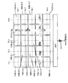
- Two-dimensional array circuit diagram with a common load resistor connected to the phototransistor collector One-dimensional array of phototransistors Other one-dimensional arrays of phototransistors
- Phototransistor cell with X-coupling wiring by capacitive coupling in the base and reading from the collector with the emitter as Y drive Other one-dimensional arrays of phototransistors
- One-dimensional array of Darlington-connected phototransistors Component connection diagram of photoelectric conversion cell A1 of the present invention
- Component connection diagram of photoelectric conversion cell B1 of the present invention Component connection diagram of photoelectric conversion cell C1 of the present invention
- Arrangement and connection diagram of photoelectric conversion arrays R1B1 and R1B2 of the present invention Sectional drawing of one of the form of the amplification type photoelectric conversion element used for the photoelectric conversion cell of this invention
- FIG. 21 shows an example of operation waveforms of the electrical signal sense control circuit.
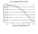
- Example of sectional view of photoelectric conversion cell A1 of the present invention Example of plan view of photoelectric conversion cell A1 of the present invention Electrical characteristics of prototype of photoelectric conversion cell A1 of the present invention (horizontal axis: first selection section voltage, vertical axis: electrical signal current obtained from first output section)
- Example of sectional view of photoelectric conversion cell B2 of the present invention Other cross-sectional examples of the photoelectric conversion cell B2 of the present invention
- Example of sectional view of photoelectric conversion cell B1 of the present invention Example of sectional view of photoelectric conversion cell C1 of the present invention
- a photoelectric conversion element to which the present invention is applied is a bipolar phototransistor.
- a desirable example of this element is: A first semiconductor region having a first surface and a first conductivity type; One or a plurality of second semiconductor regions having a second surface and a reverse conductivity type of the first conductivity type, and provided in or on the first surface of the first semiconductor region; , One or a plurality of third semiconductor regions each having a third surface and a first conductivity type, each provided in or on the second surface of the second semiconductor region; Consisting of at least When the second semiconductor region is a plurality, the second semiconductor region is electrically connected to the third semiconductor region not provided in itself except at least one, When there are a plurality of the third semiconductor region, the third semiconductor region is electrically connected to the second semiconductor region not provided with itself except at least one,
- the photoelectric conversion element BP wherein the first semiconductor region is a first electric signal output unit, and the one third semiconductor region is a second electric signal output unit.
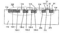
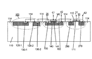
- FIG. 12 shows a cross-sectional view of a structural example and an electrical connection example of the photoelectric conversion element BP.
- 110 is the first semiconductor region
- 120-1, 120-2, ---, 120-n is the second semiconductor region
- 130-1, 130-2, ---, and 130-n are the third. It is a semiconductor region. Interconnections between the respective semiconductor regions are conceptually indicated by dotted lines, and in the illustrated example, the second semiconductor region 120-2 is a third semiconductor region 130- other than the third semiconductor region 130-2 provided thereon. Connected to one.
- the third semiconductor region 130-2 is connected to a second semiconductor region (not shown) other than the second semiconductor region 120-2 in which the third semiconductor region 130-2 is provided.
- the second semiconductor region 120-n is connected to a third semiconductor region (not shown) other than the third semiconductor region 130-n provided therein.
- the third semiconductor region 130-n also functions as a second electric signal output of the photoelectric conversion element BP.
- the semiconductor region 110 controls photoelectric conversion and simultaneously functions as a first electric signal output unit.
- the electrical signal converted from the optical information is composed of the second semiconductor regions 120-1, 120-2, ---, 120-n and the third semiconductor regions 130-1, 130-2, ---, 130-n. It is obtained with a current output in a direction in which the junction to be performed is the forward direction. In the present invention, this direction is described as “the potential difference polarity in which the second electric signal output unit easily allows the electric signal current to flow with respect to the first electric signal output unit”. Note that 114 may be provided to prevent surface leakage in a region having the same conductivity type as the first semiconductor region 110 and a higher impurity concentration.
- the photoelectric conversion element BP main photoelectric conversion is performed in the second semiconductor region and the first semiconductor region 110 that are not electrically connected to the third semiconductor region, and the junction becomes a carrier collection junction, and the first semiconductor
- the region 110 is a bipolar phototransistor and a collector of the bipolar transistor, and the second semiconductor region not electrically connected to the third semiconductor region is electrically connected to the base of the bipolar phototransistor and the third semiconductor region.
- the second semiconductor region functions as the base of the bipolar transistor
- the third semiconductor region functions as the bipolar phototransistor or the emitter of the bipolar transistor, but the device composed of the first, second, and third semiconductor regions exhibits an amplifying action. Even if not, the junction composed of the third semiconductor region and the second semiconductor region is biased when not selected. Depending on the relationship, it also acts as a blocking diode.
- the current gain of the photoelectric conversion element and the withstand voltage of the second electric signal output unit are advantageously increased by the number, but the cell area is growing.
- the number of the second and third semiconductor regions is one, it is desirable to set the transistor current gain and the junction breakdown voltage between the second and third semiconductor regions large.
- the impurity concentration of the third surface of the third semiconductor region is desirably 2E19 atoms / cc or more.
- the amplification factor of the composite transistor is the power of one transistor, and the breakdown voltage is multiple times, so the impurity concentration of the second surface of the second semiconductor region is about 1E19 atoms / cc Can be increased. Even when the current gain is small, the charge corresponding to the integrated value of the amount of light irradiated to the photoelectric conversion cell is stored in the junction between the second semiconductor region and the first semiconductor region 110 while it is not selected. Can be read.
- the impurity concentration of the surface portion of the first semiconductor region 110 is a low impurity concentration (about 1E14 to 1E17 atoms / cc), but a large impurity concentration (1E18 atoms / cc) is used to suppress back diffusion or lateral diffusion of photogenerated carriers. It is desirable to provide a region having the above on the back surface (the surface facing the first surface).
- the thickness of the low impurity concentration surface portion of the first semiconductor region 110 (the distance from the first surface to the high impurity concentration) is preferably less than the length of one side of the photoelectric conversion cell in order to suppress lateral diffusion.
- the structure of the first semiconductor region 110 improves the collection efficiency of the light-generated carriers because an electric field is formed in which the light-generated carriers are accelerated from the bottom with a high impurity concentration to the surface. Further, the movement of the light-generated carrier diving down to reach the adjacent photoelectric conversion cell is prevented. Also, the lower carrier lifetime where the impurity concentration is high is smaller than the surface portion due to the high impurity concentration, and has the function of reducing the carrier diffusion length and reducing the lateral diffusion distance of the carrier submerged in the lower portion. This configuration and countermeasure can also be applied to the photoelectric conversion element described below.
- a field effect phototransistor is a field effect phototransistor.
- a desirable example of this element is: A first semiconductor region having a first surface and a first conductivity type; A second semiconductor region having a second surface and a reverse conductivity type of the first conductivity type, provided in or on the first surface of the first semiconductor region; and A third semiconductor region having a third surface and a first conductivity type, provided in or on the second surface of the second semiconductor region; A channel formation region provided in the second semiconductor region so as to bridge between the first semiconductor region and the third semiconductor region; Consisting of at least The photoelectric conversion element FE, wherein the first semiconductor region is a first electric signal output unit, and the third semiconductor region is a second electric signal output unit.
- FIG. 13 shows a cross-sectional view of a structural example of the photoelectric conversion element FE.
- 110 is a first semiconductor region
- 120 is a second semiconductor region
- 130 is a third semiconductor region.
- 114 may be provided to prevent surface leakage in a region having the same conductivity type as the first semiconductor region 110 and a higher impurity concentration.
- Reference numeral 140 denotes a channel region 140.
- the third semiconductor region 130 also functions as a second electric signal output of the photoelectric conversion element FE.
- the first semiconductor region 110 controls photoelectric conversion and also functions as a first electric signal output unit.
- the second semiconductor region 120 functions as the gate of the field effect transistor.
- the first semiconductor region 110 and the third semiconductor region 130 function as the drain or source of the field effect transistor.
- a current flowing between the first semiconductor region 110 and the third semiconductor region 130 via the channel region 140 is controlled by the potential of the second semiconductor region 120.
- Photoelectric conversion is mainly performed in the first semiconductor region 110 and the second semiconductor region 120, and collection of photogenerated carriers is performed in the junction between the first semiconductor region 110 and the second semiconductor region 120. At the time of non-selection, photogenerated carrier charges are accumulated in the second semiconductor region 120.
- the semiconductor region 130 changes in the forward bias direction from the supplied reverse bias (the direction is important and the forward bias is not necessarily required).
- the current between the first electric signal output and the second electric signal output varies depending on the potential of the second semiconductor region 120 at the time of selection / reading. That is, the integrated value of the light amount can be read as a current.
- this photoelectric conversion element FE When this photoelectric conversion element FE is applied to the photoelectric conversion cell of the present invention, a potential difference polarity pulse in which the junction between the third semiconductor region 130 and the second semiconductor region 120 is forward is applied to the third semiconductor region 130 during reading. After that, when a pulse in the opposite direction is further applied or the third semiconductor region 130 is in a floating state (the first transistor 10 of the photoelectric conversion cell is turned off), the second semiconductor region 120 is in contact with the third semiconductor region 130. The reverse bias is set, and the accumulation of photogenerated carriers at the time of non-selection is resumed.
- the photoelectric conversion array R1A when the electrical signals read from the plurality of first output lines 15-1, 15-2, 15-3, ---, 15-m are currents, the plurality of first output lines Connect sense amplifiers to 15-1, 15-2, 15-3, ---, and 15-m, respectively, and read electrical signals in parallel.
- FIG. 14 shows an example of this.
- the output voltages of the plurality of sense amplifiers 2000-1, 2000-2, 2000-3, ---, and 2000-m are sequentially switched to the serial signal output by the switch circuit 3000. Thus, an electric signal can be taken out.
- a dark current component is obtained by providing a light-shielding film and using a value obtained by subtracting the output of the sense amplifier connected from one arbitrary first output line 15-i from the output of another sense amplifier as an electric signal. Since the electric signal obtained by subtracting the selected pulse noise component is obtained, the weak light sensitivity of the photoelectric conversion array R1A is improved.
- the first output lines 15-1, 15-2, 15-3, ---, 15-m are connected to the second output lines 17-1, 17-2, 17-3, ---, 17
- Similar effects can be obtained with other array configurations that are read as -m, third output lines 18-1, 18-2, 18-3, ---, and 18-m.
- a plurality of second output lines 17-1, 17-2, 17-3, ---, 17-m or third output lines 18-1, 18-2, 18-3, ---, 18- A light-shielding film is provided on the photoelectric conversion cell connected to any one second output line 17-i or third output line 18-i of m, and the one second output line 17-i Alternatively, a value obtained by subtracting the output of the sense amplifier connected from the third output line 18-i from the output of another sense amplifier is used as an electric signal.
- first output lines 15-1, 15-2, 15-3, ---, 15-m are voltages or charges
- the electrical signals read from the plurality of first output lines 15-1, 15-2, 15-3, ---, 15-m are voltages or charges
- a plurality of first output lines 15-1 in which one (or a plurality of (not shown) but less than the first output lines) voltage sense amplifiers 2001 are arranged in the first direction.
- 15-2, 15-3, ---, and 15-m can be sequentially switched and read.
- the first output lines 15-1, 15-2, 15-3, ---, and 15-m are sequentially connected to the sense amplifier 2001 by the switch circuit 3001, and an electric signal is output as a serial signal from the output of the sense amplifier. It can be taken out.
- the electrical signal read from the first, second, or third output line of the array of the present invention Before or after reading the electrical signal from the first, second, or third output line, It is desirable for high-precision reading to reset the first, second, or third output line to the reset potential.
- a sense amplifier having a reference input function is used as the sense amplifier, and by supplying a reference potential to the reference input, an electric signal output from each photoelectric conversion cell is obtained as a difference from a zero potential or a constant potential. be able to.
- the electrical signal output from the first, second, or third output of the photoelectric conversion cell often depends on the potential of the output.
- the electrical signal to be read is a previous history (electrical signal read before). This reset is also necessary to avoid any disturbances.
- the internal potential of the photoelectric conversion cell is reset by resetting the potential of the first, second, or third output line in the latter half of the readout time for reading the electrical signal from the first, second, or third output line. Can be reset.
- the reset potential is applied to the first and second output lines as described above (second selection potential)-the first selection potential side of Vth1, the third output. For a line, it is desirable to set a value on the first selection potential side from (second selection potential) ⁇ Vth1 ⁇ Vbe (or Vd).
- the sixth transistor is a field effect transistor having two outputs (source and drain) and a gate, One of the outputs is connected to each of the plurality of first output lines, and the other is supplied with a reset potential.
- a control voltage pulse that turns on the sixth transistor is applied to the gate
- a control potential for turning off the sixth transistor is applied to the gate, that is, At least when the first selection line transitions from the first selection potential to the second selection potential and sensing starts, a control potential for turning off the sixth transistor is applied to the gate of the sixth transistor
- the first selection potential is a potential that cuts off the electrical signal of the photoelectric conversion cell from the first cell output unit
- the second selection potential is the electrical signal current of the photoelectric conversion element compared to the first selection potential.
- a reset circuit RSA1 characterized in that the potential is in the direction of the potential difference polarity that is easy to flow.
- the sense amplifier used is preferably a sense amplifier having a reference input in addition to the electric signal input.
- the reset potential is supplied to the reference input. If the cell internal potential is only to be reset, the sixth transistor may be turned on only after the first selection line is at the second potential after reading.
- the above control voltage pulse has a potential change that drives the sixth transistor from off to on and from on to off, and at the necessary timing described above, for example, from a control pulse supply unit comprising a pulse generation circuit such as a known shift register Supplied.
- reference numeral 4010 denotes a reset circuit.
- the reset circuit 4010 includes a plurality of sixth transistors 4006-1, 4006-2, 4006-3, ---, 4006-j (j is not shown), ---, 4006-m.
- the sixth transistors 4006-1, 4006-2, 4006-3, ---, 4006-j (j is not shown), ---, 4006-m are the first output line 15-1 having the same end number. , 15-2, 15-3, ---, 15-j (j is not shown), ---, and 15-m.
- a reset potential 6001 is connected to the reference inputs 2002-1-2, 2002-2-2, 2002-2-2, ---, and 2002-m-2 of the sense amplifier.
- the control voltage pulse for turning on is at least part of the time when the first selection line potential is the first selection potential, or before the first selection line potential is at the second selection potential and changes to the first selection potential.
- Applied to the gate of the sixth transistor 4006-j (j 1, 2, 3, ---, m).
- the latter is effective for resetting the cell potential in the photoelectric conversion cell, and may be a part when the first selection line potential is at the second selection potential after the signal of the photoelectric conversion cell is read out.
- the sixth transistor 4006-j 1, 2, 3,-
- the reset potential is set to a potential on the first selection potential side of (second selection potential) ⁇ Vth1
- the convergence of the reset is fast.
- the above control voltage pulse has a potential change that drives the sixth transistor from off to on and from on to off, and at the necessary timing described above, for example, from a control pulse supply unit comprising a pulse generation circuit such as a known shift register Supplied.
- FIG. 17 is a voltage waveform example showing the operation of the reset circuit RSA1.
- This waveform is shown by the polarity when the sixth transistor is n-channel.
- the sixth transistor 4006-j 1, 2, 3, ⁇ A control pulse that turns on-and m) is applied to the gate.
- the reset circuit As a reset circuit (second mode) added to the array configuration of FIG. 15 (second mode of photoelectric conversion array R1A), It consists of multiple fourth transistors and one sixth transistor,
- the fourth transistor is a field effect transistor and has two outputs (source and drain) and a gate.
- the sixth transistor is a field effect transistor and has two outputs (source and drain) and a gate.
- One of the outputs of the plurality of fourth transistors is connected to the plurality of first output lines, and the other of the outputs of the plurality of fourth transistors is connected to a sense amplifier input.
- One output of the sixth transistor is connected to the other of the plurality of fourth transistors;
- the other output of the sixth transistor is supplied with a reset potential,
- a control voltage pulse for sequentially turning off, turning on, and turning off the plurality of fourth transistors is sequentially applied to the gates of the plurality of fourth transistors,
- a control voltage pulse that turns on the sixth transistor is applied to the gate of the sixth transistor when the fourth transistor is off or before transitioning from on to off, in other words, at least the plurality of fourth transistors
- a control potential for turning off the sixth transistor is applied to the gate of the sixth transistor at the time when the sense that one of the transistors transitions from off to on is started,
- a reset circuit RSA2 is provided.
- the sixth transistor may be turned on only while the fourth transistor is on.
- the control voltage pulse has a potential change for driving the fourth transistor or the sixth transistor from off to on, and from on to off, and is controlled by a pulse generation circuit such as a known shift register at the necessary timing described above. Supplied from the pulse supply unit.
- FIG. 4011 denotes the entire reset circuit RSA2.
- the reset circuit 4011 includes fourth transistors 4004-1, 4004-2, 4004-3, ---, 4004-m and a sixth transistor 4006-0.
- the fourth transistors 4004-1, 4004-2, 4004-3, ---, 4004-m are field effect transistors, one of two outputs (source, drain) 4004-1-1, 4004-2-1 , 4004-3-1, ---, and 4004-m-1 are connected to first output lines 15-1, 15-2, 15-3, ---, and 15-m, respectively.
- the other outputs of the fourth transistors 4004-1, 4004-2, 4004-3, ---, and 4004-m are connected to the input 2003-1 of the sense amplifier 2003.
- the sixth transistor 4006-0 is a field effect transistor, and one of the two outputs (source, drain) is one of the plurality of fourth transistors 4004-1, 4004-2, 4004-3, ---, 4004-m.
- the other of the two outputs 4006-0-2 is connected to the reset potential 6001. Note that the sense amplifier 2003 has a reference input and is connected to the reset potential.
- FIG. 19 is a voltage waveform example showing the operation of the reset circuit RSA2.
- the voltage waveforms (5) and (6) in the figure show the case where the first selection line 14-1 and then the second selection line 14-2 are driven.
- the fourth transistor 4004-j 1 , 2, 3,..., M
- a voltage pulse is sequentially applied so that the fourth transistor 4004-j is turned off ⁇ on ⁇ off.
- the electric signal of the photoelectric conversion cell at the intersection with the output line 15-j is read out. If a gate potential is applied to turn on the sixth transistor when the fourth transistor 4004-j is in an off state, the electric signal of the photoelectric conversion cell is transmitted to the input of the sense amplifier with the reset potential as a base point.
- the voltage waveform (9) further shows an operation waveform in which the sixth transistor is turned on in the second half after the fourth transistor 4004-j is turned on.
- the in-cell potential of the photoelectric conversion cell can be reset after reading the electric signal.
- the polarities of the voltage waveforms in the figure are shown with the fourth transistor 4004-j as a p-channel transistor and the sixth transistor 4006-0 as an n-channel.
- the reset circuit for the photoelectric conversion arrays R1B1 and R1B2 Consists of the sixth transistor of the following connection. Consists of a sixth transistor that is a field effect transistor having two outputs (source, drain) and gate, One of the outputs is connected to the second output line of the photoelectric conversion array R1B, the other of the outputs is given a reset potential, When the first selection line of the photoelectric conversion array R1B is the first selection potential and the second selection line is the third potential, or the second half of the first selection line transitioning to the second selection potential or the second selection line In the latter half of the transition to the fourth potential, a voltage pulse that turns on the sixth transistor is applied to the gate.
- the second selection line is at the fourth selection potential and the first selection line is the first.
- a control potential at which the sixth transistor is turned off is applied to the gate of the six transistors
- the first selection potential is a potential that cuts off the electrical signal of the photoelectric conversion cell from the second cell output unit
- the second selection potential is an electric signal current of the photoelectric conversion element as compared to the first selection potential.
- the reset circuit RSB1 wherein the third selection potential is a potential that cuts off the second transistor, and the fourth selection potential is a potential in a direction that makes the second transistor conductive. Note that if it is only for resetting the cell internal potential, after reading, the sixth transistor is turned on only while the first selection line is at the second selection potential and the second selection line is at the fourth potential. You can do it.
- reference numeral 4020 denotes a reset circuit RSB1.
- the reset circuit 4020 includes a sixth transistor 4006-0.
- the sixth transistor 4006-0 is a field effect transistor, and one output 4006-0-1 of the two outputs (source or drain) of the sixth transistor 4006-0 is connected to the second output line 17,
- the other 4006-0-2 is connected to the reset potential 6001.
- the input 2002-0-1 of the sense amplifier 2002 is connected to the second output line 17 and one output 4006-0-1 of the sixth transistor.
- a reset potential 6001 is connected to the reference input 2002-0-2 of the sense amplifier 2002.
- a control voltage pulse for turning on and off the sixth transistor is applied to the gate 4006-0-3 of the sixth transistor.
- the control voltage pulse for turning on is at least part of the time when the first selection line potential is the first selection potential and the second selection line potential is the third selection potential, or the first selection line potential is the second selection.
- the voltage is applied to the gate of the sixth transistor before the transition to the first selection potential or before the transition of the second selection line potential to the fourth selection potential and the transition to the third third selection potential. The latter is effective for resetting the cell potential in the photoelectric conversion cell.
- the above control voltage pulse has a potential change that drives the sixth transistor from off to on and from on to off, and at the necessary timing described above, for example, from a control pulse supply unit comprising a pulse generation circuit such as a known shift register Supplied.
- a third output line 18 is connected to the third output line 18 by supplying a fifth output potential to the third output line 18.
- the electric signal may be any of current, charge and voltage.
- the sense amplifier 2002 preferably has a reference input terminal in addition to the electric signal input terminal.
- the sixth potential is supplied to the reference input terminal.
- current sensing current sensing is performed in the vicinity of the potential. Set to do.
- the sixth potential can also be used as the reset potential.
- the signal voltage is sensed as a difference from the potential.
- charge sensing the charge accumulated at the sense amplifier input is charged by the input capacitance of the sense amplifier 2002, the floating capacitance of the third output line 18-j, and the floating capacitance of the signal path of the electrical signal sense control circuit 4030. The voltage converted voltage is sensed as a change from the sixth potential.
- the electric signal is read by sequentially driving the circuit to the second selection potential.
- the electric signal sense control circuit 4030 drives the third output line 18-j to the sixth potential, thereby The cell potential in the conversion cell C1 can be reset.
- 1) and 2) may be interchanged.
- this electric signal sense control circuit 4030 can also be applied to the array R1A composed of the photoelectric conversion cells A1. In the above description, the same operation can be described by replacing the third output line 18-j with the first output line 15-j.
- the electrical signal sense control circuit has the following configuration.
- a connection circuit; An output non-selection potential setting circuit; An output selection potential setting circuit; Consists of The connection circuit is provided between the plurality of third output lines of the photoelectric conversion array R1C and the input of the sense amplifier, The connection circuit has a low resistance between one third output line selected from the plurality of third output lines and the input of the sense amplifier, and a high resistance between the other third output line and the input of the sense amplifier.
- the output non-selection potential setting circuit is provided between the plurality of third output lines and the fifth potential supply means, The output non-selection potential setting circuit has a high resistance between the third output line selected from the plurality of third output lines and the fifth potential supply means, and supplies the fifth potential to the unselected third output line,
- the output selection potential setting circuit is provided between the sense amplifier side of the connection circuit (input of the sense amplifier) and the sixth potential supply means, The output selection potential setting circuit is at least partially when the plurality of first selection lines of the photoelectric conversion array R1C are all at the first selection potential, or one of the plurality of first selection lines is second selected.
- the sixth potential is supplied to the sense amplifier side (input of the sense amplifier) of the connection circuit before transitioning to the first selection potential, and the resistance becomes high at other points of time, that is, the output At least the selection potential setting circuit has a high resistance when one of the plurality of first selection lines of the photoelectric conversion array R1C transitions from the first selection potential to the second selection potential,
- the first selection potential is a potential that cuts off the electric signal of the photoelectric conversion cell from the third cell output unit
- the second selection potential is an electric signal current of the photoelectric conversion element as compared with the first selection potential.
- An electric signal sense control circuit wherein the electric signal sense control circuit is a potential in a direction of a potential difference polarity that easily flows. In this case, it is desirable that the sense amplifier has a reference input in addition to the input and output, and the sixth potential is supplied to the reference input.
- This electrical signal sense control circuit replaces the third output line with the first output line and applies it to the photoelectric conversion array R1A, thereby avoiding the need for parallel reading of the photoelectric conversion cell A1. That is, A connection circuit; An output non-selection potential setting circuit; An output selection potential setting circuit; Consists of The connection circuit is provided between the plurality of first output lines of the photoelectric conversion array R1A and the input of the sense amplifier, The connection circuit has a low resistance between one first output line selected from the plurality of first output lines and the input of the sense amplifier, and a high resistance between the other first output line and the input of the sense amplifier.
- the output non-selection potential setting circuit is provided between the plurality of first output lines and the fifth potential supply means, The output non-selection potential setting circuit has a high resistance between the third output line selected from the plurality of first output lines and the fifth potential supply means, and supplies the fifth potential to the unselected first output line,
- the output selection potential setting circuit is provided between the input of the sense amplifier (sense amplifier side of the connection circuit) and the sixth potential supply means, The output selection potential setting circuit has at least a part when the plurality of first selection lines of the array R1A are all at the first selection potential, or one of the plurality of first selection lines is at the second selection potential.
- the sixth potential is supplied to the input of the sense amplifier (the sense amplifier side of the connection circuit) and becomes a high resistance at other times, that is, the output selection potential setting circuit At least, when one of the plurality of first selection lines of the photoelectric conversion array transitions from the first selection potential to the second selection potential, the resistance becomes high.
- the first selection potential is a potential that cuts off the electrical signal of the photoelectric conversion cell from the first cell output unit
- the second selection potential is the electrical signal current of the photoelectric conversion element compared to the first selection potential.
- An electric signal sense control circuit wherein the electric signal sense control circuit is a potential in a direction of a potential difference polarity that easily flows.
- connection circuit is composed of a plurality of fourth transistors,
- the plurality of fourth transistors are field effect transistors and have two output portions (source and drain), and one of the output portions is connected to the plurality of third output lines or the plurality of first output lines, respectively.
- the output non-selection potential setting circuit is composed of a plurality of fifth transistors, The plurality of fifth transistors have two output units, one of the output units is connected to the plurality of third output lines, respectively, the other of the output units is connected to the fifth potential supply means,
- the output selection potential setting circuit is composed of a sixth transistor, The sixth transistor is a field effect transistor and has two output portions (source and drain), one of the output portions is connected to the sixth potential supply means, and the other of the output portions is the plurality of fourth outputs. Connected to the other output of the transistor, The electrical signal sense control circuit characterized by the above.
- FIG. 21 shows one mode of this electric signal sense control circuit.
- reference numeral 4030 denotes the entire electric signal sense control circuit.
- 4004-1, 4004-2, 4004-3, ---, 4004-m are the third output lines 18-1, 18-2, 18-3, --- 18, m of the photoelectric conversion array R1C.
- a plurality of fourth transistors 4004-1, 4004-2, 4004-3, ---, and 4004-m for connecting and disconnecting the sense amplifier 2002 in time series form a connection circuit 4034.
- the plurality of fourth transistors 4004-1, 4004-2, 4004-3, ---, 4004-m are field effect transistors, and one of the two output portions (source, drain) is a plurality of third transistors of the array.
- 4005-1, 4005-2, 4005-3, ---, 4005-m are a plurality of third output lines 18-1, 18-2, 18-3, --- 18-m of the photoelectric conversion array R1C.
- One of the two output parts (source, drain or emitter, collector) of the plurality of fifth transistors 4005-1, 4005-2, 4005-3, ---, 4005-m is a plurality of the second transistors of the photoelectric conversion array R1C.
- Pulses for controlling on / off of 4005-m in time series are connected to the gates of the fourth transistors 4004-1, 4004-2, 4004-3, ---, and 4004-m, respectively.
- 4th transistor 4004-1, 4004-2, 4004-3, ---, 4004-m and 5th transistor 4005-1, 4005-2, 4005-3, ---, 4005-m 4004-1 And 4005-1, 4004-2 and 4005-2, 4004-3 and 4005-3, ---, 4004-m and 4005-m are complementary transistors, respectively.
- the control pulses applied to the base are reduced from two to one.
- the sixth transistor 4006-0 constitutes an output selection potential setting circuit 4036 and is a field effect transistor, and one of its two outputs (source and drain) is connected to the sixth through the terminal 4032-6 of the electric signal sense control circuit 4030.
- An electric signal sense control circuit connected to the potential supply means 6003 and the other connected to the other output of the plurality of fourth transistors 4004-1, 4004-2, 4004-3, ---, 4004-m It is connected to the input 2002-1 of the sense amplifier 2002 via the terminal 4032-0 of 4030.
- the sixth transistor 4006-0 is controlled to be turned on in at least a part of the phase in which the photoelectric conversion cell C1 is not selected by a control pulse given to the gate via the terminal 4033-63.
- the phase in which the photoelectric conversion cell C1 is not selected is that all the first selection lines 14-1, 14-2, 14-3, ---, and 14-n of the photoelectric conversion array R1C are at the first potential.
- the phase in which the photoelectric conversion cell C1 is selected is one of the first selection lines 14-1, 14-2, 14-3, ---, and 14-n of the photoelectric conversion array R1C. This is a potential phase.
- the sense amplifier 2002 preferably has a reference potential input 2002-2 in addition to the signal input 2002-1.
- the reference potential input 2002-2 is supplied with the sixth potential from the sixth potential supply means 6003.
- the signal input is sensed in the vicinity of the sixth potential.
- the difference from this sixth potential is sense amplified and output. Therefore, it is desirable that the electric signal sense control circuit 4030 has a function of resetting the input of the sense amplifier to the sixth potential in a phase where there is no signal input.
- the internal potential of the photoelectric conversion cell C1 can be reset following the reading by turning it on from off. In this case, in order to converge reset more quickly, as described above, the sixth potential supply means 6003 is set to a value on the first selection potential side from (second selection potential) -Vth1-Vbe (or Vd). It is desirable to do.
- Each terminal of the electric signal sense control circuit 4030, the terminal of the sense amplifier 2002, the terminal of the fifth potential supply means 5003, and the terminal of the sixth potential supply means 6003 are integrated on the same chip as the photoelectric conversion array R1C and the like. In this case, there is no shape as a terminal, and each part and each block are provided in a form connected by a continuous conductive thin film.
- the terminals described here are convenient names for representing the divisions for each functional block, and there are many cases where there is no actual situation. It is a connection point on the circuit diagram.
- the fifth potential supply means 5003 or the sixth potential supply means 6003 may be a wiring that supplies the fifth potential or the sixth potential from an external pad, or a power source that supplies the fifth potential or the sixth potential. It may be a circuit.
- FIG. 22 shows an example of voltage waveforms related to the electric signal sense control circuit 4030 whose circuit diagram is shown in FIG.
- the polarity of the voltage waveform is the fourth transistor 4004-1, 4004-2, 4004-3, ---, 4004-m is the p-channel field effect transistor, the fifth transistor 4005-1, 4005-2, 4005-3,- -And 4005-m are p-channel field effect transistors, and the sixth transistor 4006-0 is an n-channel field effect transistor.
- the first transistor 10 of the photoelectric conversion cell C1 is a p-channel field effect transistor.
- Waveforms (1), (2), (3), (4) are multiple fifth transistor fourth transistor pairs (4005-1, 4004-1), (4005-2, 4004-2), --- The voltage pulses applied to the gates for on / off control of the.
- Waveform (1) is a voltage waveform applied to the gate (via terminal 4033-1) to drive the fourth transistor 4004-1 from OFF to ON
- Waveform (2) is a voltage waveform applied to the gate of the fifth transistor 4005-1 via the terminal 4033-01 in order to drive the fifth transistor 4005-1 from on to off.
- Waveforms (1) and (2) are given in time series to ensure a phase in which both transistors are off before either the fourth or fifth transistor is turned on.
- the fourth transistor 4004-1 is turned on in waveform (1), and then the fourth transistor 4004-1 is turned off.
- the fifth transistor 4005-1 is turned on.
- a sixth transistor 4006 having one of its outputs connected to the sixth potential supply means 6003 so that the sixth potential is supplied to the third output line 18-1 when the fourth transistor 4004-1 is turned on. -0 is on.
- a voltage pulse indicated by waveform (9) is supplied to the gate of the sixth transistor 4006-0 (via the terminal 4033-63).
- the first selection lines 14-1, 14-2, 14-3, ---, and 14-n have waveforms (5), (6), (7 ) And (8), the first selection potential, the second selection potential, and the first selection potential are sequentially driven. Accordingly, the third output line 18-1 ⁇ the terminal 4030-1 ⁇ the one output of the fourth transistor 4004-1 ⁇ the other output ⁇ the terminal 4032 and the third output line 18-1 and the first selection lines 14-1 , 14-2, 14-3, --- 14-n
- the electrical signals of the photoelectric conversion cell C1 located at the intersections are sequentially read out and sequentially input to the sense amplifier via the sense amplifier input terminal 2003-1.
- the Waveform (10) is the voltage waveform of third output line 18-1 (terminal 4030-1 connected thereto) at this time, and waveform (12) is the waveform of sense amplifier input 2002-1 at this time Yes (also the waveform of terminal 4032-0).
- a broken-line circle in the drawing indicates a time phase in which an electric signal is sensed.
- the fifth potential of the waveform (10), that is, the waveform of the third output line 18-1, is not transmitted to the sense amplifier input because the fourth transistor 4004-1 is off.
- the first selection lines 14-1, 14-2, 14-3, --- 14-n are By sequentially driving from one selection potential to the second selection potential and further to the first selection potential, a third output line 18-j (not shown) and each first selection line 14-1, 14-2, 14- 3.
- the electrical signal of the photoelectric conversion cell C1 located at the intersection with --14-n is sequentially read out.
- the sixth transistor when the electric signal is not read (when the potentials of all the first selection lines 14-1, 14-2, 14-3, and --14-n are the first selection potential)
- the sense circuit input can be reset to the sixth potential during the time during which the electrical signal is read, so the output of the sense amplifier 2002 supplied with the sixth potential to the reference potential input 2002-2 is In the time when there is no electric signal input, it operates at zero or constant potential.
- the phase after any of the first selection lines 14-1, 14-2, 14-3, --- 14-n is the second selection potential and the electric signal is read
- the sixth transistor 4006-0 the cell internal potential of the photoelectric conversion cell C1 selected at that time can be reset.
- the sixth potential by setting the sixth potential to a value on the first selection potential side from (second selection potential) ⁇ Vth1 ⁇ Vbe (or Vd), the cell internal potential can be converged at higher speed.
- a structural example A1str of the photoelectric conversion cell A1 of the present invention is as follows. That is, A first semiconductor region having a first surface and a first conductivity type; One or a plurality of second semiconductor regions having a second surface and a reverse conductivity type of the first conductivity type, and provided in or on the first surface of the first semiconductor region; , One or a plurality of third semiconductor regions each having a third surface and a first conductivity type, each provided in or on the second surface of the second semiconductor region; A seventh surface having a seventh surface and a reverse conductivity type of the first conductivity type, and provided in the first surface of the first semiconductor region or on the first surface so as to be separated from the second semiconductor region; A semiconductor region; Having an opposite conductivity type to the eighth surface, in the first surface of the first semiconductor region or on the first surface, spaced apart from the second and seventh semiconductor regions and the seventh semiconductor region and the second semiconductor region An eighth semiconductor region provided facing the surface direction; A first gate insulating film provided on at least a portion of the first
- the third semiconductor region is electrically connected to the second semiconductor region that is not provided by itself except for one;
- the second semiconductor region that is not electrically connected to the third semiconductor region forms a main photoelectric conversion junction with the first semiconductor region,
- the one third semiconductor region that is not connected to the second semiconductor region is electrically connected to the seventh semiconductor region;
- the eighth semiconductor region constitutes the first cell output portion of the photoelectric conversion cell,
- FIG. 23 shows a sectional view of a structural example and electrical connection example of the photoelectric conversion cell A1str.
- 110 is a first semiconductor region
- 120-1, 120-2 and 120-3 are second semiconductor regions
- 130-1, 130-2 and 130-3 are third semiconductor regions.
- the first semiconductor region 110, the second semiconductor regions 120-1, 120-2, 120-3, and the third semiconductor regions 130-1, 130-2, 130-3 constitute the photoelectric conversion element 100 of the photoelectric conversion cell.
- Interconnections between the respective semiconductor regions are conceptually indicated by dotted lines, and in the illustrated example, the second semiconductor region 120-2 is a third semiconductor region 130- other than the third semiconductor region 130-2 provided thereon. Connected to one.
- the second semiconductor region 120-3 is connected to a third semiconductor region 130-2 other than the third semiconductor region 130-3 provided therein.
- the third semiconductor region 130-3 is connected to the eighth semiconductor region 280.
- the seventh semiconductor region 270 constitutes a first cell output unit of the photoelectric conversion cell A1.
- 61 schematically shows the connection to the first output line 15 in the case of constituting the photoelectric conversion array R1A.
- the first gate 112 is formed on the portion of the first surface of the first semiconductor region 110 sandwiched between the seventh and eighth semiconductor regions 270 and 280 and on the surfaces of the seventh and eighth semiconductor regions 270 and 280 adjacent thereto.
- the first gate 112 constitutes a first cell selection unit of the photoelectric conversion cell A1. 31 schematically shows connection to the first selection line 14 in the case of constituting the photoelectric conversion array R1A.
- the first semiconductor region 110 having the structure of FIG. 23 can be n-type or p-type, but the following combination example is possible when the structure of FIG. 24 is realized by a silicon semiconductor as one embodiment.
- the first semiconductor region 110 is a 1 to 10 ⁇ cm n-type silicon substrate. It can also be implemented as a high-resistance n-type epitaxial layer (10 to 20 ⁇ m thick) on a low-resistance n-type Si substrate with the aim of improving long-wavelength photosensitivity, preventing optical information mixing between adjacent cells, and preventing noise. .
- the second semiconductor regions 120-1, 120-2, 120-3 are p-type silicon having a surface impurity concentration of 1E18 to 1E19 (atoms / cm 3 ),
- the third semiconductor regions 130-1, 130-2, 130-3 are shallower than the second semiconductor regions 120-1, 120-2, 120-3 in which the depths are accommodated, respectively, and the surface impurity concentrations are respectively 1E19 to 1E21 (atoms / cm 3 ) n-type silicon larger than the second semiconductor regions 120-1, 120-2, 120-3 that are housed
- the seventh and eighth semiconductor regions 270 and 280 are formed of p-type silicon having a surface impurity concentration of 1E19 to 1E20 (atoms / cm 3 ).
- the first insulating film 111 is a silicon oxide film having a thickness of 30 to 40 nm, and the first gate 112 is p-type polycrystalline silicon.
- FIG. 24 shows a plan view example of the photoelectric conversion cell A1str.
- the same numerical symbols as in FIG. 23 have the same cross-sectional structure and perform the same function. Note that the surface of the first semiconductor region 110 shown in the figure is covered with the semiconductor region 114 in order to prevent surface leakage current.
- Contact holes not shown in FIG. 23 are also shown in FIG. 24, and 123-2 and 123-3 are wirings drilled in insulating films provided on the second semiconductor regions 120-2 and 120-3, respectively.
- the contact holes 133-1, 133-2, and 133-3 are contact holes for wiring drilled in the insulating films provided on the third semiconductor regions 130-1, 130-2, and 130-3, respectively. is there.
- FIG. 24 the interconnections schematically indicated by dotted lines in FIG. 23 are shown in plan view, but the numbering is omitted. Note that the dimensions (channel width) of the seventh and eighth semiconductor regions 270 and 280 along the longitudinal direction of the first gate 112 are set larger than the example of FIG. 25 in order to increase the electric signal reading speed or reset speed of the cell. be able to.
- 14-k is the first selection line 14 when configuring the array
- 15-j is the first output line 15 when configuring the array.
- FIG. 25 shows the photoelectric conversion cell A1str shown in FIG. 24 in a CMOS-based manufacturing process.
- the dose and drive-in of one step of ion implantation and diffusion steps are performed.
- the voltage-current characteristic of the 1st cell output part at the time of the weak light irradiation of photoelectric conversion cell A1str produced by changing temperature and time is shown. It has been confirmed that a current about 380,000 times the photocurrent of the photodiode formed by the second semiconductor region 120-1 and the first semiconductor region 110 is obtained from the first cell output portion.
- the first selection potential is set to Vcc (5 V), and the second selection potential is set to Vss (0 V).
- the current from the photoelectric conversion cell A1str is cut off until the potential of the first cell selection unit is about 0.5 V less than the second selection potential.
- the dark current of the photoelectric conversion cell A1str is 1E-11A level.
- the lighting used in this experiment is orders of magnitude darker than the room lighting level, so the output current increases by an order of magnitude if the value in FIG. Therefore, the photoelectric conversion cell A1str of the present invention can have a dynamic range of 7 digits.
- the upper limit of the output current is determined by the channel width of the first transistor 10.
- Vout1 is the first cell output unit voltage
- the vertical axis Iout1 is the read DC current from the first cell output unit when the first cell output unit voltage Vout1 is 0 V
- Vselectp1 Is the first cell selector voltage.
- These voltages are expressed as voltages of the first cell output unit and the first cell selection unit, respectively, based on one power supply potential Vss (fixed to 0 V in the measurement) of the photoelectric conversion cell.
- the other power supply potential Vcc used for this measurement is Vss + 5V.
- a structural example B2str of the photoelectric conversion cell B2 of the present invention is as follows. That is, A first semiconductor region having a first surface and a first conductivity type; One or a plurality of second semiconductor regions having a second surface and a reverse conductivity type of the first conductivity type, and provided in or on the first surface of the first semiconductor region; , One or a plurality of third semiconductor regions each having a third surface and a first conductivity type, each provided in or on the second surface of the second semiconductor region; A fourth surface having a reverse conductivity type and a fourth surface, and provided in the first surface of the first semiconductor region or on the first surface so as to be separated from the one or more second semiconductor regions.
- a seventh semiconductor region The seventh semiconductor region having a conductivity type opposite to that of the eighth surface, spaced apart from the second, fourth, and seventh semiconductor regions in or on the first surface of the first semiconductor region And an eighth semiconductor region provided facing the first surface direction, On the first gate insulating film and the first gate insulating film provided at least in part in or on the first surface sandwiched between the seventh semiconductor region and the eighth semiconductor region A first gate provided to bridge the seventh semiconductor region and the eighth semiconductor region; Consisting of at least The third semiconductor region is electrically connected to the second semiconductor region that is not provided by itself except for one; The second semiconductor region that is not electrically connected to the third semiconductor region forms a main photoelectric conversion junction with the first semiconductor region, The one third semiconductor region that is not connected to the second semiconductor region is electrically connected to the fifth semiconductor region; The sixth semiconductor region and the eighth semiconductor region are electrically connected; The seventh semiconductor region constitutes the second cell output part of the photoelectric conversion cell, The photoelectric conversion cell B2str, wherein the first gate constitutes a first cell selection unit, and
- the fourth semiconductor region and the seventh semiconductor region can be formed continuously.
- the seventh semiconductor region and the fifth semiconductor region can be brought into contact with each other at an impurity concentration portion of 2E19 atoms / cc or more so as to be electrically connected to each other.
- the state in which the two regions are “electrically connected” indicates that the two regions are connected with a resistance value that does not hinder the operation.
- a conductive film is provided on the insulating film also serving as a passivation provided on the two regions, and the surface of the two regions via two contact holes provided on the insulating film on the two regions. This is realized by bringing the conductive film into contact with the inside or on the surface. However, when there is no contact hole and the conductive film capacitively couples the two regions via the insulating film, it is electrically connected in an alternating current manner.
- FIG. 26 shows a cross-sectional view of this photoelectric conversion cell structure example and electrical connection example B2str.
- 110 is a first semiconductor region
- 120-1 and 120-2 are second semiconductor regions
- 130-1 and 130-2 are third semiconductor regions.
- the first semiconductor region 110, the second semiconductor regions 120-1 and 120-2, and the third semiconductor regions 130-1 and 130-2 constitute the photoelectric conversion element 100 of the photoelectric conversion cell B2.
- 270 and 280 are seventh and eighth semiconductor regions
- 111 and 112 are a first insulating film, and a first gate provided on the first insulating film.
- the first gate 112 is formed on the portion of the first surface of the first semiconductor region 110 sandwiched between the seventh and eighth semiconductor regions 270 and 280 and on the surfaces of the seventh and eighth semiconductor regions 270 and 280 adjacent thereto. Through the first insulating film 111, a channel is induced and extinguished in the first surface of the first semiconductor region 110 between the seventh and eighth semiconductor regions 270 and 280 or on the first surface by the potential change.
- the first transistor 10 includes the first surface of the first semiconductor region 110 sandwiched between the seventh and eighth semiconductor regions 270 and 280, the seventh and eighth semiconductor regions 270 and 280, the first insulating film 111, and the first gate 112. Configure.
- 140, 150, and 160 are the fourth, fifth, and sixth semiconductor regions
- 141 is the fourth insulating film provided on the fourth surface of the fourth semiconductor region
- 142 is provided on the fourth insulating film.
- the fourth gate 142 is formed on the portion of the fourth surface of the fourth semiconductor region 140 sandwiched between the fifth and sixth semiconductor regions 150 and 160 and on the surface of the adjacent fifth and sixth semiconductor regions 150 and 160.
- the second transistor 20 is formed by the fourth surface of the fourth semiconductor region sandwiched between the fifth and sixth semiconductor regions 150 and 160, the fifth and sixth semiconductor regions 150 and 160, the fourth insulating film 141, and the fourth gate 142.
- the second semiconductor region 120-2 is a third semiconductor region 130- other than the third semiconductor region 130-2 provided thereon. Connected to one.
- the third semiconductor region 130-2 is connected to the fifth semiconductor region 150.
- the sixth semiconductor region 160 is connected to the eighth semiconductor region 280.
- the seventh semiconductor region 270 constitutes the second cell output of the photoelectric conversion cell B2.
- 62 schematically shows connection to the second output line 17 in the case of constituting the photoelectric conversion array R1B2.
- the first gate 112 constitutes a first cell selection unit of the photoelectric conversion cell B2.
- 31 schematically shows connection to the first selection line 14 in the case of constituting the photoelectric conversion array R1B2.
- the fourth gate 142 constitutes a second cell selection unit of the photoelectric conversion cell B2.
- 41 schematically shows connection to the second selection line 16 in the case of constituting the photoelectric conversion array R1B2.
- Reference numeral 42 schematically shows the connection of the fourth semiconductor region 140 to the fourth bias potential.
- FIG. 27 is a cross-sectional view in the case where the fourth semiconductor region 140 and the eighth semiconductor region 280 are in contact with each other in the cross-sectional view of the structural example and the electrical connection example of the photoelectric conversion cell B2str in FIG.
- the fourth bias potential wiring to the fourth semiconductor region 140 becomes unnecessary, and the area required between the fourth semiconductor region 140 and the eighth semiconductor region 280 can be reduced, and the photoelectric conversion cell B2str area can be reduced.
- the sixth semiconductor region 160 and the eighth semiconductor region 280 can be brought into contact with each other, and the area can be further reduced.
- the impurity concentration at the contact portion of the sixth semiconductor region 160 and the eighth semiconductor region 280 is 2E19 atoms / cc or more, the contact resistance is reduced and the interconnection by the metal thin film (schematically shown by dotted lines in the figure) ) Becomes unnecessary.
- a structural example B1str of the photoelectric conversion cell B1 of the present invention is as follows. That is, A first semiconductor region having a first surface and a first conductivity type; One or a plurality of second semiconductor regions having a second surface and a reverse conductivity type of the first conductivity type, and provided in or on the first surface of the first semiconductor region; , One or a plurality of third semiconductor regions each having a third surface and a first conductivity type, each provided in or on the second surface of the second semiconductor region; A seventh surface having a seventh surface and a reverse conductivity type of the first conductivity type, and provided in the first surface of the first semiconductor region or on the first surface so as to be separated from the second semiconductor region; A semiconductor region; The first surface has a conductivity type opposite to that of the eighth surface, and is separated from the second and seventh semiconductor regions in the first surface of the first semiconductor region or on the first surface and faces the seventh semiconductor region.
- An eighth semiconductor region a first gate insulating film provided on at least a portion of the first surface sandwiched between the seventh semiconductor region and the eighth semiconductor region, and the first gate insulating film A first gate provided so as to bridge the seventh semiconductor region and the eighth semiconductor region; A ninth surface and a reverse conductivity type of the first conductivity type, separated from the second, seventh, and eighth semiconductor regions in or on the first surface of the first semiconductor region; A ninth semiconductor region provided, and The ninth semiconductor region has a conductivity type opposite to that of the tenth surface, is spaced apart from the second, eighth, and ninth semiconductor regions in or on the first surface of the first semiconductor region.
- a tenth semiconductor region provided opposite to, A second gate insulating film provided on at least a portion of the first surface sandwiched between the ninth semiconductor region and the tenth semiconductor region; and the ninth semiconductor region and the second gate insulating film on the second gate insulating film.
- the third semiconductor region is electrically connected to the second semiconductor region that is not provided by itself,
- the second semiconductor region that is not electrically connected to the third semiconductor region forms a main photoelectric conversion junction with the first semiconductor region,
- the one third semiconductor region that is not connected to the second semiconductor region is electrically connected to the eighth semiconductor region;
- the seventh semiconductor region and the tenth semiconductor region are electrically connected;
- the ninth semiconductor region constitutes the second cell output part of the photoelectric conversion cell,
- the photoelectric conversion cell B1str wherein the first gate constitutes a first cell selection unit, and the second gate constitutes a second cell selection unit.
- FIG. 28 shows a sectional view of a structural example and electrical connection example of the photoelectric conversion cell B1str.
- 110 is a first semiconductor region
- 120-1 and 120-2 are second semiconductor regions
- 130-1 and 130-2 are third semiconductor regions.
- the first semiconductor region 110, the second semiconductor regions 120-1 and 120-2, and the third semiconductor regions 130-1 and 130-2 constitute the photoelectric conversion element 100 of the photoelectric conversion cell B1.
- 270 and 280 are seventh and eighth semiconductor regions
- 111 and 112 are a first insulating film, and a first gate provided on the first insulating film.
- the first gate 112 is formed on the portion of the first surface of the first semiconductor region 110 sandwiched between the seventh and eighth semiconductor regions 270 and 280 and on the surfaces of the seventh and eighth semiconductor regions 270 and 280 adjacent thereto. Through the first insulating film 111, a channel is induced and extinguished in the first surface of the first semiconductor region 110 between the seventh and eighth semiconductor regions 270 and 280 or on the first surface by the potential change.
- the first transistor 10 includes the first surface of the first semiconductor region 110 sandwiched between the seventh and eighth semiconductor regions 270 and 280, the seventh and eighth semiconductor regions 270 and 280, the first insulating film 111, and the first gate 112. Configure.
- 290 and 300 are the ninth and tenth semiconductor regions
- 121 is the second insulating film provided on the first surface of the first semiconductor region
- 122 is the second gate provided on the second insulating film. is there.
- the second gate 122 is formed on the portion of the first surface of the first semiconductor region 110 sandwiched between the ninth and tenth semiconductor regions 290 and 300 and on the surface of the adjacent ninth and tenth semiconductor regions 290 and 300.
- a channel is induced and extinguished in or on the first surface of the first semiconductor region 110 between the ninth and tenth semiconductor regions 290 and 300 by the potential change.
- the second transistor 20 is formed by the first surface of the first semiconductor region 110 sandwiched between the ninth and tenth semiconductor regions 290 and 300, the ninth and tenth semiconductor regions 290 and 300, the second insulating film 121, and the second gate 122. Configure.
- the second semiconductor region 120-2 is a third semiconductor region 130- other than the third semiconductor region 130-2 provided thereon. Connected to one.
- the third semiconductor region 130-2 is connected to the eighth semiconductor region 280.
- the seventh semiconductor region 270 is connected to the tenth semiconductor region 300.
- the ninth semiconductor region 290 constitutes the second cell output portion of the photoelectric conversion cell B1.
- 62 schematically shows the connection to the second output line 17 in the case of constituting the photoelectric conversion array R1B1.
- the first gate 112 constitutes a first cell selection unit of the photoelectric conversion cell B1.
- 31 schematically shows the connection to the first selection line 14 in the case of constituting the photoelectric conversion array R1B1.
- the second gate 122 constitutes a second cell selection unit of the photoelectric conversion cell B1.
- 41 schematically shows connection to the second selection line 16 in the case of constituting the photoelectric conversion array R1B1. Note that the seventh semiconductor region 270 and the tenth semiconductor region 300 are in contact with each other without being separated from each other, so that the area of the photoelectric conversion cell B1 can be reduced.
- a structural example C1str of the photoelectric conversion cell C1 of the present invention is as follows. That is, A first semiconductor region having a first surface and a first conductivity type; One or a plurality of second semiconductor regions having a second surface and a reverse conductivity type of the first conductivity type, and provided in or on the first surface of the first semiconductor region; , One or a plurality of third semiconductor regions each having a third surface and a first conductivity type, each provided in or on the second surface of the second semiconductor region; An eleventh surface and an opposite conductivity type, and are provided in the first surface of the first semiconductor region or on the first surface and spaced apart from the one or more second semiconductor regions.
- An eighth semiconductor region spaced from the semiconductor region and provided opposite to the seventh semiconductor region and the first surface direction; On the first gate insulating film and the first gate insulating film provided at least partly in or on the first surface sandwiched between the seventh semiconductor region and the eighth semiconductor region A first gate provided to bridge the seventh semiconductor region and the eighth semiconductor region; Consisting of at least The second semiconductor region is electrically connected to the third semiconductor region that is not provided in itself except at least one; The third semiconductor region is electrically connected to the second semiconductor region that is not provided by itself except at least one; The third semiconductor region is electrically connected to the eighth semiconductor region; The seventh semiconductor region is electrically connected to the eleventh semiconductor region; The first gate constitutes a first cell 1 selection unit, The photoelectric conversion cell C1str, wherein the twelfth semiconductor region constitutes a third cell output unit.
- the cell area can be reduced by arranging the seventh semiconductor region and the eleventh semiconductor region in contact with each other.
- FIG. 29 shows a sectional view of a structural example and an electrical connection example of the photoelectric conversion cell C1str.
- 110 is a first semiconductor region
- 120-1 and 120-2 are second semiconductor regions
- 130-1 and 130-2 are third semiconductor regions.
- the first semiconductor region 110, the second semiconductor regions 120-1 and 120-2, and the third semiconductor regions 130-1 and 130-2 constitute the photoelectric conversion element 100 of the photoelectric conversion cell C1.
- 270 and 280 are seventh and eighth semiconductor regions
- 111 and 112 are a first insulating film, and a first gate provided on the first insulating film.
- the first gate 112 is formed on the portion of the first surface of the first semiconductor region 110 sandwiched between the seventh and eighth semiconductor regions 270 and 280 and on the surfaces of the seventh and eighth semiconductor regions 270 and 280 adjacent thereto. Through the first insulating film 111, a channel is induced and extinguished in the first surface of the first semiconductor region 110 between the seventh and eighth semiconductor regions 270 and 280 or on the first surface by the potential change.
- the first transistor 10 includes the first surface of the first semiconductor region 110 sandwiched between the seventh and eighth semiconductor regions 270 and 280, the seventh and eighth semiconductor regions 270 and 280, the first insulating film 111, and the first gate 112.
- Configure. 310 and 320 are the eleventh and twelfth semiconductor regions 310 and 320, respectively.
- the eleventh and twelfth semiconductor regions 310 and 320 and the first semiconductor region 110 constitute the third element 30.
- the second semiconductor region 120-2 is a third semiconductor region 130- other than the third semiconductor region 130-2 provided thereon. Connected to one.
- the third semiconductor region 130-2 is connected to the eighth semiconductor region 280.
- the seventh semiconductor region 270 is connected to the eleventh semiconductor region 310.
- the first gate 112 constitutes a first cell selection unit of the photoelectric conversion cell C1.
- 31 schematically shows the connection to the first selection line 14 in the case of constituting the photoelectric conversion array R1C.
- the twelfth semiconductor region 320 constitutes the third cell output of the photoelectric conversion cell C1.
- the selection of the photoelectric conversion cell C1 utilizes the rectification characteristics of the junction formed between the twelfth semiconductor region 320 and the eleventh semiconductor region 310.
- the junction is reverse-biased and the signal current of the photoelectric conversion cell C1 is not read out.
- the third cell output unit is at the second output potential, the junction is forward biased and the signal current of the photoelectric conversion cell C1 is read out.
- the impurity concentration of each semiconductor region is set so that the current read at this time is amplified by bipolar transistor operation using the first semiconductor region 110 as a collector, the eleventh semiconductor region 310 as a base, and the twelfth semiconductor region 320 as an emitter. Can do. 63 schematically shows connection to the third output line 18 in the case of constituting the photoelectric conversion array R1C.
- the seventh semiconductor region 270 and the eleventh semiconductor region 310 can be brought into contact with each other without being separated from each other, so that the photoelectric conversion cell area can be reduced.
- a photoelectric conversion cell and an array with high sensitivity and high dynamic range can be realized in a process close to a standard MOS LSI process. Even if it is made of silicon, an array with (near) infrared sensitivity can be obtained, so that it is possible to realize a monitoring camera for safety and security at a low price.
Landscapes
- Engineering & Computer Science (AREA)
- Multimedia (AREA)
- Signal Processing (AREA)
- Solid State Image Pick-Up Elements (AREA)
- Transforming Light Signals Into Electric Signals (AREA)
- Light Receiving Elements (AREA)
Priority Applications (2)
| Application Number | Priority Date | Filing Date | Title |
|---|---|---|---|
| US13/811,623 US9142579B2 (en) | 2010-07-22 | 2011-07-22 | Photoelectric conversion cell and array, reset circuit and electrical signal sense control circuit therefor |
| EP11809755.9A EP2597864A4 (en) | 2010-07-22 | 2011-07-22 | Photovoltaic cell, array, readout method for same and circuit |
Applications Claiming Priority (2)
| Application Number | Priority Date | Filing Date | Title |
|---|---|---|---|
| JP2010-164791 | 2010-07-22 | ||
| JP2010164791A JP5674096B2 (ja) | 2010-07-22 | 2010-07-22 | 光電変換セル及びアレイとその読み出し方法と回路 |
Publications (1)
| Publication Number | Publication Date |
|---|---|
| WO2012011585A1 true WO2012011585A1 (ja) | 2012-01-26 |
Family
ID=45497002
Family Applications (1)
| Application Number | Title | Priority Date | Filing Date |
|---|---|---|---|
| PCT/JP2011/066753 Ceased WO2012011585A1 (ja) | 2010-07-22 | 2011-07-22 | 光電変換セル及びアレイとその読み出し方法と回路 |
Country Status (4)
| Country | Link |
|---|---|
| US (1) | US9142579B2 (enExample) |
| EP (1) | EP2597864A4 (enExample) |
| JP (1) | JP5674096B2 (enExample) |
| WO (1) | WO2012011585A1 (enExample) |
Families Citing this family (6)
| Publication number | Priority date | Publication date | Assignee | Title |
|---|---|---|---|---|
| US9197220B2 (en) * | 2011-10-31 | 2015-11-24 | National Institute Of Advanced Industrial Science And Technology | Method for resetting photoelectric conversion device, and photoelectric conversion device |
| EP2797114B1 (en) * | 2013-04-23 | 2019-01-23 | Nxp B.V. | MOS-transistor structure as light sensor |
| JP6263914B2 (ja) | 2013-09-10 | 2018-01-24 | 株式会社リコー | 撮像装置、撮像装置の駆動方法、および、カメラ |
| JP6578658B2 (ja) | 2015-01-05 | 2019-09-25 | 株式会社リコー | 光電変換装置及び画像生成装置並びに光電変換装置の出力の補正方法 |
| JP6586793B2 (ja) | 2015-06-30 | 2019-10-09 | 株式会社リコー | 光電変換装置及び画像生成装置 |
| EP3913673B1 (en) * | 2017-04-04 | 2023-03-22 | Artilux Inc. | Method and circuit to operate a high-speed light sensing apparatus |
Citations (9)
| Publication number | Priority date | Publication date | Assignee | Title |
|---|---|---|---|---|
| JPS60198959A (ja) | 1984-03-22 | 1985-10-08 | Matsushita Electric Ind Co Ltd | イメ−ジセンサ |
| JPH01288181A (ja) | 1988-05-16 | 1989-11-20 | Seiko Instr Inc | 半導体イメージセンサ装置 |
| JPH02121580A (ja) * | 1988-10-31 | 1990-05-09 | Matsushita Electric Ind Co Ltd | イメージセンサ |
| JPH02155363A (ja) | 1988-12-07 | 1990-06-14 | Matsushita Electric Ind Co Ltd | イメージセンサ |
| JPH08191143A (ja) | 1995-10-09 | 1996-07-23 | Canon Inc | 光電変換装置 |
| JP2000077644A (ja) * | 1998-08-31 | 2000-03-14 | Canon Inc | 光センサと固体撮像装置 |
| JP2001230399A (ja) * | 2000-02-18 | 2001-08-24 | Minolta Co Ltd | 固体撮像装置 |
| JP2003526957A (ja) * | 1998-03-20 | 2003-09-09 | イギリス国 | 緩衝回路 |
| JP2010034872A (ja) * | 2008-07-29 | 2010-02-12 | National Institute Of Advanced Industrial & Technology | 光センサーアレイ、光センサーアレイデバイス、撮像装置、及び光センサーアレイの検出方法 |
Family Cites Families (5)
| Publication number | Priority date | Publication date | Assignee | Title |
|---|---|---|---|---|
| JPH05102453A (ja) * | 1991-10-04 | 1993-04-23 | Matsushita Electric Ind Co Ltd | イメージセンサチツプ |
| JP4058791B2 (ja) * | 1998-03-18 | 2008-03-12 | ソニー株式会社 | 固体撮像素子およびその駆動方法、並びにカメラシステム |
| US6300615B1 (en) | 1998-08-31 | 2001-10-09 | Canon Kabushiki Kaisha | Photoelectric conversion apparatus |
| US20010015404A1 (en) | 2000-02-18 | 2001-08-23 | Minolta Co., Ltd. | Solid-state image-sensing device |
| US7592576B1 (en) * | 2007-07-02 | 2009-09-22 | National Instute Of Advanced Industrial Science And Technology | Optical sensor array, sensing method and circuit therefore, and device and apparatus thereby |
-
2010
- 2010-07-22 JP JP2010164791A patent/JP5674096B2/ja not_active Expired - Fee Related
-
2011
- 2011-07-22 WO PCT/JP2011/066753 patent/WO2012011585A1/ja not_active Ceased
- 2011-07-22 EP EP11809755.9A patent/EP2597864A4/en not_active Ceased
- 2011-07-22 US US13/811,623 patent/US9142579B2/en not_active Expired - Fee Related
Patent Citations (9)
| Publication number | Priority date | Publication date | Assignee | Title |
|---|---|---|---|---|
| JPS60198959A (ja) | 1984-03-22 | 1985-10-08 | Matsushita Electric Ind Co Ltd | イメ−ジセンサ |
| JPH01288181A (ja) | 1988-05-16 | 1989-11-20 | Seiko Instr Inc | 半導体イメージセンサ装置 |
| JPH02121580A (ja) * | 1988-10-31 | 1990-05-09 | Matsushita Electric Ind Co Ltd | イメージセンサ |
| JPH02155363A (ja) | 1988-12-07 | 1990-06-14 | Matsushita Electric Ind Co Ltd | イメージセンサ |
| JPH08191143A (ja) | 1995-10-09 | 1996-07-23 | Canon Inc | 光電変換装置 |
| JP2003526957A (ja) * | 1998-03-20 | 2003-09-09 | イギリス国 | 緩衝回路 |
| JP2000077644A (ja) * | 1998-08-31 | 2000-03-14 | Canon Inc | 光センサと固体撮像装置 |
| JP2001230399A (ja) * | 2000-02-18 | 2001-08-24 | Minolta Co Ltd | 固体撮像装置 |
| JP2010034872A (ja) * | 2008-07-29 | 2010-02-12 | National Institute Of Advanced Industrial & Technology | 光センサーアレイ、光センサーアレイデバイス、撮像装置、及び光センサーアレイの検出方法 |
Non-Patent Citations (3)
| Title |
|---|
| J. S. BRUGLER ET AL.: "Integrated Electronics for a Reading Aid for the Blind", IEEE JOURNAL OF SOLID-STATE CIRCUITS, vol. SC-4, no. 6, December 1969 (1969-12-01), pages 304 - 312 |
| P. K. WEIMER ET AL.: "Phototransistor Array of Simplified Design", IEEE JOURNAL OF SOLID-STATE CIRCUITS, June 1971 (1971-06-01), pages 135, XP011421577, DOI: doi:10.1109/JSSC.1971.1049671 |
| See also references of EP2597864A4 |
Also Published As
| Publication number | Publication date |
|---|---|
| EP2597864A1 (en) | 2013-05-29 |
| EP2597864A4 (en) | 2014-03-26 |
| US20130119240A1 (en) | 2013-05-16 |
| JP2012028975A (ja) | 2012-02-09 |
| JP5674096B2 (ja) | 2015-02-25 |
| US9142579B2 (en) | 2015-09-22 |
Similar Documents
| Publication | Publication Date | Title |
|---|---|---|
| US7470946B2 (en) | Triple-junction filterless CMOS color imager cell | |
| JP5674096B2 (ja) | 光電変換セル及びアレイとその読み出し方法と回路 | |
| US8519320B2 (en) | Optical sensor circuit or array including optical sensor element having a light dependent variable resistance element | |
| JPH0444465B2 (enExample) | ||
| JPH0666446B2 (ja) | 固体撮像素子 | |
| JP5907500B2 (ja) | 光電変換装置、光電変換アレイおよび撮像装置 | |
| CN101444085A (zh) | 半导体摄像元件 | |
| JP3891126B2 (ja) | 固体撮像装置 | |
| US9197832B2 (en) | Solid-state image pickup apparatus and drive method therefor | |
| JP4165250B2 (ja) | 固体撮像装置 | |
| JP2013118629A (ja) | 光電変換装置のリセット方法と、光電変換装置、光電変換アレイ、および撮像装置 | |
| JP5807925B2 (ja) | ゲイン可変方法、ゲイン可変光電変換素子、ゲイン可変光電変換セル、ゲイン可変光電変換アレイ、読み出し方法、および、回路 | |
| JP7597381B2 (ja) | Utbb光検出器ピクセルユニット、アレイ及び方法 | |
| TW201513327A (zh) | 具有緊鄰儲存閘極的雙重自我對準植入物之影像感測器像素單元 | |
| CN110581190B (zh) | 一种适应亚微米像素的utbb光电探测器、阵列和方法 | |
| JP2012028975A5 (enExample) | ||
| JP2017036971A (ja) | 光電変換デバイス、測距装置および情報処理システム | |
| JP4718169B2 (ja) | Cmos撮像デバイス回路 | |
| JP3891125B2 (ja) | 固体撮像装置 | |
| JP2017037937A (ja) | 光電変換デバイス、測距装置および情報処理システム | |
| JPH1022489A (ja) | 固体撮像素子 | |
| JP5083982B2 (ja) | 光センサーアレイ、光センサーアレイデバイス、撮像装置、及び光センサーアレイの検出方法 | |
| JP2003101880A (ja) | 熱型赤外線イメージセンサ | |
| JP2006173487A (ja) | 撮像デバイス | |
| WO2023100632A1 (ja) | 撮像素子の制御方法およびカメラシステム |
Legal Events
| Date | Code | Title | Description |
|---|---|---|---|
| 121 | Ep: the epo has been informed by wipo that ep was designated in this application |
Ref document number: 11809755 Country of ref document: EP Kind code of ref document: A1 |
|
| NENP | Non-entry into the national phase |
Ref country code: DE |
|
| WWE | Wipo information: entry into national phase |
Ref document number: 13811623 Country of ref document: US |
|
| REEP | Request for entry into the european phase |
Ref document number: 2011809755 Country of ref document: EP |
|
| WWE | Wipo information: entry into national phase |
Ref document number: 2011809755 Country of ref document: EP |