WO2012011522A1 - 光変換層の形成方法、光変換部材の製造方法及び発光装置の製造方法 - Google Patents
光変換層の形成方法、光変換部材の製造方法及び発光装置の製造方法 Download PDFInfo
- Publication number
- WO2012011522A1 WO2012011522A1 PCT/JP2011/066544 JP2011066544W WO2012011522A1 WO 2012011522 A1 WO2012011522 A1 WO 2012011522A1 JP 2011066544 W JP2011066544 W JP 2011066544W WO 2012011522 A1 WO2012011522 A1 WO 2012011522A1
- Authority
- WO
- WIPO (PCT)
- Prior art keywords
- phosphor particles
- bonding layer
- light conversion
- layer
- light emitting
- Prior art date
- Legal status (The legal status is an assumption and is not a legal conclusion. Google has not performed a legal analysis and makes no representation as to the accuracy of the status listed.)
- Ceased
Links
Images



Classifications
-
- C—CHEMISTRY; METALLURGY
- C03—GLASS; MINERAL OR SLAG WOOL
- C03C—CHEMICAL COMPOSITION OF GLASSES, GLAZES OR VITREOUS ENAMELS; SURFACE TREATMENT OF GLASS; SURFACE TREATMENT OF FIBRES OR FILAMENTS MADE FROM GLASS, MINERALS OR SLAGS; JOINING GLASS TO GLASS OR OTHER MATERIALS
- C03C17/00—Surface treatment of glass, not in the form of fibres or filaments, by coating
- C03C17/006—Surface treatment of glass, not in the form of fibres or filaments, by coating with materials of composite character
- C03C17/007—Surface treatment of glass, not in the form of fibres or filaments, by coating with materials of composite character containing a dispersed phase, e.g. particles, fibres or flakes, in a continuous phase
-
- H—ELECTRICITY
- H10—SEMICONDUCTOR DEVICES; ELECTRIC SOLID-STATE DEVICES NOT OTHERWISE PROVIDED FOR
- H10H—INORGANIC LIGHT-EMITTING SEMICONDUCTOR DEVICES HAVING POTENTIAL BARRIERS
- H10H20/00—Individual inorganic light-emitting semiconductor devices having potential barriers, e.g. light-emitting diodes [LED]
- H10H20/80—Constructional details
- H10H20/85—Packages
- H10H20/851—Wavelength conversion means
- H10H20/8511—Wavelength conversion means characterised by their material, e.g. binder
- H10H20/8512—Wavelength conversion materials
-
- C—CHEMISTRY; METALLURGY
- C03—GLASS; MINERAL OR SLAG WOOL
- C03C—CHEMICAL COMPOSITION OF GLASSES, GLAZES OR VITREOUS ENAMELS; SURFACE TREATMENT OF GLASS; SURFACE TREATMENT OF FIBRES OR FILAMENTS MADE FROM GLASS, MINERALS OR SLAGS; JOINING GLASS TO GLASS OR OTHER MATERIALS
- C03C17/00—Surface treatment of glass, not in the form of fibres or filaments, by coating
- C03C17/34—Surface treatment of glass, not in the form of fibres or filaments, by coating with at least two coatings having different compositions
-
- C—CHEMISTRY; METALLURGY
- C09—DYES; PAINTS; POLISHES; NATURAL RESINS; ADHESIVES; COMPOSITIONS NOT OTHERWISE PROVIDED FOR; APPLICATIONS OF MATERIALS NOT OTHERWISE PROVIDED FOR
- C09K—MATERIALS FOR MISCELLANEOUS APPLICATIONS, NOT PROVIDED FOR ELSEWHERE
- C09K11/00—Luminescent materials, e.g. electroluminescent or chemiluminescent
- C09K11/02—Use of particular materials as binders, particle coatings or suspension media therefor
-
- C—CHEMISTRY; METALLURGY
- C09—DYES; PAINTS; POLISHES; NATURAL RESINS; ADHESIVES; COMPOSITIONS NOT OTHERWISE PROVIDED FOR; APPLICATIONS OF MATERIALS NOT OTHERWISE PROVIDED FOR
- C09K—MATERIALS FOR MISCELLANEOUS APPLICATIONS, NOT PROVIDED FOR ELSEWHERE
- C09K11/00—Luminescent materials, e.g. electroluminescent or chemiluminescent
- C09K11/08—Luminescent materials, e.g. electroluminescent or chemiluminescent containing inorganic luminescent materials
-
- C—CHEMISTRY; METALLURGY
- C03—GLASS; MINERAL OR SLAG WOOL
- C03C—CHEMICAL COMPOSITION OF GLASSES, GLAZES OR VITREOUS ENAMELS; SURFACE TREATMENT OF GLASS; SURFACE TREATMENT OF FIBRES OR FILAMENTS MADE FROM GLASS, MINERALS OR SLAGS; JOINING GLASS TO GLASS OR OTHER MATERIALS
- C03C2217/00—Coatings on glass
- C03C2217/40—Coatings comprising at least one inhomogeneous layer
- C03C2217/43—Coatings comprising at least one inhomogeneous layer consisting of a dispersed phase in a continuous phase
- C03C2217/46—Coatings comprising at least one inhomogeneous layer consisting of a dispersed phase in a continuous phase characterized by the dispersed phase
- C03C2217/48—Coatings comprising at least one inhomogeneous layer consisting of a dispersed phase in a continuous phase characterized by the dispersed phase having a specific function
-
- H—ELECTRICITY
- H10—SEMICONDUCTOR DEVICES; ELECTRIC SOLID-STATE DEVICES NOT OTHERWISE PROVIDED FOR
- H10H—INORGANIC LIGHT-EMITTING SEMICONDUCTOR DEVICES HAVING POTENTIAL BARRIERS
- H10H20/00—Individual inorganic light-emitting semiconductor devices having potential barriers, e.g. light-emitting diodes [LED]
- H10H20/01—Manufacture or treatment
- H10H20/036—Manufacture or treatment of packages
- H10H20/0361—Manufacture or treatment of packages of wavelength conversion means
-
- H—ELECTRICITY
- H10—SEMICONDUCTOR DEVICES; ELECTRIC SOLID-STATE DEVICES NOT OTHERWISE PROVIDED FOR
- H10W—GENERIC PACKAGES, INTERCONNECTIONS, CONNECTORS OR OTHER CONSTRUCTIONAL DETAILS OF DEVICES COVERED BY CLASS H10
- H10W90/00—Package configurations
- H10W90/701—Package configurations characterised by the relative positions of pads or connectors relative to package parts
- H10W90/751—Package configurations characterised by the relative positions of pads or connectors relative to package parts of bond wires
- H10W90/756—Package configurations characterised by the relative positions of pads or connectors relative to package parts of bond wires between a chip and a stacked lead frame, conducting package substrate or heat sink
Definitions
- the present invention relates to a method for forming a light conversion layer having phosphor particles, a method for manufacturing a light conversion member, and a method for manufacturing a light emitting device.
- a light emitting device that emits light by mixing light from a light emitting element and light from a light conversion member having phosphor particles that emit light by the light has been studied.
- a method for forming the light conversion member for example, a method in which glass powder and phosphor particles are mixed and then sintered (Patent Document 1) or a mixture of phosphor particles in a resin is used as a light emitting element.
- Patent Document 2 A method (Patent Document 2) in which the resin is cured after application or the like is known.
- the amount of glass powder is increased compared to the phosphor particles so that the glass powders adhere to each other after sintering, and the glass powder and phosphor particles are mixed.
- the amount of the resin is increased compared to the phosphor particles, and the phosphor powder and the resin are mixed. That is, in the conventional method, the amount of the phosphor particles is set to be smaller than that of the glass powder or resin as the binder, and it is difficult to uniformly distribute the phosphor particles in the film thickness direction and the plane direction. As a result, color unevenness may occur.
- the present invention has been made in view of the above problems, and includes a method for forming a light conversion layer capable of uniformly distributing phosphor particles, and a light conversion member capable of uniformly distributing phosphor particles.
- An object is to provide a manufacturing method. It is another object of the present invention to provide a method for manufacturing a light emitting device that can manufacture a light emitting device with little color unevenness.
- the method for forming a light conversion layer according to the present invention includes a step of preparing phosphor particles, a step of forming a bonding layer made of a resin on a substrate, a step of containing the phosphor particles in the bonding layer, and the bonding And a step of curing the layer.
- the method for producing a light conversion member according to the present invention includes forming the light conversion layer on one main surface of the substrate by the method for forming a light conversion layer according to the present invention, wherein the base is a substrate, A substrate and the light conversion layer are included.
- the method for manufacturing a light emitting device includes: forming the light conversion layer on the light emitting surface of the light emitting element by the light conversion layer forming method according to the present invention, wherein the substrate is a light emitting element; And the light conversion layer.
- the method for forming a light conversion layer and a light conversion member according to the present invention includes a step of preparing phosphor particles, a step of forming a bonding layer made of a resin on a substrate, and a step of incorporating the phosphor particles in the bonding layer. And the step of curing the bonding layer, the phosphor particles can be uniformly distributed in the bonding layer. Further, according to the method for manufacturing a light emitting device according to the present invention, a light emitting device with little color unevenness can be manufactured.
- Drawing 1 is a mimetic diagram for explaining a manufacturing method of a light conversion member of one embodiment.
- FIG. 2 is another schematic diagram for explaining the method of manufacturing the light conversion member according to the embodiment.
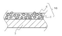
- FIG. 3 is an enlarged cross-sectional view in the vicinity of the bonding layer.
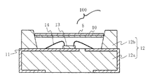
- FIG. 4 is a schematic cross-sectional view of a light emitting device according to an embodiment.
- FIG. 5 is a schematic cross-sectional view of a light emitting device according to another embodiment.
- Embodiment 1 which concerns on this invention concerns on the manufacturing method of a light conversion member.
- the light conversion member 100 manufactured by the manufacturing method is formed by forming the bonding layer 6 containing the phosphor particles 4 on the substrate 5, and is used for a light emitting device, for example.
- the substrate 5 is a substrate having translucency, for example, and is made of, for example, a sapphire substrate.
- the manufacturing method of the optical conversion member concerning Embodiment 1 concerning the present invention is explained in order of a process. (Phosphor particle preparation process) As shown in FIG. 1, phosphor particles 4 are prepared.
- the phosphor particles 4 may be any material that emits light by light from a light emitting element 13 (see FIG.
- white light can be obtained as the whole light emitting device by using YAG phosphor particles, TAG phosphor particles, strontium silicate phosphor particles, and the like that emit yellow light. .
- the phosphor particles 4 are arranged on the bottom surface of the housing 1.
- the phosphor particles 4 having a relatively large particle size can be selectively bonded to the binding layer, whereby phosphor particles having a more uniform particle size can be contained in the binding layer.
- the particle size of the phosphor particles 4 is constant to some extent so that phosphor particles having a more uniform particle size can be contained in the bonding layer.
- the average particle diameter of the phosphor particles 4 is 0.5 to 50 ⁇ m, preferably 1 to 30 ⁇ m, more preferably 10 to 25 ⁇ m. Thereby, the phosphor particles 4 can be easily convected in the housing 1. Moreover, it can be set as the fluorescent substance particle with high luminous efficiency and light extraction efficiency when it finally becomes a light conversion member.
- static electricity may be generated in the phosphor particles themselves, and the adjacent phosphor particles may be closely adhered and aggregated.
- the static electricity generated in the phosphor particles may be removed with an existing static eliminator.
- the phosphor particles 4 can be individually separated, and the phosphor particles can be convected with good reproducibility.
- a kind of phosphor particles are prepared, but a mixture of two or more kinds of phosphor particles may be prepared.
- the bonding layer 6 is prepared.
- the bonding layer 6 is formed on the substrate 5.
- the bonding layer 6 is made of a resin, and can incorporate the phosphor powder 4 into the phosphor particle bonding process (can contain the phosphor powder 4) and can be cured during the bonding layer curing process. Any material can be used, and the material is not limited.
- a thermosetting resin such as a silicone resin or an epoxy resin can be used.
- potting, spraying, spin coating, or the like can be used as a method of forming the bonding layer 6, potting, spraying, spin coating, or the like can be used.
- the viscosity of the resin at the time of application is preferably set to 5000 cp or less, more preferably 1000 cp or less, and more preferably 100 cp or less in order to easily incorporate the phosphor powder 4 into the resin.
- the minimum of the viscosity of resin should just be a viscosity larger than water, for example.
- the substrate 5 only needs to be able to form the bonding layer 6 on its upper surface, and the material is not limited.
- the substrate 5 for example, glass or sapphire can be used.
- the film thickness of the bonding layer 6 before containing the phosphor particles can be 3 ⁇ m or more and less than 100 ⁇ m, preferably 5 ⁇ m or more and less than 70 ⁇ m, more preferably 10 ⁇ m or more and less than 50 ⁇ m.
- the substrate 5 is disposed on the support base 3. As shown in FIG.1 and FIG.2, it is preferable that the support base 3 is provided with the through-hole penetrated to an up-down direction. Since the phosphor powder 4 sent above the bonding layer 6 in the phosphor powder bonding step described later is sent again downward through the through hole, the phosphor particles 4 can be used effectively. It is.
- the phosphor particles 4 are bonded to the bonding layer 6 by convection over the bonding layer 6 (the phosphor particles 4 have wettability with the bonding layer 6 and the weight of the phosphor particles 4 itself. Is taken (filled) into the inside of the bonding layer 6.
- “to make the phosphor particles convection” means that the phosphor particles 4 are caused to flow in opposite directions (up and down directions in FIG. 1) by the wind.
- the method for convection of the phosphor particles 4 is not limited.
- the phosphor particles 4 can be convected above the bonding layer 6 by blowing up the phosphor particles 4 from below the bonding layer 6. This will be described in detail below.
- the blower unit 2 is provided in the housing 1 at a position below the support 3 and away from the side surface of the housing 1.
- the air blowing unit 2 can send wind downward (in the direction of the bottom surface of the housing 1), and can form a wind flow as shown in FIG. That is, wind is sent downward from the blower 2 (step 1), and the wind is directed outward due to the presence of the bottom surface of the housing 1 (step 2), and is sent upward along the side surface of the housing 1 (step 1). 3) Due to the presence of the upper surface of the housing 1, it faces inward (step 4) and is sent again downward. Then, by repeating steps 1 to 4, the wind from the blower unit 2 circulates in the housing 1.
- the phosphor particles 4 are arranged on the bottom surface of the housing 1, the phosphor particles 4 also circulate in the housing 1 by riding on the wind from the blower unit 2.
- FIG. 2 a cross section of the housing is shown in a plan view. Actually, however, the wind sent from the blower 2 entrains the phosphor particles 4 on the bottom surface of the housing 1 and faces the side surface radially. It rises along the entire surface and is collected and circulated again by the upper surface of the housing 1 at the center of the housing.
- the side surface of the casing 1 is preferably cylindrical, and the center of the wind blown out by the blower 2 is the casing 1.
- blower 2 it is preferable to install the blower 2 in the housing 1 so as to coincide with the central axis of the cylindrical side surface.
- the blower 2 is preferably driven to such an extent that the phosphor particles 4 that have fallen from above are not damaged even if they pass through the blower 2.
- the phosphor particles 4 having a certain size have a smaller particle size (small particle size). Rather, it circulates in the housing 1 preferentially and is coupled to the coupling layer 6. The reason for this is not clear, but even if the phosphor particles having a small particle diameter are once sent on the wind, they are likely to stay in the corners of the casing 1 because they are small and lightweight, This is considered to be because it is difficult to reach the bonding layer 6. Furthermore, in general, the smaller the particle size of the phosphor particles, the larger the adhesive force (cohesive force) tends to increase. Therefore, it is difficult for the phosphor particles of small particle size to be sent upward in the wind.
- the phosphor particles used for the light conversion member those having a large particle size are preferable to those having a small particle size.
- those having a large particle size are preferable to those having a small particle size.
- phosphor particles having a small particle size and a large particle size are deposited with a predetermined thickness.
- the phosphor particles having a small particle size have more phosphor particles in the thickness direction than the phosphor particles having a large particle size, light on the surface (interface) of the phosphor particle is present. There is a problem that reflection increases and the light extraction efficiency in the thickness direction decreases.
- phosphor particles with a large particle size have fewer phosphor particles in the thickness direction than phosphor particles with a small particle size, and therefore less light is reflected on the surface of the phosphor particles.
- the light extraction efficiency in the thickness direction is improved.
- the crystal of the surface of the phosphor particles is distorted, it is considered that the phosphor particles cannot emit light efficiently. Therefore, if the phosphor particle has a small particle size, the surface area per certain weight is increased, so that the light emission efficiency is lowered.
- the phosphor particles have a large particle size the surface area per fixed weight is small (since the volume ratio inside the surface in which crystal distortion is suppressed is large), it is possible to emit light efficiently. For these reasons, it is important to suppress the mixing of phosphor particles having a small particle diameter and to form a light conversion member using a phosphor particle having a larger particle diameter preferentially.
- the amount of phosphor particles finally contained in the bonding layer 6 can be controlled by the film thickness of the bonding layer 6. That is, the maximum amount of phosphor particles that can be contained in the bonding layer 6 (the maximum amount of phosphor that can be fixed to the substrate by the bonding layer 6) is smaller as the film thickness of the bonding layer 6 is smaller. The greater the film thickness, the greater. The phosphor particles deposited on the bonding layer 6 exceeding the maximum amount of the phosphor particles in the film thickness can be easily removed because they are not bound by the bonding layer 6. That is, if the bonding layer 6 is thin, the amount of phosphor particles 4 taken into the bonding layer 6 is inevitably reduced. If the bonding layer 6 is thick, the inside of the bonding layer 6 is reduced.
- the amount of the phosphor particles 4 taken in is inevitably increased and the phosphor particles deposited on the bonding layer 6 exceeding the maximum amount of the phosphor particles in the film thickness can be easily removed.
- the amount of the phosphor particles 4 taken into the bonding layer 6 can be easily controlled.
- the phosphor particles 4 are excessively supplied to the bonding layer 6 to such an extent that excess phosphor particles 4 that are no longer filled in the bonding layer 6 are deposited on the bonding layer 6.
- the phosphor particles 4 are supplied in an amount larger than the amount that can be originally contained in the bonding layer 6 having a predetermined thickness under a certain condition.
- the bonding layer 4 formed to have a relatively uniform thickness is filled with the phosphor particles 4 as much as possible throughout the entire region, so that the film thickness direction and the planar direction are compared with the conventional method.
- the distribution of the phosphor particles 4 can be made more uniform.
- color unevenness can be further suppressed when used in a light emitting device.
- the phosphor particles 4 can be simply bonded to the bonding layer 6 without convection of the phosphor particles.
- the phosphor particles 4 can be contained in the bonding layer 6 by simply spreading the phosphor particles from above the bonding layer 6.
- the phosphor particles 4 having a small particle diameter cannot be positively excluded, but it is needless to say that the effect of suppressing color unevenness can be obtained similarly.
- the bonding layer 6 is cured.
- a binder resin and phosphor particles are mixed and then applied to another member such as a light emitting element and cured. Since the phosphor particle bond is bonded to 6 and then cured without being mixed, the light conversion member can be formed by a simpler process.
- the method of curing is not limited, but when the bonding layer 6 is a thermosetting resin, the bonding layer 6 is integrally heated together with the phosphor particles 4 contained therein by heating the bonding layer 6, A light conversion layer 10 composed of the substrate 5, the bonding layer 6 and the phosphor particles 4 is used.
- Excess phosphor particles that have not been taken into the bonding layer 6 and have accumulated on the bonding layer 6 can be removed, for example, by washing away after the bonding layer curing step.
- FIG. 3 shows an enlarged schematic view of the vicinity of the bonding layer obtained by this step.
- the cured bonding layer 6 containing phosphor particles is referred to as a light conversion layer 10.
- the phosphor particles 4 are partially exposed from the surface of the coupling layer 6. This is presumably because the phosphor particles 4 deposited earlier were already taken into the bonding layer 6, and the phosphor particles 4 deposited later were not completely taken into the bonding layer 6.
- the coupling layer 6 is configured to be the uppermost layer.
- a light-transmitting layer that does not include phosphor particles may be formed on the coupling layer 6. Good.
- a light conversion member having a relatively large area for example, a wafer
- the distribution of the phosphor particles tends to be biased as the area becomes larger in the conventional method, but the distribution of the phosphor particles is biased even in the case of the large area in the method according to the present embodiment. Can be suppressed relatively easily. This is because the distribution of the phosphor particles can be controlled only by making the thickness of the coupling layer 6 uniform.
- the recovery efficiency of the phosphor particles 4 is higher than that of the conventional method. This is because the phosphor particles 4 that have not been taken into the bonding layer 6 can be reused, and thus the phosphor particles 4 that are wasted in principle are not generated.
- the light emitting device is configured using the light conversion member and the light emitting element obtained in the first embodiment. As shown in FIG. 4, the light conversion member 100 obtained in the first embodiment and the light emitting element 13 are combined to emit light that can mix the light from the light emitting element 13 and the light from the light converting member. It can be set as a device (light emitting device formation step).
- the light emitting device has a package 12 including a base 12a and a side wall 12b, a pair of lead frames 11 provided along the outer periphery of the package 12, and a bottom surface of a recess formed by the side wall 12b.
- a light emitting element 13 provided on one of the exposed lead frames, a wire 14 that electrically connects each electrode (not shown) of the light emitting element 13 and the corresponding lead frame, and a recess formed by the side wall 12b.
- a light conversion member 100 including a substrate 5 and a coupling layer 6 (including phosphor particles 4) provided above.
- the substrate 5 is on the outside and the coupling layer 6 is on the inside so that the substrate 5 is on the observation surface side.
- the light conversion member 100 can be coupled to the package sidewall 12b via an adhesive made of silicone resin or the like.
- the light emitting element 13 can be a known, for example, blue light emission and green light emission can be GaN-based semiconductor (In X Al Y Ga 1- X-Y N, 0 ⁇ X, 0 ⁇ Y, X + Y ⁇ 1 ).
- the substrate 5 is included as it is as the light conversion member 100, but the substrate 5 may be thinned or removed as necessary.
- the substrate 5 may be thinned or removed as necessary.
- the bonding layer 6 is formed on the substrate 5 by spin coating, the substrate 5 needs to have a certain thickness in the bonding layer forming step.
- the thickness of the substrate 5 may interfere with the work, and in such a case, it is preferable to make the substrate 5 thinner or removed.
- the light emitting device of Embodiment 3 according to the present invention is characterized in that the light conversion layer is formed integrally with the light emitting element by directly forming the coupling layer 6 on the light emitting element 13.
- the method of incorporating the phosphor particles 4 in the bonding layer 6 is the same as in the first embodiment. That is, the bonding layer 6 is directly formed on the light emitting element 13 instead of the substrate 5 (bonding layer forming step), and the phosphor particles 4 are bonded to the bonding layer 6 to form a light emitting device.
- a pair of electrodes 13 c and 13 d are provided on one main surface side of a light emitting element 13 having a pair of opposing main surfaces, the side opposite to one main surface of the light emitting element 13.
- a light conversion layer composed of a bonding layer 6 containing phosphor particles can be provided on the other main surface of the first layer.
- the light emitting device shown in FIG. 5 can be mounted on a conductive member such as a lead frame with one main surface side facing down (face-down mounting), for example.
- the light emitting element 13 is configured to include the growth substrate 13a, the semiconductor portion 13b, the n electrode 13c, and the p electrode 13d, it goes without saying that the structure of the light emitting element 13 is not limited to this.
- the structure of the light emitting element 13 is not limited to this.
- a light conversion layer can also be provided in this area.
- the light emitting element is preferably in the form of a wafer from the viewpoint of work efficiency. In such a case, it is possible to obtain individual light emitting elements by dividing the wafer after the bonding layer curing step.
- a light conversion member having a plurality of bonding layers can be formed by performing the following process after the bonding layer curing process (not shown).
- second phosphor particles different from the phosphor particles 4 are prepared (second phosphor particle preparation step).
- a second bonding layer is formed on the upper surface of the cured bonding layer 6 (first bonding layer) of Embodiment 1 (second bonding layer forming step).
- the second phosphor particles are bound to the second binding layer by causing convection of the second phosphor particles above the second binding layer (second phosphor particle binding step).
- the second bonding layer is cured (second bonding layer curing step).
- the first bonding layer containing the first phosphor particles and the second phosphor particles It can be set as the light conversion member by which the containing 2nd coupling layer was laminated
- the first phosphor particles can be contained up to the upper surface of the first bonding layer, the first phosphor particles and the second phosphor particles are included in the first bonding layer and the second bonding layer. It can be provided substantially continuously. Thereby, since there is substantially no gap between the first phosphor particles and the second phosphor particles, the light extraction efficiency can be improved.
- a bonding layer (first bonding layer) containing phosphor particles (first phosphor particles) that emit long wavelength light in order from the light emitting element side, a short wavelength
- a bonding layer (second bonding layer) containing phosphor particles (second phosphor particles) that emit light of the above.
- the light conversion member is formed in the same manner except that the bonding layer is formed in a desired region of the substrate. By selectively forming the bonding layer on the substrate, the light conversion member can be easily patterned.
- a light emitting device is formed in the same manner except that a bonding layer is selectively formed on the surface of the light emitting element. Thereby, a light conversion layer can be selectively formed on the surface of the light emitting surface of the light emitting element.
- the light conversion member or the light emitting device manufacturing method according to the present invention is applied to various light sources such as an illumination light source, various indicator light sources, an in-vehicle light source, a display light source, a liquid crystal backlight light source, a sensor light source, and a traffic light. Can be used.
Landscapes
- Chemical & Material Sciences (AREA)
- Engineering & Computer Science (AREA)
- Materials Engineering (AREA)
- Organic Chemistry (AREA)
- Life Sciences & Earth Sciences (AREA)
- Chemical Kinetics & Catalysis (AREA)
- General Chemical & Material Sciences (AREA)
- Geochemistry & Mineralogy (AREA)
- Dispersion Chemistry (AREA)
- Composite Materials (AREA)
- Inorganic Chemistry (AREA)
- Led Device Packages (AREA)
Abstract
Description
また、本発明は、色ムラの少ない発光装置を製造することができる発光装置の製造方法を提供することを目的とする。
また、本発明に係る発光装置の製造方法によれば、色ムラの少ない発光装置を製造することができる。
本発明に係る実施形態1は光変換部材の製造方法に係るものである。当該製造方法により作製される光変換部材100は、基板5の上に蛍光体粒子4を含有させた結合層6が形成されてなり、例えば、発光装置に用いられる。基板5は、例えば、透光性を有する基板であり、例えば、サファイア基板からなる。
以下、本発明に係る実施形態1に係る光変換部材の製造方法について工程順に説明する。
(蛍光体粒子準備工程)
図1に示すように、蛍光体粒子4を準備する。蛍光体粒子4は後に準備される発光素子13(図4参照)からの光により発光するものであればよく、その材料は限定されない。例えば、発光素子が青色発光する場合は、黄色に発光するYAG系蛍光体粒子、TAG系蛍光体粒子、ストロンチウムシリケート系蛍光体粒子等とすることで、発光装置全体として白色光を得ることができる。
次に、結合層6を準備する。ここでは、基板5上に結合層6を形成している。
結合層6は樹脂よりなり、蛍光体粒子結合工程の際に蛍光体粉体4を内部に取り込むことができ(蛍光体粉体4を含有することができ)且つ結合層硬化工程の際に硬化できるものであればよく、その材料は限定されない。結合層6の材料としては、例えば、シリコーン樹脂、エポキシ樹脂等の熱硬化性樹脂を使用することができる。結合層6の形成方法としては、ポッティング、スプレー、スピンコート等を利用することができる。塗布する際の樹脂の粘度は、蛍光体粉体4を容易に樹脂内部に取り込むために、好ましくは、5000cp以下、より好ましくは1000cp以下、より好ましくは100cp以下に設定する。また、樹脂の粘度の下限は、例えば、水より大きい粘度であればよい。
次に、蛍光体粒子4を結合層6の上方で対流させることにより、蛍光体粒子4を結合層6に結合させる(蛍光体粒子4は、結合層6との濡れ性やそれ自体の重さにより結合層6の内部に取り込まれる(充填される)。)。本明細書において、「蛍光体粒子を・・・対流させる」とは、蛍光体粒子4を風により相反する方向(図1における上下方向)に流動させることをいう。
本蛍光体粒子結合工程においては、結合層6に充填されなくなった余分な蛍光体粒子4が結合層6に堆積する程度に、蛍光体粒子4を結合層6に過剰に供給することになる。換言すると、本実施形態では、一定条件の下所定の膜厚の結合層6が本来含有できる量以上の蛍光体粒子4を供給している。その結果、比較的均一の厚さに形成された結合層4はその全域で可能な限り蛍光体粒子4が充填された状態となるので、従来の手法と比較して、膜厚方向及び平面方向において蛍光体粒子4の分布がより均一にできる。その結果、発光装置に用いられた際、色ムラをより抑制することができる。
次に、結合層6を硬化させる。例えば、従来の樹脂を用いる方法であれば、バインダーとなる樹脂と蛍光体粒子を混合してから、それを発光素子等の他の部材に塗布等して硬化するが、本実施形態では結合層6に蛍光体粒子結合を結合させてから両者を混合せずにそのまま硬化するので、よりシンプルな工程で光変換部材を形成することができる。硬化の手法は限定されないが、結合層6が熱硬化性樹脂の場合は、結合層6を過熱することにより、結合層6をその内部に含有された蛍光体粒子4と共に一体的に硬化させ、基板5、結合層6及び蛍光体粒子4からなる光変換層10とする。
本発明に係る実施形態2の発光装置は、実施の形態1で得られた光変換部材と発光素子とを用いて構成したものである。
図4に示すように、実施形態1で得られた光変換部材100と発光素子13とを組み合わせて、発光素子13からの光と、光変換部材からの光と、を混色させることができる発光装置とすることができる(発光装置形成工程)。
本発明に係る実施形態3の発光装置は、結合層6を発光素子13に直接形成することにより光変換層を発光素子と一体で構成したことを特徴としている。結合層6に蛍光体粒子4を含有させる方法は実施形態1と同様である。つまり、基板5ではなく発光素子13に結合層6を直接形成し(結合層形成工程)、結合層6に蛍光体粒子4を結合させて発光装置としている。
実施の形態1から3において結合層硬化工程の後に、さらに次の工程を実施することにより、複数層の結合層を有する光変換部材を形成することができる(図示せず)。
実施の形態1の結合層形成工程において、基板の所望の領域に結合層を形成する以外は同様にして、光変換部材を形成する。基板上に結合層を選択的に形成することにより、光変換部材を容易にパターニングすることができる。
実施の形態3の結合層形成工程において、発光素子の表面に選択的に結合層を形成する以外は同様にして発光装置を形成する。これにより、発光素子の発光面の表面に選択的に光変換層を形成することができる。
2・・・送風部
3・・・支持台
4・・・蛍光体粒子
5・・・基板
6・・・結合層
10・・・光変換層
11・・・リードフレーム
12・・・パッケージ
13・・・発光素子
14・・・ワイヤー
100・・・光変換部材
Claims (8)
- 蛍光体粒子を準備する工程と、
基体に樹脂よりなる結合層を形成する工程と、
前記蛍光体粒子を前記結合層に含有させる工程と、
前記結合層を硬化させる工程と、を有することを特徴とする光変換層の形成方法。 - 前記蛍光体粒子を前記結合層に含有させる工程において、前記結合層が含有し得る最大量の蛍光体粒子を含有させる請求項1記載の光変換層の形成方法。
- 前記蛍光体粒子を前記結合層に含有させる工程の後に、該結合層に含有されることなく前記結合層上に付着した過剰の蛍光体粒子を除去する工程を含む請求項2記載の光変換層の形成方法。
- 前記蛍光体粒子を前記結合層に含有させる工程において、前記準備された蛍光体粒子を対流させることにより前記蛍光体粒子を前記結合層に含有させる請求項1~3のうちのいずれか1つに記載の光変換層の形成方法。
- 前記基体は基板であり、
請求項1~4のうちのいずれか1つに記載の光変換層の形成方法により、前記基板の一方の主面に光変換層を形成することを含み、
前記基板と前記光変換層とを含む光変換部材を製造する光変換部材の製造方法。 - 前記光変換層を形成した後に、前記基板を除去することを含み、
前記光変換層を含んでなる光変換部材を製造する請求項5記載の光変換部材の製造方法。 - 請求項5又は6に記載の光変換部材の製造方法により、光変換部材を作製することと、
発光素子を準備することと、
前記発光素子と前記光変換部材とを組み合わせて発光装置とすることとを含むことを特徴とする発光装置の製造方法。 - 前記基体は発光素子であり、
請求項1~4のうちのいずれか1つに記載の光変換層の形成方法により、前記発光素子の発光面に光変換層を形成することを含み、
前記基板と前記光変換層とを含むことを特徴とする発光装置の製造方法。
Priority Applications (2)
| Application Number | Priority Date | Filing Date | Title |
|---|---|---|---|
| JP2012525421A JP5825259B2 (ja) | 2010-07-22 | 2011-07-21 | 光変換層の形成方法、光変換部材の製造方法及び発光装置の製造方法 |
| US13/810,942 US8889443B2 (en) | 2010-07-22 | 2011-07-21 | Method of forming light converting layer, method of manufacturing light converting member, and method of manufacturing light emitting device |
Applications Claiming Priority (4)
| Application Number | Priority Date | Filing Date | Title |
|---|---|---|---|
| JP2010164410 | 2010-07-22 | ||
| JP2010-164410 | 2010-07-22 | ||
| JP2011101301 | 2011-04-28 | ||
| JP2011-101301 | 2011-04-28 |
Publications (1)
| Publication Number | Publication Date |
|---|---|
| WO2012011522A1 true WO2012011522A1 (ja) | 2012-01-26 |
Family
ID=45496940
Family Applications (1)
| Application Number | Title | Priority Date | Filing Date |
|---|---|---|---|
| PCT/JP2011/066544 Ceased WO2012011522A1 (ja) | 2010-07-22 | 2011-07-21 | 光変換層の形成方法、光変換部材の製造方法及び発光装置の製造方法 |
Country Status (4)
| Country | Link |
|---|---|
| US (1) | US8889443B2 (ja) |
| JP (1) | JP5825259B2 (ja) |
| TW (1) | TWI537133B (ja) |
| WO (1) | WO2012011522A1 (ja) |
Families Citing this family (2)
| Publication number | Priority date | Publication date | Assignee | Title |
|---|---|---|---|---|
| US8754435B1 (en) | 2013-02-19 | 2014-06-17 | Cooledge Lighting Inc. | Engineered-phosphor LED package and related methods |
| US8933478B2 (en) | 2013-02-19 | 2015-01-13 | Cooledge Lighting Inc. | Engineered-phosphor LED packages and related methods |
Citations (6)
| Publication number | Priority date | Publication date | Assignee | Title |
|---|---|---|---|---|
| JPS50216Y1 (ja) * | 1970-11-09 | 1975-01-07 | ||
| JPS5029277A (ja) * | 1973-07-20 | 1975-03-25 | ||
| JPH05144375A (ja) * | 1991-11-21 | 1993-06-11 | Dainippon Printing Co Ltd | 蛍光面形成方法 |
| JPH05504600A (ja) * | 1989-08-01 | 1993-07-15 | ジーティーイー プロダクツ コーポレイション | 小さい固形分を被覆する方法及び装置 |
| JP2009183886A (ja) * | 2008-02-07 | 2009-08-20 | Seishin Enterprise Co Ltd | 気流式ふるい分け方法および装置 |
| JP2010006850A (ja) * | 2008-06-24 | 2010-01-14 | Kyocera Corp | 波長変換器および発光装置ならびに照明装置 |
Family Cites Families (9)
| Publication number | Priority date | Publication date | Assignee | Title |
|---|---|---|---|---|
| GB1468175A (en) | 1973-04-19 | 1977-03-23 | Shell Int Research | Inlet system including a fuel vaporizing device for internal combustion engines |
| US5601468A (en) | 1991-10-14 | 1997-02-11 | Dai Nippon Printing Co., Ltd. | Plasma display panel and method for forming fluorescent screens of the same |
| JP2007242624A (ja) | 2000-12-27 | 2007-09-20 | Mitsubishi Chemicals Corp | 発光構造体、発光方法及び照明体 |
| JP4158012B2 (ja) | 2002-03-06 | 2008-10-01 | 日本電気硝子株式会社 | 発光色変換部材 |
| JP3910517B2 (ja) | 2002-10-07 | 2007-04-25 | シャープ株式会社 | Ledデバイス |
| US7679097B2 (en) | 2004-10-21 | 2010-03-16 | Nichia Corporation | Semiconductor light emitting device and method for manufacturing the same |
| JP4615981B2 (ja) * | 2004-12-08 | 2011-01-19 | スタンレー電気株式会社 | 発光ダイオード及びその製造方法 |
| JP4315162B2 (ja) * | 2006-03-10 | 2009-08-19 | パナソニック電工株式会社 | 発光装置の製造方法 |
| JP2009141051A (ja) * | 2007-12-05 | 2009-06-25 | Stanley Electric Co Ltd | シリコーン樹脂を用いた発光ダイオード装置 |
-
2011
- 2011-07-21 US US13/810,942 patent/US8889443B2/en active Active
- 2011-07-21 WO PCT/JP2011/066544 patent/WO2012011522A1/ja not_active Ceased
- 2011-07-21 JP JP2012525421A patent/JP5825259B2/ja not_active Expired - Fee Related
- 2011-07-22 TW TW100126064A patent/TWI537133B/zh active
Patent Citations (6)
| Publication number | Priority date | Publication date | Assignee | Title |
|---|---|---|---|---|
| JPS50216Y1 (ja) * | 1970-11-09 | 1975-01-07 | ||
| JPS5029277A (ja) * | 1973-07-20 | 1975-03-25 | ||
| JPH05504600A (ja) * | 1989-08-01 | 1993-07-15 | ジーティーイー プロダクツ コーポレイション | 小さい固形分を被覆する方法及び装置 |
| JPH05144375A (ja) * | 1991-11-21 | 1993-06-11 | Dainippon Printing Co Ltd | 蛍光面形成方法 |
| JP2009183886A (ja) * | 2008-02-07 | 2009-08-20 | Seishin Enterprise Co Ltd | 気流式ふるい分け方法および装置 |
| JP2010006850A (ja) * | 2008-06-24 | 2010-01-14 | Kyocera Corp | 波長変換器および発光装置ならびに照明装置 |
Also Published As
| Publication number | Publication date |
|---|---|
| JPWO2012011522A1 (ja) | 2013-09-09 |
| TWI537133B (zh) | 2016-06-11 |
| US8889443B2 (en) | 2014-11-18 |
| US20130122620A1 (en) | 2013-05-16 |
| JP5825259B2 (ja) | 2015-12-02 |
| TW201213122A (en) | 2012-04-01 |
Similar Documents
| Publication | Publication Date | Title |
|---|---|---|
| EP3012878B1 (en) | Method for manufacturing a light emitting device | |
| CN104465941B (zh) | 发光器件及其制造方法 | |
| CN110429168B (zh) | 具有磷光体膜的封装发光二极管以及相关的系统和方法 | |
| CN110140218A (zh) | 发光二极管单元 | |
| TWI289942B (en) | Semiconductor light emitting device | |
| JP2010532929A (ja) | 発光素子パッケージ | |
| JP2013175531A (ja) | 発光装置 | |
| JPWO2012029695A1 (ja) | 発光装置とその製造方法 | |
| JP2003234511A (ja) | 半導体発光素子およびその製造方法 | |
| US20120194067A1 (en) | Led device | |
| US9472730B2 (en) | Light emitting device | |
| JP6524624B2 (ja) | 発光装置 | |
| JP2015211058A (ja) | 半導体発光装置およびその製造方法 | |
| JP5825259B2 (ja) | 光変換層の形成方法、光変換部材の製造方法及び発光装置の製造方法 | |
| US11764342B2 (en) | Light emitting device and method for manufacturing light emitting device | |
| TW201351710A (zh) | Led封裝件及其製法 | |
| JP6447557B2 (ja) | 発光装置の製造方法 | |
| JP2014029894A (ja) | 発光装置の製造方法 | |
| KR101865272B1 (ko) | 발광소자 모듈 및 이의 제조방법 | |
| JP2015111626A (ja) | 発光装置およびその製造方法 | |
| KR20110087973A (ko) | 엘이디 패키지, 그 제조방법 및 엘이디 패키지를 구비하는 조명장치 | |
| JP6036103B2 (ja) | 発光装置及びその製造方法 | |
| JP2026006537A (ja) | 発光装置及びその製造方法 | |
| JP2010141354A (ja) | 発光装置およびその製造方法 | |
| CN111987206A (zh) | 量子点led封装器件及制造方法 |
Legal Events
| Date | Code | Title | Description |
|---|---|---|---|
| 121 | Ep: the epo has been informed by wipo that ep was designated in this application |
Ref document number: 11809692 Country of ref document: EP Kind code of ref document: A1 |
|
| WWE | Wipo information: entry into national phase |
Ref document number: 13810942 Country of ref document: US |
|
| WWE | Wipo information: entry into national phase |
Ref document number: 2012525421 Country of ref document: JP |
|
| NENP | Non-entry into the national phase |
Ref country code: DE |
|
| 122 | Ep: pct application non-entry in european phase |
Ref document number: 11809692 Country of ref document: EP Kind code of ref document: A1 |